CN108538331B - First read strategy in memory - Google Patents
First read strategy in memory Download PDFInfo
- Publication number
- CN108538331B CN108538331B CN201810204689.8A CN201810204689A CN108538331B CN 108538331 B CN108538331 B CN 108538331B CN 201810204689 A CN201810204689 A CN 201810204689A CN 108538331 B CN108538331 B CN 108538331B
- Authority
- CN
- China
- Prior art keywords
- voltage
- memory cells
- memory
- read
- channel
- Prior art date
- Legal status (The legal status is an assumption and is not a legal conclusion. Google has not performed a legal analysis and makes no representation as to the accuracy of the status listed.)
- Active
Links
- 230000015654 memory Effects 0.000 title claims abstract description 403
- 238000000034 method Methods 0.000 claims abstract description 56
- 238000010168 coupling process Methods 0.000 claims abstract description 47
- 238000005859 coupling reaction Methods 0.000 claims abstract description 46
- 230000008878 coupling Effects 0.000 claims abstract description 31
- 230000004044 response Effects 0.000 claims abstract description 14
- 239000000758 substrate Substances 0.000 claims description 48
- 238000012360 testing method Methods 0.000 claims description 6
- 238000007667 floating Methods 0.000 abstract description 13
- 230000008569 process Effects 0.000 description 43
- 238000013459 approach Methods 0.000 description 29
- 230000007704 transition Effects 0.000 description 16
- 230000007423 decrease Effects 0.000 description 13
- 239000004065 semiconductor Substances 0.000 description 13
- 239000003990 capacitor Substances 0.000 description 12
- 230000006870 function Effects 0.000 description 12
- 229910052751 metal Inorganic materials 0.000 description 12
- 239000002184 metal Substances 0.000 description 12
- 238000010586 diagram Methods 0.000 description 9
- 238000009826 distribution Methods 0.000 description 8
- 239000000463 material Substances 0.000 description 8
- 238000003491 array Methods 0.000 description 6
- 230000000737 periodic effect Effects 0.000 description 6
- 230000005641 tunneling Effects 0.000 description 6
- 238000013479 data entry Methods 0.000 description 5
- 238000001514 detection method Methods 0.000 description 5
- 238000009792 diffusion process Methods 0.000 description 5
- 230000000694 effects Effects 0.000 description 5
- 230000000903 blocking effect Effects 0.000 description 4
- 239000000872 buffer Substances 0.000 description 4
- 230000005684 electric field Effects 0.000 description 4
- 238000011156 evaluation Methods 0.000 description 4
- 101100481704 Arabidopsis thaliana TMK3 gene Proteins 0.000 description 3
- XUIMIQQOPSSXEZ-UHFFFAOYSA-N Silicon Chemical compound [Si] XUIMIQQOPSSXEZ-UHFFFAOYSA-N 0.000 description 3
- 230000008859 change Effects 0.000 description 3
- 238000004891 communication Methods 0.000 description 3
- 238000005516 engineering process Methods 0.000 description 3
- 238000012545 processing Methods 0.000 description 3
- 229910052710 silicon Inorganic materials 0.000 description 3
- 239000010703 silicon Substances 0.000 description 3
- 239000007787 solid Substances 0.000 description 3
- 238000012795 verification Methods 0.000 description 3
- 101100481702 Arabidopsis thaliana TMK1 gene Proteins 0.000 description 2
- 229910052581 Si3N4 Inorganic materials 0.000 description 2
- 230000004888 barrier function Effects 0.000 description 2
- 230000015572 biosynthetic process Effects 0.000 description 2
- 238000012937 correction Methods 0.000 description 2
- 238000010893 electron trap Methods 0.000 description 2
- 238000002347 injection Methods 0.000 description 2
- 239000007924 injection Substances 0.000 description 2
- 238000012986 modification Methods 0.000 description 2
- 230000004048 modification Effects 0.000 description 2
- 230000002093 peripheral effect Effects 0.000 description 2
- 229910021420 polycrystalline silicon Inorganic materials 0.000 description 2
- 229920005591 polysilicon Polymers 0.000 description 2
- 238000011084 recovery Methods 0.000 description 2
- 230000000630 rising effect Effects 0.000 description 2
- 230000003068 static effect Effects 0.000 description 2
- 239000010409 thin film Substances 0.000 description 2
- 238000012546 transfer Methods 0.000 description 2
- 101100481703 Arabidopsis thaliana TMK2 gene Proteins 0.000 description 1
- 238000000231 atomic layer deposition Methods 0.000 description 1
- 230000008901 benefit Effects 0.000 description 1
- 230000001413 cellular effect Effects 0.000 description 1
- 239000011370 conductive nanoparticle Substances 0.000 description 1
- 230000001808 coupling effect Effects 0.000 description 1
- 230000001419 dependent effect Effects 0.000 description 1
- 238000013461 design Methods 0.000 description 1
- 239000003989 dielectric material Substances 0.000 description 1
- 230000005611 electricity Effects 0.000 description 1
- 230000007613 environmental effect Effects 0.000 description 1
- 239000000835 fiber Substances 0.000 description 1
- 230000036541 health Effects 0.000 description 1
- 230000001788 irregular Effects 0.000 description 1
- 238000012423 maintenance Methods 0.000 description 1
- 230000007246 mechanism Effects 0.000 description 1
- 238000006386 neutralization reaction Methods 0.000 description 1
- 230000003472 neutralizing effect Effects 0.000 description 1
- 150000004767 nitrides Chemical class 0.000 description 1
- 239000000615 nonconductor Substances 0.000 description 1
- 239000012782 phase change material Substances 0.000 description 1
- 230000005529 poole-frenkel effect Effects 0.000 description 1
- 230000008439 repair process Effects 0.000 description 1
- 230000008672 reprogramming Effects 0.000 description 1
- HQVNEWCFYHHQES-UHFFFAOYSA-N silicon nitride Chemical compound N12[Si]34N5[Si]62N3[Si]51N64 HQVNEWCFYHHQES-UHFFFAOYSA-N 0.000 description 1
- 239000011232 storage material Substances 0.000 description 1
- 238000013519 translation Methods 0.000 description 1
- WFKWXMTUELFFGS-UHFFFAOYSA-N tungsten Chemical compound [W] WFKWXMTUELFFGS-UHFFFAOYSA-N 0.000 description 1
- 229910052721 tungsten Inorganic materials 0.000 description 1
- 239000010937 tungsten Substances 0.000 description 1
- 238000010200 validation analysis Methods 0.000 description 1
Images


Classifications
-
- G—PHYSICS
- G11—INFORMATION STORAGE
- G11C—STATIC STORES
- G11C16/00—Erasable programmable read-only memories
- G11C16/02—Erasable programmable read-only memories electrically programmable
- G11C16/06—Auxiliary circuits, e.g. for writing into memory
- G11C16/10—Programming or data input circuits
- G11C16/14—Circuits for erasing electrically, e.g. erase voltage switching circuits
-
- G—PHYSICS
- G11—INFORMATION STORAGE
- G11C—STATIC STORES
- G11C16/00—Erasable programmable read-only memories
- G11C16/02—Erasable programmable read-only memories electrically programmable
- G11C16/06—Auxiliary circuits, e.g. for writing into memory
- G11C16/26—Sensing or reading circuits; Data output circuits
-
- G—PHYSICS
- G11—INFORMATION STORAGE
- G11C—STATIC STORES
- G11C16/00—Erasable programmable read-only memories
- G11C16/02—Erasable programmable read-only memories electrically programmable
- G11C16/06—Auxiliary circuits, e.g. for writing into memory
- G11C16/34—Determination of programming status, e.g. threshold voltage, overprogramming or underprogramming, retention
- G11C16/3404—Convergence or correction of memory cell threshold voltages; Repair or recovery of overerased or overprogrammed cells
- G11C16/3413—Circuits or methods to recover overprogrammed nonvolatile memory cells detected during program verification, usually by means of a "soft" erasing step
Landscapes
- Read Only Memory (AREA)
Abstract
Description
本申请是2018年2月13日所提出的申请号为201810149225.1、发明名称为“存储器中的第一读取对策”的发明专利申请的分案申请。This application is a divisional application of the invention patent application with the application number 201810149225.1 and the invention title "First Read Countermeasure in Memory" filed on February 13, 2018.
技术领域technical field
本技术涉及存储器装置的操作。The present technology relates to the operation of memory devices.
背景技术Background technique
半导体存储器装置在各种电子装置中的使用已经变得越来越流行。例如,非易失性半导体存储器用于蜂巢电话、数码相机、个人数字助理、移动计算装置、非移动计算装置以及其他装置中。The use of semiconductor memory devices in various electronic devices has become increasingly popular. For example, non-volatile semiconductor memory is used in cellular telephones, digital cameras, personal digital assistants, mobile computing devices, non-mobile computing devices, and other devices.
电荷存储材料(诸如浮置栅极)或电荷捕获材料可以用于这样的存储器装置中,以存储表示数据状态的电荷。电荷捕获材料可以垂直地布置在三维(3D)堆叠存储器结构中,或水平地布置在二维(2D)存储器结构中。3D存储器结构的一个示例是位成本可规模化(BiCS)架构,其包括交替的导电和电介质层的堆叠体。Charge storage materials (such as floating gates) or charge trapping materials can be used in such memory devices to store charges representing data states. The charge trapping material can be arranged vertically in a three-dimensional (3D) stacked memory structure, or horizontally in a two-dimensional (2D) memory structure. One example of a 3D memory structure is the Bit Cost Scalable (BiCS) architecture, which includes stacks of alternating conductive and dielectric layers.
存储器装置包含存储器单元,存储器单元可以布置为串,例如,其中在串的端部处提供选择栅极晶体管,以选择性地将串的沟道连接到源极线或位线。然而,操作这样的存储器装置存在各种挑战。A memory device includes memory cells, which may be arranged in strings, eg, with select gate transistors provided at ends of the strings to selectively connect the channels of the strings to source lines or bit lines. However, various challenges exist in operating such memory devices.
发明内容SUMMARY OF THE INVENTION
在一种实施方式中,一种设备包括:存储器单元的区块,所述存储器单元连接到字线集;电压检测器,其连接到字线集中的一个或多个字线,所述电压检测器配置为执行一个或多个字线的电压的评估;以及控制电路,所述控制电路与所述电压检测器通信,所述控制电路配置为基于所述评估来确定用于读取区块中的所选存储器单元的读取电压集。In one embodiment, an apparatus includes: a block of memory cells connected to a set of word lines; a voltage detector connected to one or more word lines in the set of word lines, the voltage detection a control circuit configured to perform an evaluation of the voltage of one or more word lines; and a control circuit in communication with the voltage detector, the control circuit configured to determine, based on the evaluation, a device for use in a read block The read voltage set for the selected memory cell.
一种方法包含:响应于涉及区块的所选存储器单元的读取命令,在读取所选存储器单元之前,确定是否满足将预读取电压脉冲施加到所选存储器单元的条件;如果满足所述条件,在读取所选存储器单元之前,将预读取电压脉冲施加到所选存储器单元;并且如果不满足所述条件,在不将预读取电压脉冲施加到所选存储器单元的情况下读取所选存储器单元。A method includes: in response to a read command involving a selected memory cell of a block, prior to reading the selected memory cell, determining whether a condition for applying a pre-read voltage pulse to the selected memory cell is met; if all the conditions are met; the conditions described, a pre-read voltage pulse is applied to the selected memory cell prior to reading the selected memory cell; and if the condition is not met, the pre-read voltage pulse is not applied to the selected memory cell Read the selected memory cell.
另一相关设备包含用于执行上面的步骤中的每一个的构件。上述构件可以例如包含图1A和图2的存储器装置100的部件。电力控制模块116,例如,控制在存储器操作期间施加到字线、选择栅极线和位线的电力和电压。此外,上述构件可以包含图24A和图24B的部件,包含电压驱动器、开关和通过晶体管。构件还可以包含图1A和图2中的控制电路中的任一个,诸如控制电路110和控制器122。Another related apparatus contains means for performing each of the above steps. The above-described components may, for example, include components of the
在另一实施方式中,设备包括:计时构件,用于周期性地确定刷新存储器单元集的阈值电压的时间,所述存储器单元集包括存储器单元的一个或多个区块;以及用于响应于计时构件而将电压脉冲施加到连接到所述一个或多个区块中的每个区块的存储器单元的字线集的构件。In another embodiment, an apparatus includes: timing means for periodically determining when to refresh a threshold voltage of a set of memory cells, the set of memory cells including one or more banks of memory cells; and for responding to means for timing the means to apply a voltage pulse to a set of word lines connected to memory cells of each of the one or more blocks.
在另一实施方式中,设备包括:存储器单元的区块;以及控制电路,其配置为响应于涉及区块的所选存储器单元的读取或编程命令,感测所选存储器单元,之后执行存储器单元的区块的软擦除。In another embodiment, an apparatus includes: a block of memory cells; and a control circuit configured to, in response to a read or program command involving a selected memory cell of the block, sense the selected memory cell and then execute the memory Soft erase of a block of cells.
附图说明Description of drawings
图1A是示例性存储器装置的框图。1A is a block diagram of an exemplary memory device.
图1B绘示了示例性存储器单元200。FIG. 1B illustrates an
图1C绘示了本文中所公开的各种特征。Figure 1C depicts various features disclosed herein.
图1D绘示了图1A的温度感测电路115的示例。FIG. 1D illustrates an example of the
图2是示例性存储器装置100的框图,绘示了控制器122的附加细节。FIG. 2 is a block diagram of an
图3是包括图1的存储器结构126的示例性3D配置中的区块集的存储器装置600的立体图。FIG. 3 is a perspective view of a
图4绘示了图3的区块中的一个的一部分的示例性截面图。FIG. 4 depicts an exemplary cross-sectional view of a portion of one of the blocks of FIG. 3 .
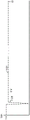
图5绘示了图4的堆叠体中的存储器孔/柱直径的曲线图。FIG. 5 is a graph showing memory hole/pillar diameters in the stack of FIG. 4 .
图6绘示了图4的堆叠体的区域622的特写图。FIG. 6 shows a close-up view of
图7A绘示了根据图4的3D配置中的子区块中的NAND串的示例性视图。FIG. 7A depicts an exemplary view of NAND strings in sub-blocks in the 3D configuration according to FIG. 4 .
图7B绘示了根据图4的示例性区块集中的字线和SGD层。FIG. 7B illustrates word lines and SGD layers in an exemplary block set according to FIG. 4 .
图8A绘示了在与第二读取条件比较的第一读取条件下的存储器单元的示例性Vth分布,其中使用八个数据状态。8A depicts an exemplary Vth distribution for a memory cell under a first read condition compared to a second read condition, where eight data states are used.
图8B绘示了对于图8A的Vth分布的数据的下部、中间和上部页面的示例性位序列,以及相关联的读取电压。Figure 8B depicts exemplary bit sequences for the lower, middle and upper pages of the data for the Vth distribution of Figure 8A, and associated read voltages.
图9绘示了示例性编程操作的波形。FIG. 9 illustrates waveforms of an exemplary programming operation.
图10A绘示了编程操作中的示例性波形的曲线图,示出了字线电压的向上耦合。10A depicts a graph of exemplary waveforms in a programming operation showing upward coupling of word line voltages.
图10B绘示了对应于图10A的沟道电压(Vch)的曲线图。FIG. 10B shows a graph corresponding to the channel voltage (Vch) of FIG. 10A.
图10C绘示了读取操作中的示例性波形的曲线图,示出了字线电压的向上耦合。10C depicts a graph of exemplary waveforms in a read operation showing upward coupling of word line voltages.
图10D绘示了对应于图10C的沟道电压(Vch)的曲线图。FIG. 10D shows a graph corresponding to the channel voltage (Vch) of FIG. 10C.
图10E绘示了图10C的波形,示出了字线的向上耦合电压的衰减。FIG. 10E depicts the waveform of FIG. 10C showing the decay of the up-coupling voltage of the word line.
图10F绘示了根据图10E的沟道电压的曲线图。Figure 10F shows a graph of the channel voltage according to Figure 10E.
图10G绘示了根据图10E和10F的连接到向上耦合字线的存储器单元的Vth的曲线图。Figure 10G depicts a graph of Vth of a memory cell connected to an upwardly coupled word line according to Figures 10E and 10F.
图11A绘示了当在感测操作中控制栅极电压降低时充当电容器的存储器单元上的控制栅极和沟道电压。Figure 11A depicts the control gate and channel voltages on a memory cell acting as a capacitor when the control gate voltage decreases in a sensing operation.
图11B绘示了存储器单元的一部分,示出了在弱编程期间将电子注入到电荷捕获区域中。Figure 11B depicts a portion of a memory cell showing injection of electrons into the charge trapping region during weak programming.
图12A绘示了恰在感测操作的结束时将字线放电之前的示例性存储器串的配置。12A illustrates the configuration of an example memory string just before the word line is discharged at the end of the sense operation.
图12B绘示了恰在感测操作的结束时将字线放电之后的示例性存储器串的配置。Figure 12B illustrates the configuration of an example memory string just after the word lines are discharged at the end of the sensing operation.
图12C绘示了当字线通过沟道向上耦合时的示例性存储器串的配置。12C illustrates an example memory string configuration when word lines are coupled up through channels.
图12D绘示了当字线已经完成向上耦合时的示例性存储器串的配置。Figure 12D illustrates the configuration of an example memory string when the word lines have been coupled up.
图13A绘示了根据图1C中的框10的示例性过程。Figure 13A illustrates an exemplary process according to
图13B绘示了对于不同数据状态的Vth上的移位对时间的曲线图。Figure 13B shows a graph of shift on Vth versus time for different data states.
图13C绘示了读取电压对检测到的字线电压的趋势的曲线图。FIG. 13C shows a graph of read voltage versus detected word line voltage.
图13D绘示了读取电压对检测到的字线电压的曲线图,其中在图13C的示例性实施方式中使用两个读取电压集。Figure 13D depicts a graph of read voltage versus detected word line voltage, where two sets of read voltages are used in the exemplary embodiment of Figure 13C.
图13E绘示了根据图1C中的框10的另一示例性过程。Figure 13E illustrates another exemplary process in accordance with
图14A绘示了根据图1C中的框11的示例性过程。Figure 14A illustrates an exemplary process according to block 11 in Figure 1C.
图14B绘示了根据图1C中的框11的另一示例性过程。Figure 14B illustrates another exemplary process according to block 11 in Figure 1C.
图15A绘示了类似于图10C的读取操作中的示例性波形的曲线图,其中在读取操作之前施加预读取电压脉冲。FIG. 15A depicts a graph of exemplary waveforms in a read operation similar to that of FIG. 10C in which a pre-read voltage pulse is applied prior to the read operation.
图15B绘示了对应于图15A沟道电压(Vch)的曲线图。FIG. 15B shows a graph corresponding to the channel voltage (Vch) of FIG. 15A.
图15C绘示了根据图14A的过程的步骤1402b的预读取电压脉冲持续时间对自从上次感测操作以来的时间的曲线图。Figure 15C depicts a plot of pre-read voltage pulse duration versus time since the last sensing operation according to step 1402b of the process of Figure 14A.
图15D绘示了根据图14A的过程的步骤1402c的预读取电压脉冲持续时间对检测到的字线电压的曲线图。15D depicts a graph of pre-read voltage pulse duration versus detected word line voltage according to step 1402c of the process of FIG. 14A.
图15E绘示了根据图14A的过程的步骤1402d的预读取电压脉冲持续时间对温度的曲线图。Figure 15E depicts a plot of pre-read voltage pulse duration versus temperature according to step 1402d of the process of Figure 14A.
图15F绘示了根据图14A的过程的错误计数对编程脉冲宽度的曲线图。15F depicts a graph of error count versus program pulse width according to the process of FIG. 14A.
图16A绘示了根据图1C中的框12的示例性过程。Figure 16A illustrates an exemplary process according to block 12 in Figure 1C.
图16B绘示了根据图16A的过程的周期性电压脉冲的曲线图。Figure 16B depicts a graph of periodic voltage pulses according to the process of Figure 16A.
图16C绘示了根据图16B的沟道电压的图示。Figure 16C shows a graph of the channel voltage according to Figure 16B.
图16D绘示了根据图16A的框1602a的脉冲周期对温度的曲线图。Figure 16D depicts a graph of pulse period versus temperature according to block 1602a of Figure 16A.
图17A绘示了根据图1C中的框13的示例性过程。Figure 17A illustrates an exemplary process according to block 13 in Figure 1C.
图17B绘示了在正常擦除操作中施加到基板的示例性擦除电压的曲线图。17B depicts a graph of exemplary erase voltages applied to a substrate in a normal erase operation.
图17C绘示了根据图17B的施加到区块中的字线的校验电压的曲线图。Figure 17C shows a graph of verify voltages applied to word lines in a block according to Figure 17B.
图18A绘示了当在根据图17的步骤1702的软擦除操作中,将空穴从基板引入到沟道中并且沟道开始中和时,图12A的示例性存储器串1200的配置。18A illustrates the configuration of the
图18B绘示了当在根据图17和图18A的步骤1702的软擦除操作中,沟道完全中和时的示例性存储器串的配置。18B illustrates the configuration of an exemplary memory string when the channel is fully neutralized in the soft erase operation according to step 1702 of FIGS. 17 and 18A.
图19A绘示了之后是软擦除的读取操作中的示例性波形的图示。19A shows a diagram of exemplary waveforms in a read operation followed by a soft erase.
图19B绘示了在软擦除期间的沟道电压。FIG. 19B shows the channel voltage during soft erase.
图19C绘示了软擦除期间的SGS晶体管电压。Figure 19C shows the SGS transistor voltage during soft erase.
图19D绘示了软擦除期间的p阱电压。Figure 19D shows the p-well voltage during soft erase.
图20A绘示了恰在感测操作的结束时将字线放电之后的示例性存储器串的配置,其中在根据图17的步骤1702的软擦除操作中使用耦合来将SGD和SGS晶体管电压降低。20A illustrates the configuration of an exemplary memory string just after the word line is discharged at the end of a sense operation, where coupling is used to lower the SGD and SGS transistor voltages in a soft erase operation according to step 1702 of FIG. 17 .
图20B绘示了恰在感测操作的结束时将字线放电之后的示例性存储器串的配置,其中在根据图17的步骤1702的软擦除操作中使用驱动的负电压来将SGD和SGS晶体管电压降低。20B illustrates the configuration of an exemplary memory string just after the word lines are discharged at the end of the sense operation, where SGD and SGS are driven negative voltages in a soft erase operation according to step 1702 of FIG. 17 . Transistor voltage drops.
图20C绘示了在根据图17的步骤1702和根据图20A或20B的软擦除操作中,当使用GIDL将空穴从SGD和SGS晶体管引入到沟道中,并且沟道开始中和时,示例性存储器串的配置。Figure 20C shows an example when GIDL is used to introduce holes into the channel from the SGD and SGS transistors, and the channel begins to neutralize, in
图21A绘示了根据图20A和图20C的之后是软擦除的读取操作中的示例性波形的曲线图,其中通过电压在斜降到0V之前斜降到VpassL。21A depicts a graph of exemplary waveforms in a read operation followed by a soft erase in accordance with FIGS. 20A and 20C, where the pass voltage ramps down to VpassL before ramping down to 0V.
图21B绘示了在软擦除的一个示例期间的沟道电压。FIG. 21B depicts the channel voltage during one example of soft erase.
图21C绘示了在软擦除的一个示例期间的SGS和/或SGD晶体管电压。21C illustrates SGS and/or SGD transistor voltages during one example of soft erase.
图21D绘示了在软擦除的一个示例期间的p阱电压。FIG. 21D depicts p-well voltages during one example of soft erase.
图22A绘示了之后是软擦除的读取操作中的示例性波形的曲线图。22A depicts a graph of exemplary waveforms in a read operation followed by a soft erase.
图22B绘示了在软擦除的一个示例期间的沟道电压。FIG. 22B depicts channel voltage during one example of soft erase.
图22C绘示了的软擦除的一个示例期间的SGS和/或SGD晶体管电压。FIG. 22C illustrates SGS and/or SGD transistor voltages during one example of soft erase.
图22D绘示了在软擦除的一个示例期间的p阱电压。22D depicts p-well voltages during one example of soft erase.
图23绘示了图1A的列控制电路中的感测区块51的示例性区块图。FIG. 23 illustrates an exemplary block diagram of the
图24A绘示了用于将电压提供到存储器单元的区块的示例性电路。Figure 24A illustrates an example circuit for providing voltage to a block of memory cells.
图24B绘示了根据图13A的过程的用于检测字线电压的根据图24B的示例性电路。24B illustrates an exemplary circuit according to FIG. 24B for detecting word line voltages according to the process of FIG. 13A.
图25绘示了存储器装置2500,其中根据图16A的过程对于多个裸芯执行电压脉冲,每次一个裸芯。Figure 25 illustrates a
具体实施方式Detailed ways
提供了用于改善存储器装置中的读取操作的精度的技术。也提供了对应的存储器装置。Techniques are provided for improving the accuracy of read operations in memory devices. Corresponding memory devices are also provided.
在一些存储器装置中,存储器单元彼此连结为诸如区块或子区块中的NAND串。每个NAND串包括NAND串的连接到位线的漏极侧的一个或多个漏极侧SG晶体管(SGD晶体管)与NAND串的连接到源极线的源极侧的一个或多个源极侧SG晶体管(SGS晶体管)之间的若干串联连接的存储器单元。此外,存储器单元可以布置有充当控制栅极的公共控制栅极线(例如,字线)。字线集从区块的源极侧延伸到区块的漏极侧。存储器单元可以以其他类型的串以及其他方式连接。In some memory devices, memory cells are linked to each other as NAND strings, such as in blocks or sub-blocks. Each NAND string includes one or more drain side SG transistors (SGD transistors) of the NAND string connected to the drain side of the bit line and one or more source sides of the NAND string connected to the source side of the source line Several series-connected memory cells between SG transistors (SGS transistors). Additionally, the memory cells may be arranged with a common control gate line (eg, a word line) that acts as a control gate. The set of word lines extends from the source side of the block to the drain side of the block. Memory cells can be connected in other types of strings and in other ways.
存储器单元可以包含能够存储用户数据的数据存储器单元,以及不能够存储用户数据的虚设或非数据存储器单元。虚设字线连接到虚设存储器单元。可以在存储器单元的串的漏极和/或源极端提供一个或多个虚设存储器单元,以提供通道梯度上的逐渐过渡。The memory cells may include data memory cells capable of storing user data, and dummy or non-data memory cells incapable of storing user data. The dummy word lines are connected to the dummy memory cells. One or more dummy memory cells may be provided at the drain and/or source terminals of the string of memory cells to provide gradual transitions in channel gradients.
在编程操作期间,根据字线编程顺序来编程存储器单元。例如,编程可以开始于区块的源极侧处的字线并且行进到区块的漏极侧处的字线。在一种方法中,在编程下一字线之前完全编程每个字线。例如,使用一个或多个编程通过(programming pass)来编程第一字线WL0,直到编程完成。接下来,使用一个或多个编程通过来编程第二字线WL1,直到编程完成,以此类推。编程通过可以包含升高的编程电压集,其在相应的编程回路或编程-校验迭代中被施加到字线,诸如图9中所示。可以在每个编程电压之后执行校验操作,以确定存储器单元是否已经完成编程。当对于存储器单元完成编程时,其可以被锁定而不能进一步编程,同时在后续编程回路中对于其他存储器单元继续进行编程。During a programming operation, the memory cells are programmed according to the word line programming sequence. For example, programming may begin with a word line at the source side of the block and proceed to the word line at the drain side of the block. In one approach, each word line is fully programmed before programming the next word line. For example, the first word line WLO is programmed using one or more programming passes until programming is complete. Next, the second word line WL1 is programmed using one or more programming passes until programming is complete, and so on. A programming pass may involve an elevated set of programming voltages that are applied to word lines in corresponding programming loops or program-verify iterations, such as shown in FIG. 9 . A verify operation can be performed after each programming voltage to determine whether the memory cell has completed programming. When programming is complete for a memory cell, it can be locked from further programming while programming continues for other memory cells in subsequent programming loops.
还可以根据子区块编程顺序来编程存储器单元,在这种情况下,在编程另一子区块中的存储器单元之前编程一个子区块或区块的部分中的存储器单元。Memory cells may also be programmed according to the sub-block programming order, in which case memory cells in one sub-block or portion of a block are programmed before memory cells in another sub-block are programmed.
每个存储器单元可以根据编程命令中的写入数据来与数据状态相关联。基于其数据状态,存储器单元将保持在擦除状态或者被编程为编程的数据状态。例如,在每单元一位存储器装置中,存在两个数据状态,包含擦除状态和编程的状态。在每单元两位存储器装置中,存在四个数据状态,包含擦除状态和三个较高的数据状态,称为A,B和C数据状态。在每单元三位存储器装置中,存在八个数据状态,包含擦除状态和七个较高的数据状态,称为A,B,C,D,E,F和G数据状态(见图8A)。在每单元四位存储器装置中,存在十六个数据状态,包含擦除状态和十五个较高的数据状态。所述数据状态可以称为S0,S1,S2,S3,S4,S5,S6,S7,S8,S9,S10,S11,S12,S13,S14和S15数据状态,其中S0为擦除状态。Each memory cell can be associated with a data state according to the write data in the program command. Based on its data state, the memory cell will remain in the erased state or be programmed to the programmed data state. For example, in a one-bit-per-cell memory device, there are two data states, including an erased state and a programmed state. In a two-bit-per-cell memory device, there are four data states, including the erased state and three higher data states, referred to as the A, B, and C data states. In a three-bit-per-cell memory device, there are eight data states, including the erased state and seven higher data states, referred to as the A, B, C, D, E, F, and G data states (see Figure 8A) . In a four-bit-per-cell memory device, there are sixteen data states, including an erased state and fifteen higher data states. The data states may be referred to as S0, S1, S2, S3, S4, S5, S6, S7, S8, S9, S10, S11, S12, S13, S14 and S15 data states, where S0 is the erased state.
在编程存储器单元之后,可以在读取操作中回读(read back)数据。读取操作可以涉及在感测电路确定连接到字线的单元处于导电或不导电状态的同时,将一系列读取电压施加到字线。如果单元处于不导电状态,存储器单元的Vth超过读取电压。读取电压设定为预期在相邻数据状态的阈值电压电平之间的电平。After programming the memory cells, the data can be read back in a read operation. A read operation may involve applying a series of read voltages to a word line while the sensing circuit determines that cells connected to the word line are in a conducting or non-conducting state. If the cell is in a non-conducting state, the Vth of the memory cell exceeds the read voltage. The read voltage is set to a level expected to be between the threshold voltage levels of adjacent data states.
然而,已经观察到,存储器单元的Vth可能根据读取操作何时发生而变化。例如,根据当读取操作发生时字线的向上耦合状态,Vth可能在存储器单元中变化。“第一读取”条件可以限定为其中字线不向上耦合,并且“第二读取”条件可以限定为其中字线向上耦合。However, it has been observed that the Vth of a memory cell may vary depending on when a read operation occurs. For example, Vth may vary among memory cells depending on the up-coupling state of the word lines when a read operation occurs. The "first read" condition may be defined as where the word lines are not coupled up, and the "second read" condition may be defined as where the word lines are coupled up.
在存储器装置中的上电事件之后,存储器单元可以处于第一读取条件。当存储器装置上电以使用时,可以发生检查坏区块的操作。此操作涉及将0V或其他低电压施加到字线。因此,将字线电压的任何向上耦合放电。After a power-up event in the memory device, the memory cells may be in a first read condition. Checking for bad blocks can occur when a memory device is powered up for use. This operation involves applying 0V or other low voltage to the word line. Therefore, any upward coupling of the word line voltage is discharged.
当字线电压设定为低电平时,字线也可以在区块中放电。当在另一区块中执行操作的同时该区块不活动时,可能发生这种情况。因为字线随时间放电,在上次感测操作之后已经过去了长的时间之后,单元也可以处于第一读取条件。字线的向上耦合使得Vth由于无意编程或擦除而在单元中移位。因为处于第一读取条件时字线不显著地向上耦合,不发生此Vth。The word line can also be discharged in the block when the word line voltage is set low. This can happen when an operation is being performed in another block while that block is inactive. Because the word line discharges over time, the cell may also be in the first read condition after a long time has elapsed since the last sensing operation. The upward coupling of the word lines causes Vth to shift in the cell due to unintentional programming or erasing. This Vth does not occur because the word lines are not significantly coupled up when in the first read condition.
当在上次感测操作之后短时间(例如,几秒或几分钟)发生读取时,单元可以处于第二读取条件。因为字线处于第二读取条件时相对强地向上耦合,存在由于字线电压引起的单元的编程或擦除,以及Vth的对应的移位。特别地,具有向上耦合电压的字线可以导致具有相对低的Vth(低于向上耦合电压)的单元(例如,处于较低编程的数据状态的单元)的弱编程,从而导致对于这些单元的Vth向上移位。此外,可以存在具有相对高Vth(高于向上耦合电压)的单元(例如,处于较高编程的数据状态的单元)的弱擦除,从而导致对于这些单元的Vth向下移位。A cell may be in a second read condition when a read occurs a short time (eg, seconds or minutes) after the last sensing operation. Because the word line is relatively strongly coupled up when in the second read condition, there is programming or erasing of the cell due to the word line voltage, and a corresponding shift in Vth. In particular, word lines with up-coupling voltages can result in weak programming of cells with relatively low Vth (below the up-coupling voltage) (eg, cells in lower programmed data states), resulting in Vth for these cells Shift up. In addition, there may be weak erases of cells with relatively high Vth (above the up-coupling voltage) (eg, cells in higher programmed data states), resulting in a downward shift in Vth for these cells.
随着字线放电,单元随时间(例如,一小时)从第二读取条件逐渐转换到第一读取条件。As the word line discharges, the cell gradually transitions from the second read condition to the first read condition over time (eg, one hour).
字线电压的向上耦合由感测操作的电压造成,感测操作诸如为与编程操作相关发生的校验操作,或在编程操作完成之后发生的读取操作。单元的感测涉及将感测电压(例如,读取/校验电压)施加到所选字线。与此同时,读取通过电压施加到未选择字线,并且然后向下步进。由于电容耦合,此向下步进暂时降低沟道电压。还由于电容耦合,当沟道电压升高回其标称电平时,这使得字线电压的升高或向上耦合。对于处于较低数据状态的单元,随着单元的电荷捕获材料中捕获的电子被释放并回到沟道,Vth逐渐降低。对于处于较高数据状态的单元,随着从沟道移除电子,Vth逐渐升高。见图8A。The upward coupling of word line voltages is caused by the voltage of a sense operation, such as a verify operation that occurs in connection with a program operation, or a read operation that occurs after the program operation is complete. Sensing of a cell involves applying a sense voltage (eg, read/verify voltage) to a selected word line. At the same time, the read pass voltage is applied to the unselected word lines, and then steps down. This step down temporarily reduces the channel voltage due to capacitive coupling. Also due to capacitive coupling, this causes a rise or upward coupling of the word line voltage when the channel voltage rises back to its nominal level. For cells in lower data states, Vth gradually decreases as electrons trapped in the cell's charge-trapping material are released and returned to the channel. For cells in higher data states, Vth gradually increases as electrons are removed from the channel. See Figure 8A.
当发生读取操作时,不知道单元是处于第一读取条件还是第二读取条件,或可能处于这两个条件之间某处。一种方法是追踪自从上电事件或先前感测操作以来的经过时间。然而,此经过时间可能不精确地指示字线是否向上耦合,或向上耦合的程度,这是因为诸如环境因素的其他因素和过程变化可能是相关的。此外,将需要分开追踪每个区块。When a read operation occurs, it is not known whether the cell is in the first read condition or the second read condition, or possibly somewhere in between. One approach is to track the elapsed time since a power-up event or previous sensing operation. However, this elapsed time may not be an accurate indicator of whether the word lines are coupled up, or the degree to which they are coupled up, since other factors such as environmental factors and process variations may be relevant. Additionally, each block will need to be tracked separately.
本文中提供的技术解决上述和其他问题。The techniques presented herein address these and other issues.
图1C绘示了本文中所公开的各种特征。第一特征包含检测字线的向上耦合状态,并且相应地设定读取电压(框10)。第二特征包含恰在读取操作之前施加预读取电压脉冲(框11)。第三特征包含将电压脉冲周期性地施加到区块中的全部字线(框12)。这可以独立于读取命令发生,并且涉及将存储器单元的阈值电压刷新为第二读取条件。第四特征包含恰在读取或编程操作之后执行软擦除(框13)。Figure 1C depicts various features disclosed herein. The first feature includes detecting the up-coupling state of the word line and setting the read voltage accordingly (block 10). The second feature involves applying a pre-read voltage pulse just before the read operation (block 11). A third feature includes periodically applying voltage pulses to all word lines in the block (block 12). This can occur independently of the read command and involves refreshing the threshold voltage of the memory cell to the second read condition. A fourth feature involves performing a soft erase (block 13) just after a read or program operation.
以下描述了各种其他特征和优点。Various other features and advantages are described below.
图1A是示例性存储器装置的框图。诸如非易失性存储系统的存储器装置100可以包含一个或多个存储器裸芯108。存储器裸芯108包含存储器单元的存储器结构126(诸如存储器单元的阵列)、控制电路110、以及读取/写入电路128。存储器结构126经由行解码器124通过字线且经由列解码器132通过位线可寻址。读取/写入电路128包含多个感测区块51,52,……,53(感测电路),并且允许并行地读取或编程存储器单元的页面。典型地,控制器122包含在与一个或多个存储器裸芯108相同的存储器装置100(例如,可移除存储卡)中。控制器可以与存储器裸芯分离。命令和数据可以在主机140和控制器122之间经由数据总线120传输,并且在控制器与一个或多个存储器裸芯108之间经由线118传输。1A is a block diagram of an exemplary memory device. A
存储器结构可以为2D或3D。存储器结构可以包括存储器单元的一个或多个阵列,其包括3D阵列。存储器结构可以包括单片3D存储器结构,其中多个存储器级形成在诸如晶片的单个基板之上(且不在基板中),而没有介于中间的基板。存储器结构可以包括单片地形成为具有设置在硅基板上方的有源区域的存储器单元的阵列的一个或多个物理级的任意类型的非易失性存储器。存储器结构可以在具有与存储器单元的操作相关联的电路的非易失性存储器装置中,无论相关联的电路在基板上方或基板内。The memory structure can be 2D or 3D. The memory structure may include one or more arrays of memory cells, including a 3D array. Memory structures may include monolithic 3D memory structures in which multiple memory levels are formed over (and not in) a single substrate, such as a wafer, without intervening substrates. The memory structure may include any type of non-volatile memory monolithically formed as one or more physical levels of an array of memory cells having an active area disposed over a silicon substrate. The memory structure may be in a non-volatile memory device having circuitry associated with the operation of the memory cells, whether the associated circuitry is over or within the substrate.
控制电路110与读取/写入电路128协作以在存储器结构126上执行存储器操作,并且包含状态机112、芯片上地址解码器114、以及电力控制模块116。状态机112提供存储器操作的芯片级控制。如下面进一步讨论的,状态机可以包含时钟112a,以确定自从上次感测操作以来的经过时间。如下面进一步描述的,可以例如为读取电压集提供存储区域113。总体上,存储区域可以存储操作参数和软件/代码。作为示例,计时器113a可以用来确定何时将电压脉冲周期性地施加到字线,如下面关于图13E和16A所描述的。还可以提供温度传感器115。见图1D。
在一个示例中,状态机是通过软件可编程的。在其他实施例中,状态机不使用软件且完全在硬件中(例如,电路)实现。In one example, the state machine is programmable through software. In other embodiments, the state machine does not use software and is implemented entirely in hardware (eg, circuitry).
芯片上地址解码器114提供由主机或存储器控制器使用的地址到由解码器124和132使用的硬件地址之间的地址接口。电力控制模块116控制在存储器操作期间施加到字线、选择栅极线以及位线的电力和电压。其可以包含用于字线、SGS和SGD晶体管以及源极线的驱动器。见图24。在一种方法中,感测区块可以包含位线驱动器。SGS晶体管是NAND串的源极端处的选择栅极晶体管,并且SGD晶体管是NAND串的漏极端处的选择栅极晶体管。On-
在一些实施方式中,部件中的一些可以组合。在各种设计中,部件中的一个或多个(单独或组合)(除了存储器结构126以外)可以构想为至少一个控制电路,其配置为执行本文中所描述的技术,包含本文中所描述的过程的步骤。例如,控制电路可以包含以下项中的任意一个或其组合:控制电路110、状态机112、解码器114和132、电力控制模块116、感测区块51,52,……,53、读取/写入电路128、控制器122等等。In some embodiments, some of the components may be combined. In various designs, one or more of the components (alone or in combination) (other than memory structure 126 ) may be conceived as at least one control circuit configured to perform the techniques described herein, including the steps of the process. For example, the control circuit may include any one or a combination of the following:
芯片外控制器122(其在一个实施例中为电路)可以包括处理器122c、诸如ROM122a和RAM 122b的存储装置(存储器)、以及错误纠正代码(ECC)引擎245。ECC引擎可以纠正若干读取错误。The off-
还可以提供存储器接口122d。与ROM、RAM以及处理器通信的存储器接口是在控制器与存储器裸芯之间提供电接口的电路。例如,存储器接口可以改变信号的格式或定时、提供缓冲区、与浪涌隔离、锁存I/O等等。处理器可以经由存储器接口122d对控制电路110(或存储器裸芯的任意其他部件)发布命令。A
存储装置包括诸如指令集的代码,并且处理器可操作以执行指令集,以提供本文中所描述的功能。可替代地或附加地,处理器可以从存储器结构的存储装置126a(诸如一个或多个字线中的存储器单元的保留区域)访问代码。The storage device includes code, such as a set of instructions, and the processor is operable to execute the set of instructions to provide the functions described herein. Alternatively or additionally, the processor may access code from a
例如,控制器可以使用代码,以访问存储器结构,诸如用于编程、读取以及擦除操作。代码可以包含引导代码和控制代码(例如,指令集)。引导代码是在引导或启动过程期间初始化控制器并使能控制器以访问存储器结构的软件。控制器可以使用代码,以控制一个或多个存储器结构。一经通电,处理器122c从ROM 122a或存储装置126a取回引导代码以执行,并且引导代码初始化系统部件并将控制代码载入到RAM 122b中。控制代码一经被载入到RAM中,由处理器将其执行。控制代码包含驱动器,以执行基本任务,诸如控制和分配存储器、对指令的处理确定优先级、以及控制输入和输出端口。For example, a controller may use code to access memory structures, such as for program, read, and erase operations. The code may include bootstrap code and control code (eg, instruction sets). Boot code is software that initializes the controller and enables the controller to access memory structures during the boot or boot process. The controller may use the code to control one or more memory structures. Upon power up,
总体上,控制代码可以包含指令以执行本文中所描述的包含下面进一步讨论的流程图的步骤的功能,并且提供包含下面进一步讨论的那些电压波形。控制电路可以配置为执行指令,以执行本文中所描述的功能。In general, the control code may contain instructions to perform the functions described herein, including the steps of the flowcharts discussed further below, and to provide voltage waveforms including those discussed further below. The control circuitry may be configured to execute instructions to perform the functions described herein.
在一个示例中,主机是计算装置(例如,膝上式计算机、桌面式计算机、智能手机、平板、数码相机),其包含一个或多个处理器、一个或多个处理器可读取存储装置(RAM、ROM、闪存存储器、硬盘驱动器、固态存储器),其存储处理器可读取代码(例如,软件),以编程一个或多个处理器来执行本文中所描述的方法。主机还可以包含附加的系统存储器、一个或多个输入/输出接口和/或与一个或多个处理器通信的一个或多个输入/输出装置。In one example, the host is a computing device (eg, laptop computer, desktop computer, smartphone, tablet, digital camera) that includes one or more processors, one or more processor-readable storage devices (RAM, ROM, flash memory, hard drive, solid state memory) that stores processor-readable code (eg, software) to program one or more processors to perform the methods described herein. The host may also contain additional system memory, one or more input/output interfaces, and/or one or more input/output devices in communication with one or more processors.
还可以使用除NAND闪存存储器之外的其他类型的非易失性存储器。Other types of non-volatile memory besides NAND flash memory can also be used.
半导体存储器装置包含诸如动态随机存取存储器(“DRAM”)或静态随机存取存储器(“SRAM”)装置的易失性存储器装置,诸如电阻式随机存取存储器(“ReRAM”)、电力可擦除可编程只读存储器(“EEPROM”)、闪存存储器(其也可以视为EEPROM的子集)、铁电式随机存取存储器(“FRAM”)、以及磁阻式随机存取存储器(“MRAM”)的非易失性存储器装置,以及能够存储信息的其他半导体元件。每个类型的存储器装置可以具有不同的配置。例如,闪存存储器装置可以配置为NAND或NOR配置。Semiconductor memory devices include volatile memory devices such as dynamic random access memory ("DRAM") or static random access memory ("SRAM") devices, such as resistive random access memory ("ReRAM"), electrically erasable In addition to programmable read only memory ("EEPROM"), flash memory (which can also be considered a subset of EEPROM), ferroelectric random access memory ("FRAM"), and magnetoresistive random access memory ("MRAM") ”) non-volatile memory devices, and other semiconductor elements capable of storing information. Each type of memory device may have a different configuration. For example, flash memory devices may be configured in a NAND or NOR configuration.
存储器装置可以由无源和/或有源元件以任意组合形成。作为非限制性示例,无源半导体存储器元件包含ReRAM装置元件,其在一些实施例中包含诸如反熔丝或相变材料的电阻率切换存储元件,并且可选地包含诸如二极管或晶体管的转向元件。也作为非限制性示例,有源半导体存储器元件包含EEPROM和闪存存储器装置元件,其在一些实施例中包含含有诸如浮置栅极、导电纳米颗粒、或电荷存储电介质材料的电荷存储区域的元件。Memory devices may be formed from passive and/or active elements in any combination. By way of non-limiting example, passive semiconductor memory elements include ReRAM device elements, which in some embodiments include resistivity-switching memory elements such as antifuses or phase change materials, and optionally include steering elements such as diodes or transistors . Also by way of non-limiting example, active semiconductor memory elements include EEPROM and flash memory device elements, which in some embodiments include elements containing charge storage regions such as floating gates, conductive nanoparticles, or charge storage dielectric materials.
多个存储器元件可以配置为使得它们串联连接或使得每个元件单独地可访问。作为非限制性示例,NAND配置(NAND存储器)的闪存存储器装置典型地含有串联连接的存储器元件。NAND串是串联连接的晶体管集的示例,其包括存储器单元和SG晶体管。Multiple memory elements can be configured such that they are connected in series or such that each element is individually accessible. As a non-limiting example, a flash memory device in a NAND configuration (NAND memory) typically contains memory elements connected in series. A NAND string is an example of a series-connected set of transistors that includes memory cells and SG transistors.
NAND存储器阵列可以配置为使得阵列由存储器的多个串组成,其中串由共用单个位线且作为组访问的多个存储器元件组成。可替代地,存储器元件可以配置为使得每个元件单独地可访问,例如,NOR存储器阵列。NAND和NOR存储器配置是示例,并且可以以其他方式配置存储器元件。A NAND memory array can be configured such that the array consists of multiple strings of memory, where a string consists of multiple memory elements that share a single bit line and are accessed as groups. Alternatively, the memory elements may be configured such that each element is individually accessible, eg, a NOR memory array. NAND and NOR memory configurations are examples, and memory elements may be configured in other ways.
位于基板内和/或上的半导体存储器元件可以布置为二维或三维,诸如2D存储器结构或3D存储器结构。The semiconductor memory elements located in and/or on the substrate may be arranged in two or three dimensions, such as a 2D memory structure or a 3D memory structure.
在2D存储器结构中,半导体存储器元件布置在单个平面中或布置为单个存储器装置级。典型地,在2D存储器结构中,存储器元件布置在平面(例如,在x-y方向上的平面)中,该平面实质上平行于支承存储器元件的基板的主表面延伸。基板可以为晶片,存储器元件的层可以形成在该晶片之上或其中,或者其可以为载体基板,其在形成之后附接到存储器元件。作为非限制性示例,基板可以包含诸如硅的半导体。In a 2D memory structure, semiconductor memory elements are arranged in a single plane or at the level of a single memory device. Typically, in a 2D memory structure, the memory elements are arranged in a plane (eg, a plane in the x-y direction) that extends substantially parallel to the major surface of the substrate supporting the memory elements. The substrate may be a wafer on or in which the layers of memory elements may be formed, or it may be a carrier substrate, which is attached to the memory elements after formation. As a non-limiting example, the substrate may comprise a semiconductor such as silicon.
存储器元件可以以有序阵列布置在单个存储器装置级中,诸如为多个行和/或列。然而,存储器元件可以布置为不规则或非正交配置。存储器元件可以各自具有两个或更多个电极或接触线,诸如位线和字线。The memory elements may be arranged in a single memory device level in an ordered array, such as multiple rows and/or columns. However, the memory elements may be arranged in an irregular or non-orthogonal configuration. The memory elements may each have two or more electrodes or contact lines, such as bit lines and word lines.
3D存储器阵列布置为使得存储器元件占据多个平面或多个存储器装置级,从而形成三维(即,在x、y以及z方向上,其中z方向实质上垂直于基板的主表面,且x和y方向实质上平行于基板的主表面)上的结构。The 3D memory array is arranged such that the memory elements occupy multiple planes or multiple memory device levels, forming three dimensions (ie, in the x, y, and z directions, where the z direction is substantially perpendicular to the major surface of the substrate, and x and y The orientation is substantially parallel to the structure on the major surface of the substrate).
作为非限制性示例,3D存储器结构可以垂直地布置为多个2D存储器装置级的堆叠体。作为另一非限制性示例,3D存储器阵列可以布置为多个垂直列(例如,实质上垂直于基板的主表面(即,在y方向上)延伸的列),其中每个列具有多个存储器元件。列可以2D配置(例如,在x-y平面中)布置,得到具有在多个垂直地堆叠的存储器平面上的元件的存储器元件的3D布置。三维上的存储器元件的其他配置也可以构成3D存储器阵列。As a non-limiting example, a 3D memory structure may be arranged vertically as a stack of multiple 2D memory device levels. As another non-limiting example, a 3D memory array may be arranged in multiple vertical columns (eg, columns extending substantially perpendicular to the major surface of the substrate (ie, in the y-direction)), where each column has multiple memories element. Columns can be arranged in a 2D configuration (eg, in the x-y plane), resulting in a 3D arrangement of memory elements with elements on multiple vertically stacked memory planes. Other configurations of memory elements in three dimensions can also form 3D memory arrays.
作为非限制性示例,在3D NAND存储器阵列中,存储器元件可以耦合在一起,以形成单个水平(例如,x-y)存储器装置级内的NAND串。可替代地,存储器元件可以耦合在一起,以形成穿越多个水平存储器装置级的垂直NAND串。可以设想其他3D配置,其中一些NAND串含有单个存储器级中的存储器元件,而其他串含有跨越多个存储器级的存储器元件。3D存储器阵列还可以设计为NOR配置和ReRAM配置。As a non-limiting example, in a 3D NAND memory array, memory elements may be coupled together to form NAND strings within a single horizontal (eg, x-y) memory device level. Alternatively, memory elements may be coupled together to form vertical NAND strings that span multiple horizontal memory device levels. Other 3D configurations can be envisaged where some NAND strings contain memory elements in a single memory level, while other strings contain memory elements spanning multiple memory levels. 3D memory arrays can also be designed in NOR configuration and ReRAM configuration.
典型地,在单片3D存储器阵列中,一个或多个存储器装置级形成在单个基板上方。可选地,单片3D存储器阵列还可以具有至少部分地在单个基板内的一个或多个存储器层。作为非限制性示例,基板可以包含诸如硅的半导体。在单片3D阵列中,构成阵列的每个存储器装置级的层典型地形成在阵列的下面的存储器装置级的层上。然而,单片3D存储器阵列的相邻存储器装置级的层可以被共用,或在存储器装置级之间具有介于中间的层。Typically, in a monolithic 3D memory array, one or more memory device levels are formed over a single substrate. Optionally, the monolithic 3D memory array may also have one or more memory layers at least partially within a single substrate. As a non-limiting example, the substrate may comprise a semiconductor such as silicon. In a monolithic 3D array, each memory device level layer that makes up the array is typically formed on the underlying memory device level layer of the array. However, layers of adjacent memory device levels of a monolithic 3D memory array may be shared, or have intervening layers between memory device levels.
2D阵列可以分开地形成,并且然后封装在一起,以形成具有多层存储器的非单片存储器装置。例如,可以通过在分开的基板上形成存储器级并且然后将存储器级上下叠置来构建非单片堆叠存储器。可以在堆叠之前将基板减薄或从将其存储器装置级移除,但由于存储器装置级初始地形成在分开的基板之上,得到的存储器阵列不是单片3D存储器阵列。此外,多个2D存储器阵列或3D存储器阵列(单片或非单片)可以形成在分开的芯片上,并且然后封装在一起,以形成堆叠芯片存储器装置。The 2D arrays can be formed separately and then packaged together to form non-monolithic memory devices with multiple layers of memory. For example, non-monolithic stacked memories can be constructed by forming memory levels on separate substrates and then stacking the memory levels on top of each other. The substrates can be thinned or removed from their memory device levels prior to stacking, but since the memory device levels are initially formed over separate substrates, the resulting memory array is not a monolithic 3D memory array. Furthermore, multiple 2D memory arrays or 3D memory arrays (monolithic or non-monolithic) can be formed on separate chips and then packaged together to form a stacked chip memory device.
存储器元件的操作和与存储器元件的通信通常需要相关联的电路。作为非限制性示例,存储器装置可以具有用于控制和驱动存储器元件的电路,以完成诸如编程和读取的功能。此相关联的电路可以在与存储器元件相同的基板上和/或在分开的基板上。例如,用于存储器读取-写入操作的控制器可以位于分开的控制器芯片上和/或在与存储器元件相同的基板上。Operation of the memory element and communication with the memory element typically require associated circuitry. As a non-limiting example, a memory device may have circuitry for controlling and driving memory elements to perform functions such as programming and reading. This associated circuit may be on the same substrate as the memory element and/or on a separate substrate. For example, the controller for memory read-write operations may be located on a separate controller chip and/or on the same substrate as the memory elements.
本领域技术人员将认识到,本技术不限于所描述的2D和3D示例性结构,而是覆盖如本文中所描述的和如本领域技术人员所理解的本技术的精神和范围的全部相关存储器结构。Those skilled in the art will recognize that the present technology is not limited to the 2D and 3D exemplary structures described, but covers all relevant memory as described herein and as understood by those skilled in the art of the spirit and scope of the present technology structure.
图1B绘示了示例性存储器单元200。存储器单元包括接收字线电压Vwl的控制栅极CG、电压Vd下的漏极、电压Vs下的源极以及电压Vch下的沟道。FIG. 1B illustrates an
图1D绘示了图1A的温度感测电路115的示例。电路包含pMOSFET131a,131b和134,双极晶体管133a和133b,以及电阻器R1,R2和R3。I1,I2和I3指代电流。Voutput是提供到模拟到数字(ADC)转换器129的基于温度的输出电压。Vbg是温度相关的电压。电压电平产生电路135使用Vbg来设定若干电压电平。例如,可以通过电阻分压器电路将参考电压下分为若干电平。FIG. 1D illustrates an example of the
ADC将Voutput与电压电平比较,并且在电压电平之中选择最接近匹配,向处理器输出对应的数字值(VTemp)。这是指示存储器装置的温度的数据。在一种方法中,ROM熔丝123存储数据,所述数据将匹配电压电平与温度关联。然后,处理器使用温度来在存储器装置中设定基于温度的参数。The ADC compares Voutput to the voltage levels and selects the closest match among the voltage levels, outputting the corresponding digital value (VTemp) to the processor. This is data indicative of the temperature of the memory device. In one approach, ROM fuses 123 store data that correlates matching voltage levels to temperature. The processor then uses the temperature to set temperature-based parameters in the memory device.
Vbg是通过将晶体管131b两端的基射极间电压(Vbe)与电阻器R2两端的电压降相加而获得的。双极晶体管133a具有比晶体管133b更大的面积(N倍)。PMOS晶体管131a和131b大小相等,并且布置为电流镜像配置,使得电流I1和I2实质上相等。我们已知Vbg=Vbe+R2×I2且I1=Ve/R1,从而I2=Ve/R1。因此,Vbg=Vbe+R2×kT ln(N)/R1×q,其中T为温度,k为玻尔兹曼常数且q是电荷的单元。晶体管134的源极连接到供给电压Vdd,并且晶体管的漏极与电阻器R3之间的节点为输出电压Voutput。晶体管134的栅极连接到与晶体管131a和131b的栅极相同的端子,并且通过晶体管134的电流镜像通过晶体管131a和131b的电流。Vbg is obtained by adding the base-emitter voltage (Vbe) across
图2是示例性存储器装置100的框图,绘示了控制器122的附加细节。如本文中所使用的,闪存存储器控制器是管理闪存存储器上存储的数据并与诸如计算机或电子装置的主机通信的装置。除本文中所描述的特定功能之外,闪存存储器控制器可以具有各种功能。例如,闪存存储器控制器可以格式化闪存存储器以确保存储器正确操作,映射出坏闪存存储器单元,并且分配备用存储器单元以替换将来失效的单元。备用单元的一些部分可以用于保存固件,以操作闪存存储器控制器和实施其他特征。在操作中,当主机需要从闪存存储器读取数据或将数据写入到闪存存储器中时,其将与闪存存储器控制器通信。如果主机提供数据要被读取/写入到的逻辑地址,闪存存储器控制器可以将从主机接收的逻辑地址转换为闪存存储器中的物理地址。(可替代地,主机可以提供物理地址)。闪存存储器控制器也可以执行各种存储器管理功能,诸如但不限于磨损均衡(将写入分散,以避免被重复地写入的存储器的特定区块的磨损)和垃圾收集(在区块装满之后,仅将数据的有效页面移动到新的区块,因此满的区块可以被擦除且重新使用)。FIG. 2 is a block diagram of an
控制器122与非易失性存储器裸芯108之间的接口可以为任意适当的闪速接口。在一个示例中,存储器装置100可以为基于卡的系统,诸如安全数字(SD)或微型安全数字(micro-SD)卡。在替代实施例中,存储器系统可以为嵌入式存储器系统的部分。例如,闪存存储器可以嵌入在主机中,诸如以安装在个人计算机中的固态磁盘(SSD)驱动器的形式。The interface between
在一些实施例中,存储器装置100包含控制器122与非易失性存储器裸芯108之间的单个通道,本文中所描述的主题不限于具有单个存储器通道。In some embodiments, the
控制器122包含与主机相接的前端模块208,与一个或多个非易失性存储器裸芯108相接的后端模块210,以及执行下面将详细描述的功能的各种其他模块。The
例如,控制器的部件可以采取以下形式:设计为与其他部件一起使用的封装的功能硬件单元(例如,电路)、由处理器(例如,微处理器,或通常执行相关功能中的特定功能的处理电路)可执行的程序代码的部分(例如,软件或固件)、或与更大的系统相接的自容式(self-contained)硬件或软件部件。例如,每个模块可以包含应用专用集成电路(ASIC)、现场可编程门阵列(FPGA)、电路、数字逻辑电路、模拟电路、分立电路的组合、门、或任意其他类型的硬件或其组合。可替代地或附加地,每个模块可以包含存储在处理器可读取装置(例如,存储器)中的软件,以编程处理器使得控制器执行本文中所描述的功能。图2所示的架构是一个示例性实施方式,其可以(或可以不)使用图1A中图示的控制器122的部件(例如,RAM、ROM、处理器、接口)。For example, a component of a controller may take the form of a packaged functional hardware unit (eg, a circuit) designed to be used with other components, by a processor (eg, a microprocessor, or generally performing particular ones of the related functions) processing circuitry) executable program code portions (eg, software or firmware), or self-contained hardware or software components that interface with a larger system. For example, each module may contain an application specific integrated circuit (ASIC), field programmable gate array (FPGA), circuit, digital logic circuit, analog circuit, combination of discrete circuits, gates, or any other type of hardware or combination thereof. Alternatively or additionally, each module may contain software stored in a processor-readable device (eg, memory) to program the processor to cause the controller to perform the functions described herein. The architecture shown in FIG. 2 is an example implementation that may (or may not) use the components (eg, RAM, ROM, processor, interface) of the
控制器122可以包含修复电路(recondition circuitry)212,其用于修复存储器单元或存储器的区块。修复可以包含就其当前位置刷新数据或将数据重新编程到新的字线或区块中,作为执行不稳定(erratic)字线维护的一部分,如下面所描述。
再次参考控制器122的模块,缓冲区管理器/总线控制器214管理随机存取存储器(RAM)216中的缓冲区并且控制控制器122的内部总线仲裁(arbitration)。RAM可以包含DRAM和/或SRAM。DRAM或动态随机存取存储器是其中存储器以电荷的形式进行存储的半导体存储器的类型。DRAM中的每个存储器单元由晶体管和电容器制成。数据存储在电容器中。由于泄露,电容器释放电荷,并且因此DRAM为易失性装置。为在存储器中保留数据,装置必须规律地刷新。相比之下,只要供给电力,SRAM或静态随机存取存储器将把值保留。Referring again to the modules of
只读存储器(ROM)218存储系统引导代码。尽管在图2中图示为位于与控制器分开,在其他实施例中,RAM 216和ROM 218中的一个或两者可以位于控制器中。在其他实施例中,RAM和ROM的部分可以都位于控制器122内和控制器之外。此外,在一些实施方式中,控制器122、RAM 216、以及ROM 218可以位于分开的半导体裸芯上。Read only memory (ROM) 218 stores system boot code. Although illustrated in FIG. 2 as being located separate from the controller, in other embodiments one or both of
前端模块208包含主机接口220和物理层接口(PHY)222,其提供与主机或下一级存储体控制器的电接口。主机接口220的类型的选择可以根据所使用的存储器的类型。主机接口220的示例包含但不限于SATA、SATA高速、SAS、光纤通道、USB、PCIe、以及NVMe。主机接口220典型地促进数据、控制信号、以及定时信号的传输。The front end module 208 includes a
后端模块210包含错误纠正控制器(ECC)引擎224,其将从主机接收的数据字节编码,并且对从非易失性存储器读取的数据字节进行解码和错误纠正。命令定序器226产生命令序列(诸如编程和擦除命令序列),以传输到非易失性存储器裸芯108。RAID(独立裸芯的冗余阵列)模块228管理RAID奇偶校验的产生,并且将失效的数据恢复。RAID奇偶校验可以用作正被写入到存储器装置100中的数据的完整性保护的附加级别。在一些情况下,RAID模块228可以为ECC引擎224的部分。应注意到,可以将RAID奇偶校验添加为一般名称(commonname)指代的额外的裸芯或多个裸芯,但其也可以添加在现有裸芯内,例如作为额外平面,或额外区块,或区块内的额外字线。存储器接口230将命令序列提供到非易失性存储器裸芯108,并且从非易失性存储器裸芯接收状态信息。闪存控制层232控制后端模块210的总体操作。Backend module 210 includes an error correction controller (ECC)
存储器装置100的附加部件包含介质管理层238,其执行非易失性存储器裸芯108的存储器单元的磨损均衡。存储器系统还包含其他分立部件240,诸如外部电接口、外部RAM、电阻器、电容器、或可以与控制器122相接的其他部件。在替代实施例中,物理层接口222、RAID模块228、介质管理层238以及缓冲管理/总线控制器214中的一个或多个为可选的部件,其在控制器122中不是必需的。Additional components of the
闪存转换层(flash translation layer,FTL)或介质管理层(MML)238可以集成为闪存管理的部分,其处理闪存错误并与主机相接。特别地,MML可以为闪存管理中的模块且可以负责NAND管理的内务(internals)。特别地,MML 238可以包含存储器装置固件中的算法,其将来自主机的写入转换为对裸芯108的存储器结构126(例如,闪存存储器)的写入。可能需要MML 238,是因为:1)闪存存储器可能具有有限的耐久度;2)闪存存储器可能仅在多个页面中被写入;和/或3)闪存存储器可能无法被写入,除非其作为区块被擦除。MML 238了解闪存存储器的可能对主机不可见的这些潜在限制。相应地,MML 238试图将来自主机的写入转换为到闪存存储器中的写入。可以使用MML 238来识别和记录不稳定位。不稳定位的此记录可以用于评估区块和/或字线(字线上的存储器单元)的健康。A flash translation layer (FTL) or media management layer (MML) 238 may be integrated as part of the flash management, which handles flash errors and interfaces with the host. In particular, the MML may be a module in flash management and may be responsible for the internals of NAND management. In particular,
控制器122可以与一个或多个存储器裸芯108相接。在一个示例中,控制器和多个存储器裸芯(一同包括存储器装置100)实现固态驱动器(SSD),其可以在主机中模拟、替换硬盘驱动器或取代硬盘驱动器使用,作为网络附加存储(NAS)装置等等。附加地,不需要使SSD作为硬盘驱动器工作。
图3是包括图1A的存储器结构126的示例性3D配置的区块集的存储器装置600的立体图。在基板上是存储器单元(存储元件)的示例性区块BLK0,BLK1,BLK2和BLK3,以及具有由区块使用的电路的外围区域604。例如,电路可以包含电压驱动器605,其可以连接到区块的控制栅极层。在一种方法中,区块中的共同高度处的控制栅极层被共同地驱动。基板601还可以载有区块之下的电路,以及图案化为导电路径的一个或多个下部金属层,以携载电路的信号。区块形成在存储器装置的中间区域602中。在存储器装置的上部区域603中,一个或多个上部金属层图案化为导电路径,以携载电路的信号。每个区块包括存储器单元的堆叠区域,其中堆叠体的交替级代表字线。在一种可能的方法中,每个区块具有相对的分层侧,垂直接触体从相对的分层侧朝上延伸到上部金属层,以形成去往导电路径的连接。尽管绘示了四个区块作为示例,可以使用在x和/或y方向上延伸的两个或更多个区块。3 is a perspective view of a
在一种可能的方法中,区块在平面中,并且平面在x方向上的长度表示到字线的信号路径在一个或多个上部金属层中延伸的方向(字线或SGD线方向),并且平面在y方向上的宽度表示到位线的信号路径在一个或多个上部金属层中延伸的方向(位线方向)。z方向表示存储器装置的高度。区块还可以布置在多个平面中。In one possible approach, the block is in a plane, and the length of the plane in the x-direction represents the direction in which the signal path to the wordline extends in one or more upper metal layers (wordline or SGD line direction), And the width of the plane in the y direction represents the direction in which the signal path of the bit line extends in the one or more upper metal layers (bit line direction). The z-direction represents the height of the memory device. Blocks can also be arranged in multiple planes.
图4绘示了图3的一个区块的一部分的示例性截面图。区块包括交替的导电层与电介质层的堆叠体616。在此示例中,除了数据字线层(或字线)WLL0-WLL10之外,导电层包括两个SGD层、两个SGS层以及四个虚设字线层(或字线)WLD1,WLD2,WLD3和WLD4。电介质层标记为DL0-DL19。此外,绘示了堆叠体包括NAND串NS1和NS2的区域。每个NAND串包含存储器孔618或619,所述存储器孔填充有形成与字线相邻的存储器单元的材料。堆叠体的区域622在图6中以更多细节示出。FIG. 4 depicts an exemplary cross-sectional view of a portion of a block of FIG. 3 . The block includes a
堆叠体包含基板611。在一种方法中,源极线SL的一部分在基板中包括n型源极扩散层611a,其与区块中的存储器单元的每个串的源极端接触。在一种可能的实施方式中,n型源极扩散层611a形成在p型阱区域611b中,p型阱区域611b进而形成在n型阱区域611c中,n型阱区域611c进而形成在p型半导体基板611d中。在一种方法中,n型源极扩散层可以由平面中的全部区块共用。The stack includes a
NS1具有堆叠体的底部616b处的源极端613和堆叠体的顶部616a处的漏极端615。可以跨堆叠体周期性地提供诸如局部互连体617的局部互连体。局部互连体可以为金属填充的狭缝,其延伸穿过堆叠体,诸如以将源极线/基板连接到堆叠体上方的线。可以在字线的形成期间使用狭缝并且随后用金属填充。局部互连体包括绝缘区域617b内的导电区域617a(例如,金属)。还绘示了位线BL0的一部分。导电通孔621将NS1的漏极端615连接到BL0。NS1 has a
在一种方法中,存储器单元的区块包括交替的控制栅极和电介质层的堆叠体,并且存储器单元布置于在堆叠体中垂直地延伸的存储器孔中。In one approach, a block of memory cells includes a stack of alternating control gates and dielectric layers, and the memory cells are arranged in memory holes extending vertically in the stack.
在一种方法中,每个区块包括阶梯边缘,其中垂直互连体连接到每个层(包含SGS、WL以及SGD层),并且朝上延伸到去往电压源的水平路径。In one approach, each block includes a stepped edge with vertical interconnects connected to each layer (including the SGS, WL, and SGD layers) and extending up to the horizontal path to the voltage source.
例如,此示例在每个串中包含两个SGD晶体管、两个漏极侧虚设存储器单元、两个源极侧虚设存储器单元以及两个SGS晶体管。总体上,虚设存储器单元的使用是可选的,并且可以提供一个或多个虚设存储器单元。此外,在存储器串中可以提供一个或多个SGD晶体管和一个或多个SGS晶体管。For example, this example includes two SGD transistors, two drain side dummy memory cells, two source side dummy memory cells, and two SGS transistors in each string. In general, the use of dummy memory cells is optional, and one or more dummy memory cells may be provided. Additionally, one or more SGD transistors and one or more SGS transistors may be provided in the memory string.
可以提供绝缘区域620,以将SGD层的部分彼此分开,从而为每个子区块提供一个独立地驱动的SGD线。在此示例中,字线层对于两个相邻子区块是共用的。还参见图7B。在另一种可能的实施方式中,绝缘区域620向下延伸到基板以将字线层分开。在此情况下,字线层在每个子区块中分开。尽管,在任意情况下,区块的字线层可以在其端部彼此连结,使得它们在区块内被共同地驱动,如图7B所示。Insulating
图5绘示了图4的堆叠体中的存储器孔/柱直径的图示。垂直轴线与图4的堆叠体对准,并且绘示了由存储器孔618和619中的材料形成的柱的宽度(wMH)(例如,直径)。在这样的存储器装置中,穿过堆叠体蚀刻的存储器孔具有很高的深宽比(aspect ratio)。例如,约25-30的深度对直径比是常见的。存储器孔可以具有圆形截面。由于蚀刻工艺,存储器孔和所得的柱宽度可能沿着孔的长度变化。典型地,直径从存储器孔的顶部到底部逐渐变小(实线)。即,存储器孔是渐缩的,在堆叠体的底部处变窄。在一些情况下,轻微变窄发生在靠近选择栅极的孔的顶部处,使得直径从存储器孔的顶部到底部逐渐变小之前稍微变宽(长断划线)。例如,在此示例中,存储器孔宽度在堆叠体中的WL9的级处是最大的。存储器孔宽度在WL10的级处稍小,并且在WL8到WL0的级处逐渐变小。FIG. 5 is an illustration of memory hole/pillar diameters in the stack of FIG. 4 . The vertical axis is aligned with the stack of FIG. 4 and depicts the width (wMH) (eg, diameter) of the posts formed from the material in the
由于存储器孔与所得的柱的直径上的不均匀性,存储器单元的编程和擦除速度可能基于其沿着存储器孔的位置而变化。在存储器孔的底部处的相对较小直径的情况下,跨隧道氧化物的电场相对较强,使得编程和擦除速度对于与存储器孔的相对较小直径部分相邻的字线中的存储器单元更高。字线向上耦合的量和放电因此比与存储器孔的相对较大直径部分相邻的字线中的存储器单元相对较大。Due to the non-uniformity in the diameter of the memory holes and the resulting pillars, the programming and erasing speeds of memory cells may vary based on their location along the memory holes. With a relatively small diameter at the bottom of the memory hole, the electric field across the tunnel oxide is relatively strong, so that programming and erasing speeds are relatively slow for memory cells in word lines adjacent to the relatively small diameter portion of the memory hole higher. The amount of upward coupling and discharge of the word line is thus relatively greater than the memory cells in the word line adjacent to the relatively larger diameter portion of the memory hole.
在另一种可能的实施方式中,由短断划线表示,堆叠体制造为两个层级。底部层级首先形成有相应的存储器孔。然后将顶部层级形成有与底部层级中的存储器孔对准的相应的存储器孔。每个存储器孔是渐缩的,使得形成双渐缩存储器孔,其中从堆叠体的底部到顶部,宽度增加、然后减小并且再次增加。In another possible embodiment, indicated by the short dashed line, the stack is manufactured in two levels. The bottom level is first formed with corresponding memory holes. The top level is then formed with corresponding memory holes that align with the memory holes in the bottom level. Each memory hole is tapered such that a double tapered memory hole is formed where the width increases, then decreases and increases again from the bottom to the top of the stack.
图6绘示了图4的堆叠体的区域622的特写图。存储器单元形成在堆叠体的不同级处,在字线层与存储器孔的交点处。在此示例中,在虚设存储器单元682和683以及数据存储器单元MC上方提供SGD晶体管680和681。可以例如使用原子层沉积来沿着存储器孔630的侧壁(SW)和/或在每个字线层内沉积若干层。例如,由存储器孔内的材料形成的每个柱699或立柱可以包含电荷捕获层663或诸如硅氮化物(Si3N4)或其他氮化物的薄膜、隧穿层664(隧道氧化物)、沟道665(例如,包括多晶硅)、以及电介质芯666。字线层可以包含阻挡氧化物/阻挡高k材料660、金属势垒(barrier)661、以及诸如作为控制栅极的钨的导电金属662。例如,提供控制栅极690,691,692,693和694。在此示例中,除金属之外的全部层提供在存储器孔中。在其他方法中,层中的一些可以在控制栅极层中。附加的柱类似地形成在不同的存储器孔中。柱可以形成NAND串的柱状有源区域(AA)。FIG. 6 shows a close-up view of
当编程存储器单元时,电子存储在电荷捕获层的与存储器单元相关联的部分中。这些电子从沟道被引入到电荷捕获层中,并且穿过隧穿层。存储器单元的Vth正比于存储的电荷的量(例如,随着存储的电荷的量增加)而升高。在擦除操作期间,电子返回到沟道。When programming a memory cell, electrons are stored in the portion of the charge trapping layer associated with the memory cell. These electrons are introduced into the charge trapping layer from the channel and pass through the tunneling layer. The Vth of a memory cell increases proportionally to the amount of stored charge (eg, as the amount of stored charge increases). During the erase operation, electrons return to the channel.
存储器孔中的每一个可以填充有多个环状层,环状层包括阻挡氧化物层、电荷捕获层、隧穿层、以及沟道层。存储器孔中的每一个的芯区域填充有主体材料,并且多个环状层在每个存储器孔中的芯区域与字线之间。Each of the memory holes may be filled with a plurality of annular layers including a blocking oxide layer, a charge trapping layer, a tunneling layer, and a channel layer. The core region of each of the memory holes is filled with a body material, and a plurality of annular layers are between the core region and the word lines in each memory hole.
NAND串可以认为具有浮置主体沟道,因为沟道的长度不形成在基板上。此外,通过堆叠体中上下叠置的多个字线层来提供NAND串,且通过电介质层彼此分开。A NAND string can be considered to have a floating body channel because the length of the channel is not formed on the substrate. Furthermore, the NAND strings are provided by a plurality of word line layers stacked on top of each other in the stack and separated from each other by a dielectric layer.
图7A绘示了根据图4的3D配置的子区块中的NAND串的示例性视图。绘示了示例性存储器单元,其在x方向上沿着每个子区块中的字线延伸。为了简明,每个存储器单元绘示为立方体。SB0包含NAND串700n,701n,702n和703n。SB1包含NAND串710n,711n,712n和713n。SB2包含NAND串720n,721n,722n和723n。SB3包含NAND串730n,731n,732n和733n。位线连接到NAND串集。例如,位线BL0连接到NAND串700n,710n,720n和730n,位线BL1连接到NAND串701n,711n,721n和731n,位线BL2连接到NAND串702n,712n,722n和732n,并且位线BL3连接到NAND串703n,713n,723n和733n。感测电路可以连接到每个位线。例如,感测电路400,400a,400b和400c分别连接到位线BL0,BL1,BL2和BL3。NAND串为从基板朝上延伸的垂直存储器串(例如,垂直串)的示例。FIG. 7A illustrates an exemplary view of NAND strings in a sub-block according to the 3D configuration of FIG. 4 . Exemplary memory cells are depicted extending in the x-direction along word lines in each subblock. For simplicity, each memory cell is shown as a cube. SB0 contains NAND strings 700n, 701n, 702n and 703n. SB1 contains NAND strings 710n, 711n, 712n and 713n. SB2 contains NAND strings 720n, 721n, 722n and 723n. SB3 contains NAND strings 730n, 731n, 732n and 733n. The bit lines are connected to the NAND string sets. For example, bit line BL0 is connected to
对于所选单元,可以每次在一个字线和一个子区块中发生编程和读取。这允许每个所选单元由相应的位线和/或源极线控制。例如,SB0中的存储器单元的示例性集795连接到WLL4。类似地,包括SB1,SB2和SB3中的数据存储器单元的集796,797和798连接到WLL4。For selected cells, programming and reading can occur one wordline and one subblock at a time. This allows each selected cell to be controlled by a corresponding bit line and/or source line. For example, an
图7B绘示了根据图4的示例性区块集中的字线和SGD层。绘示了区块BLK0,BLK1,BLK2和BLK2。绘示了每个区块中的字线层(WLL),且连同示例性SGD线。每个子区块中提供了一个SGD线。BLK0包含子区块SB0,SB1,SB2和SB3。每个圈表示存储器孔或串。实际上,子区块在x方向上延长且含有数千个存储器串。附加地,比所绘示的那些更多的区块在基板上布置为多个行。字线层和SGD/SGS层可以从行解码器2410接收电压。也参见图24A和24B。FIG. 7B illustrates word lines and SGD layers in an exemplary block set according to FIG. 4 . Blocks BLK0, BLK1, BLK2 and BLK2 are depicted. The word line layer (WLL) in each block is depicted, along with exemplary SGD lines. One SGD line is provided in each subblock. BLK0 contains subblocks SB0, SB1, SB2 and SB3. Each circle represents a memory hole or string. In practice, a subblock extends in the x-direction and contains thousands of memory strings. Additionally, more blocks than those depicted are arranged in rows on the substrate. The word line layer and the SGD/SGS layer may receive voltages from the
图8A绘示了存储器单元的处于与第二读取条件相比较的第一读取条件的示例性Vth分布,其中使用八个数据状态。八个数据状态仅为示例,因为也可以使用其他数目,诸如四个、十六个或更多。对于Er,A,B,C,D,E,F和G状态,我们已知分别处于第二读取条件下的Vth分布820,821,822,823,824,825,826和827,且已知分别处于第一读取条件下的820a,821a,822a,823a,824a,825a,826a和827a。对于A,B,C,D,E,F和G状态,我们分别具有编程校验电压VvA,VvB,VvC,VvD,VvE,VvF和VvG。还绘示的分别是第二读取条件下的读取电压VrAH,VrBH,VrCH,VrDH,VrEL,VrFL和VrGL,以及分别是处于第一读取条件下的读取电压VrAL,VrBL,VrCL,VrDL,VrEH,VrFH和VrGH。还绘示的分别是111,110,100,000,010,011,001和101的位的示例性编码。位格式是:UP/MP/LP。在擦除操作期间使用擦除校验电压VvEr。8A depicts an exemplary Vth distribution for a memory cell at a first read condition compared to a second read condition, where eight data states are used. The eight data states are only an example, as other numbers, such as four, sixteen, or more, could also be used. For Er, A, B, C, D, E, F and G states, we know the
此示例指示,当数据状态相对较高或较低时,与第二读取条件相比,第一读取条件的Vth分布上的移位比当数据状态为中间范围时相对较大。对于逐渐变低或变高的数据状态,移位可以逐渐变大。在一个示例中,在第一读取条件下,VrAL,VrBL,VrCL和VrDL的读取电压分别对于A,B,C和D的相对较低状态是最佳的,并且VrEH,VrFH和VrGH的读取电压分别对于E,F和G的相对较高状态是最佳的。类似地,在第二读取条件下,VrAH,VrBH,VrCH和VrDH的读取电压分别对于A,B,C和D的相对较低状态是最佳的,并且VrEL,VrFL和VrGL的读取电压分别对于E,F和G的相对较高状态是最佳的。从而,在一种可能的实施方式中,在对于较低状态的第一读取条件下,每个状态两个读取电压中的较低者是最佳的,并且在对于较高状态的第一读取条件下,每个状态两个读取电压中的较高者是最佳的。This example indicates that when the data state is relatively high or low, the shift on the Vth distribution for the first read condition is relatively larger than when the data state is in the middle range compared to the second read condition. The shift can be progressively larger for progressively lower or higher data states. In one example, under the first read condition, the read voltages of VrAL, VrBL, VrCL, and VrDL are optimal for the relatively low states of A, B, C, and D, respectively, and the VrEH, VrFH, and VrGH The read voltages are optimal for the relatively high states of E, F and G, respectively. Similarly, under the second read condition, the read voltages of VrAH, VrBH, VrCH and VrDH were optimal for the relatively low states of A, B, C and D, respectively, and the reads of VrEL, VrFL and VrGL The voltages are optimal for the relatively high states of E, F and G, respectively. Thus, in one possible implementation, at the first read condition for the lower state, the lower of the two read voltages per state is optimal, and at the first read condition for the higher state Under a read condition, the higher of the two read voltages per state is optimal.
最佳读取电压通常在相邻数据状态的Vth分布之间的中间。相应地,随着Vth分布移位,最佳读取电压移位。The optimum read voltage is usually midway between the Vth distributions of adjacent data states. Accordingly, as the Vth distribution shifts, the optimum read voltage shifts.
当自从上次编程或读取操作存在长延迟时,可以发生第一读取条件。示例性序列为:编程区块,等待一小时,然后读取区块。当存在上电/下电时,也可以发生第一读取条件。示例性序列为:编程区块,上电/下电,然后读取区块。当存在其他区块的编程或读取时,也可以发生第一读取条件。示例性序列是:编程一个区块,编程另一区块,然后读取该一个区块。The first read condition can occur when there is a long delay since the last program or read operation. An exemplary sequence is: program the block, wait an hour, then read the block. The first read condition can also occur when there is a power up/down. An exemplary sequence is: program the block, power up/down, then read the block. The first read condition can also occur when there is programming or reading of other blocks. An exemplary sequence is: program one block, program another block, then read the one block.
图8B绘示了数据的下部、中间和上部页面的示例性位序列,以及相关联的读取电压。在此情况下,存储器单元各自以八个数据状态中的一个存储三位的数据。绘示了对于每个状态的示例性位分配。下部、中间或上部位可以分别表示下部、中间或上部页面的数据。除了擦除状态Er之外,使用七个编程的数据状态A,B,C,D,E,F和G。利用这些位序列,可以通过使用VrA和VrE的读取电压(例如,控制栅极或字线电压)读取存储器单元来确定下部页面的数据。如果Vth<=VrA或Vth>VrE,则下部页面(LP)位=1。如果VrA<Vth<=VrE,则LP=0。总体上,可以在施加读取电压的同时,由感测电路感测存储器单元。如果存储器单元在感测时间处于导电状态,则其阈值电压(Vth)小于读取电压。如果存储器单元处于不导电状态,其Vth大于读取电压。FIG. 8B illustrates exemplary bit sequences for lower, middle, and upper pages of data, and associated read voltages. In this case, the memory cells each store three bits of data in one of eight data states. Exemplary bit assignments for each state are depicted. The lower, middle, or upper bits can represent data for the lower, middle, or upper pages, respectively. In addition to the erased state Er, seven programmed data states A, B, C, D, E, F and G are used. Using these bit sequences, the data of the lower page can be determined by reading the memory cells using the read voltages of VrA and VrE (eg, control gate or word line voltages). Lower Page (LP) bit=1 if Vth<=VrA or Vth>VrE. LP=0 if VrA<Vth<=VrE. In general, the memory cells can be sensed by the sensing circuit while the read voltage is being applied. If the memory cell is in the conductive state at the sensing time, its threshold voltage (Vth) is less than the read voltage. If the memory cell is in a non-conducting state, its Vth is greater than the read voltage.
用于读取数据的页面的读取电压是通过在每个状态的编码的位(码字)中从0到1或1到0的转换来确定的。例如,LP位在Er和A之间从1转换到0,并且在D和E之间从0转换到1。相应地,LP的读取电压为VrA和VrE。The read voltage used to read a page of data is determined by transitions from 0 to 1 or 1 to 0 in the encoded bits (codewords) of each state. For example, the LP bit transitions from 1 to 0 between Er and A, and from 0 to 1 between D and E. Accordingly, the read voltages of LP are VrA and VrE.
可以通过使用读取电压VrB,VrD和VrF读取存储器单元,来确定中间页面的数据。如果Vth<=VrB或VrD<Vth<=VrF,则中间页面(MP)位=1。如果VrB<Vth<=VrD或Vth>VrF,则MP=0。例如,MP位在A和B之间从1转换到0,在C和D之间从0转换到1,并且在E和F之间从1转换到0。相应地,MP的读取电压为VrB,VrD和VrF。The data of the middle page can be determined by reading the memory cells using the read voltages VrB, VrD and VrF. If Vth<=VrB or VrD<Vth<=VrF, the middle page (MP) bit=1. MP=0 if VrB<Vth<=VrD or Vth>VrF. For example, the MP bit transitions from 1 to 0 between A and B, 0 to 1 between C and D, and 1 to 0 between E and F. Accordingly, the read voltages of MP are VrB, VrD and VrF.
可以通过使用VrC和VrG的读取电压读取存储器单元,来确定上部页面的数据。如果Vth<=VrC或Vth>VrG,则上部页面(UP)位=1。如果VrC<Vth<=VrG,则UP=0。例如,UP位在B和C之间从1转换到0,并且在F和G之间从0转换到1。相应地,UP的读取电压为VrC和VrG。读取电压绘示为VrA,VrB,VrC,VrD,VrE,VrF和VrG,其中这些电压中的每一个可以表示第一读取值或第二读取值,取其最佳值。The data of the upper page can be determined by reading the memory cells using the read voltages of VrC and VrG. If Vth<=VrC or Vth>VrG, the upper page (UP) bit=1. UP=0 if VrC<Vth<=VrG. For example, the UP bit transitions from 1 to 0 between B and C, and from 0 to 1 between F and G. Accordingly, the read voltages of UP are VrC and VrG. The read voltages are depicted as VrA, VrB, VrC, VrD, VrE, VrF and VrG, where each of these voltages can represent a first read value or a second read value, whichever is best.
图9绘示了示例性编程操作的波形。水平轴线绘示了编程回路(PL)编号,并且垂直轴线绘示了控制栅极或字线电压。总体上,编程操作可以涉及将脉冲列施加到所选字线,其中脉冲列包含多个编程回路或编程-校验迭代。编程-校验迭代的编程部分包括编程电压,并且编程-校验迭代的校验部分包括一个或多个校验电压。FIG. 9 illustrates waveforms of an exemplary programming operation. The horizontal axis depicts the programming loop (PL) number, and the vertical axis depicts the control gate or word line voltage. In general, a programming operation may involve applying a pulse train to a selected word line, where the pulse train contains multiple programming loops or program-verify iterations. The program portion of the program-verify iteration includes program voltages, and the verify portion of the program-verify iteration includes one or more verify voltages.
在一种方法中,每个编程电压包含两个步进。此外,在此示例中使用了增量步进脉冲编程(Incremental Step Pulse Programming,ISPP),其中编程电压在每个相继的编程回路中使用固定或变化的步进大小向上步进。此示例在完成编程的单个编程通过中使用ISPP。ISPP还可以在多通过操作中的每个编程通过中使用。In one approach, each programming voltage contains two steps. Additionally, Incremental Step Pulse Programming (ISPP) is used in this example, where the programming voltage is stepped up using a fixed or varying step size in each successive programming loop. This example uses ISPP in a single programming pass that completes programming. ISPP can also be used in each programming pass in a multi-pass operation.
波形900包含一系列编程电压901,902,903,904,905,……906,其被施加到为编程所选择的字线并施加到相关联的非易失性存储器单元集。作为示例,基于正被校验的目标数据状态,可以在每个编程电压之后提供一个或多个校验电压。可以在编程与校验电压之间将0V施加到所选字线。例如,在编程电压901和902中的每一个之后,可以分别施加VvA和VvB的A状态和B状态校验电压(波形910)。在编程电压903和904中的每一个之后,可以施加VvA,VvB和VvC的A状态,B状态和C状态校验电压(波形911)。在若干附加编程回路(未示出)之后,可以在最终编程电压906之后施加VvE,VvF和VvG(波形912)的E状态,F状态和G状态校验电压。
图10A绘示了编程操作中的示例性波形的曲线图,示出了字线电压的向上耦合。所示的时间周期表示一个编程-校验迭代。水平轴线绘示了时间,并且垂直轴线绘示了字线电压Vwl。编程电压1000从t0-t4施加到所选字线并且达到Vpgm的幅度。编程电压可以暂时暂停在诸如Vpass的中间电平,以避免可能具有不期望的耦合效应的单个大转换。从t0-t19将通过电压1005施加到未选择字线,并且达到Vpass的幅度,其足够高以提供处于导电状态的单元,从而感测(例如,校验)操作可以对于所选字线的单元发生。通过电压包含升高部分、固定幅度部分(例如,在Vpass)和降低部分。可选地,通过电压可以相对于编程电压更快地升高,从而在t0达到Vpass。10A depicts a graph of exemplary waveforms in a programming operation showing upward coupling of word line voltages. The time period shown represents one program-verify iteration. The horizontal axis plots time, and the vertical axis plots word line voltage Vwl. The
将校验电压1010施加到所选字线。在此示例中,施加了全部七个校验电压,一个接一个。在此示例中使用八级存储器装置。在t8,t9,t10,t11,t12,t13和t14处分别施加VvA,VvB,VvC,VvD,VvE,VvF和VvG的校验电压。在每个校验电压期间可以激活感测电路。从t15-t16,波形从VvG降低到0V或其他稳定状态电平。A verify
对于未选择的字线,Vpass上的降低将使得单元从导电状态转换到不导电状态。特别地,当Vpass降低低于截止电平Vcutoff(t18处的点线),单元的沟道将变为截止,例如,单元将变得不导电。当单元变得不导电时,其充当电容器,其中控制栅极是一个板且沟道是另一个板。当Vcg<Vcutoff或Vcg<(Vth+Vsl)时,单元变得不导电,其中Vcg是单元的控制栅极电压(字线电压),Vth是单元的阈值电压,并且Vsl是源极线电压,源极线电压进而近似是单元的源极端子处的电压。对于处于最高的编程状态(例如,G状态)的单元,Vth可以与VvG一样低(或由于编程后电荷损失而更低),并且与图8A中的Vth分布827或827a中的G状态的上部尾部处的Vth一样高。Vcutoff因此可以与VVG+Vsl一样低或与G状态上部尾部的Vth+Vsl一样高。随着通过电压1005从Vcutoff降低到0V,沟道电容地向下耦合相似的量,如图10B中的曲线1015所示。For unselected word lines, a drop on Vpass will cause the cell to transition from a conducting state to a non-conducting state. In particular, when Vpass falls below the cutoff level Vcutoff (dotted line at t18), the channel of the cell will become cutoff, eg, the cell will become non-conductive. When the cell becomes non-conductive, it acts as a capacitor, where the control gate is one plate and the channel is the other plate. The cell becomes non-conductive when Vcg<Vcutoff or Vcg<(Vth+Vsl), where Vcg is the cell's control gate voltage (word line voltage), Vth is the cell's threshold voltage, and Vsl is the source line voltage, The source line voltage in turn is approximately the voltage at the source terminal of the cell. For cells in the highest programmed state (eg, G-state), Vth can be as low as VvG (or lower due to post-program charge loss), and is comparable to the upper portion of the G-state in
当Vsl较大时,在沟道被截止时电压摆动将较大。然而,由于Vch=Vsl,Vch的最小向下耦合电平将基本上与Vsl无关。例如,Vsl=1V的情况下,字线电压上的6V摆动(例如,Vcutoff=6V)将导致与Vsl=0V的情况下的字线电压上的5V摆动(例如,Vcutoff=5V)大约相同的Vch的最小向下耦合电平。When Vsl is larger, the voltage swing will be larger when the channel is turned off. However, since Vch=Vsl, the minimum down-coupling level of Vch will be substantially independent of Vsl. For example, a 6V swing on the wordline voltage (eg, Vcutoff=6V) with Vsl=1V will result in approximately the same 5V swing on the wordline voltage (eg, Vcutoff=5V) with Vsl=0V Minimum down-coupling level for Vch.
曲线1012表示字线电压从t19-t20的向上耦合。向上耦合绘示为相对快速地发生,但这不是按比例的。实际上,校验操作(例如,从t5-t19)可能消耗约100微秒,而字线的向上耦合可能显著地更久,为毫秒范围,诸如10毫秒。
图10B绘示了对应于图10A的沟道电压(Vch)的曲线图。对于未选择的存储器串(不具有在当前编程回路中被编程的单元的串),Vch将在编程电压期间增压至诸如8V的电平(未示出),例如,从t0-t4。此增压通过提供处于不导电状态下的未选择串的SGD和SGS晶体管以使得Vch浮置而实现。当Vpass和Vpgm施加到字线时,Vch由于电容耦合耦合得更高。对于所选存储器串(具有在当前编程回路中被编程的单元的串),Vch典型地被接地,如在编程电压期间所示。FIG. 10B shows a graph corresponding to the channel voltage (Vch) of FIG. 10A. For unselected memory strings (strings that do not have cells programmed in the current programming loop), Vch will be boosted to a level such as 8V (not shown) during the programming voltage, eg, from t0-t4. This boosting is accomplished by providing the SGD and SGS transistors of the unselected strings in a non-conducting state to float Vch. When Vpass and Vpgm are applied to the word line, Vch is coupled higher due to capacitive coupling. For the selected memory string (string with cells being programmed in the current programming loop), Vch is typically grounded, as shown during the programming voltage.
在校验电压期间,对于所选存储器串,Vch可以例如初始地在约1V。对于所选存储器串的沟道,Vch约与Vsl相同。基于所使用的感测的类型来设定Vsl。示例包含Vsl为约1V的负感测,以及Vsl为约0V且使用负字线电压的正感测。无论Vsl的电平或所使用的感测的类型,都适用本文中所描述的技术。During the verify voltage, Vch may, for example, be initially at about 1V for the selected memory string. For the channel of the selected memory string, Vch is about the same as Vsl. Vsl is set based on the type of sensing used. Examples include negative sense where Vsl is about IV, and positive sense where Vsl is about 0V and uses a negative word line voltage. The techniques described herein apply regardless of the level of Vsl or the type of sensing used.
沟道从t18-t19电容地向下耦合到最低电平,并且然后从t19-t20开始返回到例如0V的最终电平。如果允许字线的电压在t19开始浮置,电压(曲线1012)通过Vch的升高而电容地耦合得更高。字线的电压浮置到峰值电平Vwl_coupled_up,从而达到第二读取条件。例如,Vcutoff可以为6V,使得字线电压上存在6V改变(例如,6-0V),其耦合到沟道。在Vch的初始值为1V和90%耦合比的情况下,最小Vch可以为例如约1-6×0.9=-4.4V。相应地,Vch上存在4.4V升高,其耦合到字线,例如,单元的控制栅极。Vwl_coupled_up可以为约4.4×0.9=4V。通过将字线从字线驱动器断开,将字线的电压浮置。The channel is capacitively coupled down to the lowest level from t18-t19, and then returns to a final level, eg, 0V, starting from t19-t20. If the voltage of the word line is allowed to start to float at t19, the voltage (curve 1012) is capacitively coupled higher by the rise in Vch. The voltage of the word line is floated to the peak level Vwl_coupled_up, thereby reaching the second read condition. For example, Vcutoff may be 6V, such that there is a 6V change (eg, 6-0V) in the word line voltage, which is coupled to the channel. In the case where the initial value of Vch is 1V and the coupling ratio is 90%, the minimum Vch may be, for example, about 1-6×0.9=−4.4V. Accordingly, there is a 4.4V boost on Vch, which is coupled to the word line, eg, the control gate of the cell. Vwl_coupled_up may be about 4.4×0.9=4V. By disconnecting the word line from the word line driver, the voltage of the word line is floated.
图10C绘示了读取操作中的示例性波形的曲线图,示出了字线电压的向上耦合。读取操作类似于校验操作,因为两者都是感测操作且都可以提供字线电压的向上耦合。水平轴线绘示了时间,并且垂直轴线绘示了字线电压Vwl。通过电压1115,1116和1117分别从t0-t3,t4-t8和t9-t12被施加到未选择的字线,并且具有Vpass的幅度。通过电压包含升高部分、Vpass的部分和降低部分。对于下部、中间和上部页面中的每一个,读取电压分别包含分开的波形1120(在VrAH和VrEL的电平处),1121(在VrBH,VrDH和VrFL的电平处)以及1122(在VrCH和VrGL的电平处),与图8A和图8B一致。作为示例,读取电压对于第二读取条件被优化,并且被施加到所选字线。在此示例中使用八级存储器装置。10C depicts a graph of exemplary waveforms in a read operation showing upward coupling of word line voltages. The read operation is similar to the verify operation in that both are sense operations and can provide upward coupling of word line voltages. The horizontal axis plots time, and the vertical axis plots word line voltage Vwl.
对于未选择的字线,Vpass上的降低将使得单元从导电状态转换到不导电状态,如所讨论的。t13处的点线指示G状态单元何时变得不导电。随着通过电压1117从Vcutoff降低到0V,沟道电容地向下耦合相似的量,如由图10D中的曲线1035所表示的。随着沟道电压在t14之后升高,字线电压浮置并耦合得更高到Vwl_coupled_up。For unselected word lines, a drop on Vpass will cause the cell to transition from a conducting state to a non-conducting state, as discussed. The dotted line at t13 indicates when the G-state cell becomes non-conductive. As
图10D绘示了对应于图10C的沟道电压(Vch)的曲线图。沟道从t13-t14电容地向下耦合到Vch_min的最低电平,并且然后从t14-t15开始返回到例如0V的最终电平。如果允许字线的电压在t14开始浮置,则电压(曲线1032)通过Vch(曲线1035)上的升高而电容地耦合得更高。字线的电压浮置到Vwl_coupled_up的峰值电平,如所讨论的。FIG. 10D shows a graph corresponding to the channel voltage (Vch) of FIG. 10C. The channel is capacitively coupled down to the lowest level of Vch_min from t13-t14, and then returns to a final level, eg, 0V, starting from t14-t15. If the voltage of the word line is allowed to float starting at t14, the voltage (curve 1032) is capacitively coupled higher by the rise on Vch (curve 1035). The voltage of the word line is floated to the peak level of Vwl_coupled_up, as discussed.
图10E绘示了图10C的波形,其示出了字线的向上耦合的电压的衰减。时间比例与图10A-10D中不同,并且表示更长的时间周期,诸如一个或多个小时。曲线1123绘示了时间周期t0-t1中的读取电压(对应于图10C中的波形1120-1122)。曲线1123a绘示了通过电压(对应于图10C中的波形1115-1117)。曲线1125绘示了由于耦合(在时间周期t1-t2中)Vwl上升到向上耦合电平(Vwl_coupled_up),以及之后Vwl在时间周期t2-t3中的衰减。总体上,与衰减的时间周期相比,Vwl上的升高发生得相对较快。FIG. 10E depicts the waveform of FIG. 10C showing the decay of the up-coupled voltage of the word line. The time scales are different from those in Figures 10A-10D and represent longer periods of time, such as one or more hours.
图10F绘示了根据图10E的沟道电压的曲线图。在时间周期t1-t2中,降低之后是升高(曲线1126)。Vch从t2-t3为约0V(曲线1127)。Figure 10F shows a graph of the channel voltage according to Figure 10E. In the time period t1-t2, the decrease is followed by the increase (curve 1126). Vch is about 0V from t2-t3 (curve 1127).
图10G绘示了连接到向上耦合字线的存储器单元的Vth的曲线图,与图10E和10F一致。对于诸如A状态的示例性数据状态下的单元,从t0-t1,Vth处于初始电平Vth_initial。这表示第一读取条件。由于与Vch上的升高同时的耦合,Vth从t1-t2(曲线1128)上升到Vth_coupled_up的峰值电平。这表示第二读取条件。Vth然后从t1-t3逐渐降低回到Vth_initial。Figure 10G depicts a graph of the Vth of a memory cell connected to an upwardly coupled word line, consistent with Figures 10E and 10F. For a cell in an exemplary data state such as the A state, from t0-t1, Vth is at the initial level Vth_initial. This represents the first read condition. Vth rises from t1-t2 (curve 1128) to the peak level of Vth_coupled_up due to the simultaneous coupling with the rise on Vch. This represents the second read condition. Vth then gradually decreases back to Vth_initial from t1-t3.
图11A绘示了存储器单元上的控制栅极电压和沟道电压,在感测操作中,当控制栅极电压下降时,存储器单元充当电容器。第一读取问题由3D的字线平面或层的堆叠导致,其中存储器单元的沟道被浮置且不像在2D闪存NAND架构中那样被耦合到基板。氧化物-氮化物-氧化物(ONO)层中的字线耦合和电子捕获是第一读取问题的源头。FIG. 11A depicts the control gate voltage and channel voltage on a memory cell that acts as a capacitor when the control gate voltage drops in a sensing operation. The first read problem is caused by the stacking of word line planes or layers in 3D, where the channels of the memory cells are floating and not coupled to the substrate as in 2D flash NAND architectures. Word line coupling and electron trapping in oxide-nitride-oxide (ONO) layers are the source of the first read problem.
如所讨论的,在读取/校验操作之后,当施加在字线上的读取通过电压(Vpass)斜降时,在Vpass下降到5V时,G状态单元(例如,具有5V的Vth)将沟道截止。当Vpass进一步下降到Vss时,浮置沟道电势则被推低到负值。接下来,在读取操作结束之后,通过吸引正电荷,上面示出的沟道中的负电压(约-4.5V)升高。由于数据字线被浮置,将沟道充电所需的空穴的量相对小,因此所选的和未选择的字线可以快速地向上耦合到大约4V(假定90%的耦合比)。字线上的电势保持在约4V一段时间。这在隧道ONO层中吸引和捕获电子,并且对于较低或较高数据状态分别导致Vth向上移位或向下移位。由于字线耦合到浮置沟道电势,字线电压从而在读取操作之后提升到约4V。As discussed, after a read/verify operation, when the read pass voltage (Vpass) applied to the word line ramps down, when Vpass drops to 5V, the G-state cell (eg, with a Vth of 5V) Turn off the channel. As Vpass drops further to Vss, the floating channel potential is pushed down to a negative value. Next, after the read operation ends, the negative voltage (about -4.5V) in the channel shown above rises by attracting positive charges. Since the data word lines are floating, the amount of holes required to charge the channel is relatively small, so selected and unselected word lines can quickly couple up to about 4V (assuming a 90% coupling ratio). The potential on the word line remains at about 4V for some time. This attracts and traps electrons in the tunnel ONO layer and results in an upward or downward shift in Vth for lower or higher data states, respectively. Since the word line is coupled to the floating channel potential, the word line voltage thus rises to about 4V after the read operation.
顶部板表示控制栅极或字线,并且底部板表示沟道。电容器1040表示当字线电压从8V(Vpass)下降到5V(Vcutoff,诸如VvG或稍微更高)且Vch=0V时的存储器单元。电容器1042表示当字线电压达到0V时的存储器单元,使得Vch向下耦合到约-4.5V。电容器1044表示当相关联的字线电压开始浮置时的存储器单元。电容器1046表示当相关联的字线电压在第二读取条件下达到Vwl_coupled_up时的存储器单元。如果存储器单元的Vth小于4V(例如,单元处于擦除状态或较低编程的状态),则存储器单元将被弱编程,使得其Vth升高。如果存储器单元的Vth大于4V(例如,单元处于较高编程的状态),则存储器单元将被弱擦除,使得其Vth下降。电容器1048表示在已经经过很长时间(例如,一小时或更久)之后的存储器单元,使得字线已经放电到第一读取条件。The top plate represents the control gate or word line, and the bottom plate represents the channel.
当数据字线电压浮置时,为沟道充电所需的空穴的量相对小。因此,作为示例,所选的字线可以相对快速地向上耦合到约4V。所选字线上的电势保持为约4V一端时间,吸引隧道氧化物-氮化物-氧化物(ONO)层中捕获的电子,并且使得Vth向上移位。如果在下一读取操作之前的等待足够久,则字线的向上耦合的电势将放电,并且捕获的电子将被释放。将再次发生第一读取条件。When the data word line voltage is floating, the amount of holes required to charge the channel is relatively small. Thus, as an example, a selected word line may be coupled up to about 4V relatively quickly. The potential on the selected word line is maintained at about 4V for one end time, attracting trapped electrons in the tunnel oxide-nitride-oxide (ONO) layer and shifting Vth upward. If the wait is long enough before the next read operation, the up-coupled potential of the word line will discharge and the trapped electrons will be released. The first read condition will occur again.
图11B绘示了图6的存储器单元MC的一部分,示出了在弱编程期间将电子注入到电荷捕获区域中。存储器单元包含控制栅极694、金属势垒661a、阻挡氧化物660a、电荷捕获层663、隧穿层664、沟道665和电介质芯666。由于提升的字线电压,产生电场(E),其将电子(见示例电子1050)吸引到电荷捕获层中,使Vth升高。此弱编程可以由Poole–Frenkel效应造成,其中电绝缘体可以导通电力。这是一种通过捕获的电子隧穿。弱擦除类似地涉及电场,其将电子从电荷捕获层排斥,使Vth降低。FIG. 11B depicts a portion of the memory cell MC of FIG. 6 showing injection of electrons into the charge trapping region during weak programming. The memory cell includes
图12A绘示了恰在感测操作的结束时将字线放电之前的示例性存储器串1200的配置。例如,这恰在字线电压开始从Vpass斜降之前,例如,在图10A中的t17和图10C中的t12。如提到的,第一读取问题由高Vth单元(例如,G状态单元)在字线的放电期间将沟道截止造成。Vch通过放电字线向下耦合。随后,空穴进入沟道,以中和沟道电压,例如,Vch从负电压升高到约0V。例如,此升高将字线电压向上耦合到约4V。此提升的字线电压最终导致隧道氧化物与多晶硅隧道之间的界面中的电子捕获、以及存储器单元的电荷捕获层中的电荷重新分布,使单元中的一些的Vth升高到第二读取条件。在已经经过一些时间(诸如一个或多个小时)之后,或如果字线暴露于稳定状态电压一段时间,字线将最终放电回到约0V。此放电是由于电流通过SGS晶体管并且泄露到基板中。单元然后返回到第一读取条件。最佳读取电平基于单元是处于第一读取条件还是第二读取条件(或之间的某处)而变化。如果读取电平对于第一读取条件进形优化且存在第二读取条件,或如果读取电平对于第二读取条件进行优化且存在第一读取条件,则将导致大量的读取错误。FIG. 12A illustrates the configuration of an
存储器串1200在p阱1205与位线1202之间延伸,并且包含SGS晶体管控制栅极1210与SGD晶体管控制栅极1216之间的存储器单元控制栅极1211,1212,1213,……,1214和1215。串包含存储器薄膜层1203内的沟道区域1204(例如,电荷捕获层内的隧穿层)。还绘示了中央电介质芯1201。在截面图中示出了串,其中控制栅极和层环绕在存储器孔周围。此外,作为示例,具有控制栅极1211和1215的存储器单元被编程为G状态(在此示例中的最高状态),并且具有控制栅极1212-1214的存储器单元处于任意状态。
SGD控制栅极处于Vsgd的电压(例如,3-4V),存储器单元控制栅极1211-1215处于Vpass的电压(例如,8-10V),SGS控制栅极处于Vsgs的电压(例如,3-4V),p阱可以处于1V(Vsl)并且位线可以处于1-2V。因为为了感测操作而将感测电路激活,示例性电子(“e-”)从位线进入沟道。这导致约0V的沟道电压。在字线的放电或斜降期间,G状态单元截止(变得不导电),使得沟道电压浮置并且向下耦合,如所提到的。The SGD control gates are at a voltage of Vsgd (eg, 3-4V), the memory cell control gates 1211-1215 are at a voltage of Vpass (eg, 8-10V), and the SGS control gates are at a voltage of Vsgs (eg, 3-4V) ), the p-well can be at 1V (Vsl) and the bit line can be at 1-2V. Exemplary electrons ("e-") enter the channel from the bit line as the sensing circuit is activated for the sensing operation. This results in a channel voltage of about 0V. During the discharge or ramp-down of the word line, the G-state cell turns off (becomes non-conductive), allowing the channel voltage to float and couple down, as mentioned.
图12B绘示了恰在感测操作的结束时将字线放电之后的示例性存储器串的配置。在此时,沟道电压为负(Vch<0V),如由减少的电子的数目所表示,并且控制栅极中的每一个达到0V。位线电压也可以设定为0V。Figure 12B illustrates the configuration of an example memory string just after the word lines are discharged at the end of the sensing operation. At this time, the channel voltage is negative (Vch<0V), as represented by the reduced number of electrons, and each of the control gates reaches 0V. The bit line voltage can also be set to 0V.
图12C绘示了当字线通过沟道向上耦合时的示例性存储器串的配置。负沟道电压造成跨SGS晶体管的横向场,其造成空穴从p阱逐渐进入沟道。空穴将跨SGS晶体管的场中和并且与电子结合,逐渐使得沟道电压朝向0V升高。在此时,字线电压浮置,使得它们随着Vch升高而向上耦合。这由标记“浮置得更高”指示。12C illustrates an example memory string configuration when word lines are coupled up through channels. The negative channel voltage causes a lateral field across the SGS transistor, which causes holes to gradually enter the channel from the p-well. The holes will neutralize and combine with the electrons across the field of the SGS transistor, gradually increasing the channel voltage towards 0V. At this point, the word line voltages are floating so that they couple up as Vch rises. This is indicated by the flag "float higher".
图12D绘示了当字线已经完成向上耦合时的示例性存储器串的配置。在此情况下,沟道完全中和,使得Vch=0V。作为示例,字线电压处于约4V的向上耦合的电平。Figure 12D illustrates the configuration of an example memory string when the word lines have been coupled up. In this case, the channel is completely neutralized such that Vch=0V. As an example, the word line voltage is at an up-coupled level of about 4V.
图13A绘示了根据图1C中的框10的示例性过程。此特征包含检测字线的向上耦合状态并且相应地设定读取电压。步骤1300包含接收区块中的所选存储器单元(例如,连接到所选字线)的读取命令。例如,可以从主机在控制器122处接收命令。在其他情况下,在存储器装置100(图1A)内使读取命令内部地产生。步骤1301包含感测区块中的字线电压。在一种方法中,感测到的字线是在区块中预定的,并且不必与连接到所选存储器单元的所选字线相同。对一个或多个字线的感测是可能的。例如,电压检测器可以配置为执行对一个或多个字线的电压的评估。对于进一步的示例性细节,见图24B。步骤1302包含基于感测的字线电平而选择读取电压集。感测的字线电平指示存储器单元处于第一读取条件还是第二读取条件,或之间的某处。参见例如图13B-13D。步骤1303包含在区块中使用所选读取电压集来执行读取操作。在此方法中,可以基于字线的当前向上耦合状态,来选择将读取错误最小化的最佳读取电压集。Figure 13A illustrates an exemplary process according to block 10 in Figure 1C. This feature involves detecting the up-coupling state of the word line and setting the read voltage accordingly. Step 1300 includes receiving a read command for a selected memory cell in a block (eg, connected to a selected word line). For example, commands may be received at
图13B绘示了对于不同数据状态的Vth的移位对时间的曲线图。如提到的,在第一读取条件下,对于一个或多个较低状态可以见到Vth向下移位,在一个或多个中间范围状态下可以见到基本上Vth没有改变,并且对于一个或多个较高状态可以见到Vth向上移位。这些移位是相对于第二读取条件下的Vth电平。Figure 13B shows a graph of the shift of Vth versus time for different data states. As mentioned, under the first read condition, a downward shift in Vth is seen for one or more lower states, substantially no change in Vth is seen for one or more mid-range states, and for One or more of the higher states can see an upward shift in Vth. These shifts are relative to the Vth level under the second read condition.
时间t=0表示单元处于第一读取条件时的感测操作的时间。因为字线放电且单元的Vth相对远离每个编程的数据状态的第二读取条件的Vth,读取电压上的移位的幅度在此时最大。随着时间从0继续到tf,移位在幅度上逐渐降低。在一种方法中,在tf可以达到0V的移位。对于标记为A,B,C,D,E,F和G的编程的状态提供了分开的曲线,其中A,B,C,D的曲线示出向下移位,并且E,F和G的曲线示出了向上移位。此示例示出了八个数据状态,但对于其他数目的数据状态可以见到相似的趋势。Time t=0 represents the time of the sensing operation when the cell is in the first read condition. The magnitude of the shift in the read voltage is greatest at this time because the word line is discharged and the Vth of the cell is relatively far from the Vth of the second read condition for each programmed data state. The shift gradually decreases in magnitude as time continues from 0 to tf. In one approach, a shift of 0V can be achieved at tf. Separate curves are provided for the programmed states labeled A, B, C, D, E, F and G, with the curves for A, B, C, D showing a downward shift, and the curves for E, F and G An upward shift is shown. This example shows eight data states, but similar trends can be seen for other numbers of data states.
图13C绘示了示出读取电压的趋势对检测的字线电压的曲线图。水平轴线绘示了字线(WL)电压,其可以使用诸如图24B中所示的电路感测。垂直轴线绘示了根据图8A的读取电压,包含对于每个编程的数据状态的较低和较高读取电压。曲线图示出了,对于较低数据状态,读取电压随着感测到的WL电压升高,并且对于较高数据状态,随着感测到的WL电压降低。13C depicts a graph showing the trend of read voltage versus detected word line voltage. The horizontal axis depicts the word line (WL) voltage, which can be sensed using a circuit such as that shown in Figure 24B. The vertical axis depicts the read voltages according to FIG. 8A, including lower and higher read voltages for each programmed data state. The graph shows that the read voltage increases with the sensed WL voltage for lower data states, and decreases with the sensed WL voltage for higher data states.
图13D绘示了读取电压对检测到的字线电压的曲线图,其中在图13C的示例性实施方式中使用两个读取电压集。在简化的实施方式中,感测到的WL电压被分类为两个范围中的一个:低于参考电压(Vref)或高于Vref。如果感测的WL电压高于Vref,则选择读取电压VrAH,VrBH,VrCH,VrDH,VrEL,VrFL和VrGL。如果感测的WL电压低于Vref,则选择读取电压VrAL,VrBL,VrCL,VrDL,VrEH,VrFH和VrGH。在一种方法中,可以基于最大向上耦合字线电压来选择Vref。例如,如果最大向上耦合字线电压约为4V,则Vref可以约为其一半,或2V。Figure 13D depicts a graph of read voltage versus detected word line voltage, where two sets of read voltages are used in the exemplary embodiment of Figure 13C. In a simplified embodiment, the sensed WL voltage is classified into one of two ranges: below a reference voltage (Vref) or above Vref. If the sensed WL voltage is higher than Vref, the read voltages VrAH, VrBH, VrCH, VrDH, VrEL, VrFL and VrGL are selected. If the sensed WL voltage is lower than Vref, the read voltages VrAL, VrBL, VrCL, VrDL, VrEH, VrFH and VrGH are selected. In one approach, Vref may be selected based on the maximum up-coupled word line voltage. For example, if the maximum up-coupled word line voltage is about 4V, then Vref can be about half that, or 2V.
图13E绘示了根据图1C中的框10的另一示例性过程。作为图13A的替代,此过程涉及区块的周期性轮询(polling),以确定其字线电压。此过程是有用的,因为其可以在接收读取命令之前存储字线电压的数据条目。当接收读取命令时,可以在不执行另一字线电压检测的情况下立即确定适当的读取电压。可以检查检测的字线电压是否足够新近,使得其在选择读取电压上可靠。Figure 13E illustrates another exemplary process in accordance with
步骤1310包含根据计时器感测字线电压。例如,这可以周期性地进行,例如,每几分钟或小时。步骤1311包含存储字线电压的数据条目。如果在下一感测的时间之前没有接收读取命令,重复步骤1310和1311。如果在步骤1312接收区块的读取命令,判定步骤1313确定数据条目是否是新近的,例如,不比指定时间量更旧。如果判定步骤1313为真,则步骤1314基于数据条目选择读取电压集,并且步骤1315在区块则使用读取电压集执行读取操作。过程然后在步骤1310处继续。如果判定步骤1313为伪,则步骤1316重复字线电压的感测,步骤1317存储字线电压的新数据条目,并且步骤1318重置计时器。然后到达步骤1314和1315。
可选地,省略判定步骤1313,使得总是使用最新近的条目来选择读取电压。字线检测的周期可以设定为足够短,使得最新的条目是有效的。Optionally,
图14A绘示了根据图1C中的框11的示例性过程。此特征包含恰在读取操作之前施加预读取电压脉冲。步骤1400包含接收所选区块中的所选存储器单元(例如,连接到所选字线的)的读取命令。判定步骤1401确定是否满足将预读取电压脉冲施加到所选字线的条件。此判定步骤可以考虑各种数据输入。例如,区块1401a指示自从区块的上次感测以来的经过时间是否超过阈值。阈值可以足够长,使得如果经过时间超过阈值,则单元将处于第一读取条件。如果接收到区块1401a的输入,则可以满足条件。区块1401b指示区块的先前读取是否导致一个或多个不可纠正错误。此先前读取可以与除了步骤1400中所涉及的先前读取命令以外的读取命令相关联。响应于先前读取中的一个或多个不可纠正错误,读取恢复过程可能已经用来读取数据。如果接收到区块1401b的输入,则可以满足条件。Figure 14A illustrates an exemplary process according to block 11 in Figure 1C. This feature involves applying a pre-read voltage pulse just before the read operation. Step 1400 includes receiving a read command for a selected memory cell in a selected block (eg, connected to a selected word line). Decision step 1401 determines whether the conditions for applying a pre-read voltage pulse to the selected word line are met. Various data inputs can be considered for this decision step. For example, block 1401a indicates whether the elapsed time since the last sensing of the block exceeds a threshold. The threshold may be long enough so that if the elapsed time exceeds the threshold, the cell will be in the first read condition. The condition may be satisfied if an input to block 1401a is received. Block 1401b indicates whether a previous read of the block resulted in one or more uncorrectable errors. This previous read may be associated with a read command other than the previous read command involved in step 1400 . A read recovery process may have been used to read the data in response to one or more uncorrectable errors in the previous read. The condition may be satisfied if an input to block 1401b is received.
控制电路可以配置为使得响应于确定区块中的存储器单元的先前读取导致一个或多个不可纠正错误,而使得电压检测器执行评估。The control circuit may be configured to cause the voltage detector to perform the evaluation in response to determining that a previous read of the memory cells in the block resulted in one or more uncorrectable errors.
区块1401c指示区块中的字线电压是否低于阈值。阈值可以足够低,使得如果字线电压低于阈值,则单元将处于第一读取条件。可以使用关于图13A和24B所讨论的技术来感测字线电压。如果接收到区块1401c的输入,则可以满足条件。Block 1401c indicates whether the word line voltage in the block is below a threshold. The threshold may be low enough that if the word line voltage is below the threshold, the cell will be in the first read condition. The word line voltage may be sensed using the techniques discussed with respect to Figures 13A and 24B. The condition may be satisfied if an input to block 1401c is received.
如果判定步骤1401为真,则步骤1402包含将预读取电压脉冲施加到所选字线,并且步骤1403包含读取所选存储器单元。见图15A和15B。在一种实施方式中,预读取电压脉冲施加到所选区块中的所选字线但不施加到其余的、未选择字线。在另一实施方式中,预读取电压脉冲还同时地施加到未选择字线中的一些或全部。预读取电压脉冲提供单元的弱或软编程,尤其是处于较低编程的状态下的那些。脉冲产生跨单元的电场,其造成一些电荷捕获并且因此Vth上的一些升高,所述升高正比于脉冲的持续时间和幅度。取决于脉冲幅度和持续时间,对于处于较高状态下的单元,脉冲可能不升高Vth。If decision step 1401 is true, step 1402 includes applying a pre-read voltage pulse to the selected word line, and
在一个选项中,步骤1402a包含将预读取电压脉冲的持续时间设定为固定持续时间。预读取电压脉冲的幅度也可以设定为固定幅度。在另一选项中,步骤1402b包含基于经过时间来设定预读取电压脉冲的持续时间。还可以基于经过时间来设定预读取电压脉冲的幅度。见图15C。步骤1402c包含基于检测到的字线电压来设定预读取电压脉冲的持续时间。还可以基于检测到的字线电压来设定预读取电压脉冲的幅度。见图15D。步骤1402d包含基于温度来设定预读取电压脉冲的持续时间。还可以基于感测的温度来设定预读取电压脉冲的幅度。见图15E。In one option, step 1402a includes setting the duration of the pre-read voltage pulse to a fixed duration. The amplitude of the pre-read voltage pulse can also be set to a fixed amplitude. In another option, step 1402b includes setting the duration of the pre-read voltage pulse based on the elapsed time. The amplitude of the pre-read voltage pulse can also be set based on the elapsed time. See Figure 15C. Step 1402c includes setting the duration of the pre-read voltage pulse based on the detected word line voltage. The amplitude of the pre-read voltage pulse may also be set based on the detected word line voltage. See Figure 15D. Step 1402d includes setting the duration of the pre-read voltage pulse based on the temperature. The amplitude of the pre-read voltage pulses may also be set based on the sensed temperature. See Figure 15E.
如果读取电压针对第二读取条件被优化,则预读取电压脉冲有助于在读取单元之前将单元的Vth升高回到第二读取条件。If the read voltage is optimized for the second read condition, the pre-read voltage pulse helps to boost the Vth of the cell back to the second read condition before reading the cell.
图14B绘示了根据图1C中的框11的另一示例性过程。在此情况下,不施加预读取电压脉冲,除非存在初始读取的一个或多个不可纠正错误。步骤1410包含接收所选存储器单元的读取命令。步骤1411包含读取所选存储器单元。在一种方法中,使用对于第二读取条件优化的缺省读取电平。判定步骤1412确定是否存在一个或多个不可纠正错误,例如,ECC过程是否无法纠正全部读取错误。如果判定步骤1412为伪,则在步骤1417进行读取过程。如果判定步骤1412为真,则步骤1413包含将预读取电压脉冲施加到所选字线。然后步骤1414再次读取所选存储器单元,并且判定步骤1415确定是否仍存在一个或多个不可纠正错误。如果判定步骤1415为伪,则在步骤1417进行读取过程。如果判定步骤1415为真,则步骤1416包含执行读取恢复过程。这可能涉及重复的读取尝试,其中读取电压移位得更高和/或更低。Figure 14B illustrates another exemplary process according to block 11 in Figure 1C. In this case, no pre-read voltage pulses are applied unless there are one or more uncorrectable errors of the initial read. Step 1410 includes receiving a read command for the selected memory cell. Step 1411 includes reading the selected memory cells. In one approach, a default read level optimized for the second read condition is used.
可选地,如果判定步骤1415为真,可以施加第二预读取电压脉冲。第二预读取电压脉冲的幅度和/或持续时间可以大于预读取电压脉冲的第一次施加的幅度和/或持续时间。Optionally, if
如果字线电压浮置足够长的时间,则导致不可纠正错误的初始读取将在向上耦合字线电压上具有一些影响。然而,这将过度地延长读取操作时间。在单元的Vth的升高上,预读取电压脉冲的软编程比字线向上耦合作用得更迅速。此外,预读取电压脉冲可以作用在所选字线上,而非区块中的全部字线上。If the word line voltage is floated long enough, an initial read that results in an uncorrectable error will have some effect on coupling the word line voltage up. However, this would unduly prolong the read operation time. Soft programming of the pre-read voltage pulse acts more rapidly than word line upward coupling on the rise of the cell's Vth. Additionally, the pre-read voltage pulses can be applied to selected word lines rather than all word lines in the block.
图15A绘示了相似于图10C的读取操作中的示例性波形的曲线图,其中在读取操作之前施加预读取电压脉冲。重复图10C的波形1115-1117和1120-1122。恰在读取波形之前施加预读取电压脉冲(曲线1500)。作为示例,预读取电压脉冲可以具有Vpass的幅度。总体上,在单元的Vth升高上,当脉冲具有更高幅度和/或更长持续时间时,其将具有更大影响。预读取电压脉冲例如响应于读取命令在t0a开始斜升,并且在t0b开始斜降,使得持续时间为t0b-t0a。在其斜降到0V之后,例如,读取操作在t0开始。可以将预读取电压脉冲与读取操作之间的延迟最小化,以将总体读取时间最小化。在读取单元之前,预读取电压脉冲帮助升高单元的Vth,以减少读取错误。还可以执行读取操作之后的字线的向上耦合,如由曲线1032所指示。15A depicts a graph of exemplary waveforms in a read operation similar to that of FIG. 10C in which a pre-read voltage pulse is applied prior to the read operation. The waveforms 1115-1117 and 1120-1122 of Figure 1OC are repeated. A pre-read voltage pulse is applied just before the read waveform (curve 1500). As an example, the pre-read voltage pulse may have an amplitude of Vpass. In general, pulses of higher amplitude and/or longer duration will have a greater impact on the Vth rise of the cell. The pre-read voltage pulse begins to ramp up at t0a and begins to ramp down at t0b, for example in response to a read command, such that the duration is t0b-t0a. After it ramps down to 0V, for example, a read operation starts at t0. The delay between the pre-read voltage pulse and the read operation can be minimized to minimize the overall read time. The pre-read voltage pulse helps boost the Vth of the cell before reading the cell to reduce read errors. Up-coupling of the word lines after a read operation may also be performed, as indicated by
曲线1500a示出了预读取电压脉冲的选项,其可以降低电力消耗。在此示例中,预读取电压脉冲的斜升速率可以小于读取操作期间的后续通过电压的斜升速率。
图15B绘示了对应于图15A的沟道电压(Vch)的曲线图。曲线1035a对应于图10C的曲线1035。FIG. 15B shows a graph corresponding to the channel voltage (Vch) of FIG. 15A.
图15C绘示了根据图14A的过程的步骤1402b的预读取电压脉冲持续时间和/或幅度对自从上次感测操作以来的时间的曲线图。这可以为自从上次读取操作或包括校验测试的编程操作以来的时间。持续时间和/或幅度随着时间增长而升高,这是因为预读取电压脉冲帮助存储器单元的Vth的升高,其中由于字线电压的放电,Vth随着时间降低。当持续时间较长和/或幅度较强时,预读取电压脉冲的效果较强。作为示例,持续时间可以为约0.1毫秒-200毫秒。Figure 15C depicts a plot of pre-read voltage pulse duration and/or amplitude versus time since the last sensing operation according to step 1402b of the process of Figure 14A. This can be the time since the last read operation or program operation including a verify test. The duration and/or amplitude increases with time because the pre-read voltage pulses help increase the Vth of the memory cell, which decreases with time due to the discharge of the word line voltage. The effect of the pre-read voltage pulse is stronger when the duration is longer and/or the amplitude is stronger. As an example, the duration may be about 0.1 milliseconds to 200 milliseconds.
图15D绘示了根据图14A的过程的步骤1402c的预读取电压脉冲持续时间和/或幅度对检测的字线电压的曲线图。持续时间和/或幅度随着检测的WL电压降低而升高,因为较低的WL电压指示字线电压已经放电并且单元处于(或接近于)第一读取条件。因此指示较强的(较长或较大幅度的)预读取电压,以帮助存储器单元的Vth升高回到第二读取条件。15D depicts a plot of pre-read voltage pulse duration and/or amplitude versus detected word line voltage according to step 1402c of the process of FIG. 14A. The duration and/or magnitude increases as the detected WL voltage decreases, as the lower WL voltage indicates that the word line voltage has discharged and the cell is at (or close to) the first read condition. A stronger (longer or larger amplitude) pre-read voltage is thus indicated to help the memory cell's Vth rise back to the second read condition.
图15E绘示了根据图14A的过程的步骤1402d的预读取电压脉冲持续时间和/或幅度对温度的曲线图。即,脉冲持续时间和/或幅度反比于温度。图1A的温度传感器115可以用来确定温度。总体上,在较低温度下,我们需要较长的脉冲持续时间和/或幅度。在预读取(其恰在读取操作之前进行)的情况下,我们期望使用预读取脉冲来捕获电子,使得存储器单元进入第二读取状态。捕获电子和将存储器单元从第一读取状态转换到第二读取状态所需的时间在较低温度下增长。一种机理被认为涉及捕获位点之间的跳跃,其在较低温度下较慢。从而,在较低温度下优选较长的脉冲持续时间和/或幅度。Figure 15E depicts a graph of pre-read voltage pulse duration and/or amplitude versus temperature according to step 1402d of the process of Figure 14A. That is, pulse duration and/or amplitude is inversely proportional to temperature. The
图15F在log-log标尺上绘示了根据图14A的过程的错误计数对编程脉冲宽度的曲线图。该曲线图通过读取处于第一读取条件的单元而获得。可见,如果脉冲持续时间很短(诸如几纳秒),其不显著地降低错误计数,并且错误计数期望为如当单元处于第一读取条件时一样。然而,随着脉冲持续时间增长(诸如到几毫秒),错误计数显著地减低到如当单元处于第二读取条件时一样的水平令。在此示例中,针对第二读取条件优化读取电压。Figure 15F plots error counts versus programming pulse width on a log-log scale according to the process of Figure 14A. The graph is obtained by reading the cells in the first reading condition. It can be seen that if the pulse duration is short (such as a few nanoseconds), it does not reduce the error count significantly, and the error count is expected to be as when the cell is in the first read condition. However, as the pulse duration increases (such as to a few milliseconds), the error count decreases significantly to the same level as when the cell is in the second read condition. In this example, the read voltage is optimized for the second read condition.
图16A绘示了根据图1C中的框12的示例性过程。此特征包含将电压脉冲周期性地施加区块中的全部字线。此过程可以使用与预读取电压脉冲相似的电压脉冲。在一种方法中,此过程可以将电压脉冲施加到一个或多个区块中的全部字线,而非仅施加到所选字线。可以独立于读取命令来执行过程。可以在控制器中限定命令,其使得脉冲被周期性地发出。在一种方法中,当执行命令时,电压驱动器和相关联的通过栅极(图24A和24B)配置为将电压脉冲同时地施加到一个或多个区块中的全部字线。另一方法是将电压脉冲同时地施加到一个或多个区块中的一个或多个字线。Figure 16A illustrates an exemplary process according to block 12 in Figure 1C. This feature includes periodically applying voltage pulses to all word lines in the block. This process can use voltage pulses similar to the pre-read voltage pulses. In one approach, this process may apply voltage pulses to all word lines in one or more blocks, rather than only to selected word lines. The process can be executed independently of the read command. Commands can be defined in the controller that cause pulses to be issued periodically. In one approach, when a command is executed, the voltage drivers and associated pass gates (FIGS. 24A and 24B) are configured to simultaneously apply voltage pulses to all word lines in one or more blocks. Another approach is to apply voltage pulses simultaneously to one or more word lines in one or more blocks.
还可以将一个裸芯内的电压脉冲错开,使得它们在不同时间被施加到不同区块集。这降低了峰值电流消耗。例如,如果区块布置在多个平面中(例如,基板的不同p阱区域),则脉冲可以每次施加到一个平面中的区块。或者,根据存储器装置架构,脉冲可以每次施加到一个平面中的区块的部分。脉冲可以每次施加到一个区块集,其中每个集包括一个或多个区块。It is also possible to stagger the voltage pulses within a die so that they are applied to different sets of blocks at different times. This reduces peak current consumption. For example, if the blocks are arranged in multiple planes (eg, different p-well regions of the substrate), the pulses may be applied to the blocks in one plane at a time. Alternatively, depending on the memory device architecture, the pulses may be applied to portions of blocks in one plane at a time. The pulses may be applied to one block set at a time, where each set includes one or more blocks.
在降低峰值电流消耗的另一选项中,如图25所示,可以将电压脉冲跨多裸芯存储器装置中的多个裸芯错开。In another option to reduce peak current consumption, as shown in Figure 25, the voltage pulses may be staggered across multiple dies in a multi-die memory device.
此外,在SGS和SGD晶体管处于导电状态的情况下,通过设定Vbl=Vsource,可以降低电流消耗。这将倾向于防止电流在串中流动,因为串的两端处于相同电势。另一方法是截止SGD或SGS晶体管(但不是两者),因此不存在穿过它们的电流。SGS或SGD晶体管中的一个应是导电的,使得沟道电压不被浮置。Furthermore, by setting Vbl=Vsource when the SGS and SGD transistors are in the conductive state, the current consumption can be reduced. This will tend to prevent current from flowing in the string since both ends of the string are at the same potential. Another approach is to turn off either the SGD or SGS transistors (but not both) so there is no current flow through them. One of the SGS or SGD transistors should be conductive so that the channel voltage is not floated.
可以周期性地发出脉冲,诸如约每几分钟一次或每小时一次。术语“周期性”是指包含固定间隔以及变化的间隔。在字线已经开始放电的情况下,脉冲使得区块返回到第二读取条件。可以在不保持追踪区块是处于第一读取条件还是第二读取条件的情况下实施脉冲。在一些情况下,由于新近的感测操作,当施加脉冲时,区块可能已经处于第二读取条件。在此情况下,脉冲可以具有很小的影响或无影响。在其他情况下,区块可以处于或接近于第一读取条件。在此情况下,脉冲可以在使区块返回到第二读取条件上具有显著影响。在一种方法中,脉冲的周期性发出可以响应于存储器装置中的上电事件而开始。此事件强制全部字线到0V,并且进入第一读取条件。The pulses may be issued periodically, such as about every few minutes or every hour. The term "periodic" is meant to encompass fixed intervals as well as varying intervals. With the word line already starting to discharge, the pulse returns the block to the second read condition. The pulses can be implemented without keeping track of whether the block is in the first read condition or the second read condition. In some cases, the block may already be in the second read condition when the pulse is applied due to recent sensing operations. In this case, the pulses may have little or no effect. In other cases, the block may be at or close to the first read condition. In this case, the pulse can have a significant effect on returning the block to the second read condition. In one approach, the periodic emitting of pulses may begin in response to a power-up event in the memory device. This event forces all word lines to 0V and enters the first read condition.
步骤1600启动计时器。在步骤1601,计时器继续计数。判定步骤1602确定计时器是否已经计数到指定周期。框1602a指示可以基于温度调整周期,例如,使得当温度较高时周期较短。见图16D。如果判定步骤1602为伪,则重复步骤1601,并且计时器继续计数。如果判定步骤1602为真,则步骤1603重置计时器,并且步骤1604包含使用电压脉冲来刷新一个或多个区块中的存储器单元。刷新涉及将至少较低状态单元的Vth的升高回到第二读取条件。框1604a指示电压脉冲的持续时间和/或幅度可以调整。例如,可以基于自从上次感测的时间、WL电压以及温度进行调整,如分别关于图15C-15E所讨论的。Step 1600 starts a timer. At step 1601, the timer continues to count. Decision step 1602 determines whether the timer has counted to the specified period. Block 1602a indicates that the period may be adjusted based on the temperature, eg, so that the period is shorter when the temperature is higher. See Figure 16D. If it is determined that step 1602 is false, step 1601 is repeated and the timer continues to count. If decision step 1602 is true, step 1603 resets the timer, and step 1604 includes using a voltage pulse to refresh the memory cells in one or more blocks. Refreshing involves raising the Vth of at least the lower state cells back to the second read condition. Block 1604a indicates that the duration and/or amplitude of the voltage pulse may be adjusted. For example, adjustments may be made based on time since last sensing, WL voltage, and temperature, as discussed with respect to Figures 15C-15E, respectively.
图16B绘示了根据图16A的过程的周期性电压脉冲的曲线图。垂直轴线绘示了电压,并且水平轴线绘示了时间。示例性脉冲1610,1620和1630具有由箭头1625表示的持续时间和由箭头1626表示的周期。在脉冲之间,字线电压可以向上耦合并开始衰减,如曲线1611,1621和1631所示。涉及将电压施加到字线的其他操作(诸如读取和编程操作)可以在周期性电压脉冲之间发生。在提供的示例中,每个电压脉冲具有共同的持续时间。在另一种方法中,持续时间可以变化。此外,在提供的示例中,使用共同的周期(例如,脉冲之间的时间)来提供电压脉冲。在另一种方法中,周期可以变化。Figure 16B depicts a graph of periodic voltage pulses according to the process of Figure 16A. The vertical axis plots voltage and the horizontal axis plots time.
图16C绘示了根据图16B的沟道电压的曲线图。沟道电压可以耦合得较低并然后升高,导致字线的向上耦合,如所讨论的。例如,脉冲1610在t0斜升并且在t1斜降,导致如曲线1616所示的Vch中的向下尖峰。脉冲1620在t3斜升并且在t4斜降,导致如曲线1627所示的Vch中的向下尖峰。脉冲1630在t6斜升并且在t7斜降,导致如曲线1636所示的Vch中的向下尖峰。字线电压在t2,t5和t8开始向上耦合。Figure 16C shows a graph of the channel voltage according to Figure 16B. The channel voltage can be coupled lower and then raised, resulting in upward coupling of the word lines, as discussed. For example,
图16D绘示了根据图16A的框1602a的脉冲周期对温度的曲线图。如提到的,当温度较高时周期可以较短。高温度表示最差情况,其中字线的放电速率最大。在一种方法中,例如,对于高于室温的温度,周期设定为几分钟(例如,1-10分钟),且对于室温或更低的温度设定为1-2小时。Figure 16D depicts a graph of pulse period versus temperature according to block 1602a of Figure 16A. As mentioned, the period can be shorter when the temperature is higher. High temperature represents the worst case, where the discharge rate of the word line is the largest. In one method, for example, the period is set to a few minutes (eg, 1-10 minutes) for temperatures above room temperature, and 1-2 hours for room temperature or lower temperatures.
图17A绘示了根据图1C中的框13的示例性过程。此特征包含恰在读取或编程操作(框13)之后执行软擦除。如提到的,在感测操作(例如,读取或校验测试)之后,如果字线电压被浮置,则字线电压通过沟道向上耦合。步骤1700包含接收区块中的所选存储器单元(例如,连接到所选字线的)的读取或编程命令。步骤1701包含执行所选存储器单元的读取或校验。关于例如关于图9如所讨论的编程操作来执行校验操作。步骤1702包含执行区块的软擦除。Figure 17A illustrates an exemplary process according to block 13 in Figure 1C. This feature involves performing a soft erase just after a read or program operation (block 13). As mentioned, after a sensing operation (eg, a read or verify test), if the word line voltage is floated, the word line voltage is coupled up through the channel.
在接收读取命令之前,区块经受诸如图17B和17C中所示的正常擦除操作,之后是诸如图9中所示的编程操作。在接收编程命令之前,区块经受正常擦除操作。Before receiving a read command, the block is subjected to a normal erase operation such as shown in FIGS. 17B and 17C, followed by a program operation such as that shown in FIG. 9 . Before receiving a program command, the block is subjected to a normal erase operation.
图17B绘示了在正常擦除操作中施加到基板的示例性擦除电压的曲线图。垂直轴线绘示了Verase,并且水平轴线绘示了擦除回路编号。Verase具有Vinit的初始幅度,并且在每个相继的擦除回路中在幅度上向上步进。在此示例中,使用总共三个回路来完成擦除操作。在擦除回路1,2和3中分别施加擦除电压1711,1712和1713。作为示例,Verase是经由局部互连施加到基板(p阱)的电压。作为示例,Verase可以具有高达20-25V的幅度。17B depicts a graph of exemplary erase voltages applied to a substrate in a normal erase operation. The vertical axis depicts Verase, and the horizontal axis depicts the erase loop number. Verase has an initial amplitude of Vinit and steps up in amplitude in each successive erase loop. In this example, a total of three loops are used to complete the erase operation. Erase
图17C绘示了根据图17B的施加到区块中的字线的校验电压的曲线图。垂直轴线绘示了Vwl(字线电压),并且水平轴线绘示了擦除回路编号。绘示了示例性擦除校验电压1714。例如,此电压(VvEr)可以具有接近0V的幅度。典型地,在每个擦除电压之后施加擦除校验电压,作为区块的擦除校验测试的一部分。Figure 17C shows a graph of verify voltages applied to word lines in a block according to Figure 17B. The vertical axis depicts Vwl (word line voltage), and the horizontal axis depicts the erase loop number. An example erase verify
图18A绘示了根据图17的步骤1702的,当在软擦除操作中,空穴被从基板引入到沟道并且沟道进行开始中和时的图12A的示例性存储器串1200的配置。在图12A的配置之后,p阱电压升高到5V,例如,使得空穴(“h+”)从基板进入沟道,以开始中和沟道电压。也参见图19A-19D。SGS晶体管的控制栅极可例如设定为0V,使得晶体管处于对于空穴的导电状态。18A illustrates the configuration of the
电子开始与空穴结合,如与图12A相比减少的电子数目所指示的。在该时间期间,可以以0V驱动字线,使得它们不向上耦合。也可以以0V驱动SGD晶体管的控制栅极。此过程称为软擦除,因为其类似于正常擦除操作中所发生的,但达到较小的程度。例如,在正常擦除操作中,诸如图17B和17C中所示的,p阱可以升高到远更高的20-25V的电压,作为示例。正常擦除操作提供足够高的沟道到栅极电压,其将电子驱动出单元的电荷捕获层,并且将编程的单元的Vth降低到擦除状态的Vth电平。典型地,在正常擦除操作中,单元被在多个迭代中擦除。每个迭代涉及施加p阱电压,之后是使用校验电平VvEr来执行校验测试(图8A)。软擦除的不同之处在于,沟道到栅极电压不足够高以擦除单元。此外,典型地不存在校验测试或多个迭代的使用。此外,p阱上的擦除电压的持续时间在软擦除期间可以小于在正常擦除期间。软擦除提供沟道到栅极电压,其足以在不擦除存储器单元的情况下中和沟道。Electrons begin to combine with holes, as indicated by the reduced number of electrons compared to Figure 12A. During this time, the word lines can be driven at 0V so that they are not coupled up. The control gate of the SGD transistor can also be driven at 0V. This process is called soft erase because it is similar to what happens in a normal erase operation, but to a lesser extent. For example, in a normal erase operation, such as shown in Figures 17B and 17C, the p-well can be raised to a much higher voltage of 20-25V, as an example. A normal erase operation provides a sufficiently high channel-to-gate voltage that drives electrons out of the cell's charge trapping layer and lowers the Vth of the programmed cell to the Vth level of the erased state. Typically, in a normal erase operation, cells are erased in multiple iterations. Each iteration involves applying a p-well voltage, followed by performing a verify test using the verify level VvEr (FIG. 8A). Soft erase differs in that the channel-to-gate voltage is not high enough to erase the cell. Furthermore, there is typically no validation test or use of multiple iterations. Furthermore, the duration of the erase voltage on the p-well may be less during soft erase than during normal erase. Soft erase provides a channel-to-gate voltage sufficient to neutralize the channel without erasing the memory cell.
在一种方法中,软擦除的p阱电压的幅度小于正常擦除的幅度的25-50%,和/或软擦除的p阱电压的持续时间小于正常擦除的持续时间的25-50%。In one approach, the magnitude of the soft erased p-well voltage is less than 25-50% of the magnitude of the normal erase, and/or the duration of the soft erased p-well voltage is less than 25-50% of the duration of the normal erase 50%.
图18B绘示了,当在根据图17和18A的步骤1702的软擦除操作中沟道完全中和时的示例性存储器串的配置。沟道完全中和,使得Vch=0V。字线电压被浮置,但保持在约0V,因为不存在来自沟道的向上耦合。Figure 18B illustrates the configuration of an exemplary memory string when the channel is fully neutralized in the soft erase operation according to step 1702 of Figures 17 and 18A. The channel is fully neutralized such that Vch=0V. The word line voltage is floated, but remains at about 0V because there is no upward coupling from the channel.
图19A-19D绘示了读取操作中的示例性波形,读取操作之后是软擦除,与图17一致。FIGS. 19A-19D illustrate exemplary waveforms in a read operation followed by a soft erase, consistent with FIG. 17 .
图19A绘示了读取操作中的示例性波形的曲线图,读取操作之后是软擦除。图19B绘示了软擦除期间的沟道电压。图19C绘示了软擦除期间的SGS晶体管电压。图19D绘示了软擦除期间的p阱电压。重复图10C的波形1115-1117和1120-1122。随着p阱电压Vp-well升高,从t14-t16发生软擦除(曲线1930)。例如,在软擦除期间(曲线1033)以0V驱动字线(比通过电压更低的电平),使得字线电压不随着Vch升高而浮置得更高。随后,在t17之后,字线电压可以浮置(曲线1034)。尽管字线电压在此时浮置,其不浮置到较高电平,因为沟道电压已经达到平衡条件(Vch=0V)。曲线1910表示沟道电压,其在t13开始向下耦合,并且在t15逐渐返回到0V。提供t16-t15的时间留白,以确保在Vp-well从t16-t17斜降回到0V之前,沟道电压已经完成其转换。在感测发生的同时,Vsgs(曲线1920)升高,并且当Vwl也斜降时,在t12斜降到0V。19A depicts a graph of exemplary waveforms in a read operation followed by a soft erase. FIG. 19B shows the channel voltage during soft erase. Figure 19C shows the SGS transistor voltage during soft erase. Figure 19D shows the p-well voltage during soft erase. The waveforms 1115-1117 and 1120-1122 of Figure 1OC are repeated. Soft erase occurs from t14-t16 as the p-well voltage Vp-well increases (curve 1930). For example, the word line is driven at 0V (a lower level than the pass voltage) during soft erase (curve 1033) so that the word line voltage does not float higher as Vch increases. Then, after t17, the word line voltage may float (curve 1034). Although the word line voltage is floating at this time, it does not float to a higher level because the channel voltage has reached an equilibrium condition (Vch=0V).
由于基板上的p阱的相对大的电容,斜升Vp-well所需的时间可能是显著的。典型地,p阱在平面中的区块之下延伸。接下来所描述的另一类型的软擦除使用来自SGS和/或SGD晶体管的栅极诱导漏极泄露(GIDL)将空穴引入到沟道中。这可以更快地将沟道充电,以减少软擦除过程的总体消耗。Due to the relatively large capacitance of the p-well on the substrate, the time required to ramp up the Vp-well can be significant. Typically, the p-well extends below the block in the plane. Another type of soft erase, described next, uses gate-induced drain leakage (GIDL) from SGS and/or SGD transistors to introduce holes into the channel. This charges the channel faster to reduce the overall consumption of the soft erase process.
图20A绘示了恰在感测操作的结束时将字线放电之后的示例性存储器串的配置,其中使用根据图17的步骤1702的软擦除操作中的耦合来使SGD和SGS晶体管电压降低。在图20A-20C中,软擦除使用GIDL来缩短软擦除时间。GIDL软擦除涉及用负栅极到漏极/源极电压来偏置串的SGS和/或SGD晶体管。当负栅极到漏极/源极电压的幅度较大时,GIDL空穴电流的量较大。20A illustrates the configuration of an exemplary memory string just after the word line is discharged at the end of the sense operation, where the SGD and SGS transistor voltages are lowered using coupling in the soft erase operation according to step 1702 of FIG. 17 . In Figures 20A-20C, soft erase uses GIDL to shorten the soft erase time. GIDL soft erase involves biasing the SGS and/or SGD transistors of a string with negative gate-to-drain/source voltages. The magnitude of the GIDL hole current is larger when the magnitude of the negative gate-to-drain/source voltage is larger.
当在存储器装置中负电压不可用以直接用负电压驱动SGS和/或SGD控制栅极时,可以使用相邻字线将SGS和/或SGD控制栅极电压向下耦合到负电平。在此情况下,相邻字线可以为非数据或虚设字线。例如,控制栅极1211可以表示诸如WLD4的虚设字线,并且控制栅极1215可以表示诸如WLD2的虚设字线(见图4和图7A)。When negative voltages are not available to drive the SGS and/or SGD control gates directly with negative voltages in a memory device, adjacent word lines may be used to couple the SGS and/or SGD control gate voltages down to a negative level. In this case, the adjacent word lines may be non-data or dummy word lines. For example,
如图21A-21D中所描述,在斜降到0V的最终电平之前,字线电压可以从其Vpass的峰值电平斜降到中间电平VpassL。当字线电压从Vpass斜降到VpassL时,SGS和/或SGD控制栅极电压从其峰值电平斜降到0V。随后,SGS和/或SGD控制栅极电压被浮置(例如,从电压驱动器断开),使得当字线电压VpassL斜降到0V时,它们向下耦合到负电平。例如,VpassL可以为4.5V,使得SGS和/或SGD控制栅极电压向下耦合到约-4V。见图20B。从VpassL到0V的转换提供足够量的向下耦合,同时从Vpass到0V的转换可能对SGS和/或SGD控制栅极提供过度向下耦合。可以使VpassL相对较高,以提供相对较多的GIDL空穴电流。As depicted in Figures 21A-21D, the word line voltage may ramp down from its peak level of Vpass to an intermediate level VpassL before ramping down to a final level of 0V. As the word line voltage ramps down from Vpass to VpassL, the SGS and/or SGD control gate voltages ramp down from their peak levels to 0V. Subsequently, the SGS and/or SGD control gate voltages are floated (eg, disconnected from the voltage driver) so that when the word line voltage VpassL ramps down to 0V, they couple down to a negative level. For example, VpassL may be 4.5V, such that the SGS and/or SGD control gate voltages are coupled down to about -4V. See Figure 20B. The transition from VpassL to 0V provides a sufficient amount of down-coupling, while the transition from Vpass to 0V may provide excessive down-coupling to the SGS and/or SGD control gates. VpassL can be made relatively high to provide relatively more GIDL hole current.
图20A示出了在虚设字线从VpassL转换到0V的同时,SGS和/或SGD控制栅极电压如何从0V浮置得更低。以0V驱动数据字线,以防止由于来自沟道的耦合造成的改变。此时沟道电压是负的。Figure 20A shows how the SGS and/or SGD control gate voltages are floated lower from 0V while the dummy word line transitions from VpassL to 0V. The data word lines are driven at 0V to prevent changes due to coupling from the channel. The channel voltage is negative at this time.
图20B绘示了恰在感测操作的结束时将字线放电之后的示例性存储器串的配置,其中在根据图17的步骤1702的软擦除操作中使用驱动的负电压来使SGD和SGS晶体管电压降低。当在存储器装置中负电压是可用的时,可以直接用诸如-4V的负电压来驱动SGS和/或SGD控制栅极,而非使用图20A的向下耦合过程。20B illustrates the configuration of an exemplary memory string just after the word lines are discharged at the end of the sense operation, where a negative voltage driven is used to cause SGD and SGS in a soft erase operation according to step 1702 of FIG. 17 Transistor voltage drops. When negative voltages are available in the memory device, the SGS and/or SGD control gates can be driven directly with a negative voltage, such as -4V, rather than using the down-coupling process of Figure 20A.
如图22A-22D所描述,字线电压可以从其Vpass的峰值电平斜降到0V的最终电平。SGS和/或SGD控制栅极电压从其峰值电平斜降到负电平。此时沟道电压是负的。As depicted in Figures 22A-22D, the word line voltage may ramp down from its peak level of Vpass to a final level of 0V. The SGS and/or SGD control gate voltage ramps down from its peak level to a negative level. The channel voltage is negative at this time.
图20C绘示了当在根据图17的步骤1702和根据图20A或20B的软擦除操作中使用GIDL将空穴从SGD和SGS晶体管引入到沟道中并且沟道开始中和时的示例性存储器串的配置。此配置示出了如何在沟道中以这些晶体管的适当偏置从SGS和/或SGD晶体管由于向下耦合或驱动的负电压而产生空穴。沟道电压开始中和,并且随后完全中和,诸如图18B中所示。20C illustrates an exemplary memory when holes are introduced into the channel from the SGD and SGS transistors using GIDL in
图21A-21D绘示了软擦除中的波形,其中SGS和/或SGD晶体管向下耦合到负电压,以通过GIDL产生空穴,与图20A和20C一致。Figures 21A-21D illustrate waveforms in a soft erase, where the SGS and/or SGD transistors are coupled down to a negative voltage to generate holes through GIDL, consistent with Figures 20A and 20C.
图21A绘示了读取操作中的示例性波形的曲线图,读取操作之后是软擦除,其中通过电压在斜降到0V之前斜降到VpassL,与图20A和20C一致。重复图10C的波形1115和1116以及1120-1122。波形1117a对应于波形1117,除了字线电压从t12-t14斜降到VpassL(中间电平),在Vpass的峰值电平与0V之间。字线电压从t14-t15保持在VpassL,以确保在t15从VpassL斜降到V之前达到期望的电平曲线2110表示沟道电压向下耦合并且然后升高,如之前所讨论的。21A depicts a graph of exemplary waveforms in a read operation followed by a soft erase where the pass voltage ramps down to VpassL before ramping down to 0V, consistent with FIGS. 20A and 20C. Waveforms 1115 and 1116 and 1120-1122 of Figure 1OC are repeated.
当字线电压在t15从VpassL斜降0V时,这导致如所示的SGS和/或SGD控制栅极电压的向下耦合。此时偏置SGS和/或SGD晶体管,以在沟道中由于GIDL产生空穴,使得沟道被充电,并且从t15-t17发生区块中的存储器单元的软擦除。例如,在软擦除期间以0V驱动字线电压(曲线2111)。随后,在t18之后,可以将字线电压浮置(曲线2112)。This results in the down coupling of the SGS and/or SGD control gate voltages as shown when the word line voltage ramps down from VpassL to 0V at t15. The SGS and/or SGD transistors are now biased to generate holes in the channel due to GIDL so that the channel is charged and a soft erase of the memory cells in the block occurs from t15-t17. For example, the word line voltage is driven at 0V during soft erase (curve 2111). Then, after t18, the word line voltage can be floated (curve 2112).
图21B绘示了软擦除的一个示例期间的沟道电压。曲线图2110表示沟道电压,其在t13开始向下耦合,并且在t16逐渐返回到0V。提供t17-t16的时间留白,以确保在Vsgd/Vsgs不再浮置而是在t17回到被以0V驱动之前,沟道电压已经完成其转换。FIG. 21B shows the channel voltage during one example of soft erase.
图21C绘示了在软擦除的一个示例期间的SGS和/或SGD晶体管电压。SGS和/或SGD控制栅极电压(图示2120)从t13-t14a斜降到0V,并且然后从t14a-t17浮置(如由断划线所指示的)。21C illustrates SGS and/or SGD transistor voltages during one example of soft erase. The SGS and/or SGD control gate voltages (diagram 2120) ramp down to 0V from t13-t14a, and then float (as indicated by the broken line) from t14a-t17.
图21D绘曲线示了在软擦除的一个示例期间的p阱电压。Vp-well(曲线2130)可以在软擦除期间在t18斜降到0V之前保持在诸如1V的电平。Figure 21D plots the p-well voltage during one example of soft erase. Vp-well (curve 2130) may remain at a level such as 1V before ramping down to 0V at t18 during soft erase.
图22A-22D绘示了软擦除中的波形,其中以负电压驱动SGS和/或SGD晶体管,以将晶体管偏置来通过GIDL产生空穴,与图20B和图20C一致。Figures 22A-22D illustrate waveforms in a soft erase, where the SGS and/or SGD transistors are driven with negative voltages to bias the transistors to generate holes through the GIDL, consistent with Figures 20B and 20C.
图22A绘示了读取操作中的示例性波形的曲线图,读取操作之后是软擦除。与图21A-21D的软擦除相比,此软擦除过程可以在时间上缩短,因为通过电压不保持在VpassL。重复图10C的波形1115-1117和1120-1122。波形2110表示在t13向下耦合并且然后升高的沟道电压,如之前所讨论的。22A depicts a graph of exemplary waveforms in a read operation followed by a soft erase. Compared to the soft erase of Figures 21A-21D, this soft erase process can be shortened in time because the pass voltage is not held at VpassL. The waveforms 1115-1117 and 1120-1122 of Figure 1OC are repeated.
从t13-t14,SGS和/或SGD控制栅极电压斜降到负电压,使得SGS和/或SGD晶体管由于GIDL而在沟道中产生空穴。沟道被充电,并且从t14-t16发生区块中的存储器单元的软擦除。例如,在软擦除期间(曲线2211),以0V驱动字线电压。随后,在t17之后,可以将字线电压浮置(曲线2212)。From t13-t14, the SGS and/or SGD control gate voltage ramps down to a negative voltage, causing the SGS and/or SGD transistor to generate holes in the channel due to GIDL. The channel is charged and a soft erase of the memory cells in the block occurs from t14-t16. For example, during soft erase (curve 2211), the word line voltage is driven at 0V. Then, after t17, the word line voltage can be floated (curve 2212).
图22B绘示了在软擦除的一个示例期间的沟道电压。曲线2210表示在t13开始向下耦合并且在t15逐渐返回到0V的沟道电压。提供了t16-t15的时间留白,以确保沟道电压在Vsgd/Vsgs在t16斜升回到0V之前已经完成其转换。FIG. 22B depicts channel voltage during one example of soft erase.
图22C绘示了在软擦除的一个示例期间的SGS和/或SGD晶体管电压。SGS和/或SGD控制栅极电压(图示2220)从t13-t14斜降到负值并且然后在t16斜升到0V。22C illustrates SGS and/or SGD transistor voltages during one example of soft erase. The SGS and/or SGD control gate voltages (diagram 2220) ramp down to negative values from t13-t14 and then ramp up to 0V at t16.
图22D绘示了在软擦除的一个示例期间的p阱电压。Vp-well(曲线2230)在软擦除期间在t17斜降到0V之前可以保持在诸如1V的电平。22D depicts p-well voltages during one example of soft erase. Vp-well (curve 2230) may remain at a level such as 1V during soft erase before ramping down to 0V at t17.
图23绘示了图1A的列控制电路中的感测区块51的示例性框图。列控制电路可以包含多个感测区块,其中每个感测区块经由相应的位线执行多个存储器单元的感测(例如,读取)操作。FIG. 23 shows an exemplary block diagram of the
在一种方法中,感测区块包括多个感测电路,也称为感测放大器。每个感测电路与数据锁存和缓存相关联。例如,示例性感测电路2350a,2351a,2352a和2353a分别与缓存2350c,2351c,2352c和2353c相关联。在一种方法中,可以使用不同的相应感测区块来感测位线的不同子集。这允许与感测电路相关联的处理负载被划分,并由每个感测区块中的相应处理器处理。例如,感测电路控制器2360可以与感测电路和锁存的集(例如,十六个)通信。感测电路控制器可以包含预充电电路2361,其将电压提供到每个感测电路,以设定预充电电压。感测电路控制器还可以包含存储器2362和处理器2363。In one approach, the sense block includes a plurality of sense circuits, also referred to as sense amplifiers. Each sense circuit is associated with a data latch and cache. For example,
图24A绘示了用于将电压提供到存储器单元的区块的示例性电路。在此示例中,行解码器2401将电压提供到区块集2410中的每个区块的字线和选择栅极。集可以在平面中并包含区块BLK0到BLK7。行解码器将控制信号提供到通过栅极2422,通过栅极2422将区块连接到行解码器。典型地,每次在一个所选区块上执行操作(例如,编程、读取或擦除)。行解码器可以将全局控制线2402连接到局部控制线2403(字线或选择栅极线)。控制线表示导电路径。在全局控制线上从电压源2420提供电压。电压源可以将电压提供到开关2421,开关2421连接到全局控制线。控制通过栅极2424(也称为通过晶体管或传输晶体管)以将来自电压源2420的电压传递到开关2421。作为示例,电压源2420可以在字线(WL)、SGS控制栅极以及SGD控制栅极上提供电压。Figure 24A illustrates an example circuit for providing voltage to a block of memory cells. In this example,
包含行解码器的各种部件可以接收来自诸如状态机112或控制器122的控制器的命令,以执行本文中所描述的功能。Various components including the row decoder may receive commands from a controller, such as
在正常擦除或软擦除中,源极线电压源2430经由控制线2432将擦除电压提供到基板中的源极线/扩散区域(p阱)。在一种方法中,源极扩散区域2433对区块是公共的。位线集2442也是由区块共用的。位线电压源2440将电压提供到位线。在一个可能的实施方式中,电压源2420接近位线电压源。In normal erase or soft erase, the source
字线电压检测器2460在每个区块中连接到字线中的一个。电压检测器可以包括操作放大器比较器,例如,诸如图24B中所示的。A word
图24B绘示了根据图24B的示例性电路,用于根据图13A的过程来检测字线电压。电路包括图24A的电路的子集,因为其涉及示例性区块中的字线电压检测。图示了BLK0的字线和选择栅极线(控制线)。通过栅极连接到每个控制线。例如,通过栅极2470连接到SGD0控制线。通过栅极的控制栅极连接到公共路径2471。当路径上的电压足够高时,控制线经由行解码器2401连接到电压驱动器。当路径上的电压足够低时,控制线从电压驱动器断开并且浮置。24B illustrates an exemplary circuit according to FIG. 24B for detecting word line voltages according to the process of FIG. 13A. The circuit includes a subset of the circuit of FIG. 24A as it relates to word line voltage detection in the exemplary block. The word line and select gate line (control line) of BLK0 are illustrated. connected to each control line through the gate. For example, through
在此示例中,当线2472上的控制信号足够高以使得通过栅极2412导电时,经由连接到字线电压检测器2460的导电路径2473从WLL4获得字线电压。字线电压检测器可以包括比较器。比较器分别包含接收字线电压Vwl的非反相输入、接收参考电压Vref的反相输入、正和负电力供给+Vs和–Vs、以及提供Vout的输出。如果Vwl>Vref,则Vout=+Vs,并且如果Vwl<Vref,则Vout=-Vs。可以将模拟输出值提供到控制器,控制器将模拟输出值转换为0或1位,以分别表示Vwl>Vref或Vwl<Vref。如果位=0,控制器可以选择一个读取电压集。如果位=1,控制器可以选择另一读取电压集。此外,可以将Vwl与Vref的不同值比较,以将Vwl分类为多于两个范围。可以基于Vwl被分类到的范围来选择对应的读取电压集。见图13C和图13D。In this example, the word line voltage is obtained from WLL4 via
在一种方法中,在Vwl与具有第一电平的参考电压之间进行第一比较。然后,在Vwl与具有第二电平的参考电压之间进行第二比较,第二电平基于第一比较。例如,假设Vref可以设定为1,2,或3V中的任一个。第一比较可以使用Vref=2V。如果Vwl<2V,则第二比较可以使用Vref=1V。以此方式,检测器可以将Vwl快速分类入若干范围中的一个(例如,0-1V或1-2V),以允许选择对应的读取电压集。In one approach, a first comparison is made between Vwl and a reference voltage having a first level. Then, a second comparison is made between Vwl and a reference voltage having a second level based on the first comparison. For example, assume that Vref can be set to any of 1, 2, or 3V. The first comparison may use Vref=2V. If Vwl<2V, the second comparison can use Vref=1V. In this way, the detector can quickly classify Vwl into one of several ranges (eg, 0-1V or 1-2V) to allow a corresponding set of read voltages to be selected.
作为示例,与Vref比较的电压可以为全字线电压Vwl或字线电压的一些部分。电压检测器可以在外围区域中,使得在字线与检测器之间存在可观的距离,导致RC延迟。其他问题是,处于浮置状态的字线可以具有比导电路径2473更小的电容。可以在检测过程中考虑这些问题。例如,检测器处小于2V的电压可以对应于字线处的2V的电压。可以在字线经由通过栅极2412连接到检测器之后,在指定时间获取检测器的输出。As an example, the voltage compared to Vref may be the full word line voltage Vwl or some portion of the word line voltage. The voltage detector can be in the peripheral area so that there is a considerable distance between the word line and the detector, resulting in RC delay. Another problem is that the word line in the floating state may have less capacitance than the
总体上,在区块中测量一个字线的电压是足够的。其有助于避免使用边缘字线(例如,WLL0或WLL10),因为其电压可能受边缘效应影响。在一些情况下,可以将区块部分地编程,使得区块的底部处的一些字线(以WLL0开始)被编程,而其他的较高的字线不被编程。单元的编程的状态不应显著地影响字线电压读取。In general, it is sufficient to measure the voltage of one word line in a block. It helps to avoid the use of edge word lines (eg, WLL0 or WLL10), whose voltages may be affected by edge effects. In some cases, a block may be partially programmed such that some word lines at the bottom of the block (starting with WLL0) are programmed while other higher word lines are not. The programmed state of the cell should not significantly affect the word line voltage read.
图25绘示了存储器装置2500,其中根据图16A的过程对于多个裸芯执行电压脉冲,每次一个裸芯。提供三个存储器裸芯2510,2520和2530作为示例。裸芯外(off-die)控制电路2502确定要施加电压脉冲(诸如作为预读取操作的一部分),并且作为响应,通过将命令提供到接口2530d而在诸如裸芯2530的裸芯中的一个处发起电压脉冲的施加。响应于命令,裸芯上(on-die)控制电路2530c指示电压驱动器2531将电压脉冲提供到行解码器2530b,并且指示行解码器将来自电压驱动器的电压脉冲切换到阵列2530a中的字线。作为示例,裸芯上控制电路可以为图1A的控制电路110。当操作对于存储器裸芯2530完成时,其报告回到裸芯外控制电路。Figure 25 illustrates a
在使电压脉冲在裸芯2520处施加之前,裸芯外控制电路可以实施诸如10微秒的短等待。裸芯外控制电路将命令提供到接口2520d。响应于命令,裸芯上控制电路2520c指示电压驱动器2521将电压脉冲提供到行解码器2520b,并且指示行解码器将来自电压驱动器的电压脉冲切换到阵列2520a中的字线。当操作对于存储器裸芯2520完成时,其报告返回到裸芯外控制电路。Off-die control circuitry may implement a short wait, such as 10 microseconds, before having the voltage pulse applied at die 2520. The off-die control circuitry provides commands to interface 2520d. In response to the command, on-
最终,裸芯外控制电路将命令提供到裸芯2510的接口2510d。响应于命令,裸芯上控制电路2510c指示电压驱动器2511将电压脉冲提供到行解码器2510b,并且指示行解码器将来自电压驱动器的电压脉冲切换到阵列2510a中的字线。当操作对于存储器裸芯2510完成时,其报告返回到裸芯外控制电路。Ultimately, the off-die control circuitry provides commands to interface 2510d of die 2510. In response to the command, on-die control circuit 2510c instructs voltage driver 2511 to provide voltage pulses to row
如提到的,降低了电压驱动器的峰值电力消耗,因为每次在一个裸芯处施加电压脉冲。As mentioned, the peak power consumption of the voltage driver is reduced because the voltage pulses are applied at one die at a time.
已经为说明和描述的目的给出了前面的本发明的详细描述。其不意图穷举或将本发明限制为所公开的精确形式。鉴于上述教导,许多修改和变化是可能的。选择了所描述的实施例,以便最佳地解释本发明及其实际应用的原理,从而使得其他本领域技术人员能够在各种实施例中以及连同适合于预期的特定用途的各种修改来最佳地利用本发明。本发明的范围意图由所附权利要求限定。The foregoing detailed description of the present invention has been presented for the purposes of illustration and description. It is not intended to be exhaustive or to limit the invention to the precise form disclosed. Many modifications and variations are possible in light of the above teachings. The described embodiment was chosen in order to best explain the principles of the invention and its practical application, to thereby enable others skilled in the art to optimize it in various embodiments and with various modifications as are suited to the particular use contemplated. The present invention is optimally utilized. The scope of the invention is intended to be defined by the appended claims.
Claims (9)
Applications Claiming Priority (3)
| Application Number | Priority Date | Filing Date | Title |
|---|---|---|---|
| US15/451,186 US10026486B1 (en) | 2017-03-06 | 2017-03-06 | First read countermeasures in memory |
| US15/451,186 | 2017-03-06 | ||
| CN201810149225.1A CN108538330B (en) | 2017-03-06 | 2018-02-13 | First read strategy in memory |
Related Parent Applications (1)
| Application Number | Title | Priority Date | Filing Date |
|---|---|---|---|
| CN201810149225.1A Division CN108538330B (en) | 2017-03-06 | 2018-02-13 | First read strategy in memory |
Publications (2)
| Publication Number | Publication Date |
|---|---|
| CN108538331A CN108538331A (en) | 2018-09-14 |
| CN108538331B true CN108538331B (en) | 2022-04-19 |
Family
ID=63484499
Family Applications (1)
| Application Number | Title | Priority Date | Filing Date |
|---|---|---|---|
| CN201810204689.8A Active CN108538331B (en) | 2017-03-06 | 2018-02-13 | First read strategy in memory |
Country Status (1)
| Country | Link |
|---|---|
| CN (1) | CN108538331B (en) |
Families Citing this family (3)
| Publication number | Priority date | Publication date | Assignee | Title |
|---|---|---|---|---|
| KR102862921B1 (en) * | 2019-03-11 | 2025-09-22 | 에스케이하이닉스 주식회사 | Memory device and operating method thereof |
| US10818345B1 (en) * | 2019-10-22 | 2020-10-27 | Micron Technology, Inc. | Two-stage signaling for voltage driver coordination in integrated circuit memory devices |
| CN115249508B (en) * | 2021-09-06 | 2023-08-04 | 杭州领开半导体技术有限公司 | Method for improving nonvolatile memory read interference and control system |
Citations (4)
| Publication number | Priority date | Publication date | Assignee | Title |
|---|---|---|---|---|
| CN101236782A (en) * | 2007-01-30 | 2008-08-06 | 旺宏电子股份有限公司 | Method for operating multi-level memory cell and integrated circuit using the same for storing data |
| CN101587751A (en) * | 2008-05-20 | 2009-11-25 | 海力士半导体有限公司 | Method of erasing a nonvolatile memory device |
| US8120959B2 (en) * | 2008-05-30 | 2012-02-21 | Aplus Flash Technology, Inc. | NAND string based NAND/NOR flash memory cell, array, and memory device having parallel bit lines and source lines, having a programmable select gating transistor, and circuits and methods for operating same |
| CN106067323A (en) * | 2015-04-22 | 2016-11-02 | 桑迪士克科技有限责任公司 | The natural threshold voltage utilizing dipulse to program of nonvolatile memory compresses |
Family Cites Families (3)
| Publication number | Priority date | Publication date | Assignee | Title |
|---|---|---|---|---|
| KR101401558B1 (en) * | 2007-08-20 | 2014-06-09 | 삼성전자주식회사 | Flash memory device, program and erase methods thereof, and memory system and computer system including the same |
| KR102009435B1 (en) * | 2012-08-24 | 2019-08-12 | 에스케이하이닉스 주식회사 | Semiconductor memory device and operating method thereof |
| KR102148389B1 (en) * | 2014-06-11 | 2020-08-27 | 삼성전자주식회사 | Memory system having overwriting operation and therefore operation control method |
-
2018
- 2018-02-13 CN CN201810204689.8A patent/CN108538331B/en active Active
Patent Citations (4)
| Publication number | Priority date | Publication date | Assignee | Title |
|---|---|---|---|---|
| CN101236782A (en) * | 2007-01-30 | 2008-08-06 | 旺宏电子股份有限公司 | Method for operating multi-level memory cell and integrated circuit using the same for storing data |
| CN101587751A (en) * | 2008-05-20 | 2009-11-25 | 海力士半导体有限公司 | Method of erasing a nonvolatile memory device |
| US8120959B2 (en) * | 2008-05-30 | 2012-02-21 | Aplus Flash Technology, Inc. | NAND string based NAND/NOR flash memory cell, array, and memory device having parallel bit lines and source lines, having a programmable select gating transistor, and circuits and methods for operating same |
| CN106067323A (en) * | 2015-04-22 | 2016-11-02 | 桑迪士克科技有限责任公司 | The natural threshold voltage utilizing dipulse to program of nonvolatile memory compresses |
Also Published As
| Publication number | Publication date |
|---|---|
| CN108538331A (en) | 2018-09-14 |
Similar Documents
| Publication | Publication Date | Title |
|---|---|---|
| CN108538330B (en) | First read strategy in memory | |
| CN108417238B (en) | Detecting misalignment in memory arrays and adjusting read and verify timing parameters | |
| CN109716440B (en) | Reduction of hot electron injection type read disturb during the read recovery phase of 3D memory | |
| US10372536B2 (en) | First read solution for memory | |
| US9887002B1 (en) | Dummy word line bias ramp rate during programming | |
| US11404127B1 (en) | Read refresh to improve power on data retention for a non-volatile memory | |
| CN111279418B (en) | Injection type to reduce read disturb in cold reading of memory devices | |
| US9711231B1 (en) | System solution for first read issue using time dependent read voltages | |
| EP3494578B1 (en) | Data recovery method after word line-to-word line short circuit | |
| CN111133517B (en) | Early ramp-down of dummy word line voltage during read to inhibit select gate transistor downshifting | |
| EP3568856B1 (en) | Suppressing disturb of select gate transistors during erase in memory | |
| US12488833B2 (en) | Variable read method for read time performance improvement of non-volatile memory | |
| US12494245B2 (en) | Word line-dependent word line and channel read setup time in first read state of non-volatile memory | |
| CN108538331B (en) | First read strategy in memory | |
| US11894051B2 (en) | Temperature-dependent word line voltage and discharge rate for refresh read of non-volatile memory | |
| US11972818B2 (en) | Refresh frequency-dependent system-level trimming of verify level offsets for non-volatile memory | |
| US11482289B2 (en) | Application based verify level offsets for non-volatile memory | |
| US12596495B2 (en) | Power saving during open block read with large block openness |
Legal Events
| Date | Code | Title | Description |
|---|---|---|---|
| PB01 | Publication | ||
| PB01 | Publication | ||
| SE01 | Entry into force of request for substantive examination | ||
| SE01 | Entry into force of request for substantive examination | ||
| GR01 | Patent grant | ||
| GR01 | Patent grant | ||
| TR01 | Transfer of patent right | ||
| TR01 | Transfer of patent right |
Effective date of registration: 20250327 Address after: U.S.A. Patentee after: SANDISK TECHNOLOGIES Inc. Country or region after: U.S.A. Address before: texas Patentee before: SANDISK TECHNOLOGIES LLC Country or region before: U.S.A. |