CN108063603B - Elastic wave device, high-frequency front-end circuit, and communication device - Google Patents
Elastic wave device, high-frequency front-end circuit, and communication device Download PDFInfo
- Publication number
- CN108063603B CN108063603B CN201710831439.2A CN201710831439A CN108063603B CN 108063603 B CN108063603 B CN 108063603B CN 201710831439 A CN201710831439 A CN 201710831439A CN 108063603 B CN108063603 B CN 108063603B
- Authority
- CN
- China
- Prior art keywords
- cover member
- wave device
- elastic wave
- electrode
- support member
- Prior art date
- Legal status (The legal status is an assumption and is not a legal conclusion. Google has not performed a legal analysis and makes no representation as to the accuracy of the status listed.)
- Active
Links
Images


Classifications
-
- H—ELECTRICITY
- H03—ELECTRONIC CIRCUITRY
- H03H—IMPEDANCE NETWORKS, e.g. RESONANT CIRCUITS; RESONATORS
- H03H3/00—Apparatus or processes specially adapted for the manufacture of impedance networks, resonating circuits, resonators
- H03H3/007—Apparatus or processes specially adapted for the manufacture of impedance networks, resonating circuits, resonators for the manufacture of electromechanical resonators or networks
- H03H3/02—Apparatus or processes specially adapted for the manufacture of impedance networks, resonating circuits, resonators for the manufacture of electromechanical resonators or networks for the manufacture of piezoelectric or electrostrictive resonators or networks
-
- H—ELECTRICITY
- H03—ELECTRONIC CIRCUITRY
- H03H—IMPEDANCE NETWORKS, e.g. RESONANT CIRCUITS; RESONATORS
- H03H9/00—Networks comprising electromechanical or electro-acoustic elements; Electromechanical resonators
- H03H9/02—Details
- H03H9/05—Holders or supports
- H03H9/0504—Holders or supports for bulk acoustic wave devices
- H03H9/0514—Holders or supports for bulk acoustic wave devices consisting of mounting pads or bumps
-
- C—CHEMISTRY; METALLURGY
- C30—CRYSTAL GROWTH
- C30B—SINGLE-CRYSTAL GROWTH; UNIDIRECTIONAL SOLIDIFICATION OF EUTECTIC MATERIAL OR UNIDIRECTIONAL DEMIXING OF EUTECTOID MATERIAL; REFINING BY ZONE-MELTING OF MATERIAL; PRODUCTION OF A HOMOGENEOUS POLYCRYSTALLINE MATERIAL WITH DEFINED STRUCTURE; SINGLE CRYSTALS OR HOMOGENEOUS POLYCRYSTALLINE MATERIAL WITH DEFINED STRUCTURE; AFTER-TREATMENT OF SINGLE CRYSTALS OR A HOMOGENEOUS POLYCRYSTALLINE MATERIAL WITH DEFINED STRUCTURE; APPARATUS THEREFOR
- C30B29/00—Single crystals or homogeneous polycrystalline material with defined structure characterised by the material or by their shape
- C30B29/10—Inorganic compounds or compositions
- C30B29/16—Oxides
- C30B29/22—Complex oxides
- C30B29/30—Niobates; Vanadates; Tantalates
-
- H—ELECTRICITY
- H03—ELECTRONIC CIRCUITRY
- H03H—IMPEDANCE NETWORKS, e.g. RESONANT CIRCUITS; RESONATORS
- H03H9/00—Networks comprising electromechanical or electro-acoustic elements; Electromechanical resonators
- H03H9/02—Details
- H03H9/02535—Details of surface acoustic wave devices
- H03H9/02543—Characteristics of substrate, e.g. cutting angles
- H03H9/02559—Characteristics of substrate, e.g. cutting angles of lithium niobate or lithium-tantalate substrates
-
- H—ELECTRICITY
- H03—ELECTRONIC CIRCUITRY
- H03H—IMPEDANCE NETWORKS, e.g. RESONANT CIRCUITS; RESONATORS
- H03H9/00—Networks comprising electromechanical or electro-acoustic elements; Electromechanical resonators
- H03H9/02—Details
- H03H9/02535—Details of surface acoustic wave devices
- H03H9/02543—Characteristics of substrate, e.g. cutting angles
- H03H9/02574—Characteristics of substrate, e.g. cutting angles of combined substrates, multilayered substrates, piezoelectrical layers on not-piezoelectrical substrate
-
- H—ELECTRICITY
- H03—ELECTRONIC CIRCUITRY
- H03H—IMPEDANCE NETWORKS, e.g. RESONANT CIRCUITS; RESONATORS
- H03H9/00—Networks comprising electromechanical or electro-acoustic elements; Electromechanical resonators
- H03H9/02—Details
- H03H9/02535—Details of surface acoustic wave devices
- H03H9/02614—Treatment of substrates, e.g. curved, spherical, cylindrical substrates ensuring closed round-about circuits for the acoustical waves
-
- H—ELECTRICITY
- H03—ELECTRONIC CIRCUITRY
- H03H—IMPEDANCE NETWORKS, e.g. RESONANT CIRCUITS; RESONATORS
- H03H9/00—Networks comprising electromechanical or electro-acoustic elements; Electromechanical resonators
- H03H9/02—Details
- H03H9/05—Holders or supports
- H03H9/058—Holders or supports for surface acoustic wave devices
-
- H—ELECTRICITY
- H03—ELECTRONIC CIRCUITRY
- H03H—IMPEDANCE NETWORKS, e.g. RESONANT CIRCUITS; RESONATORS
- H03H9/00—Networks comprising electromechanical or electro-acoustic elements; Electromechanical resonators
- H03H9/02—Details
- H03H9/05—Holders or supports
- H03H9/10—Mounting in enclosures
- H03H9/1064—Mounting in enclosures for surface acoustic wave [SAW] devices
- H03H9/1071—Mounting in enclosures for surface acoustic wave [SAW] devices the enclosure being defined by a frame built on a substrate and a cap, the frame having no mechanical contact with the SAW device
-
- H—ELECTRICITY
- H03—ELECTRONIC CIRCUITRY
- H03H—IMPEDANCE NETWORKS, e.g. RESONANT CIRCUITS; RESONATORS
- H03H9/00—Networks comprising electromechanical or electro-acoustic elements; Electromechanical resonators
- H03H9/25—Constructional features of resonators using surface acoustic waves
-
- H—ELECTRICITY
- H03—ELECTRONIC CIRCUITRY
- H03H—IMPEDANCE NETWORKS, e.g. RESONANT CIRCUITS; RESONATORS
- H03H9/00—Networks comprising electromechanical or electro-acoustic elements; Electromechanical resonators
- H03H9/46—Filters
- H03H9/54—Filters comprising resonators of piezoelectric or electrostrictive material
-
- H—ELECTRICITY
- H03—ELECTRONIC CIRCUITRY
- H03H—IMPEDANCE NETWORKS, e.g. RESONANT CIRCUITS; RESONATORS
- H03H9/00—Networks comprising electromechanical or electro-acoustic elements; Electromechanical resonators
- H03H9/46—Filters
- H03H9/64—Filters using surface acoustic waves
-
- H—ELECTRICITY
- H03—ELECTRONIC CIRCUITRY
- H03H—IMPEDANCE NETWORKS, e.g. RESONANT CIRCUITS; RESONATORS
- H03H9/00—Networks comprising electromechanical or electro-acoustic elements; Electromechanical resonators
- H03H9/70—Multiple-port networks for connecting several sources or loads, working on different frequencies or frequency bands, to a common load or source
- H03H9/72—Networks using surface acoustic waves
- H03H9/725—Duplexers
-
- H—ELECTRICITY
- H10—SEMICONDUCTOR DEVICES; ELECTRIC SOLID-STATE DEVICES NOT OTHERWISE PROVIDED FOR
- H10N—ELECTRIC SOLID-STATE DEVICES NOT OTHERWISE PROVIDED FOR
- H10N30/00—Piezoelectric or electrostrictive devices
- H10N30/01—Manufacture or treatment
- H10N30/04—Treatments to modify a piezoelectric or electrostrictive property, e.g. polarisation characteristics, vibration characteristics or mode tuning
-
- H—ELECTRICITY
- H10—SEMICONDUCTOR DEVICES; ELECTRIC SOLID-STATE DEVICES NOT OTHERWISE PROVIDED FOR
- H10N—ELECTRIC SOLID-STATE DEVICES NOT OTHERWISE PROVIDED FOR
- H10N30/00—Piezoelectric or electrostrictive devices
- H10N30/01—Manufacture or treatment
- H10N30/05—Manufacture of multilayered piezoelectric or electrostrictive devices, or parts thereof, e.g. by stacking piezoelectric bodies and electrodes
- H10N30/057—Manufacture of multilayered piezoelectric or electrostrictive devices, or parts thereof, e.g. by stacking piezoelectric bodies and electrodes by stacking bulk piezoelectric or electrostrictive bodies and electrodes
-
- H—ELECTRICITY
- H10—SEMICONDUCTOR DEVICES; ELECTRIC SOLID-STATE DEVICES NOT OTHERWISE PROVIDED FOR
- H10N—ELECTRIC SOLID-STATE DEVICES NOT OTHERWISE PROVIDED FOR
- H10N30/00—Piezoelectric or electrostrictive devices
- H10N30/20—Piezoelectric or electrostrictive devices with electrical input and mechanical output, e.g. functioning as actuators or vibrators
-
- H—ELECTRICITY
- H10—SEMICONDUCTOR DEVICES; ELECTRIC SOLID-STATE DEVICES NOT OTHERWISE PROVIDED FOR
- H10N—ELECTRIC SOLID-STATE DEVICES NOT OTHERWISE PROVIDED FOR
- H10N30/00—Piezoelectric or electrostrictive devices
- H10N30/704—Piezoelectric or electrostrictive devices based on piezoelectric or electrostrictive films or coatings
- H10N30/706—Piezoelectric or electrostrictive devices based on piezoelectric or electrostrictive films or coatings characterised by the underlying bases, e.g. substrates
-
- H—ELECTRICITY
- H10—SEMICONDUCTOR DEVICES; ELECTRIC SOLID-STATE DEVICES NOT OTHERWISE PROVIDED FOR
- H10N—ELECTRIC SOLID-STATE DEVICES NOT OTHERWISE PROVIDED FOR
- H10N30/00—Piezoelectric or electrostrictive devices
- H10N30/80—Constructional details
- H10N30/85—Piezoelectric or electrostrictive active materials
- H10N30/853—Ceramic compositions
- H10N30/8542—Alkali metal based oxides, e.g. lithium, sodium or potassium niobates
-
- H—ELECTRICITY
- H10—SEMICONDUCTOR DEVICES; ELECTRIC SOLID-STATE DEVICES NOT OTHERWISE PROVIDED FOR
- H10W—GENERIC PACKAGES, INTERCONNECTIONS, CONNECTORS OR OTHER CONSTRUCTIONAL DETAILS OF DEVICES COVERED BY CLASS H10
- H10W72/00—Interconnections or connectors in packages
- H10W72/01—Manufacture or treatment
- H10W72/012—Manufacture or treatment of bump connectors, dummy bumps or thermal bumps
Landscapes
- Physics & Mathematics (AREA)
- Acoustics & Sound (AREA)
- Engineering & Computer Science (AREA)
- Chemical & Material Sciences (AREA)
- Manufacturing & Machinery (AREA)
- Materials Engineering (AREA)
- Crystallography & Structural Chemistry (AREA)
- Metallurgy (AREA)
- Organic Chemistry (AREA)
- Inorganic Chemistry (AREA)
- Ceramic Engineering (AREA)
- Surface Acoustic Wave Elements And Circuit Networks Thereof (AREA)
- Wire Bonding (AREA)
Abstract
The present invention provides an elastic wave device (1) capable of suppressing the influence and characteristic deterioration of other electronic components or members by a flux used in bump mounting, comprising: a piezoelectric substrate (2) (piezoelectric body); an IDT electrode (3) (functional electrode) provided on the piezoelectric substrate (2); a support member (5) provided on the piezoelectric substrate (2) so as to surround the IDT electrode (3); a cover member (6) provided to cover the support member (5); a via electrode (8) provided so as to penetrate the support member (5) and the cover member (6); and a bump (9) bonded to the via electrode (8). IDT electrodes (3) are disposed in a hollow space surrounded by a piezoelectric substrate (2), a support member (5), and a cover member (6). A protruding portion (7) is provided on at least a part of the outer peripheral edge (6A) of the surface of the cover member (6) on the side opposite to the piezoelectric substrate (2), and the protruding portion (7) extends toward the side opposite to the piezoelectric substrate (2).
Description
Technical Field
The invention relates to an elastic wave device, a high-frequency front-end circuit, and a communication device.
Background
Conventionally, elastic wave devices have been widely used in filters and the like of cellular phones. Patent document 1 listed below discloses an example of an elastic wave device. The elastic wave device described in patent document 1 includes a piezoelectric substrate, a support member provided on the piezoelectric substrate, and a cover member provided on the support member. In this elastic wave device, a hollow space surrounded by the piezoelectric substrate, the support member, and the cover member is provided. An IDT electrode is provided on the piezoelectric substrate so as to face the hollow space. A via electrode is provided so as to penetrate the support member and the cover member, and a bump (bump) is bonded to the via electrode. As described above, the acoustic wave device of patent document 1 is an acoustic wave device having a WLP (Wafer Level Package) structure.
Documents of the prior art
Patent document
Patent document 1: JP 2010-278972A
The acoustic wave device of patent document 1 is mounted on a mounting substrate via bumps. Specifically, before the elastic wave device is mounted, the oxide film on the surface of the bump is removed by flux. Then, the bump is heated and melted, and thereby mounted on the mounting substrate. At this time, the flux attached to the bumps is heated and evaporated. Therefore, the evaporated flux may corrode other electronic components or members, which may cause deterioration of the function.
Furthermore, flux evaporated from the cover member side toward the piezoelectric substrate side enters the hollow space inside the WLP and comes into contact with the exposed electrode inside the WLP, which may deteriorate the characteristics.
Disclosure of Invention
The invention aims to provide an elastic wave device, a high-frequency front-end circuit and a communication device, which can inhibit the influence and the characteristic degradation of other electronic components and components caused by a soldering flux used in bump mounting.
An elastic wave device according to the present invention includes: a piezoelectric body; a functional electrode provided on the piezoelectric body; a support member provided on the piezoelectric body so as to surround the functional electrode; a cover member disposed to cover the support member; a via electrode provided to penetrate the support member and the cover member; and a bump bonded to the via electrode, wherein the functional electrode is disposed in a hollow space surrounded by the piezoelectric body, the support member, and the cover member, and a protruding portion extending to a side opposite to the piezoelectric body side is provided in at least a part of an outer peripheral edge of a surface of the cover member opposite to the piezoelectric body side.
In a specific aspect of the elastic wave device according to the present invention, the protruding portion has a frame-like shape in a plan view, and is provided on an entire outer peripheral edge of a surface of the cover member opposite to the piezoelectric body side. In this case, the evaporated flux can be further suppressed from spreading to the outside of the cover member. Therefore, the flux used in the bump mounting can be prevented from affecting other electronic components or members.
In another specific aspect of the elastic wave device according to the present invention, the cover member is made of resin. In this case, the protruding portion can be easily provided.
In still another specific aspect of the elastic wave device according to the present invention, the cover member includes a 1 st layer provided on the support member and a 2 nd layer provided on the 1 st layer.
In another specific aspect of the elastic wave device according to the present invention, the functional electrode is an IDT electrode.
The high-frequency front-end circuit according to the present invention includes an elastic wave device and a power amplifier configured in accordance with the present invention.
The communication device according to the present invention includes a high-frequency front-end circuit and an RF signal processing circuit configured in accordance with the present invention.
ADVANTAGEOUS EFFECTS OF INVENTION
According to the present invention, it is possible to provide an acoustic wave device, a high-frequency front-end circuit, and a communication device that can suppress the influence and characteristic degradation of other electronic components and members by a flux used in bump mounting.
Drawings
Fig. 1 is a front cross-sectional view of an elastic wave device according to embodiment 1 of the present invention.
Fig. 2 is a plan view of an elastic wave device according to embodiment 1 of the present invention.
Fig. 3 is a front cross-sectional view of an elastic wave device according to modification 1 of embodiment 1 of the present invention.
Fig. 4 is an enlarged front sectional view of an elastic wave device according to modification 2 of embodiment 1 of the present invention.
Fig. 5 is a front cross-sectional view of an elastic wave device according to modification 3 of embodiment 1 of the present invention.
Fig. 6(a) to (c) are front cross-sectional views for explaining a method of manufacturing an elastic wave device according to embodiment 1.
Fig. 7(a) to (c) are front cross-sectional views for explaining a method of manufacturing an elastic wave device according to embodiment 1.
Fig. 8 is a configuration diagram of a communication device having a high-frequency front-end circuit.
Description of the reference numerals
1 elastic wave device
2 piezoelectric substrate
3 IDT electrode
4 electrode pad
4a, 4b No. 1 and No. 2 electrode layer
5 support member
5a opening part
6 housing component
6a, 6b No. 1 and No. 2 layers
6A outer circumference
7 projection
8 via electrode
9 bump
12 mother substrate
14 wiring electrode
14X power supply wiring
16 cover member before cutting
16a, 16b No. 1 and No. 2 layers
18 through hole
27. 37 projection
42 piezoelectric film
43 Low speed film
44 high sound velocity component
201A, 201B duplexer
202 antenna element
203 RF signal processing circuit
204 baseband signal processing circuit
211. 212 filter
214 low noise amplifier circuit
221. 222 filter
224 low noise amplifier circuit
225 switch
230 high frequency front end circuit
231. 232 filter
234a, 234b power amplifier circuit
240 communication device
244a, 244b power amplifier circuit
Detailed Description
The present invention will be made clear by the following description of specific embodiments of the present invention with reference to the accompanying drawings.
Note that each embodiment described in the present specification is an example, and a part of the configuration may be replaced or combined between different embodiments.
Fig. 1 is a front cross-sectional view of an elastic wave device according to embodiment 1 of the present invention. Fig. 2 is a plan view of an elastic wave device according to embodiment 1.
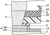
An IDT electrode 3 as a functional electrode is provided on the piezoelectric substrate 2. Electrode pads 4 electrically connected to the IDT electrodes 3 are provided on the piezoelectric substrate 2. The electrode pad 4 has a 1 st electrode layer 4a provided on the piezoelectric substrate 2 and a 2 nd electrode layer 4b provided on the 1 st electrode layer 4 a. Since the electrode pad 4 has 2 electrode layers, the resistance of the electrode pad 4 is low. The electrode pad 4 may be formed of a single electrode layer.
The piezoelectric substrate 2 is provided with a support member 5 having an opening 5 a. The support member 5 surrounds the IDT electrode 3 with an opening 5 a. The support member 5 covers the electrode pad 4. The support member 5 is made of, for example, a suitable resin.
The support member 5 is provided with a cover member 6. The cover member 6 has a 1 st layer 6a provided on the support member 5 and a 2 nd layer 6b provided on the 1 st layer 6 a. The 1 st layer 6a is made of, for example, epoxy resin. This can improve the engagement force between the cover member 6 and the support member 5. The 2 nd layer 6b is made of polyimide or the like, for example. This can improve the strength of the cover member 6. Thus, the cover member 6 is preferably made of resin. In this case, the projecting portion described later can be easily provided. The structure of the cover member 6 is not particularly limited, and the cover member 6 may be a single layer, for example.
The IDT electrode 3 is disposed in a hollow space surrounded by the piezoelectric substrate 2, the support member 5, and the cover member 6.
A projection 7 is provided on an outer peripheral edge 6A of a surface of the cover member 6 on the side opposite to the piezoelectric substrate 2. More specifically, the protruding portion 7 extends from the outer peripheral edge 6A to the side opposite to the piezoelectric substrate 2 side. In the present embodiment, protruding portion 7 is curved so as to extend inward of elastic wave device 1 in a plan view. The protruding portion 7 is provided so as to be located inside the cover member 6 in a plan view. This can prevent the flux adhering to bumps 9 described later from evaporating and scattering outward from cover member 6 during mounting.
As shown in fig. 2, the protruding portion 7 has a frame-like shape in a plan view, and is provided on the entire outer peripheral edge 6A of the surface of the cover member 6 opposite to the piezoelectric substrate 2 side. The projection 7 surrounds the entire outer circumference, thereby effectively suppressing the scattering of the flux. The protruding portion 7 may be provided on at least a part of the outer peripheral edge 6A of the cover member 6.
Returning to fig. 1, in the present embodiment, the protruding portion 7 is integrally provided by the same material as the 2 nd layer 6b of the cover member 6.
The via electrode 8 is provided to penetrate the support member 5 and the cover member 6. One end of the via electrode 8 is connected to the electrode pad 4. A bump 9 is provided for engaging with the other end of the via electrode 8. The bump 9 is made of solder, for example.
As described above, elastic wave device 1 of the present embodiment is an elastic wave device of WLP structure. The IDT electrode 3 is electrically connected to the outside via the electrode pad 4, the via electrode 8, and the bump 9. In addition, the acoustic wave device 1 may be any acoustic wave device having a WLP structure, and the functional electrodes provided on the piezoelectric substrate 2 need not be IDT electrodes.
In the present embodiment, the wiring electrodes 14 provided on the piezoelectric substrate 2 are connected to the electrode pads 4. The wiring electrode 14 is led out to the outside of the support member 5 to the outer peripheral edge of the piezoelectric substrate 2. Wiring electrode 14 is a power supply wiring for forming via electrode 8 in the manufacturing process of acoustic wave device 1 according to the present embodiment. The wiring electrode 14 may not be provided.
The present invention is characterized in that a projection 7 is provided on at least a part of the outer peripheral edge 6A of the surface of the cover member 6 opposite to the piezoelectric substrate 2 side. This can suppress the influence of the flux used in the bump mounting on other electronic components or members and the deterioration of the characteristics. This will be explained below.
Further, in the present embodiment, the flux that can suppress evaporation wraps from the cover member 6 side to the piezoelectric substrate 2 side, and adhesion of the flux to the support member 5 or the piezoelectric substrate 2 can be suppressed. This makes it difficult for the flux to evaporate from the support member 5 or the piezoelectric substrate 2 due to heating after mounting. Therefore, the deterioration of the function of other electronic components, members, and the like due to the flux can be more reliably suppressed.
Furthermore, flux may infiltrate into the hollow space surrounded by the piezoelectric substrate 2, the support member 5, and the cover member 6, and corrode the electrode such as the IDT electrode 3 in the hollow space. For this reason, the characteristics of elastic wave device 1 may deteriorate. In contrast, in the present embodiment, since flux can be prevented from entering the hollow space, deterioration of the characteristics of acoustic wave device 1 can be prevented.
However, when the acoustic wave device 1 includes the wiring electrode 14 as shown in fig. 1, corrosion of the wiring electrode 14 or the like may prevent the sealing property of the IDT electrode 3 in particular. Alternatively, the wiring electrode 14 may be damaged, and the electrode pad 4 may be damaged. In the present embodiment, since the above-described wraparound of the flux is less likely to occur, the flux is also suppressed from reaching the wiring electrodes 14. Damage to elastic wave device 1 is therefore unlikely to occur.
Preferably, as in the present embodiment, the projecting portion 7 is provided on the entire outer peripheral edge 6A of the cover member 6. This facilitates sealing of the evaporated flux in the space surrounded by the cover member 6 and the projection 7. Therefore, the diffusion to the outside of the cover member 6 can be further suppressed, and the wrapping from the cover member 6 side to the piezoelectric substrate 2 side can be further suppressed.
The protruding portion 7 may be provided on at least a part of the outer peripheral edge 6A of the cover member 6. In this case, the evaporated flux is likely to adhere to the surfaces of the protruding portion 7 and the cover member 6 opposite to the piezoelectric substrate 2 side when the flux is directed to the piezoelectric substrate 2 side and the outer side of the cover member 6. The evaporated flux can be suppressed from spreading to the outside of the cover member 6, and can be suppressed from wrapping from the cover member 6 side to the piezoelectric substrate 2 side.
The protruding portion 7 may extend to the side opposite to the piezoelectric substrate 2 side, and the shape of the protruding portion 7 is not particularly limited. For example, the protrusion 27 of the 1 st modification of embodiment 1 shown in fig. 3 linearly extends toward the side opposite to the piezoelectric substrate 2 side. On the other hand, the projection 37 of the 2 nd modification of the 1 st embodiment shown in fig. 4 is bent such that: a part of the outer peripheral edge 6A of the cover member 6 extends outward of the outer peripheral edge 6A and inward in a plan view. In this way, a part of the protruding portion 37 may be located outside the outer peripheral edge 6A in a plan view.
However, although the piezoelectric body is the piezoelectric substrate 2 in embodiment 1, the piezoelectric body may be the piezoelectric thin film 42 as in modification 3 of embodiment 1 shown in fig. 5. For example, the low-speed film 43 may be provided on the surface of the piezoelectric thin film 42 opposite to the surface on which the IDT electrode 3 is provided. The bass member 44 may be provided on the surface of the bass membrane 43 opposite to the piezoelectric film 42.
Here, the low sound velocity film 43 is a film in which the sound velocity of the bulk wave propagating is a low sound velocity compared to the sound velocity of the elastic wave propagating through the piezoelectric thin film 42. The low-speed diaphragm 43 is made of, for example, glass, silicon oxynitride, tantalum oxide, or a material containing silicon oxide and a compound containing fluorine, carbon, or boron as a main component. The material of the low sound velocity film 43 may be any material as long as it is a material having a relatively low sound velocity.
The high sound velocity member 44 is a member that has a higher sound velocity of the body wave propagating than the sound velocity of the elastic wave propagating through the piezoelectric film 42. The high-speed member 44 is made of, for example, a material containing silicon, aluminum nitride, aluminum oxide, silicon carbide, silicon oxynitride, DLC film, diamond, or the like as a main component. The material of the high sound velocity member 44 may be a relatively high sound velocity material.
In this way, when the piezoelectric film 42, the low sound velocity film 43, and the high sound velocity member 44 are provided, the energy of the elastic waves can be effectively blocked.
In addition, the energy of the elastic waves can be confined only by the piezoelectric film 42 and the high-sound-velocity member 44.
The high-sound-velocity member 44 may be a high-sound-velocity film or a high-sound-velocity support substrate.
When high-sound-velocity member 44 is a high-sound-velocity film, elastic wave device 1 may include a support substrate. When elastic wave device 1 includes a support substrate, a high sound velocity film is formed on the support substrate, a low sound velocity film 43 is formed on the high sound velocity film, a piezoelectric thin film 42 is formed on the low sound velocity film 43, and a functional electrode is formed on the piezoelectric thin film 42.
As the high-sound-velocity film, various high-sound-velocity materials such as aluminum nitride, aluminum oxide, silicon carbide, silicon nitride, silicon oxynitride, DLC film, diamond, a medium containing the above materials as a main component, and a medium containing a mixture of the above materials as a main component can be used.
As the high-sound-velocity support substrate, various ceramics such as aluminum nitride, alumina, silicon carbide, silicon nitride, silicon, sapphire, lithium tantalate, lithium niobate, a piezoelectric such as quartz, alumina, zirconia, cordierite, mullite, talc, forsterite, etc., magnesia diamond, a material containing the above-mentioned materials as a main component, or a material containing a mixture of the above-mentioned materials as a main component can be used.
As the support substrate, various ceramics such as silicon, sapphire, lithium tantalate, lithium niobate, a piezoelectric such as quartz, alumina, magnesia, silicon nitride, aluminum nitride, silicon carbide, zirconia, cordierite, mullite, talc, forsterite, etc., a dielectric such as glass, a semiconductor such as gallium nitride, a resin substrate, etc. can be used.
A method of manufacturing acoustic wave device 1 will be described below.
Fig. 6(a) to (c) are front cross-sectional views for explaining a method of manufacturing an elastic wave device according to embodiment 1. Fig. 7(a) to (c) are front cross-sectional views for explaining a method of manufacturing an elastic wave device according to embodiment 1.
As shown in fig. 6(a), a mother substrate 12 is prepared. The mother substrate 12 is not particularly limited, but is made of, for example, LiNbO3Or LiTaO3Or piezoelectric single crystal or suitable piezoelectric ceramics.
Next, a plurality of IDT electrodes 3, electrode pads 4, and power supply lines 14X are formed on the mother substrate 12. The IDT electrode 3, the electrode pad 4, and the power supply line 14X can be formed by, for example, a sputtering method or a vapor deposition method.
Next, as shown in fig. 6(b), a plurality of support members 5 are formed on the mother substrate 12 so as to surround the IDT electrodes 3. The support member 5 can be provided by photolithography or the like, for example. Next, the cover member 16 before cutting is provided on the plurality of support members 5 so as to cover the openings 5a of the plurality of support members 5. At this time, for example, the 1 st layer 16a is provided on the plurality of support members 5, and then the 2 nd layer 16b is laminated on the 1 st layer 16 a. Alternatively, a laminate in which the 1 st layer 16a and the 2 nd layer 16b are laminated may be formed in advance, and the laminate may be provided on the plurality of support members 5.
Next, as shown in fig. 6(c), the through-hole 18 is formed so as to penetrate the support member 5 and the cover member 16 before cutting. The through hole 18 is formed to reach the electrode pad 4. The through-hole 18 can be formed by irradiation of laser light, mechanical cutting, or the like, for example.
Next, as shown in fig. 7(a), the via electrode 8 is formed in the through hole. The via electrode 8 is formed to be connected to the electrode pad 4. In manufacturing elastic wave device 1, via electrode 8 is formed by electrolytic plating using power feeding wiring 14X. The via electrode 8 may be formed by a method other than electrolytic plating. The bump 9 is next provided for bonding to the via electrode 8.
Next, as shown in fig. 7(b), the cover member before cutting is cut by dicing along a dicing line I-I. Thereby obtaining a plurality of cover members 6. At the time of dicing, the outer peripheral edge 6A of the cover member 6 is deformed by contact with a dicing blade, whereby the protruding portion 7 can be formed. In order to increase the processing load on the cover member 6, it is preferable to increase the dicing speed, for example. The protruding portion 7 can thereby be easily formed.
Further, the main curing of the cover member 6 is preferably performed after dicing. When the cover member is not subjected to the main hardening before cutting, the outer peripheral edge 6A of the cover member 6 is easily deformed, and therefore the protruding portion 7 can be further easily formed.
As shown in fig. 7(b), half-cutting of the mother substrate 12 is performed while the cover member before cutting is cut by dicing. At this time, the power supply wiring is cut to form the wiring electrode 14. Next, the cover member 6 side is fixed with a polishing tape, and the surface of the mother substrate 12 opposite to the cover member 6 side is polished. This divides the mother substrate 12 into a plurality of elastic wave devices 1 as shown in fig. 7 (c). The thickness of the piezoelectric substrate 2 can be easily adjusted by the polishing.
In the step shown in fig. 7(b), a plurality of elastic wave devices 1 may be obtained by cutting the mother substrate 12.
The acoustic wave device can be used as a duplexer of a high-frequency front-end circuit, for example. This example is explained below.
Fig. 8 is a configuration diagram of a communication device having a high-frequency front-end circuit. In the figure, the components connected to the high-frequency front-end circuit 230, for example, the antenna element 202 and the RF signal processing circuit (RFIC)203 are also shown. The high-frequency front-end circuit 230 and the RF signal processing circuit 203 constitute a communication device 240. In addition, the communication device 240 may also include a power supply, a CPU, and a display.
The high-frequency front-end circuit 230 includes a switch 225, duplexers 201A and 201B, filters 231 and 232, low- noise amplifier circuits 214 and 224, and power amplifier circuits 234a, 234B, 244a, and 244B. The high-frequency front-end circuit 230 and the communication device 240 in fig. 8 are examples of a high-frequency front-end circuit and a communication device, and are not limited to this configuration.
The duplexer 201A has filters 211, 212. The duplexer 201B includes filters 221 and 222. The duplexers 201A and 201B are connected to the antenna element 202 via a switch 225. The elastic wave devices may be duplexers 201A and 201B, or may be filters 211, 212, 221, and 222. The acoustic wave device may be an acoustic wave resonator constituting the duplexers 201A and 201B and the filters 211, 212, 221, and 222. Further, the acoustic wave device can be applied to a multiplexer including 3 or more filters, such as a triplexer in which antenna terminals of 3 filters are shared and a hexaplexer in which antenna terminals of 6 filters are shared.
That is, the acoustic wave device includes an acoustic wave resonator, a filter, a duplexer, and a multiplexer including 3 or more filters. The multiplexer is not limited to the configuration including both the transmission filter and the reception filter, and may be configured to include only the transmission filter or only the reception filter.
The switch 225 connects the antenna element 202 to a signal path corresponding to a predetermined frequency band in accordance with a control signal from a control unit (not shown), and is constituted by, for example, an SPDT (Single Pole Double Throw) type switch. The number of signal paths connected to the antenna element 202 is not limited to 1, and may be plural. That is, the high-frequency front-end circuit 230 may also correspond to carrier aggregation.
The low noise amplifier circuit 214 is a reception amplifier circuit that amplifies a high frequency signal (here, a high frequency reception signal) via the antenna element 202, the switch 225, and the duplexer 201A and outputs the amplified signal to the RF signal processing circuit 203. The low noise amplifier circuit 224 is a reception amplifier circuit that amplifies the high frequency signal (here, a high frequency reception signal) via the antenna element 202, the switch 225, and the duplexer 201B and outputs the amplified signal to the RF signal processing circuit 203.
The power amplifier circuits 234a and 234b are transmission amplifier circuits that amplify the high-frequency signal (here, a high-frequency transmission signal) output from the RF signal processing circuit 203 and output the amplified signal to the antenna element 202 via the duplexer 201A and the switch 225. The power amplifier circuits 244a and 244B are transmission amplifier circuits that amplify the high-frequency signal (here, a high-frequency transmission signal) output from the RF signal processing circuit 203 and output the amplified signal to the antenna element 202 via the duplexer 201B and the switch 225.
The RF signal processing circuit 203 performs signal processing on the high-frequency reception signal input from the antenna element 202 via the reception signal path by down-conversion or the like, and outputs a reception signal generated by performing the signal processing. The RF signal processing circuit 203 performs signal processing on the transmission signal by up-conversion or the like, and outputs the high-frequency transmission signal generated by the signal processing to the power amplifier circuits 234a, 234b, 244a, and 244 b. The RF signal processing circuit 203 is, for example, an RFIC. The RF signal processing circuit 203 may include a baseband signal processing circuit. The high-frequency front-end circuit 230 may include other circuit elements between the above-described components.
On the other hand, the filters 231 and 232 in the communication device 240 are connected between the RF signal processing circuit 203 and the switch 225 without passing through a low noise amplifier circuit and a power amplifier circuit. The filters 231 and 232 are also connected to the antenna element 202 via the switch 225, similarly to the duplexers 201A and 201B.
According to the high-frequency front-end circuit 230 and the communication device 240 configured as described above, the influence of the flux for bump cleaning on each element can be suppressed by the acoustic wave resonator, the filter, the duplexer, the multiplexer having 3 or more filters, and the like provided with the acoustic wave device of the present invention. And thus deterioration of the functions of the respective elements hardly occurs.
The elastic wave device, the high-frequency front-end circuit, and the communication device according to the embodiments of the present invention have been described above with reference to the embodiments and modifications thereof, but the present invention further includes: another embodiment is realized by combining arbitrary constituent elements of the above-described embodiment and modification example; a modification example in which various modifications that may be made by those skilled in the art are implemented in the above-described embodiment without departing from the spirit of the present invention; various devices incorporating the high-frequency front-end circuit and the communication device according to the present invention.
The present invention is widely used in communication devices such as mobile phones as a filter, a multiplexer applicable to a multiband system, a front-end circuit, and a communication apparatus.
Claims (7)
Applications Claiming Priority (2)
| Application Number | Priority Date | Filing Date | Title |
|---|---|---|---|
| JP2016218138A JP2018078419A (en) | 2016-11-08 | 2016-11-08 | Acoustic wave device, high frequency front end circuit, and communication device |
| JP2016-218138 | 2016-11-08 |
Publications (2)
| Publication Number | Publication Date |
|---|---|
| CN108063603A CN108063603A (en) | 2018-05-22 |
| CN108063603B true CN108063603B (en) | 2021-06-15 |
Family
ID=62064131
Family Applications (1)
| Application Number | Title | Priority Date | Filing Date |
|---|---|---|---|
| CN201710831439.2A Active CN108063603B (en) | 2016-11-08 | 2017-09-14 | Elastic wave device, high-frequency front-end circuit, and communication device |
Country Status (3)
| Country | Link |
|---|---|
| US (1) | US10637434B2 (en) |
| JP (1) | JP2018078419A (en) |
| CN (1) | CN108063603B (en) |
Families Citing this family (5)
| Publication number | Priority date | Publication date | Assignee | Title |
|---|---|---|---|---|
| WO2015022931A1 (en) * | 2013-08-14 | 2015-02-19 | 株式会社村田製作所 | Elastic wave device, electronic component and method for manufacturing elastic wave device |
| CN106464232B (en) * | 2014-06-27 | 2019-09-27 | 株式会社村田制作所 | Elastic wave device and method of making the same |
| KR101958132B1 (en) * | 2015-03-16 | 2019-03-13 | 가부시키가이샤 무라타 세이사쿠쇼 | Seismic wave device and manufacturing method thereof |
| CN114556782B (en) * | 2019-10-24 | 2026-02-24 | 株式会社村田制作所 | Elastic wave device |
| JP2023058393A (en) * | 2021-10-13 | 2023-04-25 | 株式会社村田製作所 | High frequency module and communication apparatus |
Citations (3)
| Publication number | Priority date | Publication date | Assignee | Title |
|---|---|---|---|---|
| CN103384961A (en) * | 2011-03-28 | 2013-11-06 | 京瓷株式会社 | Acoustic wave element and acoustic wave device using same |
| CN104662797A (en) * | 2012-09-25 | 2015-05-27 | 株式会社村田制作所 | Elastic wave device, and method for producing same |
| WO2015199132A1 (en) * | 2014-06-27 | 2015-12-30 | 株式会社村田製作所 | Elastic wave device and method of manufacturing same |
Family Cites Families (10)
| Publication number | Priority date | Publication date | Assignee | Title |
|---|---|---|---|---|
| US7098574B2 (en) * | 2002-11-08 | 2006-08-29 | Toyo Communication Equipment Co., Ltd. | Piezoelectric resonator and method for manufacturing the same |
| JP4517992B2 (en) * | 2005-09-14 | 2010-08-04 | セイコーエプソン株式会社 | Conducting hole forming method, piezoelectric device manufacturing method, and piezoelectric device |
| JP4412286B2 (en) * | 2006-01-20 | 2010-02-10 | セイコーエプソン株式会社 | Manufacturing method of surface acoustic wave device |
| JP5532685B2 (en) | 2009-06-01 | 2014-06-25 | 株式会社村田製作所 | Elastic wave device |
| SG186395A1 (en) * | 2011-05-19 | 2013-01-30 | Taiyo Yuden Kk | Acoustic wave device and module |
| JP5259024B1 (en) * | 2011-08-22 | 2013-08-07 | 京セラ株式会社 | Elastic wave device and electronic component |
| JP2013102344A (en) * | 2011-11-08 | 2013-05-23 | Nippon Dempa Kogyo Co Ltd | Electronic component package |
| CN103281050A (en) * | 2013-06-17 | 2013-09-04 | 天津大学 | Film bulk acoustic wave filter |
| JP6256036B2 (en) * | 2014-01-21 | 2018-01-10 | セイコーエプソン株式会社 | Vibrator, oscillator, electronic device, and moving object |
| CN105337586B (en) * | 2015-12-03 | 2018-04-17 | 天津大学 | Lamb wave resonator |
-
2016
- 2016-11-08 JP JP2016218138A patent/JP2018078419A/en active Pending
-
2017
- 2017-09-14 CN CN201710831439.2A patent/CN108063603B/en active Active
- 2017-10-04 US US15/724,567 patent/US10637434B2/en active Active
Patent Citations (3)
| Publication number | Priority date | Publication date | Assignee | Title |
|---|---|---|---|---|
| CN103384961A (en) * | 2011-03-28 | 2013-11-06 | 京瓷株式会社 | Acoustic wave element and acoustic wave device using same |
| CN104662797A (en) * | 2012-09-25 | 2015-05-27 | 株式会社村田制作所 | Elastic wave device, and method for producing same |
| WO2015199132A1 (en) * | 2014-06-27 | 2015-12-30 | 株式会社村田製作所 | Elastic wave device and method of manufacturing same |
Also Published As
| Publication number | Publication date |
|---|---|
| JP2018078419A (en) | 2018-05-17 |
| CN108063603A (en) | 2018-05-22 |
| US20180131345A1 (en) | 2018-05-10 |
| US10637434B2 (en) | 2020-04-28 |
Similar Documents
| Publication | Publication Date | Title |
|---|---|---|
| US10250222B2 (en) | Electronic device | |
| CN108063603B (en) | Elastic wave device, high-frequency front-end circuit, and communication device | |
| JP6556663B2 (en) | Elastic wave device | |
| CN111418152B (en) | Elastic wave device, high-frequency front-end circuit, and communication device | |
| KR102253460B1 (en) | Acoustic wave device, high frequency front end circuit and communication device | |
| JP2017169139A (en) | Elastic wave device | |
| US11695389B2 (en) | Acoustic wave device, front-end circuit, and communication apparatus | |
| JP6791390B2 (en) | Elastic wave device, high frequency front end circuit and communication device | |
| US11515856B2 (en) | Acoustic wave device, front-end circuit, and communication apparatus | |
| JP6756411B2 (en) | Elastic wave device, high frequency front end circuit and communication device | |
| CN111566933B (en) | Elastic wave device, high-frequency front-end circuit, communication device, and method for manufacturing elastic wave device | |
| JP2019145886A (en) | Acoustic wave device, high-frequency front-end circuit, and communication device | |
| JP7465515B1 (en) | Acoustic Wave Devices | |
| JP2022157185A (en) | High-frequency module and communication device |
Legal Events
| Date | Code | Title | Description |
|---|---|---|---|
| PB01 | Publication | ||
| PB01 | Publication | ||
| SE01 | Entry into force of request for substantive examination | ||
| SE01 | Entry into force of request for substantive examination | ||
| GR01 | Patent grant | ||
| GR01 | Patent grant |