CN108028605B - Converter with hold-up operation - Google Patents
Converter with hold-up operation Download PDFInfo
- Publication number
- CN108028605B CN108028605B CN201680053678.3A CN201680053678A CN108028605B CN 108028605 B CN108028605 B CN 108028605B CN 201680053678 A CN201680053678 A CN 201680053678A CN 108028605 B CN108028605 B CN 108028605B
- Authority
- CN
- China
- Prior art keywords
- terminal
- converter
- transistor
- resonant
- voltage
- Prior art date
- Legal status (The legal status is an assumption and is not a legal conclusion. Google has not performed a legal analysis and makes no representation as to the accuracy of the status listed.)
- Active
Links
Images




Classifications
-
- H—ELECTRICITY
- H02—GENERATION; CONVERSION OR DISTRIBUTION OF ELECTRIC POWER
- H02M—APPARATUS FOR CONVERSION BETWEEN AC AND AC, BETWEEN AC AND DC, OR BETWEEN DC AND DC, AND FOR USE WITH MAINS OR SIMILAR POWER SUPPLY SYSTEMS; CONVERSION OF DC OR AC INPUT POWER INTO SURGE OUTPUT POWER; CONTROL OR REGULATION THEREOF
- H02M3/00—Conversion of DC power input into DC power output
- H02M3/22—Conversion of DC power input into DC power output with intermediate conversion into AC
- H02M3/24—Conversion of DC power input into DC power output with intermediate conversion into AC by static converters
- H02M3/28—Conversion of DC power input into DC power output with intermediate conversion into AC by static converters using discharge tubes with control electrode or semiconductor devices with control electrode to produce the intermediate AC
- H02M3/325—Conversion of DC power input into DC power output with intermediate conversion into AC by static converters using discharge tubes with control electrode or semiconductor devices with control electrode to produce the intermediate AC using devices of a triode or a transistor type requiring continuous application of a control signal
- H02M3/335—Conversion of DC power input into DC power output with intermediate conversion into AC by static converters using discharge tubes with control electrode or semiconductor devices with control electrode to produce the intermediate AC using devices of a triode or a transistor type requiring continuous application of a control signal using semiconductor devices only
- H02M3/33569—Conversion of DC power input into DC power output with intermediate conversion into AC by static converters using discharge tubes with control electrode or semiconductor devices with control electrode to produce the intermediate AC using devices of a triode or a transistor type requiring continuous application of a control signal using semiconductor devices only having several active switching elements
- H02M3/33576—Conversion of DC power input into DC power output with intermediate conversion into AC by static converters using discharge tubes with control electrode or semiconductor devices with control electrode to produce the intermediate AC using devices of a triode or a transistor type requiring continuous application of a control signal using semiconductor devices only having several active switching elements having at least one active switching element at the secondary side of an isolation transformer
- H02M3/33592—Conversion of DC power input into DC power output with intermediate conversion into AC by static converters using discharge tubes with control electrode or semiconductor devices with control electrode to produce the intermediate AC using devices of a triode or a transistor type requiring continuous application of a control signal using semiconductor devices only having several active switching elements having at least one active switching element at the secondary side of an isolation transformer having a synchronous rectifier circuit or a synchronous freewheeling circuit at the secondary side of an isolation transformer
-
- H—ELECTRICITY
- H02—GENERATION; CONVERSION OR DISTRIBUTION OF ELECTRIC POWER
- H02M—APPARATUS FOR CONVERSION BETWEEN AC AND AC, BETWEEN AC AND DC, OR BETWEEN DC AND DC, AND FOR USE WITH MAINS OR SIMILAR POWER SUPPLY SYSTEMS; CONVERSION OF DC OR AC INPUT POWER INTO SURGE OUTPUT POWER; CONTROL OR REGULATION THEREOF
- H02M3/00—Conversion of DC power input into DC power output
- H02M3/22—Conversion of DC power input into DC power output with intermediate conversion into AC
- H02M3/24—Conversion of DC power input into DC power output with intermediate conversion into AC by static converters
- H02M3/28—Conversion of DC power input into DC power output with intermediate conversion into AC by static converters using discharge tubes with control electrode or semiconductor devices with control electrode to produce the intermediate AC
- H02M3/325—Conversion of DC power input into DC power output with intermediate conversion into AC by static converters using discharge tubes with control electrode or semiconductor devices with control electrode to produce the intermediate AC using devices of a triode or a transistor type requiring continuous application of a control signal
- H02M3/335—Conversion of DC power input into DC power output with intermediate conversion into AC by static converters using discharge tubes with control electrode or semiconductor devices with control electrode to produce the intermediate AC using devices of a triode or a transistor type requiring continuous application of a control signal using semiconductor devices only
- H02M3/33507—Conversion of DC power input into DC power output with intermediate conversion into AC by static converters using discharge tubes with control electrode or semiconductor devices with control electrode to produce the intermediate AC using devices of a triode or a transistor type requiring continuous application of a control signal using semiconductor devices only with automatic control of the output voltage or current, e.g. flyback converters
-
- H—ELECTRICITY
- H02—GENERATION; CONVERSION OR DISTRIBUTION OF ELECTRIC POWER
- H02M—APPARATUS FOR CONVERSION BETWEEN AC AND AC, BETWEEN AC AND DC, OR BETWEEN DC AND DC, AND FOR USE WITH MAINS OR SIMILAR POWER SUPPLY SYSTEMS; CONVERSION OF DC OR AC INPUT POWER INTO SURGE OUTPUT POWER; CONTROL OR REGULATION THEREOF
- H02M7/00—Conversion of AC power input into DC power output; Conversion of DC power input into AC power output
- H02M7/02—Conversion of AC power input into DC power output without possibility of reversal
- H02M7/04—Conversion of AC power input into DC power output without possibility of reversal by static converters
- H02M7/12—Conversion of AC power input into DC power output without possibility of reversal by static converters using discharge tubes with control electrode or semiconductor devices with control electrode
- H02M7/21—Conversion of AC power input into DC power output without possibility of reversal by static converters using discharge tubes with control electrode or semiconductor devices with control electrode using devices of a triode or transistor type requiring continuous application of a control signal
- H02M7/217—Conversion of AC power input into DC power output without possibility of reversal by static converters using discharge tubes with control electrode or semiconductor devices with control electrode using devices of a triode or transistor type requiring continuous application of a control signal using semiconductor devices only
-
- H—ELECTRICITY
- H02—GENERATION; CONVERSION OR DISTRIBUTION OF ELECTRIC POWER
- H02M—APPARATUS FOR CONVERSION BETWEEN AC AND AC, BETWEEN AC AND DC, OR BETWEEN DC AND DC, AND FOR USE WITH MAINS OR SIMILAR POWER SUPPLY SYSTEMS; CONVERSION OF DC OR AC INPUT POWER INTO SURGE OUTPUT POWER; CONTROL OR REGULATION THEREOF
- H02M1/00—Details of apparatus for conversion
- H02M1/0048—Circuits or arrangements for reducing losses
- H02M1/0054—Transistor switching losses
- H02M1/0058—Transistor switching losses by employing soft switching techniques, i.e. commutation of transistors when applied voltage is zero or when current flow is zero
-
- H—ELECTRICITY
- H02—GENERATION; CONVERSION OR DISTRIBUTION OF ELECTRIC POWER
- H02M—APPARATUS FOR CONVERSION BETWEEN AC AND AC, BETWEEN AC AND DC, OR BETWEEN DC AND DC, AND FOR USE WITH MAINS OR SIMILAR POWER SUPPLY SYSTEMS; CONVERSION OF DC OR AC INPUT POWER INTO SURGE OUTPUT POWER; CONTROL OR REGULATION THEREOF
- H02M1/00—Details of apparatus for conversion
- H02M1/32—Means for protecting converters other than automatic disconnection
- H02M1/325—Means for protecting converters other than automatic disconnection with means for allowing continuous operation despite a fault, i.e. fault tolerant converters
-
- Y—GENERAL TAGGING OF NEW TECHNOLOGICAL DEVELOPMENTS; GENERAL TAGGING OF CROSS-SECTIONAL TECHNOLOGIES SPANNING OVER SEVERAL SECTIONS OF THE IPC; TECHNICAL SUBJECTS COVERED BY FORMER USPC CROSS-REFERENCE ART COLLECTIONS [XRACs] AND DIGESTS
- Y02—TECHNOLOGIES OR APPLICATIONS FOR MITIGATION OR ADAPTATION AGAINST CLIMATE CHANGE
- Y02B—CLIMATE CHANGE MITIGATION TECHNOLOGIES RELATED TO BUILDINGS, e.g. HOUSING, HOUSE APPLIANCES OR RELATED END-USER APPLICATIONS
- Y02B70/00—Technologies for an efficient end-user side electric power management and consumption
- Y02B70/10—Technologies improving the efficiency by using switched-mode power supplies [SMPS], i.e. efficient power electronics conversion e.g. power factor correction or reduction of losses in power supplies or efficient standby modes
Landscapes
- Engineering & Computer Science (AREA)
- Power Engineering (AREA)
- Dc-Dc Converters (AREA)
Abstract
The present invention provides a converter with hold-up operation, comprising: a half-bridge circuit comprising a first transistor and a second transistor connected in series, the half-bridge circuit being connected in parallel with the voltage input and comprising a node connected to both the first transistor and the second transistor; a resonant inductor connected to the half-bridge circuit and the primary winding of the transformer; a resonant capacitor connected to the half-bridge circuit and the primary winding; a third transistor having a first terminal connected to the half-bridge circuit and a second terminal directly connected to the first terminal of the resonant inductor; and a rectification stage connected to the secondary winding of the transformer and including a first synchronous rectifier and a second synchronous rectifier. The rectification stage does not use a discrete diode to provide rectification and the third transistor is turned on and off to maintain the output voltage level during the voltage boost operation.
Description
Technical Field
The present invention relates to devices such as high efficiency power supplies. More particularly, the present invention relates to a resonant converter that performs a hold-up operation.
Background
In devices such as telecommunications power supplies, maintenance issues should be considered. When input AC power is interrupted or lost, the output voltage of a Power Factor Correction (PFC) stage continuously drops as the output capacitor discharges. The hold time refers to the time that the power supply can maintain the output voltage level within its rated output voltage range after the input AC power is interrupted or lost. The problem of retention is how to increase the retention time as much as possible.
LLC series resonant converters have been used because the primary switch can use Zero Voltage Switching (ZVS) and because the rectifier diodes have no reverse recovery problem. Although conventional LLC series resonant converters can achieve high efficiency, they do not solve the hold-up problem.
A two-stage AC/DC converter is shown in fig. 1. The circuit shown in fig. 1 can be used with known converters and converters according to preferred embodiments of the invention. Two-stage AC/DC converters include a Power Factor Correction (PFC) stage and a DC/DC stage and have been widely used for many industrial applications. Fig. 1 shows a block diagram of a two-stage AC/DC converter. The PFC stage can realize high power factor and output voltage VbusThe requirements of the DC/DC stage can be met. LLC series resonant converter topologies are used to achieve high efficiency and high power density because the topology can use ZVS on the primary side and Zero Capacitance Switching (ZCS) on the secondary side. Synchronous Rectifiers (SR) are widely used in low output voltage applications to reduce the conduction losses of the output rectifier and thereby improve efficiency. Since the LLC series-resonant converter is a current-fed topology and has no output inductor, the voltage stress on the output rectifier is much lower than in conventional voltage-fed topologies. A low voltage rated Metal Oxide Semiconductor Field Effect Transistor (MOSFET) may be used as the synchronous rectifier SR to achieve high efficiency. Therefore, an LLC series resonant converter with synchronous rectifier SR is an ideal topology to achieve high efficiency in low output voltage applications. After loss of the AC voltage, the output voltage should be held for a period of time, which is called holdTime periods, as shown in fig. 2. During the hold period, the storage capacitor CbusSupplying power to the LLC series resonant converter. Therefore, the DC/DC stage should provide sufficient voltage gain to keep the output voltage of the LLC series-resonant converter stable.
LLC series resonant converters regulate the output voltage by lowering the switching frequency, assuming the converter operates in the inductive region. LLC series resonant converters with a wide input voltage range should have small magnetizing inductance to achieve high peak gain. Such a small magnetizing inductance results in large conduction losses on the primary side. Therefore, it is difficult to obtain an optimized design having a wide input voltage range and realizing a flat efficiency curve. In order to obtain good performance during operation and to meet the voltage gain requirements during the hold-up period, many methods for hold-up operation have been developed based on LLC series resonant converters.
A first known method of providing a hold-up operation uses an additional secondary side winding to increase the number of secondary turns during the hold-up operation. The additional winding is connected in series with the secondary winding of the transformer. Diodes and switches may be used to connect and disconnect additional windings.
Fig. 3 shows a prior art LLC converter using a first known method of providing hold-up operation. Such a prior art converter comprises a primary side and a secondary side. The primary side being at the DC input VinAnd the converter side between the transformers. On the secondary side of the transformer and the output voltage VOOn the converter side in between.
The primary circuit includes a primary switch Q1,Q2Resonant inductor LrA resonant capacitor CrAnd an inductor Lm. Primary switch Q1,Q2Is connected to the DC input terminal Vin. Resonant inductor LrAnd a resonant capacitor CrAre connected in series with each other and connected between the primary winding of the transformer T and the primary switch Q1,Q2Between nodes. Inductor LmConnected in parallel across the primary winding of the transformer T. Voltage VLrIs a resonant inductor LrVoltage across, and current iLrIs a streamOver-resonant inductor LrThe current of (2). Voltage VCrIs a resonant capacitor CrThe voltage across the terminals. Current iLmIs flowing through the inductor LmThe current of (2). The secondary circuit comprises a rectifier diode D arranged in a bridge1,D2,D3,D4Resistance ROAnd an output capacitor CO. Current IrectIs the current from the rectifier bridge. Resistance RORepresenting the output resistance. The above components are typical components of LLC converters.
The secondary circuit further comprises an auxiliary winding Na. Series-connected diodes D5And switch Q3Connected to the auxiliary winding NaAnd an output terminal. By adding secondary turns during hold-up operation, the converter can achieve higher voltage gain than a conventional LLC converter. However, the additional transformer winding means a larger transformer size and is provided with a switch Q3And a diode D5Resulting in lower power density and higher cost.
"LLC series resonant converter with auxiliary hold-up time compensation circuit" as authored by Kim et al, proc.ieee Energy converters.congr.expo.asia; 2011; as shown in fig. 3 and 4 on page 628-633, during normal operation the additional switches are open and the additional windings are not connected. During the hold operation, the additional switch is switched on and the winding is connected. In this way, the number of secondary side turns increases. The disadvantage of this approach is that the turns ratio does not change smoothly, but rather, such as from 17: 1 to 16: 1. therefore, when the winding ratio changes, the output voltage will jump. Adding additional transformer windings increases the size of the transformer, and additional diodes and additional switches decrease power density and increase complexity.
Fig. 4 shows a prior art LLC converter with a secondary auxiliary circuit providing ZVS to the transformer. The secondary circuit comprising only two rectifier diodes D1,D2And comprises auxiliary windings each connected to an inductor connected in series with a diode D4 or D5, and comprising a switch and a diode D connected to a rectifier1,D2Of (2) a diode. Although this known converter can achieve higher voltage gain, the secondary auxiliary circuit of the converter has many bulky components and is not suitable for low output voltage applications requiring synchronous rectifier MOSFETs.
A second known method of providing hold operation uses a Pulse Width Modulation (PWM) control scheme to increase the primary current. This second known method can increase the voltage gain without using any additional components, but requires changing the control scheme from Pulse Frequency Modulation (PFM) control to PWM control during the hold operation. Thereby achieving high voltage gain while maintaining high power density. The improved topology using the auxiliary switch may solve the above discussed drawback of the first known method of output voltage jump at a change of the winding ratio. In a second known method, additional switches are controlled in the PWM mode. By adjusting the duty ratio, the output voltage can be smoothly changed.
The auxiliary switches operate under PWM control and the main switches of the converter also operate under PFM during hold-up operation. However, the second method is only applicable to diode rectifiers, because the second known method will short-circuit when a synchronous rectifier is used instead of a diode rectifier. Therefore, the second method is not suitable for low voltage, high current output applications.
Fig. 5 shows a prior art converter using a second known method of providing hold-up operation. An asymmetric PWM control method is used. As shown in fig. 5, the primary switch Q1,Q2Have different lengths. The converter in fig. 5 does not require additional circuitry. The voltage gain can only be increased using an asymmetric PWM control method, but it is difficult to obtain sufficient gain for the hold-up operation as explained in "asymmetric PWM control scheme during hold-up time of LLC resonant converters" by Kim et al (IEEE trans. ind. electron.; volume 59, No. 7; month 7 2012; page 2992-.
Fig. 6 and 7 show two existing LLC converters using a boost PWM control method. The boost PWM control method operates with a narrow variation range of the switching frequency over a wide input voltage range. In addition, PWM control is performed due to boostingThe manufacturing method decouples the normal operation and the hold operation, so it is possible to obtain an optimal design during normal operation. Since the LLC converter performs PFM during normal operation, changing the switching frequency to regulate the output voltage, and performs PWM during hold-up operation, fixing the switching frequency and changing the duty cycle to regulate the output voltage, the normal operation and hold-up operation of the LLC converter are decoupled. Therefore, the boost PWM control works only during the hold operation, allowing the decoupling of the normal operation and the hold operation. But the boost PWM control method is not suitable for low output voltage applications with synchronous rectifiers SR due to the risk of short circuits. In fig. 6 and 7, two secondary rectifier diodes and two synchronous rectifiers SR are used1,SR2. If both diodes are replaced with synchronous rectifiers, a short circuit condition can occur.
Fig. 8 shows another known converter having four rectifying diodes and an inductor L in resonance with itrAnd a resonant capacitor CrWith switch Q on the primary side of the parallel connection3. This boost PWM control method also suffers from short circuit conditions if synchronous rectifier MOSFETs are used in place of the rectifier diodes. Once switched Q2,Q3On, the primary side of the transformer is short circuited. And a rectifying diode is required in the secondary circuit.
Disclosure of Invention
To overcome the above problems, preferred embodiments of the present invention provide an improved LLC resonant converter and method of operation during hold-up operation, which is suitable for low voltage, high current applications using synchronous rectifiers on the secondary side, and uses only one additional switch (or one switch and one diode), which adds little cost.
According to a preferred embodiment of the invention, the converter comprises: a voltage input terminal; a transformer including a primary winding and a secondary winding; a voltage output terminal; a primary circuit connected to the voltage input and the primary winding, the primary circuit comprising a half-bridge circuit having a first transistor and a second transistor connected in series, the half-bridge circuit being connected in parallel with the voltage input and comprising: a third transistor connected to a node of both the first transistor and the second transistor, a resonant inductor connected to the half-bridge circuit and the primary winding, a resonant capacitor connected to the half-bridge circuit and the primary winding, and a first terminal connected to the half-bridge circuit and a second terminal directly connected to a first terminal of the resonant inductor; and a secondary circuit connected to the secondary winding and the voltage output, the secondary circuit comprising a rectification stage connected to the secondary winding and having a first synchronous rectifier and a second synchronous rectifier. The rectification stage provides rectification without using a discrete diode and turns the third transistor on and off to maintain the output voltage level during the voltage boost operation.
The converter further preferably comprises a diode connected to the third transistor.
Preferably, the second terminal of the third transistor is also directly connected to the first terminal of the resonant capacitor, the first terminal of the resonant inductor is connected with the first terminal of the resonant capacitor, such that the resonant capacitor is connected to the half-bridge circuit through the resonant inductor, the second terminal of the resonant inductor is connected to a node of the half-bridge circuit, and the second terminal of the resonant capacitor is connected to the primary winding.
The first terminal of the third transistor is also preferably connected to the negative terminal of the voltage input terminal. The primary winding is preferably directly connected to the negative terminal of the input voltage or to the positive terminal of the input voltage.
The first terminal of the third transistor is also preferably connected to the positive terminal of the voltage input terminal. The primary winding is preferably directly connected to the negative terminal of the input voltage or to the positive terminal of the input voltage.
Preferably, the second terminal of the third transistor is also directly connected to the first terminal of the resonance capacitor, the first terminal of the resonance inductor is connected with the first terminal of the resonance capacitor, so that the resonance capacitor is connected to the half-bridge circuit through the resonance inductor, the second terminal of the resonance inductor is connected to the negative terminal of the input voltage, and the second terminal of the resonance capacitor is connected to the primary winding.
The first terminal of the third transistor is also preferably connected to the positive terminal of the voltage input terminal. The converter further preferably comprises a diode connected to the third transistor.
Preferably, the second terminal of the third transistor is also directly connected to the first terminal of the resonant capacitor, the first terminal of the resonant inductor is connected with the first terminal of the resonant capacitor, so that the resonant capacitor is connected to the half-bridge circuit through the resonant inductor, the second terminal of the resonant inductor is connected to the positive terminal of the input voltage, and the second terminal of the resonant capacitor is connected to the primary winding.
The first terminal of the third transistor is also preferably connected to the negative terminal of the voltage input terminal. The converter further preferably comprises a diode connected to the third transistor.
Preferably, the second terminal of the third transistor is also connected to the primary winding, the first terminal of the resonance capacitor is connected to the node of the half-bridge circuit, and the second terminal of the resonance capacitor is connected to the primary winding.
Preferably, the second terminal of the resonant inductor is connected to a negative terminal of the input voltage, and the first terminal of the third transistor is also connected to a positive terminal of the input voltage. Preferably, the second terminal of the resonant inductor is connected to a positive terminal of the input voltage, and the first terminal of the third transistor is also connected to a negative terminal of the input voltage.
When the input voltage is lower than the threshold voltage, the voltage boosting operation is preferably performed during the holding period. During voltage boost operation, the resonant capacitor preferably increases the energy of the resonant inductor to maintain the output voltage level.
The above and other features, elements, features, steps and advantages of the present invention will become more apparent from the following detailed description of preferred embodiments of the present invention with reference to the accompanying drawings.
Drawings
Fig. 1 shows a circuit with a PFC stage and a DC/DC stage.
Fig. 2 shows voltage waveforms during normal period operation and during hold period operation.
Fig. 3-8 show a prior art converter.
Fig. 9-18 show converters according to first to tenth preferred embodiments of the present invention.
Fig. 19 shows waveforms during normal operation.
Fig. 20 shows waveforms during the hold operation.
Fig. 21-25 illustrate the operation of the converter according to the tenth preferred embodiment of the present invention illustrated in fig. 18.
Fig. 26 shows the relative gain of the converter as a function of the duty cycle of the additional switches.
Fig. 27-29 show waveforms of the converter tested at a load current of 25A.
Fig. 30-32 show waveforms of the converter tested at a load current of 15A.
Detailed Description
Preferred embodiments of the present invention provide a Half Bridge (HB) LLC converter with increased voltage gain. During normal operation, i.e. when the input voltage is within the nominal input voltage range, the converter can operate with maximum efficiency. When the input voltage is low, the additional switch starts to operate in the PWM mode to increase the energy transferred from the DC input to the resonant tank to be transferred to the output, thereby increasing the voltage gain. This is particularly suitable for the hold operation. Since the normal operation and the holding operation are decoupled, the switching frequency variation range is not wide, so that high efficiency can be achieved. The additional switch may be connected in series with a diode that disconnects the branch of the additional switch, thereby charging the parasitic capacitor of the additional switch.
During normal operation, the switches attached in the converter according to the preferred embodiment of the invention are not turned on, and the converter operates like a conventional half bridge LLC converter. The output voltage is controlled by adopting a switching frequency control mode. The switching frequency can be designed around the resonance frequency and can therefore be optimized. When the input voltage is low, the converter may operate in a voltage boost mode, the primary switch operates at a minimum switching frequency, and the additional switch operates in a PWM mode to increase the energy transferred from the input source to the resonant tank, thereby increasing the voltage gain. The holding period is a period in which the input voltage is low.
Fig. 9 shows a converter according to a first preferred embodiment of the invention. The converter shown in fig. 9 may be used as the DC/DC stage in fig. 1. DC input V in FIG. 9inCorresponding to the capacitor C in fig. 1busVoltage V onbus。
The primary circuit includes a primary switch Q1,Q2Resonant inductor LrA resonant capacitor CrDiode D1Q switch3And an inductor Lm. Primary switch Q1,Q2Is connected to the DC input terminal Vin. Resonant inductor LrAnd a resonant capacitor CrAre connected in series with each other and connected between the primary winding of the transformer T and the primary switch Q1,Q2Between nodes. Diode D1And switch Q3Are connected in series with each other and at an input voltage VinNegative terminal of and resonant inductor LrAnd a resonant capacitor CrBetween nodes. Inductor LmConnected in parallel across the primary winding of the transformer T. The transformer winding ratio is N. Voltage VHBIs the voltage of the half bridge. Voltage VLrIs a resonant inductor LrVoltage across, and current iLrIs flowing through the resonant inductor LrThe current of (2). Voltage VCrIs a resonant capacitor CrThe voltage across the terminals. Voltage VmIs the voltage across the primary winding of the transformer T, and the current iLmIs flowing through the inductor LmThe current of (2). Current iQ3Is passed through the auxiliary switch Q3The current of (2).
The secondary circuit comprising a synchronous rectifier SR1,SR2Resistance ROAnd a capacitor CO. Synchronous rectifier SR1,SR2Connected to the secondary winding of the transformer T and forming a rectifying stage which at an output voltage VOTo provide a rectified output. The rectification stage does not include or use a diode to provide a rectified output. Resistance RORepresenting the resistance of the output terminal. Current IrectIs the current from the rectifier stage.
In fig. 9, the converter includes a switch Q3(or a switch Q)3And a diode D1). Switch Q3Only during the hold operation. In normal operation, as the input voltage decreases, the primary switch Q1,Q2The switching frequency of (2) is reduced. Once the switching frequency is reduced to a set minimum frequency, the Q switch3Is increased from zero while the primary switch Q is switched on1,Q2The switching frequency of (a) is fixed, thereby starting the hold operation. Thus, the converter can be designed according to normal operation. When the switch Q3When turned on, the inductor LrCan be charged and transfer a large amount of energy to the secondary side. Thus, the gain increases. When the DC input end VinWhen switched off, is fed into a DC bus capacitor (not shown, but possibly connected to a DC input VinParallel connection) and auxiliary switch Q3To resonant inductor LrCharging is carried out so that the output voltage V isORemain unchanged. Thus, the retention time may be increased.
Because of the capacitor CrConnected between transformer T and charging circuit, i.e. via a switch Q3Or a switch Q3And a diode D4Connected, the DC/DC converter is suitable for synchronous rectifier applications. In synchronous rectifier applications, short circuits on the primary side of the transformer must be avoided because the synchronous rectifier can provide bi-directional current. Known auxiliary switching methods increase the energy of the inductor and make the output voltage constant by short-circuiting the transformer during the holding operation. Shorting the transformer is only suitable for diode rectifier applications. In synchronous rectifier applications, a resonant capacitor in series with the transformer may add an inductor L during hold-up operationrSo that the output voltage is constant. The resonant capacitor does not directly short circuit the primary side of the transformer, and is suitable for diode rectifier applications and synchronous rectifier applications.
Except for the switch Q3And a diode D1Except for the change of position, the transducer according to the second preferred embodiment shown in fig. 10 is similar to the transducer of the first preferred embodiment of fig. 9. In FIG. 10, switch Q3And a diode D1Still connected in series, but in a different manner. Switch Q3And a diode D1Connected to a resonant inductor LrAnd a resonant capacitor CrAt a node other than the input voltage VinNegative terminal of (2), switch Q3And a diode D1Connected to an input voltage VinThe positive electrode terminal of (1).
Except for the resonant inductor LrAnd a resonant capacitor CrNot directly connected in series, without the need for diode D1And switch Q3The converters according to the third and fourth preferred embodiments shown in fig. 11 and 12 are similar to the converters according to the first and second preferred embodiments shown in fig. 9 and 10, except for the different connection ways. If the switching voltage is negative, the auxiliary switch Q3The body diode of (1) cannot be turned on. For half-bridge topology, resonant capacitor CrWith half the DC voltage plus the high frequency AC voltage and no negative voltage in fig. 11 and 12. Therefore, the diode D is not required in fig. 11 and 121However, in fig. 9 and 10, a diode D is required1. Current iTIs the current flowing through the primary winding of the transformer. Current isen1Is a synchronous rectifier S1The current of (2). Current isen2Is a synchronous rectifier S2The current of (2). Resistance RfAnd a capacitor CfIs configured to output a voltage VOThe filter of (1).
In fig. 11, a resonant inductor LrConnected to an input voltage VinAnd switch Q3Connected to an input voltage VinThe positive electrode terminal of (1).
In fig. 12, a resonant inductor LrConnected to an input voltage VinAnd switch Q3Connected to an input voltage VinThe negative electrode terminal of (1). The converter of fig. 12 is most cost effective and the driver circuit required is least complex because there is no auxiliary diode compared to fig. 9 and 10, and the auxiliary switch Q of fig. 123And switch Q2Is grounded in common, which means drivingThe circuit is simple and the cost is low.
Except for diodes D connected in series1And switch Q3Inductor LmAnd the transformers are all connected to an input voltage VinExcept for the positive terminal, the converter according to the fifth embodiment shown in fig. 13 is similar to the converter according to the first preferred embodiment shown in fig. 9.
Except for the inductor LmAnd the transformer are connected to the input voltage VinExcept for the positive terminal, the converter according to the sixth preferred embodiment shown in fig. 14 is similar to the converter according to the first preferred embodiment shown in fig. 9.
Except for the resonant inductor LrAnd a resonant capacitor CrConnected in series directly at an input voltage VinExcept between the negative terminal and the transformer, the converter according to the seventh preferred embodiment shown in fig. 15 is similar to the converter according to the third preferred embodiment shown in fig. 11.
Except for the resonant inductor LrAnd a resonant capacitor CrConnected in series directly at an input voltage VinExcept between the negative terminal and the transformer, the converter according to the eighth preferred embodiment shown in fig. 16 is similar to the converter according to the fourth preferred embodiment shown in fig. 12.
Except that the diode D is not used1Except that the converter according to the ninth preferred embodiment shown in fig. 17 is similar to the converter according to the seventh preferred embodiment shown in fig. 15.
Except that the diode D is not used1Except that the converter according to the tenth preferred embodiment shown in fig. 18 is similar to the converter according to the eighth preferred embodiment shown in fig. 16.
As with the converter of fig. 12, the converter of fig. 18 is the most cost effective and the least complex driver circuit is required because there is no auxiliary diode and the switch Q is2And Q3Which means that the driving circuit is simple and low cost.
The operation of the converter according to the tenth preferred embodiment is discussed below. Other preferred embodiments operate in a similar manner. FIG. 1 shows a schematic view of aFig. 9 and 20 show waveforms during normal operation and during a holding operation (i.e., voltage boosting operation). During normal operation, the operation of the converter is similar to known converters. FIG. 19 shows waveforms during normal operation, during which the switch Q is switched3And (5) disconnecting. FIG. 20 shows waveforms during a hold operation, during which the switch Q is switched3On and off. Fig. 21-25 show the converter during hold-up operation.
Fig. 21 shows the converter during mode 1 (M1). Switch Q2,Q3At t0And (4) switching on. Due to application to the resonant inductor LrPositive input voltage V ofinResonant current iLrIncreasing linearly. Magnetic inductor LmBy a resonant capacitor CrAnd (6) charging. Current flows through switch Q3And switch Q2The body diode of (1).
Fig. 22 shows the converter during mode 2 (M2). Switch Q3At t1And is disconnected. A large resonant current flows through the resonant capacitor CrMagnetic inductor LmTransformer and switch Q2. Large rectifier current through synchronous rectifier SR2To an output capacitor COAnd (6) charging.
Fig. 23 shows the converter during mode 3 (M3). At time t2At this time, the current flowing through the secondary side of the transformer reaches zero as shown in fig. 20. The converter enters an idle mode in which no power is transferred from the input to the output. Three elements (resonant inductor L)rA resonant capacitor CrAnd magnetic inductor Lm) And (4) resonating.
Fig. 24 shows the converter during mode 4 (M4). At time t3Time, switch Q2Is turned off and switch Q is turned on1And (4) switching on. Primary side voltage VmIs clamped to N x Vo(ii) a The incoming energy is transferred to the secondary side. The operation during M4 is similar to known converters.
Fig. 25 shows the converter during mode 5 (M5). At time t4The current flowing through the secondary side of the transformer reaches zero. The converter enters an idle mode in whichNo power is transmitted from the input to the output. Three elements (resonant inductor L)rA resonant capacitor CrAnd magnetic inductor Lm) And (4) resonating.
The converter has two different input-to-output voltage conversion ratios depending on the operating state of the converter. During normal operation, the converter has the same operating characteristics as the known converter. FIG. 26 shows that the switching frequency remains at the minimum frequency fminAnalog relationship of voltage gain in time and duty cycle of switch Q3. Switch Q3Is defined as the switch Q3On-time and minimum frequency of (1/Fs)min) The ratio of.
During the hold operation, the switching frequency is fixed at a minimum frequency. Adding switch Q3May increase the relative gain. The relative gain is 3.2 at full load and 4.5 at half load.
For example, a converter according to a preferred embodiment of the present invention may provide a suitable output voltage when the input voltage is between 330V and 400V at full load (normal operating condition). The voltage boost mode may be used when the input voltage is between 250V and 330V. Therefore, a gain of 1.5 times is sufficient for the holding operation.
Fig. 27-32 show the results of the experiment. A prototype of 300W, 12V output was constructed according to table 1. The duty cycle is limited to 15%.
TABLE 1

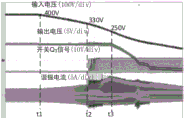
Fig. 27-29 show the results of the prototype at a load current of 25A from normal operation to hold operation. Input voltage from t 1400V at time down to t3At 250V. At time t1To t2During this time, the prototype provided a nominal output voltage (12V). As shown in FIG. 27, when the input voltage drops below 330V, the additional switch at time t2To t3During which the operation is started. The output voltage is maintained at 12V during the hold operation. Fig. 28 shows a waveform (normal operation) when the input voltage is 400V, and fig. 29 showsA waveform when the input voltage is 250V (hold operation) is shown. When the input voltage is 400V, the peak value of the resonant current is at time t1Is 3A, and when the input voltage is 250V, the peak value of the resonance current is at time t3It was 7.5A.
Fig. 30-32 show the results of the prototype at a load current of 15A from normal operation to hold operation. Input voltage from t 1400V at time down to t3At 250V. At time t1To t2During this time, the prototype provided a nominal output voltage (12V). As shown in FIG. 30, when the input voltage drops below 310V, the additional switch at time t2To t3During which the operation is started. The output voltage is maintained at 12V during the hold operation. Fig. 31 shows a waveform when the input voltage is 400V (normal operation), and fig. 29 shows a waveform when the input voltage is 220V (hold operation). When the input voltage is 400V, the peak value of the resonant current is at time t1Is 1.8A, and when the input voltage is 220V, the peak value of the resonance current is at time t3Is 5A.
It should be understood that the foregoing description is only illustrative of the invention. Various alternatives and modifications can be devised by those skilled in the art without departing from the invention. Accordingly, the present invention is intended to embrace all such alternatives, modifications and variances which fall within the scope of the appended claims.
Claims (20)
Applications Claiming Priority (3)
| Application Number | Priority Date | Filing Date | Title |
|---|---|---|---|
| US201562220465P | 2015-09-18 | 2015-09-18 | |
| US62/220,465 | 2015-09-18 | ||
| PCT/US2016/052278 WO2017049179A1 (en) | 2015-09-18 | 2016-09-16 | Converters with hold-up operation |
Publications (2)
| Publication Number | Publication Date |
|---|---|
| CN108028605A CN108028605A (en) | 2018-05-11 |
| CN108028605B true CN108028605B (en) | 2020-05-12 |
Family
ID=58289697
Family Applications (1)
| Application Number | Title | Priority Date | Filing Date |
|---|---|---|---|
| CN201680053678.3A Active CN108028605B (en) | 2015-09-18 | 2016-09-16 | Converter with hold-up operation |
Country Status (3)
| Country | Link |
|---|---|
| US (1) | US10637363B2 (en) |
| CN (1) | CN108028605B (en) |
| WO (1) | WO2017049179A1 (en) |
Families Citing this family (30)
| Publication number | Priority date | Publication date | Assignee | Title |
|---|---|---|---|---|
| US11063520B2 (en) | 2016-12-16 | 2021-07-13 | Murata Manufacturing Co., Ltd. | Simplified hybrid PWM/PFM control method for SLLC converter |
| KR102406659B1 (en) * | 2017-03-07 | 2022-06-08 | 현대자동차주식회사 | A vehicle and a charger for the vehicle |
| US10256744B2 (en) * | 2017-09-12 | 2019-04-09 | Infineon Technologies Austria Ag | Controller device with adaptive synchronous rectification |
| IL255948A (en) * | 2017-11-27 | 2018-01-31 | Abramovici Tal | Constant frequency dc/dc power converter |
| US10944329B2 (en) * | 2018-01-15 | 2021-03-09 | Queen's University At Kingston | Power converter topologies and control methods for wide input and output voltage ranges |
| US11394307B2 (en) * | 2018-01-29 | 2022-07-19 | Queen's University At Kingston | Resonant power converters and control methods for wide input and output voltage ranges |
| CN108306513B (en) * | 2018-02-27 | 2020-08-25 | 成都芯源系统有限公司 | Turn-off control circuit of synchronous rectifier tube and synchronous rectifier control circuit |
| KR102537368B1 (en) * | 2018-03-16 | 2023-05-25 | 현대자동차주식회사 | Power receiving device having bridgeless rectifier in an electric car wireless power transmission system |
| CN108923658B (en) * | 2018-07-09 | 2020-06-09 | 国网冀北电力有限公司张家口供电公司 | LLC resonant converter |
| CN108832818B (en) * | 2018-07-19 | 2020-02-14 | 山东大学 | Resonant type isolation DC-DC converter with wide voltage gain range and modulation method |
| WO2020055669A1 (en) * | 2018-09-12 | 2020-03-19 | Murata Manufacturing Co., Ltd. | Dynamic transient control in resonant converters |
| US10826404B2 (en) * | 2019-03-13 | 2020-11-03 | Infineon Technologies Austria Ag | Bias control in a voltage converter |
| TWI711259B (en) * | 2019-05-30 | 2020-11-21 | 亞源科技股份有限公司 | Resonant converter |
| CN110149055B (en) * | 2019-07-05 | 2023-02-07 | 亚瑞源科技(深圳)有限公司 | Resonance converter |
| ES2913635T3 (en) * | 2019-09-20 | 2022-06-03 | Hitachi Energy Switzerland Ag | Dual active bridge converter cell with split power transfer inductor for optimized current balancing in the medium frequency transformer (MFT) |
| CN111049369B (en) * | 2019-12-25 | 2021-03-16 | 湖北工业大学 | Hybrid control method for resonant converter in distributed power system |
| TWI740619B (en) * | 2020-08-21 | 2021-09-21 | 國立臺灣科技大學 | Control circuit and control method for power converter |
| CN112366949A (en) * | 2020-11-02 | 2021-02-12 | 杭州瑞旗电子科技有限公司 | High-gain LLC resonant converter |
| CN112366966B (en) * | 2020-11-18 | 2024-07-05 | 万明武 | Single-switch half-bridge electric energy converter |
| CN115118174A (en) * | 2021-03-09 | 2022-09-27 | 华为数字能源技术有限公司 | Asymmetric half-bridge flyback converter and power supply system |
| WO2022201448A1 (en) * | 2021-03-25 | 2022-09-29 | Tdk株式会社 | Switching power supply device and power supply system |
| CN115378266B (en) * | 2021-05-19 | 2026-03-17 | 台达电子企业管理(上海)有限公司 | Converters and their control methods applicable to a wide range of output voltages |
| WO2023065230A1 (en) * | 2021-10-21 | 2023-04-27 | Aes Global Holdings Pte Ltd. | Hold-up time circuit for llc converter |
| CN114142733B (en) * | 2021-11-15 | 2023-10-27 | 矽力杰半导体技术(杭州)有限公司 | Switching power supply circuit |
| US11901828B2 (en) * | 2022-02-16 | 2024-02-13 | Zhejiang University | Bidirectional CLLC resonant circuit with coupled inductor |
| US11705815B1 (en) * | 2022-02-22 | 2023-07-18 | Aes Global Holdings Pte Ltd. | Holdup time extension for LLC circuit |
| CN117081400A (en) * | 2022-05-10 | 2023-11-17 | 台达电子工业股份有限公司 | Hybrid power conversion circuit |
| WO2023243321A1 (en) * | 2022-06-17 | 2023-12-21 | パナソニックIpマネジメント株式会社 | Converter device |
| CN116418238B (en) * | 2023-06-08 | 2023-08-15 | 西南交通大学 | Three-switch half-bridge wide-range LLC resonant converter and use method thereof |
| CN118282218B (en) * | 2024-06-03 | 2024-08-27 | 深圳市能效电气技术有限公司 | Control method of isolated DC resonant converter based on CLASS E |
Citations (5)
| Publication number | Priority date | Publication date | Assignee | Title |
|---|---|---|---|---|
| CN1747308A (en) * | 2005-09-26 | 2006-03-15 | 艾默生网络能源有限公司 | Control of resonant circuit output characteristics and resonant circuit |
| CN101093961A (en) * | 2006-06-22 | 2007-12-26 | 台达电子工业股份有限公司 | Resonant converter and its light-load and no-load regulation method |
| CN101951152A (en) * | 2009-06-24 | 2011-01-19 | 意法半导体股份有限公司 | Heterogeneous resonance converter and control its method |
| KR101492964B1 (en) * | 2013-10-15 | 2015-02-24 | 전주대학교 산학협력단 | SLLC Resonant Converter for Bidirectional Power Conversion using auxiliary switches and inductor |
| CN204304823U (en) * | 2015-01-23 | 2015-04-29 | 哈尔滨理工大学 | Based on the synchronous rectification soft switch transducer that phase-shifting full-bridge controls |
Family Cites Families (10)
| Publication number | Priority date | Publication date | Assignee | Title |
|---|---|---|---|---|
| US7012380B2 (en) * | 2004-06-24 | 2006-03-14 | Dell Products L.P. | Information handling system with dual mode inverter |
| TWI313102B (en) | 2005-02-21 | 2009-08-01 | Delta Electronics Inc | Llc series resonant converter and the driving method of the synchronous rectifier power switches thereof |
| US8014173B2 (en) * | 2008-10-16 | 2011-09-06 | Fsp Technology Inc. | Resonant converter for synchronous rectification control |
| EP2381570B1 (en) | 2010-04-20 | 2013-01-02 | DET International Holding Limited | Resonant capacitor clamping circuit in resonant converter |
| JP5589701B2 (en) * | 2010-09-15 | 2014-09-17 | 富士電機株式会社 | Power factor improving current resonance converter |
| KR20130026714A (en) * | 2011-09-06 | 2013-03-14 | 주식회사 동아일렉콤 | Synchronize rectifier driver circuit for llc resonant half bridge converter |
| WO2013106692A1 (en) | 2012-01-13 | 2013-07-18 | Power-One, Inc. | Resonant converter with auxiliary resonant components and holdup time control circuitry |
| US20130279205A1 (en) | 2012-04-11 | 2013-10-24 | Power-One, Inc. | Hold-up time enhancement circuit for llc resonant converter |
| CN103326581B (en) | 2013-06-24 | 2016-04-13 | 成都芯源系统有限公司 | LLC resonant converter, control circuit and driving method |
| US9548668B2 (en) * | 2014-03-14 | 2017-01-17 | Futurewei Technologies, Inc. | Hybrid power converter and method |
-
2016
- 2016-09-16 US US15/757,548 patent/US10637363B2/en active Active
- 2016-09-16 WO PCT/US2016/052278 patent/WO2017049179A1/en not_active Ceased
- 2016-09-16 CN CN201680053678.3A patent/CN108028605B/en active Active
Patent Citations (5)
| Publication number | Priority date | Publication date | Assignee | Title |
|---|---|---|---|---|
| CN1747308A (en) * | 2005-09-26 | 2006-03-15 | 艾默生网络能源有限公司 | Control of resonant circuit output characteristics and resonant circuit |
| CN101093961A (en) * | 2006-06-22 | 2007-12-26 | 台达电子工业股份有限公司 | Resonant converter and its light-load and no-load regulation method |
| CN101951152A (en) * | 2009-06-24 | 2011-01-19 | 意法半导体股份有限公司 | Heterogeneous resonance converter and control its method |
| KR101492964B1 (en) * | 2013-10-15 | 2015-02-24 | 전주대학교 산학협력단 | SLLC Resonant Converter for Bidirectional Power Conversion using auxiliary switches and inductor |
| CN204304823U (en) * | 2015-01-23 | 2015-04-29 | 哈尔滨理工大学 | Based on the synchronous rectification soft switch transducer that phase-shifting full-bridge controls |
Non-Patent Citations (1)
| Title |
|---|
| A Half-Bridge LLC Resonant Converter Adopting Boost PWM Control Scheme for Hold-Up State Operation;In-Ho Cho,et.al;《IEEE Transactions on Power Electronics》;20130412;第29卷(第2期);第841-850页 * |
Also Published As
| Publication number | Publication date |
|---|---|
| CN108028605A (en) | 2018-05-11 |
| US20180248489A1 (en) | 2018-08-30 |
| WO2017049179A1 (en) | 2017-03-23 |
| US10637363B2 (en) | 2020-04-28 |
Similar Documents
| Publication | Publication Date | Title |
|---|---|---|
| CN108028605B (en) | Converter with hold-up operation | |
| TWI750780B (en) | Isolated dc/dc converters for wide output voltage range and control methods thereof | |
| US9660536B2 (en) | Switching power supply device performs power transmission by using resonance phenomenon | |
| US9263960B2 (en) | Power converters for wide input or output voltage range and control methods thereof | |
| US7023186B2 (en) | Two stage boost converter topology | |
| CN111181408A (en) | Resonant converter based on hybrid rectification structure and control method | |
| WO2021042773A1 (en) | Llc resonant converter and control method | |
| KR102009351B1 (en) | High Efficiency LLC Resonant Converter with Balanced Secondary Currents using the Two Transformer Structure | |
| WO2020248472A1 (en) | Asymmetric half-bridge converter and control method therefor | |
| US20120044722A1 (en) | Isolated switching converter | |
| CN111669055B (en) | Voltage conversion circuit and control method thereof | |
| US8014177B2 (en) | Switching power supply with pulse frequency modulation control | |
| CN111049369A (en) | A hybrid control method for resonant converters in distributed power systems | |
| US11601060B2 (en) | Switch-mode power supplies including three-level LLC circuits for low line and high line operation | |
| WO2019206067A1 (en) | Switched-mode power supply circuit | |
| US11146176B2 (en) | Switch-mode power supplies including three-level LLC circuits | |
| US8711588B1 (en) | Power supply device | |
| CN114930703B (en) | DC power converter | |
| US8665610B2 (en) | Modified zero voltage transition (ZVT) full bridge converter and photovoltaic (PV) array using the same | |
| US20140133190A1 (en) | Isolated switch-mode dc/dc converter with sine wave transformer voltages | |
| CN117378136A (en) | Converters and power adapters | |
| US7388761B1 (en) | High efficiency parallel post regulator for wide range input DC/DC converter | |
| JP7233633B1 (en) | switching power supply circuit | |
| JP4093116B2 (en) | Power factor converter | |
| KR102030918B1 (en) | High Efficiency EV Charger with Small Ripple Current |
Legal Events
| Date | Code | Title | Description |
|---|---|---|---|
| PB01 | Publication | ||
| PB01 | Publication | ||
| SE01 | Entry into force of request for substantive examination | ||
| SE01 | Entry into force of request for substantive examination | ||
| GR01 | Patent grant | ||
| GR01 | Patent grant |