CN107968471B - LCLC resonant circuit, wide-range constant power output DC charger and control method - Google Patents

LCLC resonant circuit, wide-range constant power output DC charger and control method Download PDF

Info

Publication number
CN107968471B
CN107968471B CN201711158056.XA CN201711158056A CN107968471B CN 107968471 B CN107968471 B CN 107968471B CN 201711158056 A CN201711158056 A CN 201711158056A CN 107968471 B CN107968471 B CN 107968471B
Authority
CN
China
Prior art keywords
output
charger
mode
resonant circuit
bridge mode
Prior art date
Legal status (The legal status is an assumption and is not a legal conclusion. Google has not performed a legal analysis and makes no representation as to the accuracy of the status listed.)
Active
Application number
CN201711158056.XA
Other languages
Chinese (zh)
Other versions
CN107968471A (en
Inventor
杨勇
杨军虎
丁玉华
刘爱忠
黄厚诚
孙永亮
于波峰
唐亮
冯立玮
马桂荣
Current Assignee (The listed assignees may be inaccurate. Google has not performed a legal analysis and makes no representation or warranty as to the accuracy of the list.)
Shandong Luruan Digital Technology Co ltd Smart Energy Branch
Original Assignee
State Grid Intelligent Technology Co Ltd
Priority date (The priority date is an assumption and is not a legal conclusion. Google has not performed a legal analysis and makes no representation as to the accuracy of the date listed.)
Filing date
Publication date
Application filed by State Grid Intelligent Technology Co Ltd filed Critical State Grid Intelligent Technology Co Ltd
Priority to CN201711158056.XA priority Critical patent/CN107968471B/en
Publication of CN107968471A publication Critical patent/CN107968471A/en
Application granted granted Critical
Publication of CN107968471B publication Critical patent/CN107968471B/en
Active legal-status Critical Current
Anticipated expiration legal-status Critical

Links

Images

Classifications

    • H02J7/045
    • BPERFORMING OPERATIONS; TRANSPORTING
    • B60VEHICLES IN GENERAL
    • B60LPROPULSION OF ELECTRICALLY-PROPELLED VEHICLES; SUPPLYING ELECTRIC POWER FOR AUXILIARY EQUIPMENT OF ELECTRICALLY-PROPELLED VEHICLES; ELECTRODYNAMIC BRAKE SYSTEMS FOR VEHICLES IN GENERAL; MAGNETIC SUSPENSION OR LEVITATION FOR VEHICLES; MONITORING OPERATING VARIABLES OF ELECTRICALLY-PROPELLED VEHICLES; ELECTRIC SAFETY DEVICES FOR ELECTRICALLY-PROPELLED VEHICLES
    • B60L53/00Methods of charging batteries, specially adapted for electric vehicles; Charging stations or on-board charging equipment therefor; Exchange of energy storage elements in electric vehicles
    • B60L53/20Methods of charging batteries, specially adapted for electric vehicles; Charging stations or on-board charging equipment therefor; Exchange of energy storage elements in electric vehicles characterised by converters located in the vehicle
    • HELECTRICITY
    • H02GENERATION; CONVERSION OR DISTRIBUTION OF ELECTRIC POWER
    • H02MAPPARATUS FOR CONVERSION BETWEEN AC AND AC, BETWEEN AC AND DC, OR BETWEEN DC AND DC, AND FOR USE WITH MAINS OR SIMILAR POWER SUPPLY SYSTEMS; CONVERSION OF DC OR AC INPUT POWER INTO SURGE OUTPUT POWER; CONTROL OR REGULATION THEREOF
    • H02M7/00Conversion of AC power input into DC power output; Conversion of DC power input into AC power output
    • H02M7/42Conversion of DC power input into AC power output without possibility of reversal
    • H02M7/44Conversion of DC power input into AC power output without possibility of reversal by static converters
    • H02M7/48Conversion of DC power input into AC power output without possibility of reversal by static converters using discharge tubes with control electrode or semiconductor devices with control electrode
    • HELECTRICITY
    • H02GENERATION; CONVERSION OR DISTRIBUTION OF ELECTRIC POWER
    • H02MAPPARATUS FOR CONVERSION BETWEEN AC AND AC, BETWEEN AC AND DC, OR BETWEEN DC AND DC, AND FOR USE WITH MAINS OR SIMILAR POWER SUPPLY SYSTEMS; CONVERSION OF DC OR AC INPUT POWER INTO SURGE OUTPUT POWER; CONTROL OR REGULATION THEREOF
    • H02M7/00Conversion of AC power input into DC power output; Conversion of DC power input into AC power output
    • H02M7/42Conversion of DC power input into AC power output without possibility of reversal
    • H02M7/44Conversion of DC power input into AC power output without possibility of reversal by static converters
    • H02M7/48Conversion of DC power input into AC power output without possibility of reversal by static converters using discharge tubes with control electrode or semiconductor devices with control electrode
    • H02M7/4815Resonant converters
    • YGENERAL TAGGING OF NEW TECHNOLOGICAL DEVELOPMENTS; GENERAL TAGGING OF CROSS-SECTIONAL TECHNOLOGIES SPANNING OVER SEVERAL SECTIONS OF THE IPC; TECHNICAL SUBJECTS COVERED BY FORMER USPC CROSS-REFERENCE ART COLLECTIONS [XRACs] AND DIGESTS
    • Y02TECHNOLOGIES OR APPLICATIONS FOR MITIGATION OR ADAPTATION AGAINST CLIMATE CHANGE
    • Y02TCLIMATE CHANGE MITIGATION TECHNOLOGIES RELATED TO TRANSPORTATION
    • Y02T10/00Road transport of goods or passengers
    • Y02T10/60Other road transportation technologies with climate change mitigation effect
    • Y02T10/70Energy storage systems for electromobility, e.g. batteries
    • YGENERAL TAGGING OF NEW TECHNOLOGICAL DEVELOPMENTS; GENERAL TAGGING OF CROSS-SECTIONAL TECHNOLOGIES SPANNING OVER SEVERAL SECTIONS OF THE IPC; TECHNICAL SUBJECTS COVERED BY FORMER USPC CROSS-REFERENCE ART COLLECTIONS [XRACs] AND DIGESTS
    • Y02TECHNOLOGIES OR APPLICATIONS FOR MITIGATION OR ADAPTATION AGAINST CLIMATE CHANGE
    • Y02TCLIMATE CHANGE MITIGATION TECHNOLOGIES RELATED TO TRANSPORTATION
    • Y02T10/00Road transport of goods or passengers
    • Y02T10/60Other road transportation technologies with climate change mitigation effect
    • Y02T10/7072Electromobility specific charging systems or methods for batteries, ultracapacitors, supercapacitors or double-layer capacitors
    • YGENERAL TAGGING OF NEW TECHNOLOGICAL DEVELOPMENTS; GENERAL TAGGING OF CROSS-SECTIONAL TECHNOLOGIES SPANNING OVER SEVERAL SECTIONS OF THE IPC; TECHNICAL SUBJECTS COVERED BY FORMER USPC CROSS-REFERENCE ART COLLECTIONS [XRACs] AND DIGESTS
    • Y02TECHNOLOGIES OR APPLICATIONS FOR MITIGATION OR ADAPTATION AGAINST CLIMATE CHANGE
    • Y02TCLIMATE CHANGE MITIGATION TECHNOLOGIES RELATED TO TRANSPORTATION
    • Y02T10/00Road transport of goods or passengers
    • Y02T10/80Technologies aiming to reduce greenhouse gasses emissions common to all road transportation technologies
    • Y02T10/92Energy efficient charging or discharging systems for batteries, ultracapacitors, supercapacitors or double-layer capacitors specially adapted for vehicles
    • YGENERAL TAGGING OF NEW TECHNOLOGICAL DEVELOPMENTS; GENERAL TAGGING OF CROSS-SECTIONAL TECHNOLOGIES SPANNING OVER SEVERAL SECTIONS OF THE IPC; TECHNICAL SUBJECTS COVERED BY FORMER USPC CROSS-REFERENCE ART COLLECTIONS [XRACs] AND DIGESTS
    • Y02TECHNOLOGIES OR APPLICATIONS FOR MITIGATION OR ADAPTATION AGAINST CLIMATE CHANGE
    • Y02TCLIMATE CHANGE MITIGATION TECHNOLOGIES RELATED TO TRANSPORTATION
    • Y02T90/00Enabling technologies or technologies with a potential or indirect contribution to GHG emissions mitigation
    • Y02T90/10Technologies relating to charging of electric vehicles
    • Y02T90/14Plug-in electric vehicles

Landscapes

  • Engineering & Computer Science (AREA)
  • Power Engineering (AREA)
  • Transportation (AREA)
  • Mechanical Engineering (AREA)
  • Charge And Discharge Circuits For Batteries Or The Like (AREA)
  • Dc-Dc Converters (AREA)

Abstract

本发明公开了一种LCLC谐振电路、宽范围恒功率输出直流充电机及控制方法,包括:串联谐振电感、串联谐振电容和并联谐振电感组成的串并联谐振网络;在所述并联谐振电感的支路上串入电容。本发明有益效果:本发明设计的充电机具有更宽的电压输出范围,输出范围为750‑200V;同时本发明设计的充电机具有更高的整体工作效率,尤其充电机低压输出时效率提升明显。
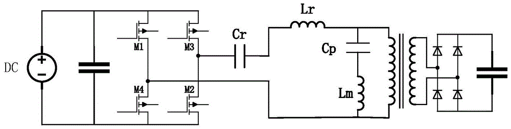
Figure 201711158056

The invention discloses an LCLC resonant circuit, a wide-range constant power output DC charger and a control method, comprising: a series-parallel resonant network composed of a series resonant inductor, a series resonant capacitor and a parallel resonant inductor; A capacitor is connected in series on the road. Beneficial effects of the present invention: the charger designed by the present invention has a wider voltage output range, and the output range is 750-200V; at the same time, the charger designed by the present invention has higher overall working efficiency, especially when the charger is low-voltage output, the efficiency is significantly improved .

Figure 201711158056

Description

LCLC resonance circuit, wide-range constant-power output direct-current charger and control method
Technical Field
The invention relates to the field of direct-current charging of new energy electric vehicles, in particular to an LCLC resonance circuit, a wide-range constant-power output direct-current charger based on an LCLC resonance technology and a control method of the charger.
Background
LLC resonant circuits are recently attracting attention from industry research, and theoretical research thereof has been well developed. It has some obvious advantages over traditional hard switching techniques: the ZVS switching-on of the MOS tube can be realized within a variable frequency range, so that the switching loss of a circuit is reduced, and the efficiency of the converter is improved; when the switching frequency is lower than or equal to the resonant frequency, the rectifier diode is naturally turned off, and the turn-off loss and the voltage spike of the rectifier part are eliminated; the current waveform is sine wave, and the conduction and radiation interference is small; the circuit has high switching frequency, reduces the size of a power device and a converter, and improves the power density of the module. Based on the advantages, the LLC resonant circuit is widely applied to the direct-current charger of the electric automobile.
LLC resonant circuits also have their inherent disadvantages: because the output/input gain curve is slow, the switching frequency of the power MOS tube is increased when the low-voltage is output, the switching loss of the power MOS tube is increased, and the efficiency of the LLC converter is reduced. The LLC resonant circuit switching frequency must therefore be limited or the converter thermal problem is severe. Therefore, to maintain high output efficiency, LLC resonant circuits are not suitable for wide-range output environments.
With the continuous input and support of the country to new energy automobiles, domestic new energy automobiles are greatly developed, various new energy automobile models are continuously released, but due to the imperfect relevant standards, the charging voltage of lithium batteries used by domestic new energy automobiles is refuted, and the range is from 200V to 750V. The charger designed based on the traditional LLC resonant circuit is difficult to realize the constant power output in such a wide range.
The existing direct current charger based on the LLC resonance technology is generally divided into two types according to the output voltage:
1. the output voltage is 500-200V.
2. The output voltage is 750-300V.
Any one of the above types cannot meet the requirements of all automobiles for charging, so that the complexity and cost of automobile charging facility construction are increased in a phase-changing manner, and the experience of customers during charging is influenced.
Disclosure of Invention
The invention aims to solve the problems and provides an LCLC resonance circuit, a wide-range constant-power-output direct-current charger based on an LCLC resonance technology and a control method thereof.
In order to achieve the purpose, the invention adopts the following specific scheme:
the invention discloses an LCLC resonance circuit, comprising: a series-parallel resonant network consisting of a series resonant inductor, a series resonant capacitor and a parallel resonant inductor; and a capacitor is connected in series on a branch circuit of the parallel resonance inductor.
The invention also discloses a wide-range constant-power output direct-current charger, which comprises: the device comprises an input module, a rectifying module and an output module; connecting the LCLC resonant circuit of claim 1 between the rectification module and the output module;
the LCLC resonant circuit is connected with a DSP controller, and the DSP controller controls the LCLC resonant circuit to be switched between a full-bridge mode and a half-bridge mode.
Further, the working areas of the full-bridge mode and the half-bridge mode are divided according to the output voltage of the charger: when the output voltage is greater than A2, the LCLC resonance circuit is controlled to work in a full-bridge mode, and when the output voltage is less than A1, the LCLC resonance circuit works in a half-bridge mode;
a1 and A2 are set voltage values.
Further, the DSP controller controls the LCLC resonant circuit to adopt one of PFM, fixed frequency and width modulation, or burst mode, or any two or three of them in combination.
Furthermore, a PFM control mode is adopted when the DSP controller outputs B2-B3 through a digital PI; when the digital PI output of the DSP controller is B1-B2, a control mode of fixed frequency and width modulation is adopted; when the digital PI output of the DSP controller is less than B1, a burst mode control mode is adopted;
among them, B1, B2, and B3 are all set voltage values.
The invention further discloses a control method of the wide-range constant-power output direct-current charger, which comprises the following steps:
dividing working areas of a full-bridge mode and a half-bridge mode according to the output voltage of a charger, and controlling an LCLC resonant circuit to switch between the full-bridge mode and the half-bridge mode by taking the current output voltage of the charger as a switching basis of the full-bridge mode and the half-bridge mode;
and controlling the LCLC resonant circuit by adopting a PFM (pulse frequency modulation), fixed frequency width modulation or Burst Mode control Mode, or controlling the LCLC resonant circuit by adopting a control Mode combining any two or three of the three control modes.
Further, when the output voltage is greater than A2, the LCLC resonant circuit is controlled to operate in a full-bridge mode, and when the output voltage is less than A1, the LLC resonant circuit is controlled to operate in a half-bridge mode;
a1 and A2 are set voltage values.
Further, a specific method for controlling the LCLC resonant circuit to switch between the full-bridge mode and the half-bridge mode is as follows:
when the output voltage of the charger is greater than A2, the LCLC resonant circuit works in a full-bridge mode; the DSP controller firstly outputs a driving signal according to a full-bridge mode, and then adjusts a front-stage PFC circuit to output a corresponding bus voltage;
when the output voltage of the charger is between A1 and A2, full-bridge and half-bridge switching is not needed; the DSP controller judges the current mode of the LCLC resonance circuit, and if the LCLC resonance circuit is in a full-bridge mode, the DSP controller regulates the lowest bus voltage output by the front-stage PFC circuit; if the front-stage PFC circuit is in a half-bridge mode, the DSP controller adjusts the highest bus voltage output by the front-stage PFC circuit;
when the output voltage of the charger is less than A1, the LCLC resonant circuit works in a half-bridge mode; the DSP controller firstly adjusts the highest bus voltage output by the front-stage PFC circuit and then outputs a driving signal according to a half-bridge mode;
a1 and A2 are set voltage values.
Further, when the digital PI output of the DSP controller is B2-B3, a PFM control mode is adopted;
when the digital PI output of the DSP controller is B1-B2, a control mode of fixed frequency and width modulation is adopted; at the moment, the switching frequency of the DSP controller is kept at a set frequency value, but the duty ratio of the driving signal is reduced;
when the digital PI output of the DSP controller is less than B1, a Burst Mode control Mode is adopted; at the moment, the DSP controller intermittently generates a driving signal with set frequency and set duty ratio;
among them, B1, B2, and B3 are all set voltage values.
The invention has the beneficial effects that:
compared with the conventional charger realized based on the conventional LLC resonant circuit, the charger designed by the invention has a wider voltage output range, wherein the output range is 750-200V; meanwhile, the charger designed by the invention has higher overall working efficiency, and the efficiency is obviously improved particularly when the charger outputs low voltage.
Drawings
FIG. 1 is a block diagram of a wide-range constant-power output charger based on LCLC resonance technology;
FIG. 2 is a conventional LLC full bridge resonant circuit;
FIG. 3 is a modified LCLC series resonant circuit;
FIG. 4 is a conventional LLC half-bridge resonant circuit;
FIG. 5 is a diagram of the division of full-bridge and half-bridge working areas of an LCLC resonance circuit according to the output voltage of a charger;
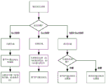
FIG. 6 is a process of switching full-bridge and half-bridge of LCLC resonant circuit controlled by the charger DSP chip;
FIG. 7 is a schematic diagram of a PFM + fixed-frequency-modulation width + Burst Mode control strategy when the LCLC is in a light load or no load state;
FIG. 8 is a schematic diagram of the driving waveforms of the PFM + fixed-frequency-width-modulation + Burst Mode MOS transistor under light load or no load of the LCLC;
FIG. 9 is a gain curve of an LCLC tank circuit for the same Q and different K values;
FIG. 10 shows typical driving waveforms of a power MOS transistor in full-bridge mode;
fig. 11 shows typical driving waveforms of a power MOS transistor in a half-bridge mode.
The specific implementation mode is as follows:
the invention is described in detail below with reference to the accompanying drawings:
compared with the existing direct-current charger realized based on the traditional LLC resonance technology, the direct-current charger provided by the invention mainly improves the LLC resonance circuit of the charger and the control mode of the LLC resonance circuit, thereby widening the voltage output and constant power range of the LLC resonance circuit and improving the integral operation efficiency of the LLC resonance circuit. The details will be described below.
In one aspect, the present invention discloses an LCLC resonant circuit, including: a series-parallel resonant network consisting of a series resonant inductor, a series resonant capacitor and a parallel resonant inductor; and a capacitor is connected in series on a branch circuit of the parallel resonance inductor. The full bridge LLC series resonant circuit is illustrated.
Fig. 2 shows a conventional LLC full-bridge resonant circuit. Fig. 3 is a modified LCLC full bridge resonant circuit.
The improved LCLC resonance circuit has a transformer excitation inductance Lm branch in series connected with a capacitor Cp in the original LLC resonance circuit. The addition of Cp makes the K value of LLC converter no longer fixed, its equivalent K value varies with frequency variation, the lower the frequency, the smaller the equivalent K value. Wherein, K is Lm _ eq/Lr; the LLC resonant circuit Lm _ eq is equal to Lm; the LCLC resonance circuit Lm _ eq is equivalent inductance after Lm and Cp are connected in series.
As can be seen from the graph in fig. 9, when fs (switching frequency) < fr (resonant frequency), the smaller the K value, the steeper the LLC gain curve, and the higher the LCLC output voltage at the same switching frequency, i.e., the LCLC resonant circuit is more suitable for realizing a wide range of output than the LLC resonant circuit.
On the other hand, the invention discloses a direct current charger with wide-range constant power output, as shown in fig. 1, comprising: the device comprises a three-phase alternating current input part, an input side filter, a three-phase Vienna rectification circuit (AC-DC), an LCLC series resonance circuit (DC-DC) improved by the invention, an output filter, a direct current output and a DSP controller.
The three-phase alternating current enters a three-phase Vienna rectifying circuit after being filtered by an input filter, the three-phase Vienna rectifying circuit rectifies input and corrects power factors to obtain a high-voltage direct current bus, the high-voltage direct current bus carries out DC-DC isolation conversion through an LCLC series resonant circuit to output adjustable direct current voltage, and the direct current voltage can charge an automobile lithium battery after being output and filtered. The DSP controller controls the charger to stably output the required direct current charging voltage, and monitors and protects the charger.
In a third aspect, the present invention improves the manner in which LCLC resonant circuits are controlled.
(1) Dividing working areas of a full-bridge mode and a half-bridge mode according to the output voltage of a charger, and controlling the LCLC resonant circuit to switch between the full-bridge mode and the half-bridge mode;
the working areas of the full-bridge mode and the half-bridge mode are divided according to the output voltage of the charger, as shown in fig. 5, when the output voltage is greater than 330V, the LCLC resonant circuit is controlled to work in the full-bridge mode, and when the output voltage is less than 325V, the LCLC resonant circuit works in the half-bridge mode.
Fig. 2 is a conventional LLC full-bridge series resonant circuit, and fig. 4 is a conventional LLC half-bridge series resonant circuit.
The half-bridge topology of fig. 4 can be realized by turning off the MOS transistor M1 in fig. 2 and turning on the transistor M4, and the switching between the full bridge and the half bridge is realized by controlling the driving signals of M1 and M4 through the DSP.
After the LCLC full-bridge resonant circuit is switched to the half-bridge resonant circuit, the output gain is reduced to 1/2 under the same switching frequency and load, so that the output range of the low-voltage section of the LCLC resonant circuit can be expanded by using a full-bridge half-bridge switching control mode, and the running efficiency of the low-voltage section of the charger is improved.
In order to prevent the LCLC resonance circuit from entering a capacitive area in the full-bridge and half-bridge switching process and reduce the output voltage fluctuation in the switching process, the charger DSP controls the LCLC resonance circuit to switch the full-bridge and half-bridge according to the flow of the figure 6.
The DSP controller samples the voltage of the output end of the charger in real time, and the current output voltage of the charger is used as the switching basis of a full-bridge mode and a half-bridge mode by the DSP controller.
When the output voltage of the charger is greater than 330V, the LCLC resonant circuit works in a full-bridge mode. First, the DSP controller outputs a driving signal according to a full-bridge mode, as shown in fig. 10, and then the DSP controller adjusts the output of the corresponding bus voltage from the pre-stage PFC circuit.
When the output voltage of the charger is between 325V and 330V, the LCLC resonant circuit can work in any mode of a full bridge and a half bridge at the moment, namely, the full bridge and the half bridge do not need to be switched in the area, the DSP controller judges the current mode of the LCLC resonant circuit, and if the LCLC resonant circuit is in the full bridge mode, the DSP controller adjusts the lowest bus voltage (590V) output by a front-stage PFC circuit; if the front-stage PFC circuit is in a half-bridge mode, the DSP controller regulates the output highest bus voltage (790V) of the front-stage PFC circuit;
when the output voltage of the charger is less than 325V, the LCLC resonant circuit works in a half-bridge mode. Firstly, the DSP controller regulates the output highest bus voltage (790V) of the front-stage PFC circuit. The DSP controller then outputs the drive signal in half-bridge mode as shown in fig. 11.
(2) And the LCLC resonance circuit is controlled by adopting a control Mode combining PFM, fixed frequency modulation width and Burst Mode.
The charger adopts a control Mode combining PFM, fixed frequency and fixed frequency modulation width and Burst Mode. As shown in FIG. 7, when the DSP control chip digital PI outputs 3-10V, the PFM control Mode is adopted, when the PI outputs 1-3V, the control Mode of fixed frequency and width modulation is adopted, the switching frequency is kept at 250K, but the duty ratio of the driving signal is gradually reduced from 50% to 5%, when the PI output is less than 1V, the Burst Mode control Mode is adopted, when the DSP control chip intermittently generates the driving signal with the frequency of 250K and the duty ratio of 5%, and the detailed driving waveform of each Mode MOS tube is shown in FIG. 8.
By the control method, the wide-range constant power output of the charger is realized.
Although the embodiments of the present invention have been described with reference to the accompanying drawings, it is not intended to limit the scope of the present invention, and it should be understood by those skilled in the art that various modifications and variations can be made without inventive efforts by those skilled in the art based on the technical solution of the present invention.

Claims (8)

1.一种LCLC谐振电路,包括:串联谐振电感、串联谐振电容和并联谐振电感组成的串并联谐振网络;其特征在于,在所述并联谐振电感的支路上串入电容;所述电容的加入使变换器的K值不再固定,其等效的K值随频率变化而变化。1. an LCLC resonant circuit, comprising: a series-parallel resonant network composed of a series resonant inductance, a series resonant capacitor and a parallel resonant inductance; it is characterized in that, a capacitor is inserted in series on the branch of the parallel resonant inductance; the addition of the capacitor The K value of the converter is no longer fixed, and its equivalent K value varies with frequency. 2.一种宽范围恒功率输出直流充电机,包括:输入模块、整流模块和输出模块;其特征在于,在所述整流模块和输出模块之间连接权利要求1所述的LCLC谐振电路;2. A wide-range constant power output DC charger, comprising: an input module, a rectifier module and an output module; it is characterized in that the LCLC resonant circuit of claim 1 is connected between the rectifier module and the output module; 所述LCLC谐振电路与DSP控制器连接,所述DSP控制器控制所述LCLC谐振电路在全桥模式和半桥模式之间切换;所述DSP控制器以充电机当前输出电压作为全桥模式和半桥模式切换依据;The LCLC resonant circuit is connected with the DSP controller, and the DSP controller controls the LCLC resonant circuit to switch between the full-bridge mode and the half-bridge mode; the DSP controller takes the current output voltage of the charger as the full-bridge mode and the half-bridge mode. Half-bridge mode switching basis; 所述DSP控制器控制所述LCLC谐振电路采用PFM、定频调宽或者Burst Mode中的一种控制方式,或者采用其中的任两种或者三种相结合的控制方式。The DSP controller controls the LCLC resonant circuit by adopting one of the control modes of PFM, fixed frequency width modulation or Burst Mode, or by adopting any two or a combination of the three control modes. 3.如权利要求2所述的一种宽范围恒功率输出直流充电机,其特征在于,按照充电机输出电压划分全桥模式与半桥模式的工作区域:当输出电压大于A2时,控制所述LCLC谐振电路工作于全桥模式,输出电压小于A1时,LCLC谐振电路工作于半桥模式;3. A wide-range constant power output DC charger as claimed in claim 2, wherein the working area of the full-bridge mode and the half-bridge mode is divided according to the output voltage of the charger: when the output voltage is greater than A2, the control The LCLC resonant circuit works in the full-bridge mode, and when the output voltage is less than A1, the LCLC resonant circuit works in the half-bridge mode; 其中,A1、A2均为设定的电压值。Among them, A1 and A2 are both set voltage values. 4.如权利要求2所述的一种宽范围恒功率输出直流充电机,其特征在于,当DSP控制器数字PI输出B2-B3时采用PFM控制方式;当DSP控制器数字PI输出在B1-B2时采用定频调宽的控制方式;当DSP控制器数字PI输出小于B1时采取Burst Mode控制方式;4. a kind of wide-range constant power output DC charger as claimed in claim 2, it is characterized in that, adopt PFM control mode when DSP controller digital PI output B2-B3; When DSP controller digital PI output is in B1- B2 adopts the control mode of fixed frequency and width modulation; when the digital PI output of the DSP controller is less than B1, the Burst Mode control mode is adopted; 其中,B1、B2、B3均为设定的电压值。Among them, B1, B2, B3 are all set voltage values. 5.一种如权利要求2所述的宽范围恒功率输出直流充电机的控制方法,其特征在于,包括:5. A control method for a wide-range constant power output DC charger as claimed in claim 2, characterized in that, comprising: 按照充电机输出电压划分全桥模式与半桥模式的工作区域,以充电机当前输出电压作为全桥模式和半桥模式切换依据,控制LCLC谐振电路在全桥模式和半桥模式之间切换;According to the output voltage of the charger, the working area of the full-bridge mode and the half-bridge mode is divided, and the current output voltage of the charger is used as the basis for switching between the full-bridge mode and the half-bridge mode, and the LCLC resonant circuit is controlled to switch between the full-bridge mode and the half-bridge mode; 采用PFM、定频调宽或者Burst Mode的控制方式对LCLC谐振电路进行控制,或者采用上述三种控制方式中的任两种或者三种相结合的控制方式对LCLC谐振电路进行控制。The LCLC resonant circuit is controlled by the control methods of PFM, fixed frequency width modulation or Burst Mode, or any two or a combination of the above three control methods is used to control the LCLC resonant circuit. 6.如权利要求5所述的一种宽范围恒功率输出直流充电机的控制方法,其特征在于,6. The control method of a wide-range constant power output DC charger as claimed in claim 5, characterized in that, 当输出电压大于A2时,控制所述LCLC谐振电路工作于全桥模式,输出电压小于A1时,控制所述LCLC谐振电路工作于半桥模式;When the output voltage is greater than A2, the LCLC resonant circuit is controlled to work in the full-bridge mode, and when the output voltage is less than A1, the LCLC resonant circuit is controlled to work in the half-bridge mode; 其中,A1、A2均为设定的电压值。Among them, A1 and A2 are both set voltage values. 7.如权利要求5所述的一种宽范围恒功率输出直流充电机的控制方法,其特征在于,控制LCLC谐振电路在全桥模式和半桥模式之间切换的具体方法为:7. the control method of a kind of wide-range constant power output DC charger as claimed in claim 5 is characterized in that, the concrete method that controls LCLC resonant circuit to switch between full-bridge mode and half-bridge mode is: 当充电机输出电压大于A2时,LCLC谐振电路工作在全桥模式;DSP控制器首先按照全桥模式输出驱动信号,然后调节前级PFC电路输出相应的母线电压;When the output voltage of the charger is greater than A2, the LCLC resonant circuit works in the full-bridge mode; the DSP controller first outputs the driving signal according to the full-bridge mode, and then adjusts the front-stage PFC circuit to output the corresponding bus voltage; 当充电机输出电压在A1与A2之间时,无需进行全桥与半桥切换;DSP控制器判断LCLC谐振电路当前所处模式,如处于全桥模式,DSP控制器调节前级PFC电路输出最低母线电压;如处于半桥模式,DSP控制器调节前级PFC电路输出最高母线电压;When the output voltage of the charger is between A1 and A2, there is no need to switch between the full-bridge and the half-bridge; the DSP controller determines the current mode of the LCLC resonant circuit. If it is in the full-bridge mode, the DSP controller adjusts the output of the pre-stage PFC circuit to the lowest Bus voltage; if in half-bridge mode, the DSP controller adjusts the front-stage PFC circuit to output the highest bus voltage; 当充电机输出电压小于A1时,LCLC谐振电路工作在半桥模式;DSP控制器首先调节前级PFC电路输出最高母线电压,然后按照半桥模式输出驱动信号;When the output voltage of the charger is less than A1, the LCLC resonant circuit works in the half-bridge mode; the DSP controller first adjusts the front-stage PFC circuit to output the highest bus voltage, and then outputs the driving signal according to the half-bridge mode; 其中,A1、A2均为设定的电压值。Among them, A1 and A2 are both set voltage values. 8.如权利要求5所述的一种宽范围恒功率输出直流充电机的控制方法,其特征在于,8. The control method of a wide-range constant power output DC charger as claimed in claim 5, characterized in that, 当DSP控制器数字PI输出为B2-B3时,采用PFM控制方式;When the digital PI output of the DSP controller is B2-B3, the PFM control method is adopted; 当DSP控制器数字PI输出为B1-B2时,采用定频调宽的控制方式;此时DSP控制器的开关频率保持在设定频率值,但驱动信号占空比减小;When the digital PI output of the DSP controller is B1-B2, the control method of fixed frequency and width modulation is adopted; at this time, the switching frequency of the DSP controller remains at the set frequency value, but the duty cycle of the driving signal is reduced; 当DSP控制器数字PI输出小于B1时,采取Burst Mode控制方式;此时DSP控制器间歇性的产生频率设定,占空比设定的驱动信号;When the digital PI output of the DSP controller is less than B1, the Burst Mode control method is adopted; at this time, the DSP controller intermittently generates the drive signal with the frequency setting and the duty cycle setting; 其中,B1、B2、B3均为设定的电压值。Among them, B1, B2, B3 are all set voltage values.
CN201711158056.XA 2017-11-20 2017-11-20 LCLC resonant circuit, wide-range constant power output DC charger and control method Active CN107968471B (en)

Priority Applications (1)

Application Number Priority Date Filing Date Title
CN201711158056.XA CN107968471B (en) 2017-11-20 2017-11-20 LCLC resonant circuit, wide-range constant power output DC charger and control method

Applications Claiming Priority (1)

Application Number Priority Date Filing Date Title
CN201711158056.XA CN107968471B (en) 2017-11-20 2017-11-20 LCLC resonant circuit, wide-range constant power output DC charger and control method

Publications (2)

Publication Number Publication Date
CN107968471A CN107968471A (en) 2018-04-27
CN107968471B true CN107968471B (en) 2020-03-24

Family

ID=62001248

Family Applications (1)

Application Number Title Priority Date Filing Date
CN201711158056.XA Active CN107968471B (en) 2017-11-20 2017-11-20 LCLC resonant circuit, wide-range constant power output DC charger and control method

Country Status (1)

Country Link
CN (1) CN107968471B (en)

Families Citing this family (8)

* Cited by examiner, † Cited by third party
Publication number Priority date Publication date Assignee Title
CN110015058B (en) * 2018-07-11 2021-10-08 中兴通讯股份有限公司 A charging pile and charging method
CN111800013A (en) 2019-04-08 2020-10-20 株式会社村田制作所 LLC converter capable of reducing exciting current and providing high gain
CN110941322A (en) * 2019-12-06 2020-03-31 苏州浪潮智能科技有限公司 A method and system for optimizing server power
CN111181407B (en) * 2020-01-19 2022-08-26 天津大学 C-LLCT-LLT type resonance direct current converter
CN111262442A (en) * 2020-01-22 2020-06-09 湖北工业大学 A Resonant Converter Based on ON/OFF Control
CN111224555B (en) * 2020-04-23 2020-08-25 深圳市健网科技有限公司 Wide-range output control method of LLC resonant conversion circuit
CN113346594B (en) * 2021-06-29 2024-02-09 阳光电源股份有限公司 Charging circuit, control method of charging circuit, controller of charging circuit and charging pile
TWI814062B (en) 2021-08-19 2023-09-01 亞源科技股份有限公司 Llc resonant converting apparatus

Citations (5)

* Cited by examiner, † Cited by third party
Publication number Priority date Publication date Assignee Title
CN105024551A (en) * 2014-04-16 2015-11-04 艾默生网络能源有限公司 Resonance circuit, charger and uninterrupted power supply
CN106411139A (en) * 2016-10-20 2017-02-15 华北电力大学 Control method for LLC current converter with wide output range
CN106787765A (en) * 2017-02-06 2017-05-31 山东鲁能智能技术有限公司 The system and method for realizing ultra-wide output voltage range based on LLC topologys
CN107196512A (en) * 2017-06-21 2017-09-22 国电南瑞科技股份有限公司 The wide range output control method of LLC resonant transform circuits
CN107809178A (en) * 2017-11-03 2018-03-16 上海联影医疗科技有限公司 A kind of high pressure generator and its control method

Patent Citations (5)

* Cited by examiner, † Cited by third party
Publication number Priority date Publication date Assignee Title
CN105024551A (en) * 2014-04-16 2015-11-04 艾默生网络能源有限公司 Resonance circuit, charger and uninterrupted power supply
CN106411139A (en) * 2016-10-20 2017-02-15 华北电力大学 Control method for LLC current converter with wide output range
CN106787765A (en) * 2017-02-06 2017-05-31 山东鲁能智能技术有限公司 The system and method for realizing ultra-wide output voltage range based on LLC topologys
CN107196512A (en) * 2017-06-21 2017-09-22 国电南瑞科技股份有限公司 The wide range output control method of LLC resonant transform circuits
CN107809178A (en) * 2017-11-03 2018-03-16 上海联影医疗科技有限公司 A kind of high pressure generator and its control method

Also Published As

Publication number Publication date
CN107968471A (en) 2018-04-27

Similar Documents

Publication Publication Date Title
CN107968471B (en) LCLC resonant circuit, wide-range constant power output DC charger and control method
Oude Aarninkhof et al. A reconfigurable two-stage 11 kW DC–DC resonant converter for EV charging with a 150–1000 V output voltage range
CN109560711B (en) Isolated bidirectional DC-DC converter and modulation method thereof
CN110620517B (en) An aging power supply device with parallel input and series output
CN106208769B (en) Power conversion device
CN205883057U (en) Ware drive power supply is used to microwave based on LCC resonance network
Dusmez et al. A fully integrated three-level isolated single-stage PFC converter
CN108696140A (en) Full-bridge resonance DC-DC converter with wide output voltage range and modulator approach
US9543823B2 (en) Power conversion apparatus having a switching circuit unit that includes a switching device and an auxiliary switching device
CN105141135B (en) The control method of multi-channel parallel full-bridge LLC converters in a kind of cascading power source system
CN103872920A (en) Leakage inductance current slope direct control method of isolation type two-way three-level converter
CN114079384B (en) A variable structure LLC converter with wide output voltage range and method
CN112234835A (en) Variable structure combined LLC resonant converter
CN108880268A (en) The multi-mode control method of the semi-active bridge DC-DC converter of voltage-source type
CN104578806B (en) Cascade bilateral soft switch DC/DC circuit topology
CN107482922A (en) A kind of two-way LLC resonant converter based on switching switch
CN209375466U (en) A Wide Gain LLC Resonant Converter
CN107612340A (en) A low-voltage stress isolation full-bridge converter circuit device
US12246609B2 (en) Charging device and method for operating the charging device
CN106685251A (en) Single-inductor double Buck full-bridge inverter with diode series-parallel structure and its control method
CN105978327A (en) Boost converter and control method therefor
CN205017081U (en) Soft switch charging device of LCC with power factor calibration function
CN103269160B (en) Three-state direct current-direct current converter and control method thereof
CN110492753A (en) A kind of equivalent control method of the two-way full-bridge DC-DC converter with energy storage inductor
WO2026085990A1 (en) Energy conversion apparatus, and vehicle

Legal Events

Date Code Title Description
PB01 Publication
PB01 Publication
SE01 Entry into force of request for substantive examination
CB02 Change of applicant information

Address after: 250101 block B, Yinhe building, 2008 Xinjie street, hi tech Zone, Ji'nan, Shandong.

Applicant after: Shandong Luneng Intelligent Technology Co., Ltd.

Address before: 250101 B block 626, Yinhe building, 2008 Xinjie street, Ji'nan high tech Zone, Shandong.

Applicant before: Shandong Luneng Intelligent Technology Co., Ltd.

CB02 Change of applicant information

Address after: 250101 Electric Power Intelligent Robot Production Project 101 in Jinan City, Shandong Province, South of Feiyue Avenue and East of No. 26 Road (ICT Industrial Park)

Applicant after: National Network Intelligent Technology Co., Ltd.

Address before: 250101 block B, Yinhe building, 2008 Xinjie street, hi tech Zone, Ji'nan, Shandong.

Applicant before: Shandong Luneng Intelligent Technology Co., Ltd.

CB02 Change of applicant information
GR01 Patent grant
GR01 Patent grant
TR01 Transfer of patent right

Effective date of registration: 20201210

Address after: Room 902, 9 / F, block B, Yinhe building, 2008 Xinluo street, hi tech Zone, Jinan City, Shandong Province

Patentee after: Shandong Luneng Software Technology Co.,Ltd. intelligent electrical branch

Address before: 250101 power intelligent robot production project 101 south of Feiyue Avenue and east of No.26 Road (in ICT Industrial Park) in Suncun District of Gaoxin, Jinan City, Shandong Province

Patentee before: National Network Intelligent Technology Co.,Ltd.

CP01 Change in the name or title of a patent holder

Address after: Room 902, 9 / F, block B, Yinhe building, 2008 Xinluo street, hi tech Zone, Jinan City, Shandong Province

Patentee after: Shandong luruan Digital Technology Co.,Ltd. smart energy branch

Address before: Room 902, 9 / F, block B, Yinhe building, 2008 Xinluo street, hi tech Zone, Jinan City, Shandong Province

Patentee before: Shandong Luneng Software Technology Co.,Ltd. intelligent electrical branch