The invention relates to a divisional application of an LED filament, a manufacturing method thereof and an LED bulb lamp applying the filament, wherein the divisional application is filed on 2016, 12 months and 14 days by the Chinese patent office with the application number of 201611155896.6.
Detailed Description
In order to make the aforementioned objects, features and advantages of the present invention comprehensible, embodiments accompanied with figures are described in detail below.
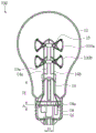
In the manufacturing process of the traditional bulb lamp, in order to avoid oxidation fracture failure caused by combustion of tungsten filaments in air, a glass structure sleeve of a horn core column is designed to be sintered and sealed at an opening of a glass lamp housing, then the inside air of the lamp housing is pumped into nitrogen by a port connection vacuum pump of the horn core column, the combustion oxidation of the tungsten filaments inside the lamp housing is avoided, and finally the port of the horn core column is sintered and sealed. In addition, the water mist dispersed in the air in the lamp shell can be removed at the same time by the replacement of the gas. Further, referring to fig. 1A, fig. 1A shows an LED bulb 1 using an LED filament 11, where the LED bulb 1 includes a lamp housing 12, a plurality of LED filaments 11, an auxiliary support 13 for connecting and supporting the LED filaments 11, a metal stem 14 for exhausting and exchanging gas in the LED bulb 1 and providing a heat conduction function, a heat sink 157 connected to the metal stem 14 and conducting heat from the metal stem 14 to the outside of the LED bulb, a plastic lamp base 157, a lamp head 16, and a driving circuit (not shown) disposed in the lamp head 16. In order to improve the light efficiency performance of the LED bulb lamp 1, the lamp housing 12 must have better transparency and heat conduction effect, therefore, the embodiment adopts a glass lamp housing as a good material, and in addition, a plastic lamp housing with high light transmittance and high heat conduction effect is also selectable, and considering the requirements of part of markets for low color temperature bulb lamps, a material with golden yellow color can be properly doped in the lamp housing, or a layer of golden yellow film is plated on the inner surface of the lamp housing, and a proper trace amount of blue light emitted by part of the LED chips is absorbed, so as to lower the color temperature performance of the LED bulb lamp 1. As mentioned above, the vacuum pump can change the air inside the lamp housing into full nitrogen or mix nitrogen and helium in a proper ratio through the metal stem 14 to improve the thermal conductivity of the gas inside the lamp housing and remove the water mist hidden in the air. In addition, the heat generated by the LED filament 11 is not easily conducted to the outside of the lamp envelope directly without the aid of the metal support, but the heat source radiated from the LED filament 11 is absorbed by the metal stem 14, so that the heat can be rapidly conducted to the heat sink 157 to be discharged to the outside of the lamp envelope. In addition, if the problem of improving the light effect performance is considered, a traditional non-light-absorbing glass core column can be adopted, and a layer of graphene which is light-permeable and has high heat conduction characteristic is plated on the surface of the glass core column, so that the heat dissipation problem can be improved. The heat sink 157 is a hollow cylinder surrounding the open end of the lamp housing 12, and the driving circuit of the LED filament 11 can be placed inside, and the material of the heat sink 157 can be metal, ceramic or high thermal conductivity plastic with good thermal conductivity, and when a metal material (e.g. Al aluminum) is selected as the heat sink 157, the metal material has good thermal conductivity but poor thermal radiation property (e.g. the emissivity of aluminum is only about 0.1), so the surface needs to be coated to enhance the thermal radiation effect, for example, alumina (emissivity is about 0.4) has good thermal radiation effect. The heat sink 157 is preferably provided with a cover plate 1501 on the end surface near the opening of the lamp housing 12, and the surface of the cover plate can be coated with aluminum oxide or white reflective paint, so that the heat conduction area of the heat sink 157 can be increased and the heat radiation characteristic can be improved, the heat generated by the LED filament 11 can be fully absorbed and conducted to the outside of the spherical shell, and the light emitted by the LED filament 11 can be reflected out of the lamp housing to improve the luminous efficiency. In addition, the cover plate 1501 is provided with a hole for the metal stem 14 and the auxiliary bracket 13 to pass through. The driving circuit can be electrically connected with the plurality of LED filaments 11 through the auxiliary support 13 to provide a power supply for lighting the LED chips on the LED filaments 11, and the input lead at the other end of the driving circuit is electrically connected with the lamp cap 17 at the tail end of the LED bulb lamp 1.
As mentioned above, in the manufacturing process of the conventional bulb lamp, the horn core column is sleeved at the opening of the glass lamp housing for sintering and sealing, and both are made of glass, so that the horn core column and the glass lamp housing can be mutually fused after being sintered at high temperature to achieve the purpose of sealing. However, in the embodiment, after the metal stem 14 is adopted, the sintering sealing effect of the metal and the glass cannot achieve the effect like a glass horn stem, so the embodiment adjusts the structure of the heat sink 157 connected with the metal stem 14 to achieve the purpose of sealing the lamp shell of the bulb lamp. As shown in fig. 1B, the heat sink 157 is shaped like a bottle cap covering the open end of the lamp housing 12, and has a bending portion 1572 at its edge to connect with the open end glass of the lamp housing 12, please refer to fig. 2, fig. 2 is an enlarged structure diagram of the area a in fig. 1B, the middle of the port of the bending portion 1572 has an inward concave portion 1573, its width is slightly larger than the thickness of the open end glass of the lamp housing 12, so that the whole open end of the lamp housing 12 can be completely covered by the concave portion 1573. The recess 1573 can be filled with a sealant with good sealing property, so that the connection between the heat sink 157 and the lamp housing 12 is more stable. A plastic lamp socket 157 can be additionally arranged between the radiator 157 and the lamp head 16 so as to ensure the safety of maintenance personnel when installing or removing the bulb lamp.
The plurality of LED filaments 11 may be arranged in a vertically symmetrical pattern around the metal stem 14, however, in view of the requirement of full-circle lighting, the filaments are preferably arranged in a tilted manner rather than parallel to the metal stem 14. The LED chip in the LED filament 11 can be properly selected to be a large chip and driven by a small current to shine, so that the purpose of low heating is achieved, the luminous efficiency of the LED filament 11 can exceed 180lm/W, and the brightness of the whole LED bulb lamp 1 can easily exceed 700 lm. In addition, for the whole bulb lamp, the best placement position of the lamp source is near the center of the ball of the lamp shell, and the overlong lamp filaments cannot be all placed in the area, so that a better full-period effect can be achieved by selecting a plurality of shorter LED lamp filaments, the length of the LED lamp filaments in the embodiment is more ideal when being less than 20mm, and 15-10 mm is the best choice. In addition, the light source is dispersed into a plurality of short filaments, so that the heat source can be dispersed, the overall heat dissipation effect of the LED bulb lamp can be improved, and even at the topmost position of the lamp housing 12, the light variation rate can be far lower than 50%, namely the brightness of the topmost position of the lamp housing can not be lower than 50% of the brightness of the brightest position of the LED bulb lamp.
In this embodiment, the metal core column may be replaced with a ceramic core column, and the preferred material of the ceramic material is alumina or aluminum nitride, which has a far higher thermal radiation absorption rate than glass, so that the heat emitted by the LED filament can be absorbed more effectively, and the heat is LED out of the LED bulb. In other embodiments, the heat sink (together with the screw of the LED bulb) may also be made of a ceramic material with a good heat conduction effect, and may be integrally formed with the ceramic stem, so that the heat resistance of the heat dissipation path of the LED filament due to the fact that the screw of the LED bulb needs to be glued with the heat sink is avoided, and a better heat dissipation effect is achieved.
In the embodiment, the light emitting efficiency of the LED bulb lamp is, for example, 30 to 400lm/W, preferably 50 to 250 lm/W. The whole brightness of the LED bulb lamp can reach 800lm for example. The color temperature of the LED bulb lamp is 2200K-6500K, preferably 2500K-4000K. In addition, the shape of the silica gel coated LED chip can be square or rectangular, and the vertical to horizontal ratio of the silica gel coated LED chip is 1: 1-1: 100, for example.
The LED filaments 11 of the LED bulb lamps shown in fig. 1A and 1B are usually welded to the auxiliary supports 13 by a plurality of filaments 11 during processing, the welding process is complicated, and due to the spot welding mode, the requirements on the performance and size of the material are strict, and the risk of cold joint exists. In order to simplify the process, save the processing time of the LED filament, and simultaneously improve the reliability of the welding and reduce the dependence on materials, the present invention provides another LED bulb 5 as shown in fig. 1C, where the LED bulb 5 includes: the lamp housing 52, the LED filament assembly 51, the auxiliary support 53, the metal stem 54, the lamp cap 57, and a driving circuit (not shown) provided in the lamp cap 57. The auxiliary support 53 is used to connect and support the LED filament assembly 51. The metal stem 54 is used for pumping the gas in the LED bulb 5 and providing a heat conducting function. Upright post 541 extends from metal stem 54; and the auxiliary bracket 53 extends from the upright 541.
Fig. 3 is an expanded schematic view of the filament assembly 51 of the LED bulb 5 shown in fig. 1C. The LED filament assembly 51 is an integrally formed module, the LED filament assembly 51 comprises a plurality of LED filaments 511, and the LED filaments 511 can be soft or hard. The plurality of LED filaments 511 are integrally connected by first and second connection members 512 and 513 at both ends thereof. In the processing process, the plurality of LED filaments 511, the first connecting member 512 and the second connecting member 513 can be combined into a whole on a plane, and it is not necessary to separately weld each LED filament 511 with the auxiliary support 53 by spot welding, which not only has simple process and saves processing time, but also has no problem of cold joint.
In the above embodiment, the first connecting member 512 and the second connecting member 513 are each formed in a plurality of T-shaped connecting shapes. Wherein the vertical portions of the T form the electrodes 511A and 511B of the LED filament 511. The first connecting member 512 including the electrode 511A and the second connecting member 513 including the electrode 511B may be integrally formed. In another embodiment, the electrodes 511A and 511B may be formed on two ends of the LED filament 511, and then connected to the first connecting member 512 and the second connecting member 513, respectively. The connection may be by welding, male-female shape bonding, riveting, or the like.
The LED filament assembly 51 may be shaped as a fan as shown in fig. 3 or may be generally rectangular as shown in fig. 4 before being bent. With the fan-shaped configuration, the length of the first connecting member 512 is less than the length of the second connecting member 513, i.e., the radius of the approximate circle defined by the first connecting member 512 is less than the radius of the circle defined by the second connecting member 513. The LED filament assembly 51 is designed to be more stable when hung on the auxiliary support 53 in a hook form. When the rectangular structure shown in fig. 4 is adopted, the LED filament assembly 61 includes a plurality of LED filaments 611 and first and second connection members 612 and 613 connected to both ends of the plurality of LED filaments 611, and the length of the first connection member 612 is equal to the length of the second connection member 613. The LED filament assembly 61 formed by such an arrangement is more regular and has less error. The two LED filament assemblies 51, 61 of fig. 3 and 4 have in common that the LED filaments are substantially equally spaced apart, which is more advantageous for uniform light extraction.
Fig. 8 shows another embodiment when multiple LED filaments are arranged at unequal spacing, where the spacing between LED filament 5111 and LED filament 5112 is significantly greater than the spacing between the other LED filaments. When light is required to be emitted in the important direction, the structural embodiment can be adopted, the LED filaments can be arranged densely where the light is required to be emitted in the important direction, and the LED filaments can be arranged sparsely in the secondary light emitting direction. Of course, fig. 8 only illustrates the LED filament assembly as a fan shape, and in other embodiments, the unequal-pitch arrangement of the LED filaments may be suitable for the case where the LED filament assembly is in a rectangular regular pattern or other irregular patterns.
The LED filament assembly 71 may also be implemented as shown in fig. 5, and the LED filament assembly 71 of this embodiment is different from the embodiment shown in fig. 3 in that the LED filament assembly 71 includes two LED filament subassemblies 71A and 71B, and the two filament subassemblies 71A and 71B are symmetrically disposed, so that the manufacturing is facilitated, the processing efficiency is improved, and the overall structure is more beautiful, although in other embodiments, the two filament subassemblies 71A and 71B may also be asymmetric structures. Each filament subassembly 71A, 71B includes at least two, and preferably three, LED filaments 711. The LED filament 711 has first and second connection members 712 and 713 connected to both ends thereof, respectively. In actual processing, each of the filament subassemblies 71A and 71B is formed by integral molding. The design not only has the advantages of easy processing and simple process, but also can be used for a user to arbitrarily remove one of the filament subassemblies according to the actual requirement and only leave one filament subassembly.
In order to shape the LED filament assembly into a predetermined shape structure, as shown in fig. 6, the invention further provides a filament shaping jig 109, where the filament shaping jig 109 includes a filament shaping portion 1011, and the filament shaping portion 1011 may be a cylindrical shape or an irregular conical shape. In this embodiment, the filament shaping portion 1011 is a cylindrical structure with a small top and a large bottom, a first limit cover 1021 is formed at the top of the filament shaping portion 1011, a second limit cover 1031 is formed at the other end (lower end in this embodiment) of the first limit cover 1021 relative to the filament shaping portion 1011, the first limit cover 1021 and the second limit cover 1031 are used for limiting a first connecting member 512 and a second connecting member 513 of the LED filament assembly, and the LED filament 511 is attached to the filament shaping portion 1011 and is pressed by an external force to be bent along the surface of the filament shaping portion 1011, thereby forming a curved surface. As shown in fig. 7, the LED filament assembly 51 is in a state of being pressed and molded before leaving the filament shaping jig 109. As can be seen from fig. 6, the diameter of the first limit cover 1021 is smaller than that of the second limit cover 1031, and the diameters of the first limit cover 1021 and the second limit cover 1031 may be respectively slightly larger than that of the filament shaping portion 1011 connected thereto. Such a structure would make the spacing effect better.
In order to adjust the light emitting effect of the LED bulb lamp of the present invention, as shown in fig. 9, the LED filament 511 may be designed as a main light emitting surface 511A and a sub light emitting surface 511B, and the LED filament 511 is provided with a light transmitting hole 5113 penetrating through the main light emitting surface 511A and the sub light emitting surface 511B. As shown in fig. 9 (a), the LED chips 111 are placed at a slight interval on the primary light emitting surface 511A, whereas the LED chips 111 are not provided on the secondary light emitting surface 511B in fig. 9 (B). Therefore, the light emission luminance of the primary light emitting surface 511A is much stronger than that of the secondary light emitting surface 511B. As required, the main light emitting surface 511A may be disposed inward (toward the metal stem 54), or the main light emitting surface 511A may be disposed outward (away from the metal stem 54), or even a part of the main light emitting surface 511A may be disposed inward and a part of the main light emitting surface 511A may be disposed outward. The light emission luminance effect can be freely adjusted by these designs.
In the LED bulb lamp 1 shown in fig. 1A, positive and negative leads (not numbered) are respectively connected to the upper end and the lower end of the auxiliary support 13, so as to facilitate welding of the LED filament to the positive and negative leads, and in fig. 10, the positive lead 1A and the negative lead 1b are respectively connected to the lower end of the LED filament assembly 51, that is, one end of the second connecting member 513. Because the length of positive pole wire 1a and negative pole wire 1b has shorter length for the wire is difficult to rock when the welding, promotes the welding reliability. Alternatively, the second connecting member 513 of the LED filament assembly 51 may also be connected and fixed with a stem or other support extending from the inner side of the bulb, and at this time, the positive electrode lead 1a and the negative electrode lead 1b may be flexibly configured, as long as the purpose of electrically connecting the lamp holder and the LED filament assembly 51 is achieved.
Of course, in other embodiments, as shown in fig. 11, the positive electrode lead 2a and the negative electrode lead 2b may be respectively welded to the upper end of the LED filament assembly 51, i.e., the first connecting member 512. The design has the advantage that the lengthened positive lead 2a and the lengthened negative lead 2b can prevent the lead from being broken due to shaking of the lamp cap during welding.
Fig. 12 is a cross-sectional view of the LED bulb lamp of the invention shown in fig. 1C along the X-X direction, and fig. 13 is a partially enlarged view of an embodiment of the LED filament assembly and the auxiliary support in fig. 12. In the embodiment, the auxiliary support 53 may be a metal (i.e., a metal conductive support), and the auxiliary support 53 and the LED filament assembly 51 are assembled in a hook manner; in particular, because the auxiliary support and each LED filament of the existing product generally adopt a spot welding mode, not only efficiency is low, but also cold welding is easily caused, and the use performance of the lamp is affected. In order to solve these problems, in the embodiment of the present invention, the auxiliary support 53 has a hook 531, and the LED filament assembly 51 is hung on the hook 531 of the auxiliary support 53 through the first connecting member 512 at the upper end. So as to realize the connection of the two, thereby effectively solving the problems of low spot welding efficiency and connection reliability.
In the embodiment shown in fig. 13, the auxiliary frame 53 is made of metal, and the middle of the auxiliary frame 53 is broken to form a gap 532, (the conductive auxiliary frames in the prior art are all conductive structures and are easy to be corroded electrically), so that the auxiliary frame 53 does not pass through current and only plays a role of fixing and supporting to prevent the auxiliary frame 53 from being corroded electrically for a long time.
Furthermore, the auxiliary support 53 may be metal, plastic, glass or ceramic material or any combination thereof. In one embodiment, the auxiliary support 53 is not provided between the vertical rod 541 and the first connection member 512 of the filament assembly, and the top of the vertical rod 541 has a horizontally extending hook shape so as to be coupled with the first connection member 512. Alternatively, the top of the vertical rod 541 and the first connecting member 512 may have a structure of male and female connection for assembly.
In the above embodiments, the first connection member 512 and the second connection member 513 are connected by the LED filament 511. However, the first connecting member and the second connecting member may also be originally integrated structures, for example, as shown in fig. 14, the LED filament assembly 30d may include a support 324, a plurality of supports 324 are connected between the first connecting member 320 and the second connecting member 322, and in fig. 15, the plurality of supports 324 are located below the plurality of filaments 300. In one embodiment, the first connecting member 320, the bracket 324 and the second connecting member 322 may be integrated insulators, and the electrode structures on the first connecting member 320 and the second connecting member 322, the electrodes 310 and 312 may be formed by conventional circuits (e.g., printing, etc.), or formed by metal embedding, and combined with the first connecting member 320, the bracket 324 and the second connecting member 322.
In one embodiment, the first connecting member 320, the bracket 324 and the second connecting member 322 shown in fig. 14 can be an integrated conductor. In this case, the front view can be illustrated in fig. 14, and fig. 15 is a rear view of the LED filament assembly.
In fig. 14, a plurality of filaments 300 including electrodes 310, 312 are formed over a support 324; in order to avoid short circuit, as shown in fig. 15, an insulating segment 324i is disposed in the bracket 324, and the insulating segment 324i may be integrated with the bracket of other parts by two-material molding, metal embedding, metal-plastic heterogeneous joint molding or other similar manners. In other embodiments, the insulating segment 324i can also be bonded to the upper and lower portions of the frame by an adhesive or the like. In one embodiment, when the first connecting member 320, the support 324 and the second connecting member 322 are all conductive bodies, the back surface of the LED filament assembly can also be broken into an upper support 324t and a lower support 324b as shown in fig. 16, so as to avoid short circuit.
The LED filaments of the LED filament assembly can be electrically connected in series. The filament assembly 30g in fig. 17 is similar to the filament assembly 51 of fig. 3, but the filament assembly 51 is fan-shaped and the filament assembly 30g is rectangular. The filament assembly 30g has a linear shape of the first connecting member 320 and the second connecting member 322, and includes an insulating portion 320i and an insulating portion 322i, respectively. The insulating portion 320i of the first connecting member 320 and the insulating portion 322i of the second connecting member 322 are not opposed to each other with a shift. For example, when the first connecting member 320 between every two electrodes 310 in fig. 17 is used as a connecting segment, the first, third and fifth connecting segments from the left are conductive segments, and the rest are insulating portions 320 i. At this time, the first, third and fifth connecting segments of the second connecting member 322 are the insulating portions 322i, and the rest are the conductive segments. In this way, the current is conducted in one direction, and a plurality of filaments are connected in series. The resulting circuit is shown in fig. 18, with the anode of the filament assembly located below the right end and the cathode below the left end. Positive charge flows from the electrode 312 below the right end through each filament and the conductive path consisting of the filament electrode and the first/second connecting member to the negative electrode of the leftmost filament. The filament series connection of fig. 18 may be formed by providing an insulating part in the connection member or by breaking a circuit, or may be formed by providing a diode in the filament to restrict the current from flowing in a single direction.
Fig. 19 and 20 show that after forming a lamp using the filament assembly of fig. 3, the high-low configuration of the openings or/and the leads is adjusted to avoid short-circuiting by using the first/second connecting members. In fig. 19 and 20, the vertical rod 19a can be an insulating and connecting auxiliary support 315, and the filament assembly is hung on the auxiliary support 315. The first connecting member 320 has two openings at the front and the rear, respectively, such that the first connecting member is divided into a first portion 320l and a second portion 320 r. The second connecting member 322 has an opening. The wires 14a, 14b extending from the stem extend upwardly to be connected to the first and second portions 320l, 320r of the first connecting member, respectively. In fig. 20, the first connecting member 320 has one opening and the second connecting member has two openings such that the second connecting member is divided into a first portion 322l and a second portion 322 r. The lead wires 14a and 14b extending from the stem are connected to the first portion 322l and the second portion 322r of the second connecting member, respectively.
Next, an LED filament applicable to the above-described filament assembly is described. Referring to fig. 21 to 22, fig. 21 is a perspective partial cross-sectional view of a first embodiment of an LED filament according to the present invention, and fig. 22 is a partial cross-sectional view of a position 2-2 in fig. 21. According to the first embodiment, the LED filament 100 includes a plurality of LED chips 102,104, at least two electrodes 110,112, and a light conversion layer 120 (in a specific embodiment, the light conversion layer may be referred to as a glue layer or a silicone layer), and the phosphor 124 in the light conversion layer 120 can absorb some radiation (e.g., light) to emit light.
The LED filament 100 emits light when the electrodes 110 and 112 are powered on (voltage source or current source), for example, the emitted light may be substantially 360 degrees of light near a point light source; when the LED filament according to the embodiment of the present invention is applied to a bulb lamp (for example, but not limited to, fig. 12), it can emit omni-directional light (omni-directional light), which will be described in detail later.
As shown in fig. 21, the cross-sectional shape of the LED filament 100 of the present invention is rectangular, but the cross-sectional shape of the LED filament 100 is not limited thereto, and may also be triangular, circular, elliptical, polygonal, or rhombic, or even square, but the corners may be chamfered or rounded.
The LED chips 102 and 104 may be a single LED chip, two LED chips, or multiple LED chips, that is, equal to or greater than three LED chips. The shape of the LED chip may be, but is not limited to, a long strip shape, and the long strip shape may have fewer electrodes, so as to reduce the chance of shielding the light emitted from the LED. In addition, a layer of conductive transparent Indium Tin Oxide (ITO) may be plated on the surfaces of the LED chips 102 and 104, and the ITO layer facilitates uniform current diffusion and distribution of the LED chips and improves light emitting efficiency. Specifically, the ratio of the length to the width of the LED chips 102,104 may be set to 2:1 to 10:1, such as, but not limited to, 14x28 or 10x 20. In addition, the LED chips 102 and 104 may be high-power LED chips and then operated at a low current, so that the LED chips 102 and 104 can maintain sufficient brightness even though the current density is kept low, and the LED chips do not generate a large amount of heat sources, resulting in good overall light emitting efficiency.
The LED chips 102 and 104 may be sapphire substrates or transparent substrates, so that the substrates of the LED chips 102 and 104 do not shield the light emitted from the LED chips 102 and 104, i.e., the LED chips 102 and 104 can emit light from their peripheral surfaces.
The two or more LED chips 102,104 are electrically connected to each other, and in this embodiment, the LED chips 102,104 are electrically connected in series, but the electrical connection is not limited thereto, and may also be electrically connected in series after parallel, for example, but not limited to, each two LED chips 102,104 are connected in parallel before each other, and then the two chips 102,104 connected in parallel are connected in series.
The electrodes 110,112 are disposed corresponding to the LED chips 102,104 and electrically connected to the LED chips 102, 104. According to the present embodiment, the electrodes 110 and 112 are disposed at two ends of the LED chips 102 and 104 connected in series, and at least a portion of each of the electrodes 110 and 112 is exposed outside the light conversion layer 120. The manner of disposing the electrodes 110 and 112 corresponding to the LED chips 102 and 104 is not limited thereto, please refer to fig. 23 and 24, and fig. 23 and 24 are schematic diagrams of other embodiments of the corresponding disposition of the electrodes and the LED chips of the first embodiment of the LED filament according to the present invention. In fig. 23, it can be seen that the LED chips 102 and 104 are arranged in an inverted U shape, and the adjacent LED chips 102 and 104 are electrically connected in series, and the electrodes 110 and 112 are arranged at two ends of the U shape and are respectively electrically connected to the adjacent LED chips 102 and 104. Fig. 24 shows that the LED chips 102 and 104 are arranged in two parallel lines, and are electrically connected in series, respectively, and the electrodes 110 and 112 are disposed at two ends of the two parallel lines and are electrically connected to the adjacent LED chips 102 and 104, so as to form a series-connection-followed-by-parallel electrical connection. In the embodiment of fig. 24, two electrodes 110 and 112 are taken as an example, but not limited thereto, and 3 or 4 electrodes 110 and 112 may be adopted, for example, one of the electrodes 110 and 112 in the figure is replaced by two separate sub-electrodes, each of the two sub-electrodes is a positive electrode of a power supply, and the remaining electrodes 110 and 112 are grounded together. Alternatively, both electrodes 110,112 may be replaced by two sub-electrodes for different applications.
Referring to fig. 33, the electrodes 110 and 112 may have a through hole 111 and 113 (see fig. 21) in the exposed area thereof for providing electrical connection between the conductive brackets 14a and 14b when assembled to the LED bulb 10a, as will be described in detail later.
Referring to fig. 21 to 22, according to the present embodiment, the electrical connection is electrically connected to the adjacent LED chips 102 and 104 and the electrodes 110 and 112 through a wire 140, the wire 140 may be a gold wire, and the wire 140 may be connected to the adjacent LED chips 102 and 104 and the electrodes 110 and 112 by using a wire bonding process of LED packaging. The wire bonding process can be performed in a Q-type manner, as shown in fig. 22, the shape of the lead 140 is M-shaped, the M-shaped lead 140 makes the lead 140 in a non-tight state to provide a buffering effect, and when the LED filament 100 is bent, the lead 140 is not broken. The shape of the conductive wire 140 is not limited to M-shape, and any shape capable of alleviating tension can be used, such as S-shape. The M-shape is not intended to limit the shape of the conductive wire 140 to be M-shaped, but is intended to mean any shape that can provide a buffering effect, for example, when the length of the conductive wire 140 is longer than the length of the naturally arched bonding wire between two adjacent electrodes 110,112, i.e., the buffering effect can be provided, in which case the conductive wire 140 may have a shape with a plurality of wavy bends in the arched portion.
The light conversion layer 120 includes a gel and wavelength conversion particles, which are a silica gel 122 and a phosphor 124 in one embodiment, and the light conversion layer 120 covers the LED chips 102 and 104 and the electrodes 110 and 112, and exposes a portion of the two electrodes 110 and 112, respectively. In this embodiment, each of the six surfaces of the LED chips 102 and 104 is covered with the light conversion layer 120, i.e. the six surfaces are covered by the light conversion layer 120 and may be referred to as the light conversion layer 120 to wrap the LED chips 102 and 104, and this covering or wrapping may be, but is not limited to, direct contact, and preferably, in this embodiment, each of the six surfaces of the LED chips 102 and 104 is in direct contact with the light conversion layer 120. However, in practice, the light conversion layer 120 may cover only two surfaces of the six surfaces of each LED chip 102,104, i.e. the light conversion layer 120 directly contacts the two surfaces, and the two directly contacting surfaces may be, but are not limited to, the top surface or the bottom surface in fig. 22. Likewise, the light conversion layer 120 may directly contact both surfaces of the two electrodes 110, 112. The phosphor 124 may be a metal oxide phosphor 124, and the phosphor 124 has better thermal conductivity. The phosphor 124 may be harder than the silica gel 122, the particle size of the phosphor 124 may be about 1 to 30 micrometers (μm), or the phosphor 124 with a particle size of about 5 to 20 μm may be used, the same phosphor 124 has substantially the same size, and the cross-sectional area of the cross-section is different according to the position of the phosphor 124 dissected by the cross-sectional relationship shown in fig. 22. In other embodiments, the silicone rubber 122 may be a Polyimide resin, or a resin material instead of or in addition to a part of the Polyimide resin, or an additive to improve toughness and reduce cracking or embrittlement probability. It should be added that at least a portion of each of the six surfaces of the LED chips 102 and 104 directly contacts the light conversion layer 120 and/or one to two surfaces of the LED chips 102 and 104 are bonded to the light conversion layer through the die attach adhesive, which also belongs to the equivalent concept that the six surfaces are covered by the light conversion layer and/or the LED chips directly contact the light conversion layer. The solid crystal glue can be doped with fluorescent powder in other embodiments to increase the overall light conversion efficiency, and the solid crystal glue is also generally silica gel, which is different from silica gel used for mixing fluorescent powder in that the solid crystal glue is often mixed with silver powder or heat dissipation powder to improve the heat conduction effect.
The phosphors 124 in the light conversion layer 120 can absorb some form of radiation and emit light, e.g., the phosphors 124 absorb shorter wavelength light and emit longer wavelength light. In one embodiment, the phosphor 124 absorbs blue light and emits yellow light, and the yellow light is mixed with the unabsorbed blue light to form white light. In the embodiment where the light conversion layer 120 covers six surfaces of the LED chips 102 and 104, the phosphor 124 absorbs the shorter wavelength light emitted from each surface and emits the longer wavelength light, and since the phosphor 124 surrounds each outer surface of the LED chips 102 and 104 to form the body of the LED filament 100, each outer surface of the LED filament 100 can emit mixed light.
The composition ratio (composition ratio) of the phosphor 124 and the silica gel 122 is 1:1 to 99:1, preferably 1:1 to 50:1, and the ratio may be a weight ratio or a volume ratio. Referring to fig. 22, in this embodiment, the ratio of the phosphor 124 is greater than that of the silicone 122, so that the phosphor 124 density is increased and the phosphors 124 are in contact with each other, as shown by the straight line in fig. 22, the phosphors 124 arranged in contact with each other form a heat conduction path (as shown by the arrow in fig. 22), and further, the light conversion layer 120 has a heat conduction path formed by the adjacent and contacting phosphors 124, and the heat conduction path extends from the surface of the LED chips 102 and 104 to the outer surface of the LED filament 100, so that the heat generated by the LED chips 102 and 104 can be conducted to the outside of the light conversion layer 120, so that the LED filament 100 has a better heat dissipation effect, and the problem of yellowing is delayed by the light conversion layer 120. And the color-light conversion rate of the fluorescent powder 124 can reach 30% to 70%, so that the overall lighting effect of the LED bulb lamp can be improved, the hardness of the LED filament 100 can be increased, the flexibility of the LED filament 100 is improved, and the LED filament does not need to be supported by a frame additionally. In addition, after the general silicone rubber is formed, the surface of the silicone rubber is smooth, which is not conducive to the light generated by the LED chips 102 and 104 and the phosphor 124 to penetrate out. In this embodiment, since the ratio of the fluorescent powder 124 in the silica gel 122 is increased, the surface roughness of the LED filament 100 and the overall surface area of the filament can be effectively increased, that is, the overall heat dissipation area of the LED filament 100 is effectively increased, so that the LED filament 100 has a better heat dissipation effect. In addition, because the surface area of the whole LED filament 100 is increased, point light sources for light conversion of the fluorescent powder 124 on the surface of the filament are increased, and the whole luminous efficiency of the LED bulb lamp is further improved.
Further, in the present embodiment, the LED chips 102 and 104 can be LED chips emitting blue light, the phosphor 124 may be a yellow phosphor (e.g., a Garnet series phosphor, YAG phosphor) to emit white light from the LED filament 100, and in practice, the ratio of the phosphor 124 to the silica gel 122 can be properly adjusted to make the spectrum of the white light more conform to the spectrum of the conventional incandescent lamp, and in addition, the phosphor 124 can also be a phosphor 124 capable of absorbing blue light and converting the blue light into yellow-green light or further matching red light, by having a large amount of phosphor 124 to adequately absorb the blue light emitted by the LED chips 102,104, the ratio of the different phosphors 124 can be adjusted to convert most of the blue light into yellow-green light, and a small portion of the blue light into red light, so that the overall luminous color temperature of the LED filament 100 is expected to be closer to 2400 to 2600K (the spectrum of a conventional incandescent lamp).
By properly adjusting the ratio of the phosphor 124 to the silica gel 122, the flexibility (deflections) of the LED filament 100 can be adjusted, i.e., the young's coefficient (Y) of the LED filament 100 can be in the range of 0.1 to 0.3 × 10¹⁰The Young's modulus of the LED filament 100 can be adjusted to 0.15-0.25 x10 between Pa (Pa) and considering the application of the bulb lamp10Pa (Pa), so that the problem that the filament of the traditional LED bulb is easy to break is solved, and the filament still has enough rigidity and flexibility.
With continuing reference to fig. 25-26, fig. 25 is a schematic perspective, partial cross-sectional view of a second embodiment of an LED filament according to the present invention; fig. 26 is a schematic partial cross-sectional view taken at the position 5-5 in fig. 25.
According to a second embodiment of the LED filament, the LED filament 200 comprises a plurality of LED chips 202, 204, at least two electrodes 210, 212, and a light conversion layer 220. The LED chips 202 and 204 are electrically connected to each other, and the electrodes 210 and 212 are disposed corresponding to the LED chips 202 and 204 and electrically connected to the LED chips 202 and 204. The light conversion layer 220 covers the LED chips 202 and 204 and the electrodes 210 and 212, and exposes a portion of each of the two electrodes 210 and 212, wherein the light conversion layer 220 includes a silica gel 222, nanoparticles (nanoparticles) 226, and a phosphor 224.
Oxidation by oxygenThe nanoparticles 226 may be, for example, inorganic oxide nanoparticles with a size of nanometer order, and a size smaller than the phosphor 224, and the material of the oxide nanoparticles may be, but not limited to, oxide nanoparticles 226 with thermal conductivity, such as, but not limited to, aluminum oxide (Al)2O3) Silicon oxide (SiO)2) Zirconium oxide (ZrO)2) Titanium oxide (TiO)2) And nano particles formed by materials such as calcium oxide (CaO), strontium oxide (SrO), barium oxide (BaO) and the like. These oxidic nanoparticles have an average size of about 10 to 300nm, with the majority of the particle sizes falling between 20 and 100 nm.
As can be seen in fig. 26, the addition of the nano-oxide particles 226 and the phosphor 224 to the silica gel 222, because the hardness and cost of the nano-oxide particles 226 are different from those of the phosphor 224, the proportions of the nano-oxide particles 226, the phosphor 224 and the silica gel 222 may vary depending on the cost, thermal conductivity and overall flexibility. Secondly, since the size of the oxidized nanoparticles 226 is smaller than that of the phosphor 224, the oxidized nanoparticles 226 can fill up the gaps between the phosphor 224 particles, increase the contact area between the phosphor particles, and form more heat conduction paths, as shown by the straight lines in fig. 26, thereby improving the overall heat conduction effect of the LED filament 200. Meanwhile, the oxidized nanoparticles 226 can also deflect and scatter light, thereby improving the color light conversion efficiency of the phosphor 224 and sufficiently and uniformly mixing light, so that the light emitting characteristics of the LED filament 200 are better.
In other embodiments, the phosphors are uniformly distributed in the Polyimide or other resin material, and in the best case, each phosphor is covered by the Polyimide or other resin material, so as to solve the problem of cracking or embrittlement of the phosphor layer. In practical applications, it is difficult to achieve that each phosphor is coated and/or a portion of the silica gel is still doped in the Polyimide or other resin material. In such a case, it should still be considered as under the equivalent concept that the phosphor is coated with Polyimide, or otherwise referred to as a resin material.
The LED filament 200 further includes a plurality of circuit films 240 (also referred to as light-transmitting circuit films), the LED chips 202 and 204 and the electrodes 210 and 212 are electrically connected to each other through the circuit films 240, and the light-converting layer 220 covers the circuit films 240.
The LED filament may be a hard filament (e.g., shore hardness may be greater than D50, young's modulus may be between 0.02 and 20x109Between pa) or soft filament (e.g., shore hardness may be less than D50, and young's modulus may be between 0.1 and 0.3x10¹⁰Between pascals). When applying the filament to the filament assembly in fig. 3, the two electrodes 110 and 112 in fig. 21 can be replaced by the first connecting member 512 and the second connecting member 513, in which case the electrode 511A and the electrode 511B are electrically connected to the filament, and preferably, at least a portion of the electrode 511A and the electrode 511B can be embedded in the filament. In this case, since the requirement for the support property is higher than the flexibility, it is preferable that the hardness of the filament is higher than D50 by the selection of the glue or by the baking process.
Referring to fig. 27A, fig. 27A is a schematic view of a circuit film of an LED filament according to a first embodiment of the present invention. The circuit film 240 includes a first film 242 and a conductive trace 244 on a surface of the first film. The first film 242 may be, but is not limited to, a thin film, and for convenience of description, the first film 242 will be described as an example, but the first film 242 of the present invention is not limited to only a thin film. In this embodiment, the conductive traces 244 are in the form of strips and are respectively arranged in parallel. The conductive lines 244 may also be in different forms, for example, as shown in the second embodiment of the circuit film in fig. 28A, the circuit film 240a includes a thin film 242a and conductive lines 244a, wherein the conductive lines 244a are distributed on the thin film 242a in a diagonal parallel line mode, and the distance between each two adjacent conductive lines may be smaller than or equal to 70 μm, so as to have better electrical characteristics. In the third embodiment of the circuit film shown in fig. 29A, the circuit film 240b includes a thin film 242b and conductive traces 244b, wherein the conductive traces 244b are distributed on the thin film 242b in a staggered grid pattern, and have a line width of about 10 μm and a thickness of about 2 μm. The shape of the conductive traces 244, 244a, 244b is not limited as long as electrical connection between the LED chips 202, 204 or between the LED chips 202, 204 and the electrodes 210, 212 can be achieved.
The material of the Film 242 may be, but is not limited to, a Polyimide Film (PI Film) having a transmittance of about 92% or more. The conductive traces 244 on the film 242 can be made of, but not limited to, Indium Tin Oxide (ITO), nano-silver wire circuit, metal mesh, or carbon nanotube. For the light emission of the LED chip, silver (Au) itself has a very good reflection effect and does not absorb light, and the nano silver wire forms a network-shaped subsection with a nanometer-scale line width and has both low resistance and high light transmission characteristics, so the nano silver wire is very suitable for the conductive lines 244, 244a, and 244 b. In order to increase the adhesion effect between the silver nanowires and the electrodes of the LED chip, the silver nanowires can be doped with gold (Au).
The circuit film 240 can be fabricated by forming a conductive trace 244 on a film 242; next, a slot 246 is formed on the film 242 having the conductive trace 244.
Referring to fig. 27A, since the conductive traces 244 on the circuit film 240 do not cover the entire surface of the circuit film 240, the light emitted from the LED chips 202 and 204 is not shielded or absorbed by the conductive traces 244. The LED filament 100 of the first embodiment is electrically connected by gold wires, while the LED filament 200 of the second embodiment is electrically connected by the circuit film 240, and the circuit film 240 has the advantages of wider line width, better flexibility, and less breakage compared with the conductive wires 140.
The electrical connection between the circuit film 240 and the LED chips 202 and 204 and the electrodes 210 and 212 can be achieved by pre-coating a conductive adhesive, such as silver paste, solder paste or conductive adhesive doped with conductive metal particles, on the positions of the chips 202 and 204 and the electrodes 210 and 212 to be electrically connected, and heating or irradiating with UV light after the circuit film 240 is disposed.
Please refer to fig. 30A to 30E, which are schematic diagrams illustrating a method for manufacturing an LED filament 200 according to a first embodiment of the present invention. The manufacturing method of the LED filament comprises the following steps:
s20: disposing the LED chips 202 and 204 and the at least two electrodes 210 and 212 on the carrier 280 (see fig. 30A);
s22: electrically connecting the LED chips 202 and 204 and the electrodes 210 and 212 (see fig. 30B); and
s24: a light conversion layer 220 is disposed on the LED chips 202 and 204 and the electrodes 210 and 212, wherein the light conversion layer 220 covers the LED chips 202 and 204 and the electrodes 210 and 212 and exposes a portion of at least two of the electrodes 210 and 212, and the light conversion layer 220 includes a silicon gel 222 and a phosphor 224 (see fig. 30C to 30E).
In step S20, the LED chips 202 and 204 are arranged in a rectangular array (as shown in fig. 30A), specifically, each column in the figure, so that the single LED filament 200 can be formed after the manufacturing process is completed. When configuring the LED chips 202 and 204, the corresponding serial-parallel connection configuration of the positive and negative electrodes is considered in the subsequent electrical connection. The carrier 280 may be, but not limited to, a glass substrate or a metal substrate. The carrier may be shaped as a flat plate as shown in fig. 30A, or as a plate with grooves as shown in fig. 31, which can be used to dispose the base layer 120 b.
In the electrical connection of step S22 (see fig. 30B), in this embodiment, the uncut circuit film 240a in fig. 28A is taken as an example to electrically connect the LED chips 202 and 204 and the electrodes 210 and 212. In addition, the uncut circuit films 240 and 240b shown in fig. 27A or 29A may be used for electrical connection, or the wires 140 shown in fig. 24 may be used for electrical connection.
In step S24, the light conversion layer is disposed on the LED chips 202 and 204 and the electrodes 210 and 212, and the actual operation can be performed in a variety of different manners, which is first described with reference to fig. 30C to 30E, and includes:
s240: coating a light conversion layer (top layer 220a) on the side of the LED chips 202 and 204 and the electrodes 210 and 212 not contacting the carrier 280;
s242: turning over the LED chips 202 and 204 and the electrodes 210 and 212 coated with the light conversion layer (top layer 220 a); and
s244: a light conversion layer (base layer 220b) is coated on the other side of the LED chip and the electrode not coated with the light conversion layer.
Here, for convenience of description and distinction, the light conversion layer 220 at step S240 is named as a top layer 220a, and the light conversion layer 220 at step S244 is named as a base layer 220 b.
In step S240, after the top layer 220a is coated on the LED chips 202 and 204 and the electrodes 210 and 212, the silicone 222 and the phosphor 224 fill the gaps between the LED chips 202 and 204 and the electrodes 210 and 212, and then the LED chips 202 and 204 and the electrodes 210 and 212 coated with the top layer 220a are cured (or solidified) to solidify the top layer and coat the LED chips 202 and 204 and the electrodes 210 and 212 above the carrier, and at least two of the electrodes 210 and 212 are exposed. Such curing procedures include, but are not limited to, heating, or Ultraviolet (UV) irradiation.
In the step S242, there are several ways to flip the LED chips 202 and 204 and the electrodes 210 and 212 coated with the light conversion layer (top layer 220a), one of which is that the LED chips 202 and 204 and the electrodes 210 and 212 are only disposed on the carrier 280 without adhesion, and the LED chips can be directly flipped over, and the flipped over semi-finished product can be placed on the carrier.
Alternatively, a glue material, such as a photoresist used in semiconductor manufacturing or a die attach adhesive that is easily removed, may be provided between the carrier 280 and the LED chips 202 and 204 and the electrodes 210 and 212, and the glue material may be baked to temporarily fix the LED chips 202 and 204 and the electrodes 210 and 212 on the carrier 280. Therefore, before or after the LED chips 202 and 204 and the electrodes 210 and 212 coated with the top layer 220a are turned over, the photoresist coated on the substrate may be cleaned with acetone, or the die attach adhesive on the substrate may be removed with a corresponding solvent, so that the LED chips 202 and 204, the electrodes 210 and 212 coated with the top layer 220a and the carrier 280 may be separated to form a semi-finished LED filament (see fig. 30D). In addition, the LED filament semi-finished product can be further cleaned to remove residual photoresist or die bond glue.
Finally, in step S244, a light conversion layer (base layer 220b) is coated on the other side of the LED chips 202 and 204 and the electrodes 210 and 212 not coated with the light conversion layer 220a, and the base layer 220b is cured (see fig. 30E).
The top layer 220a in fig. 30C is slightly larger than the uncut circuit film 240a, but the implementation is not limited thereto. While the top layer 220a and the base layer 220b in fig. 30E are slightly the same size (due to the overlapping relationship), the implementation is not limited thereto, and the sizes thereof may be different according to the requirement.
After step S24, step S26 of cutting the LED chips 202 and 204 and the electrodes 210 and 212 covering the light conversion layer may be further included, i.e., at the cutting positions as drawn by the dashed lines in fig. 30E, so that the cut strip assembly is the LED filament 200. The cutting method of step S24 is not limited to fig. 30E, and each two adjacent columns of LED chips 202 and 204 may be cut into a single LED filament.
The corresponding relationship between the uncut circuit films 240, 240a, 240B attached to the LED chips 202, 204 and the electrodes 210, 212 in fig. 27A, 28A and 29A can be seen in fig. 27B, 28B and 29B, respectively, where the dotted lines are cut lines for the following detailed description.
In the processes of fig. 30A to 30E, the LED chips 202 and 204 are arranged in a rectangular array, but the manufacturing method is not limited thereto, and the LED chips 202 and 204 may be arranged in a single column in the step S20, so that the cutting process of the step S26 is not required.
Referring to fig. 31, a method for manufacturing the LED filament 200 according to a second embodiment includes:
S20A: coating a light conversion layer (base layer 120b) on the carrier 180;
S20B: disposing the LED chips 102 and 104 and the electrodes 110 and 112 on the light conversion layer (the base layer 120b) on the carrier 180;
s22: electrically connecting the LED chips 102,104 with the electrodes 110, 112; and
s24: a light conversion layer (top layer 120a) is coated on the LED chips 102 and 104 and the electrodes 110 and 112 at a side not contacting the light conversion layer (base layer 120b), wherein the light conversion layer 120 covers the LED chips 102 and 104 and the electrodes 110 and 112 and respectively exposes a portion of the two electrodes 110 and 112, and the light conversion layer 120 comprises a silica gel 122 and a phosphor powder 124.
As can be seen from fig. 31, a base layer 120b is first disposed on the carrier 180, and the base layer 120b is also a part of the light conversion layer, i.e. includes the silica gel 122 and the phosphor 124, in the manufacturing method, although the base layer 120b is first disposed on the carrier 180, this is not a limitation, and in the implementation, the LED chips 102 and 104 and the electrodes 110 and 112 of the step S20B can be directly disposed on the base layer 120b without using the carrier 180.
The thickness of the base layer 120b may be 50 to 100 micrometers (μm), and the thickness may be 60 to 80 μm depending on the ratio of the phosphor 124 to the silica gel 122. After step S20, the base layer 120b may be slightly cured by heating or UV light irradiation, and after cooling and condensation, the LED chips 102 and 104 and the electrodes 110 and 112 are adhered and fixed on the base layer 120 b. In addition, die attach adhesives may be used to attach the LED chips 102 and 104 and the electrodes 110 and 112 to the base layer 120 b.
After completing the electrical connection of S22, S24 may be directly performed to dispose the top layer 120a on the side of the LED chips 102 and 104 and the electrodes 110 and 112 not contacting the base layer 120b, and the top layer 120a is cured. In this way, the flipping step or the step of removing the colloidal material adhering the carrier 180, the LED chips 102 and 104, and the electrodes 110 and 112 can be omitted.
According to the embodiment of FIG. 31, after step S24, step S26 may be performed to cut the LED chips 102,104 and the electrodes 110,112 covering the light-converting layer.
The base layer 120b is used to carry the LED chips 102 and 104 and the electrodes 110 and 112, and has a thickness of 0.5 to 3mm (millimeter) or 1 to 2mm, and after the configuration is completed, the base layer can be heated appropriately to slightly melt the surface of the base layer 120b, so that the LED chips 102 and 104 and the electrodes 110 and 112 can be adhered and fixed after the base layer 120b is cooled and condensed.
Next, the doping ratio of the phosphor 124 and the silica gel 122 of the base layer 120b may be properly adjusted so that the hardness thereof is suitable for the subsequent electrical connection process, including but not limited to, the hardness after doping and curing may be above shore Hardness (HS)60 HD. Therefore, in addition to making the entire LED filaments 100,200 have appropriate hardness, the stability of the wire (gold wire) bonding process can be improved, and after the finished product is completed, the LED filaments 100,200 can maintain good electrical connection no matter whether pressed or bent.
In the embodiment of fig. 31, the base layer 120b is required to carry the LED chips 102 and 104 and the electrodes 110 and 122, and thus the hardness after curing or before curing is required to be properly designed to facilitate the subsequent electrical connection (for example, during wire bonding, the harder base layer 120b is required to support the LED chips 102 and 104 and the electrodes 110 and 122), while the top layer 120a is not required to be designed to be so that the ratio of the silica gel 122 to the phosphor 124 of the top layer 120a and the base layer 120b can be different, and can be changed according to the overall design requirements. Of course, in the embodiment of fig. 31, the light conversion layer 120 may also include the aforementioned nano-oxide particles 224 (not shown).
Next, please refer to fig. 32A to 32E, which are schematic diagrams illustrating a method for manufacturing an LED filament according to a third embodiment of the present invention.
The third embodiment of the LED filament manufacturing method comprises the following steps:
s202: disposing the conductive foil 130 on the light conversion layer (the base layer 120b) (as shown in fig. 32A);
s204: disposing the LED chips 102 and 104 and the electrodes 110 and 112 on the conductive foil 130 (as shown in fig. 32B);
s22: electrically connecting the LED chips 102 and 104 with the electrodes 110 and 112 (as shown in fig. 32C); and
s24: a light conversion layer (top layer 120a) is coated on the LED chips 102 and 104 and the electrodes 110 and 112 without contacting the conductive foil 130, wherein the light conversion layer 120 covers the LED chips 102 and 104 and the electrodes 110 and 112 and respectively exposes a portion of the two electrodes 110 and 112, and the light conversion layer 120 includes a silica gel 122 and a phosphor 124.
Referring to fig. 32A, in step S202, as mentioned above, the light conversion layer may be referred to as a base layer 120b, and the conductive foil 130 may have a plurality of openings (132), the width of the openings 132 is smaller than the length of the LED chips 102 and 104, and the openings 132 respectively correspond to the light emitting areas of the LED chips 102 and 104, so that the LED chips 102 and 104 are not shielded by the conductive foil 130 when being driven to emit light.
The conductive foil 130 may be a copper foil with a silver-plated surface, but not limited thereto, and the opening 132 may be formed by stamping on the conductive foil 130.
Before step S202, a step may be added, that is, the base layer 120b is disposed on a carrier, or the base layer 120b is directly disposed on a workbench.
In step S204, please refer to fig. 32B, in which the LED chips 102 and 104 and the electrodes 110 and 112 are disposed on the conductive foil 130, as described above, the light emitting regions of the LED chips 102 and 104 can be corresponding to the openings 132 of the conductive foil 130.
Referring to fig. 32C, the electrical connection of step S22 is performed by wire bonding in the present embodiment, and two ends of each conductive wire (e.g., gold wire) are connected to the conductive foil 130 and the adjacent LED chips 102 and 104 or the adjacent electrodes 110 and 112 to form an electrical connection, in the present embodiment, the electrical connection is performed in series.
Please refer to fig. 32D. As in the embodiment of fig. 31, the light conversion layer in step S24 is referred to as the top layer 120a, and when the top layer 120a is disposed on the LED chips 102 and 104 and the electrodes 110 and 112, the material of the top layer 120a (the silicone 122 and the phosphor 124) can be filled into the gap under the chips.
The top layer 120a may be configured by directly coating the LED chips 102 and 104 and the electrodes 110 and 112 with the phosphor powder 124 and the silica gel 122 in a well-proportioned ratio, or by coating a phosphor powder layer on the LED chips 102 and 104 and the electrodes 110 and 112, then coating the silica gel, and then performing a curing process. In another way, the phosphor and the silica gel are alternatively coated (or sprayed) on the LED chips 102 and 104 and the electrodes 110 and 112 in multiple layers, so that a more uniform distribution effect can be obtained.
After step S24 is completed, a cutting procedure may be performed to cut off each LED filament 100, as shown in fig. 32E.
In the embodiment shown in fig. 32A to 32E, the electrical connection between the LED chips 102 and 104 and the electrodes 110 and 112 is completed by the metal foil 130 and the wires 140, so that the connection relationship between the LED chips 102 and 104 and the electrodes 110 and 112 is more flexible, and the electrical connection relationship is not easily broken when the entire LED filament 100 is bent.
Finally, please refer to fig. 33 and 34, which are schematic structural diagrams of the first and second embodiments of the LED bulbs 10a and 10b using the LED filament. As can be seen, the LED bulb 10a, 10b includes a lamp housing 12, a base 16, at least two conductive supports 14a, 14b disposed in the lamp housing 12, a driving circuit 18 disposed in the base, and a single LED filament 100.
The conductive supports 14a and 14b are used to electrically connect the two electrodes 110 and 112 of the LED filament 100, and also can be used to support the weight of the LED filament 100. The driving circuit 18 is electrically connected to the conductive brackets 14a and 14b and the lamp head 16, when the lamp head 16 is connected to a lamp socket of a conventional bulb lamp, the lamp socket provides power to the lamp head 16, and the driving circuit 18 is used for driving the LED filament 100 to emit light after receiving power from the lamp head 16. Since the LED filament 100 can emit light over the entire circumference, the entire LED bulbs 10a and 10b can generate the above-described light over the entire circumference.
The definition of the full-round light described herein may vary over time depending on the country's specifications for a particular bulb, and thus, the examples of the full-round light disclosed herein are not intended to limit the scope of the present invention. The definition of full-circle Light, such as the Light shape of a bulb (full-circle Light bulb) according to the american Energy Star Program for Lamps (Light Bulbs), is that when the bulb is arranged with the base up and the bulb down, the vertical upper surface is 180 degrees and the vertical lower surface is 0 degrees, which requires that the brightness (cd) at each angular position between 0 and 135 degrees should not differ from the average brightness by more than 25%, while the total luminous flux (lm) between 135 and 180 degrees should account for at least 5% of the total Light. For another example, JEL 801 specifications in japan require LED lamps in the 120 degree range, which require less than 70% of the total luminous flux.
In the present embodiment, two conductive supports 14a and 14b are illustrated, but not limited to this, and the number of the conductive supports can be increased according to the conductive or supporting requirement of the LED filament 100.
The lamp envelope 12 may be a lamp envelope with improved light transmission or improved thermal conductivity, such as, but not limited to, a glass or plastic lamp envelope. In practice, the lamp housing 12 may be doped with a golden yellow material or the surface of the lamp housing is plated with a yellow film to absorb a proper amount of blue light emitted from the LED chips 102 and 104, so as to adjust the color temperature of light emitted from the LED bulbs 10a and 10 b. In production, the gas in the lamp housing 12 can be replaced by nitrogen, or a mixture of nitrogen and helium, or hydrogen and helium (in a proper mixing ratio) by a vacuum pump, so that the heat conduction of the air in the lamp housing 12 is better, and the moisture in the air in the lamp housing is removed. The air filled in the lamp housing 12 may be at least one selected from the group consisting of helium and hydrogen, the volume percentage of hydrogen in the total volume of the lamp housing 12 may be 5% to 50%, and the gas pressure in the lamp housing 12 may be 0.4 to 1.0 atm.
In the embodiment of fig. 33 and 34, the LED bulb 10a and 10b further include a stem 19 and a heat dissipation assembly 17, the stem 19 is disposed in the envelope 12, the heat dissipation assembly 17 is located between the base 16 and the envelope 12 and connects the stem 19, and the LED filament 100 is connected to the stem 19 via the conductive brackets 14a and 14 b. The stem 19 can be used for exhausting the gas in the LED bulb 10b and providing a heat conducting function, and the heat dissipation assembly 17 connects the stem 19 and the base 16 and conducts the heat conducted by the stem 19 and the base to the outside of the LED bulb 10 b. The heat dissipation assembly 17 is located between the lamp cap 16 and the lamp housing 12 and is connected with the stem 19, and the LED filament 100 is connected with the stem 19.
The stem 19 of the LED bulb 10a, 10b can be made of metal or ceramic with better heat conduction effect, the ceramic material can be alumina or aluminum nitride, and the thermal radiation absorption rate is far higher than that of glass, so that the heat emitted by the LED filament 100 can be more effectively absorbed, when the heat is conducted out of the LED bulb 10b for practical operation, the vacuum pump can pump the air inside the lamp housing 12 through the stem 19 to be full nitrogen or mixed with nitrogen and helium or mixed with hydrogen and helium at a proper ratio, so as to improve the heat conductivity of the gas in the lamp housing 12, and meanwhile, the moisture hidden in the air is also removed. The heat dissipation assembly 17 may be a hollow cylinder surrounding the open end of the lamp housing 12, and the material of the heat dissipation assembly may be metal, ceramic or high thermal conductivity plastic with good thermal conductivity. The heat dissipation assembly 17 (together with the screw of the LED bulb) may also be made of a ceramic material with a good heat conduction effect, and the heat dissipation assembly 17 may also be an integrally formed assembly with the ceramic stem 19, so that the screw of the LED bulb 10b needs to be glued with the heat dissipation assembly 17 to increase the thermal resistance of the heat dissipation path of the LED filament 100, and a better heat dissipation effect is achieved.
Referring to fig. 33, the height of the heat dissipation assembly 17 is L1, the height from the bottom of the heat dissipation assembly 17 to the top of the lamp housing 12 is L2, and the ratio of L1 to L2 (L1/L2) ranges from 1/30 to 1/3. The smaller the ratio, the larger the light-emitting angle of the LED bulb lamps 10a and 10b is, the less the light emitted by the LED bulb lamps 10a and 10b is shielded by the heat dissipation assembly 17 is, and the closer the distribution of the light emitted by the LED bulb lamps 10a and 10b is to the total light.
In the embodiment of fig. 33, the LED filament 100 is bent to form a 270 degree circle, and the body of the LED filament 100 is raised and recessed in a wave shape, so as to maintain the wave shape, the LED bulb 10b further includes a cantilever 15 to support the wave-shaped body peaks and valleys of the LED filament 100, so that the LED bulb 10b can provide full-wave illumination more easily through the LED filament that is bent properly, and in addition, the integrated LED filament structure is simpler and more convenient in processing and assembling process, and the cost is also reduced greatly. In the embodiment of fig. 34, the arc angle of the arc formed by the LED filament 100 is about 270 degrees, but in other embodiments, the arc angle formed by the LED filament 100 may be approximately 360 degrees, or a single LED bulb 10b may comprise at least two LED filaments 100, with each LED filament 100 bent to form an arc angle of about 180 degrees, such that the two LED filaments 100, when properly configured, form an arc angle of about 360 degrees.
In some embodiments, the cantilever 15 and/or the stem 19 may be coated with a material of a highly reflective nature, such as, but not limited to, a white material. In addition, in consideration of heat dissipation characteristics, the material with high reflection property may be selected from materials with high heat radiation absorption characteristics, such as but not limited to Graphene (Graphene), in other words, the surface of the cantilever 15 and/or the stem 19 may be coated with a Graphene film.
Referring to fig. 35 and 37, fig. 35 is a schematic perspective view of a third embodiment of an LED bulb; fig. 37 is a schematic perspective view of a fourth embodiment of an LED bulb. According to the third embodiment, the LED bulb 10c includes a lamp housing 12, a base 16 connected to the lamp housing 12, at least two conductive brackets 14a and 14b disposed in the lamp housing 12, a driving circuit 18, a cantilever 15, a stem 19, and a single LED filament 100. The driving circuit 18 is electrically connected to the conductive brackets 14a, 14b and the lamp head 16. The LED bulb 10d of the fourth embodiment is similar to the third embodiment, and the LED bulb 10d of the fourth embodiment includes two LED filaments 100a and 100b, the two LED filaments 100a and 100b are bent to be approximately circular when viewed from the top, and the two LED filaments 100a and 100b are located at different vertical heights when viewed from the side.
The cross-sectional area of the LED filaments 100, 100a, 100b is smaller than the cross-sectional area of the filament 100 in the embodiments of fig. 33,34, the electrodes 110,112 of the LED filaments 100, 100a, 100b are electrically connected to the conductive supports 14a, 14b to receive power from the driving circuit 18, the connection relationship between the electrodes 110,112 and the conductive supports 14a, 14b may be a mechanical press connection or a welding connection, and the mechanical connection may be a mechanical connection by passing the conductive supports 14a, 14b through the through holes 111, 113 of the electrodes 110,112 and then bending the free ends of the conductive supports 14a, 14b back, so that the conductive supports 14a, 14b clamp the electrodes 110,112 and form an electrical connection. The solder connections may be made by soldering the conductive brackets 14a, 14b to the electrodes 110,112 using silver-based solder, silver solder, or the like.
Similar to the second embodiment of fig. 33 and 34, the LED filaments 100, 100a, 100b of fig. 35 and 37 are bent to be circular when viewed from the top, and the LED filaments 100, 100a, 100b can also be bent to be wavy (when viewed from the side), so that the wavy structure not only has novel appearance, but also ensures the LED filaments 100, 100a, 100b to emit light uniformly. Meanwhile, compared with a plurality of LED filaments, the single LED filament 100 needs fewer joint points when being connected with the conductive supports 14a and 14b, and in practice, the single LED filament 100 only needs two joint points as shown in fig. 35, so that the risk of poor welding is effectively reduced or the process of mechanical compression connection is reduced. In one embodiment (not shown), the LED filament may be bent to have a wave shape when viewed from above to surround the center or stem of the bulb.
The stem 19 further has a vertical rod 19a extending vertically to the center of the lamp housing 12, a first end of each cantilever 15 is connected to the vertical rod 19a, and a second end of each cantilever 15 is connected to the LED filament 100, 100a, 100b, please refer to fig. 36, fig. 36 is a cross-sectional partially enlarged schematic view of a dotted circle portion in fig. 35, the second end of each cantilever 15 has a clamp portion 15a, the clamp portion 15a fixes the LED filament 100, 100a, 100b, the clamp portion 15a can be used to fix the wavy peaks or valleys of the LED filament 100, 100a, 100b, but not limited thereto, that is, the clamp portion 15a can also be used to fix the portions between the wavy peaks and valleys of the LED filament. The shape of the pincer 15a may match the profile of the cross-section of the LED filament 100, 100a, 100b, and the size of the inner hole of the pincer 15a may be slightly smaller than the size of the profile of the cross-section of the LED filament 100, 100a, 100b, so that the LED filament 100, 100a, 100b may be inserted through the inner hole (not numbered) of the pincer 15a to form a tight fit during manufacturing. The other fixing method is to form the pincer portion through a bending procedure, and further, the LED filaments 100, 100a, 100b are firstly placed at the free ends of the cantilevers 15, and then the free ends are bent around the LED filaments 100, 100a, 100b by using a jig to form the pincer portion 15 a.
The cantilever 15 may be made of, but not limited to, carbon spring steel to provide suitable rigidity and elasticity, so as to reduce the impact of external vibration on the LED filament and ensure that the LED filament is not easily deformed. Because the vertical rod 19a extends to the center of the lamp housing 12, and the cantilever 15 is connected to the vicinity of the top end of the vertical rod 19a, the vertical height of the LED filament 100 is close to the center of the lamp housing 12, so the light-emitting characteristic of the LED bulb lamp 10c is close to the light-emitting characteristic of the conventional bulb lamp, the light emission is more uniform, and meanwhile, the light-emitting brightness can also reach the brightness level of the conventional bulb lamp. In addition, in this embodiment, the first end of the cantilever 15 of the LED filament 100 is connected to the vertical rod 19a of the stem 19, and the second end of the cantilever 15 is connected to the outer insulating surfaces of the LED filaments 100, 100a, and 100b through the clamp portion 15a, so that the cantilever 15 is not conductive, thereby avoiding thermal expansion and contraction of the metal wire in the cantilever 15 caused by heat generation of the passing current when the cantilever is conductive, and avoiding burst of the glass stem 19.
Furthermore, since the inner shape (hole shape) of the pincer portion 15a matches the outer shape of the cross section of the LED filament 100, the cross section of the LED filament 100 can be oriented to a specific orientation by proper design, and the top layer 120a of the LED filament 100 is fixed to be oriented to about 10 o' clock direction of the drawing, taking fig. 36 as an example, so as to ensure that the light emitting surfaces of the entire LED filament 100 are along the same direction and ensure that the light emitting surfaces of the LED filament 100 are visually consistent.
Referring to fig. 38, fig. 38 is a schematic top view of a circuit board of a driving circuit of a fourth embodiment of an LED bulb lamp according to the invention. The driving circuit 18 includes a circuit board 18a fixed to the base 16, the conductive brackets 14a, 14b are electrically connected to the circuit board 18a, and are electrically connected to the electrodes 110,112 of the LED filaments 100a, 100b through the vertical rod 19a, the circuit board 18a includes an L-shaped slot 18b, the L-shaped slot 18b is in a hook shape, and the size of the tip of the hook shape is slightly smaller than the size of the cross-sectional area of the conductive brackets 14a, 14b, so that when the conductive brackets 14a, 14b are placed along the L-shaped slot 18b, the L-shaped slot 18b can easily fix the conductive brackets 14a, 14b, and the structure is more favorable for the circuit board 18a and the conductive brackets 14a, 14b to be welded to each other. It should be noted that, in the embodiment shown in fig. 35 and 37, the lengths L of the conductive brackets 14a and 14b are set reasonably so as not to cause the two conductive brackets 14a and 14b to be too long to be short-circuited or too short to be electrically connected to the circuit board 18a, respectively. The length L (unit is mm) of the conductive bracket meets scientific requirements:
the constant 3.2 is the safety electrical spacing in this equation. Wherein a is a vertical thickness of the circuit board 18a and a length of a portion of the conductive brackets 14a, 14b exposed from the circuit board 18 a; b is the distance between the parallel portions of the two conductive supports 14a, 14B; the H is the length between the position where the conductive brackets 14a, 14b are cast into the stem 19 and the insertion of the circuit board 18 a. In the present invention, the length L of the conductive support may be in the range of 0.5L to 2L, preferably 0.75L to 1.5L. The value of L obtained by the above formula is only one embodiment and does not constitute the only limitation on the size of the conductive support of the present invention.
Specifically referring to fig. 37, in the case of fig. 37 having two LED filaments along the vertical direction, the length Z of the conductive support of the uppermost LED filament is L + Y, and the length unit of Z is mm. And Y is the distance between the two conductive supports of the LED filaments.
The silica gel used for mixing the phosphor in the foregoing embodiments is only one embodiment, and other gels, such as Polyimide, or other resin materials may be used to replace or replace a portion of the silica gel, so as to improve the cracking or brittle fracture of the light conversion layer.
Further, the top layer and the base layer of the LED filament can have different structures and compositions so as to combine a plurality of LED filaments with different properties. The layered structure of the LED filament of the present disclosure is described below. Fig. 39 is a schematic cross-sectional view of an embodiment of the layered structure of the LED filament of the present invention, wherein the LED filament 400a has: a light conversion layer 420; LED chips 402, 404; the electrodes 410, 412; and a gold wire 440 for electrically connecting the LED chip and the LED chip (or electrode). A light conversion layer 420 is coated on at least two sides of the LED chip/electrode. The light conversion layer 420 exposes a portion of the electrodes 410, 412. The light conversion layer 420 may have at least a top layer 420a and a base layer 420b as the upper layer and the lower layer of the filament, respectively, in this embodiment, the top layer 420a and the base layer 420b are located on two sides of the LED chip/electrode, respectively. In the manufacturing process, the base layer 420b may be formed in advance, and then the LED chips 402 and 404 and the electrodes 410 and 412 are connected to the base layer 420b through the die attach adhesive 450. Gold wires 440 may be formed between the LED chips; or between the LED chip and the electrode. The gold wire 440 may have a bent shape (e.g., a substantially M-shape in fig. 39) to reduce the impact force, or may have a more generally arc-like or linear shape. The top layer 420a is then coated over the LED chip and electrodes.
The top layer 420a and the base layer 420b of the light conversion layer 420 may each be a layered structure of at least one layer. The layered structure may be selected from: fluorescent powder glue with high plasticity, fluorescent powder film with low plasticity, transparent layer or any layered combination of the three. The fluorescent powder glue/fluorescent powder film comprises the following components: glue 422/422 ', phosphor 424/424 ', inorganic oxide nanoparticles 426/426 '. The glue 422/422' may be, but is not limited to, silicone. In one embodiment, the glue 422/422' may include Polyimide (PI) with a weight percentage of 10 Wt% or less to increase the overall hardness, insulation, thermal stability and mechanical strength of the filament, the PI solid content may be 5-40 Wt%, and the rotational viscosity may be 5-20 pa.s. Such as the glue 422' in fig. 39, can have a higher hardness for die bonding and wire bonding. The inorganic oxide nanoparticles 426/426' can be, but are not limited to, alumina particles, and the particles can be 100nm and 600 nm, which function to promote heat dissipation from the filament. The top layer 420a and the base layer 420b may be the same or may be adjusted to differ in hardness (e.g., by the encapsulant composition or phosphor ratio), wavelength of conversion, particle size of the composition, thickness, and transparency, as desired. Also, for example, the phosphor films and phosphor pastes can be adjusted to greater than 20%, 50%, or 70% as desired. The Shore hardness of the fluorescent powder adhesive can be D40-70; and the Shore hardness of the phosphor film can be D20-70. The thickness of the fluorescent powder film can be 0.1-0.5 mm; a refractive index of 1.4 or higher; the light transmittance is 95% or more. The transparent layer (adhesive layer, insulating layer) may be made of a high light-transmitting resin such as silicone, Polyimide (PI), or a combination thereof. In one embodiment, the transparent layer can be used as an index matching layer for adjusting the light extraction efficiency of the filament.
Fig. 40 shows another embodiment of a layered structure of an LED filament 400 b. In this embodiment, the LED chips 402 and 404, the gold wires 440, and the top layer 420a are disposed on two sides of the base layer 420b, that is, the base layer 420b is located between the two top layers 420 a. The electrodes 410,412 are disposed at two ends of the base layer 420b, respectively. The LED chips 402 and 404 in the top two layers 420a are connected to the same electrode 410/412 by gold wires. Thus, the light emission can be more uniform.
Fig. 41 shows another embodiment of an LED filament layered structure. In this embodiment, the base layer 420b of the filament 400c is further divided into phosphor films 4201b and transparent layers 4202b having different hardness. The harder phosphor film 4201b is located between the softer transparent layer 4202b and the top layer 420 a. The LED chips 402 and the electrodes 410 and 412 are disposed on the hard phosphor film 4201 b. Since the phosphor film 4201b has a higher hardness, the LED chips 402 and 404, the electrodes 410 and 412, and the gold wire 440 have a more stable configuration base. And the transparent layer 4202b has greater softness, so that the light conversion layer 420 has better flexibility as a whole. In this embodiment, the phosphor film 4201b has a glue 422' mixed with PI. Film layer 4202b has only glue 422 ". The glue 422 "is a silica gel. The transparent layer 4202b has the highest transmittance. Preferably, the transparent layer 4202b may have a shore hardness value D20-40, and the phosphor film layer 4201b may have a shore hardness value about 40 higher than that of the transparent layer 4202 b. Alternatively, the transparent layer 4202b may be used as an index matching layer to adjust the light-emitting angle of the filament. For example, the thickness of the transparent layer 4202b is 1/4 optical thickness, the thickness of the transparent layer 4202b may be different according to the actual wavelength of light, so that light is reflected by multiple interfaces such as LED chip/phosphor film, phosphor film/transparent layer, transparent layer/air, etc., thereby generating interference phenomenon and reducing the reflected light. In other embodiments, the transparent layer is not limited to only one layer, for example, if two or three transparent layers are provided, the reflectivity is lower. For example, three transparent layers with 1/4, 1/2, 1/4 wavelength optics thickness can achieve a broad band low reflectivity effect. In the embodiment of the invention, the thickness of the transparent layer can be adjusted according to the LED chips/phosphor films/phosphor pastes with different wavelengths, as long as the ratio of reducing reflection according to the interference phenomenon can be met, for example, the thickness of the transparent layer is positive or negative 20% of the optical thickness of 1/2 and 1/4 wavelengths. The thickness of the transparent layer can be adjusted according to the LED chip/fluorescent powder film/fluorescent powder glue in the inner layer, which means that the emitted light intensity is mainly adjusted in the wave band with the proportion of the emitted light intensity to the all wavelength light intensity being more than 60%, preferably more than 80%. The transparent layer may be made of a material with a refractive index of plus or minus 20% of the refractive index of the inner layer, for example, in fig. 41, when the refractive index of the phosphor film 4201b inside the transparent layer 4202b is 2, the refractive index of the transparent layer 4202b is about 1.414 ± 20%. Thus, the light reflection loss can be effectively reduced. In one embodiment (not shown), the base layer 420b is divided into two layers, which may have different hardness/thickness/converted wavelength characteristics.
Fig. 42 shows another embodiment of the present filament layered structure. In this embodiment, the base layer 420b of the filament 400d has only the glue 422'. The glue 422' is a silicone glue mixed with PI to have a higher hardness to facilitate the component mounting configuration. Here, the base layer 420b has higher transmittance than other layers.
Fig. 43 shows a layered structure diagram of the filament in an embodiment of the present invention, in which the base layer 420b is divided into a hard segment 4203b and a soft segment 4204b, and the hard segment 4203b and the soft segment 4204b are alternately arranged. The hard section 4203b and the soft section 4204b may have the same phosphor 424 ' and organic oxide particles 426 ', and the glue 422 ' of the hard section 4203b is a PI-mixed silica gel; the gel 422 "of the soft segment 4204b is silica gel without PI added. Thus, hard section 4203b has a higher hardness than the softer section to facilitate the assembly mounting configuration. In another embodiment, the filament may be divided into three sections, a bottom section, a middle section, and a front end section, according to the bottom of the lamp base/stem. The required bending degree of the filament shape is low bending part, middle bending part and high bending part in sequence, and the composition proportion used for forming each section of the filament is adjusted according to the requirement.
Fig. 44 shows another embodiment of the present filament layered structure. As shown in fig. 44, the light conversion layer of the filament 400f includes a top layer 420a and a base layer 420 b. Each face of the LED chips 402,404 is in direct contact with the top layer 420 a; while the base layer 420b is not in contact with the LED chips 402, 404. During the manufacturing process, the base layer 420b may be pre-formed, followed by the LED chips 402,404 and the top layer 420 a.
Fig. 45 shows another embodiment of a filament laminate structure. The top layer 420a and the base layer 420b are both a double-layer structure including a phosphor glue layer and a glue layer. The top layer 420a includes a phosphor glue layer 4201a and a glue layer 4202 a; base layer 420b includes phosphor glue layer 4201b and glue layer 4202b, and glue layers 4202a,4202b are located on the outermost layer of the filament layer structure, and glue layers 4202a,4202b may be formed of glue 422 ″ only. In one embodiment (not shown), the top layer 420a can be divided into a plurality of phosphor glue layers or a plurality of phosphor film layers. In another embodiment (not shown), the glue layers 4202a,4202b extend outside the filament to cover all surfaces of the phosphor glue layers 4201a,4201b including the side surfaces. In this case, the adhesive layers 4202a and 4202b may be preferably transparent heat-shrinkable films with high light transmittance, which not only protects the phosphor adhesive layer, but also strengthens the filament structure.
In another embodiment, as shown in fig. 46, the base layer 420b of the filament 400l is formed as a wavy surface having undulations, and the LED chips 402 and 404 are arranged thereon to have undulations and to be in a tilted state. And thus the filament 400l has a wide light-emitting angle. That is, if the contact surface between the bottom surface of the base layer and the surface of the worktable is a horizontal plane, the LED chips are not necessarily arranged parallel to the horizontal plane, but arranged with a certain angle with the horizontal plane, and the arrangement height/angle/direction between each LED chip may also be different. In other words, if a plurality of LED chips are connected in series at the center point of the LED chip, the formed line may not be a straight line. Therefore, the filament can already have the effects of increasing the light-emitting angle and enabling the light to be emitted uniformly even in the non-bent state.
Fig. 47 shows yet another embodiment of the present disclosure. The LED filament 400h has: LED chips 402, 404; the electrodes 410, 412; gold wires 440, and a light conversion layer 420. The light conversion layer 420 is divided into a top layer 420a and a base layer 420b, wherein the base layer 420c is formed by phosphor glue having phosphor 424 and glue 422, a chip accommodating groove 428 is formed in the base layer 420c along the axial direction of the filament, and the LED chip can be fixed to the bottom of the chip accommodating groove 428 by a die attach adhesive 450 (or only by melting). Then, a gold wire 440 is disposed in the axial direction of the filament, and another phosphor paste 420d with phosphor 424 and paste 422 is used to fill the chip-accommodating trench 428 and form a top layer 420 a. In this embodiment, the top layer 420a is only disposed at the center in the radial direction of the filament, and both sides in the radial direction of the filament are the base layers 420 b. The chip-receiving groove 428 has a width greater than that of the LED chips 402 and 404, so that at least two or more (five in this embodiment) of the six surfaces of the LED chip are in contact with and covered by the top layer 420 d. When the LED chip is bonded to the base layer 420c in a normal mounting manner, the phosphor glue of the top layer 420d contacting the main light emitting surface of the LED chip can have a larger proportion of phosphor (or phosphor with higher light conversion efficiency) so that the filament has good light emission; since the base layer 420c must maintain the softness of the filament, a larger proportion of the phosphor glue in the base layer 420c is required. Preferably, the phosphor in the phosphor gel of the top layer 420d accounts for 60-85% WT; and the phosphor in the phosphor paste of the base layer 420b accounts for 40-65% WT.
Fig. 48-50 illustrate three LED chip package structures. The three packaging structures can be suitable for the filament multilayer structure of the scheme. Here, the LED chip and the packaging method are focused on, and thus the base layer is only illustrated as the insulating layer 460, but it should be understood that the base layer does not exclude the possibility of a multi-layer structure including a phosphor glue layer or a phosphor film layer.
In the LED filament package structure shown in fig. 48, the filament 400i includes: LED chips 402, 404; the electrodes 410, 412; gold wires 440; a light conversion layer 420, and an insulating layer 460. After the insulating layer 460 is disposed, a copper foil 430 having a plurality of radial openings is attached thereon. The upper surface of the copper foil may further have a silver plated layer, and the copper foils at the ends of the filament serve as electrodes 410,412 and extend beyond the insulating layer 460. The LED chip can be fixed on the insulating layer 460 by die attach adhesive or the like. Thereafter, a phosphor paste or film is applied to cover the LED chips 402,404, the gold wires 440, and a portion of the electrodes 410,412 to form the light conversion layer 420. The width or/and length of the opening is larger than that of the LED chip, the position of the LED chip is limited, and at least two or more than two (five surfaces in the embodiment) of the six surfaces of the LED chip are in contact with each other and are coated by the top layer fluorescent powder glue. In this embodiment, the combination of the copper foil 430 and the gold wire 440 provides a stable and flexible conductive structure for the filament; the silver layer 431 has an effect of increasing light reflection in addition to giving good electrical conductivity.
In the LED filament package structure shown in fig. 49, the filament 400j is similar to the filament 400i disclosed in fig. 48, except that (1) the LED chip used in the filament 400j is a flip chip with the same leg height, and the leg is directly connected to the silver plating layer 431 (2) the length of the opening of the filament 400i (i.e., the length in the axial direction of the filament) in front of the silver plating layer 431 must be larger than the LED chip in order to accommodate the LED chip, and the LED chips 402 and 404 of the filament 400j of this embodiment correspond to the opening 432 and are located above the copper foil 430/silver plating layer 431, so the lengths of the LED chips 402 and 404 are larger than the opening. This embodiment omits the step of bonding gold wires compared to the previous embodiments.
Fig. 50 shows an LED filament package structure in which a filament 400k is similar to the filament 400j disclosed in fig. 49. The difference is that the flip-chip configuration is performed by processing the solder pads with originally different heights to the same height (usually, processing the lower N-pole extension to the same height as the P-pole).
Fig. 51 is a perspective view of an embodiment of the auxiliary structure of the filament lamp of the present disclosure. In the filament 100a, the light-converting layer 120 at least covers the LED chips 102 and 104 and the gold wire 140. The light conversion layer 120 has phosphor 124 and glue 122 therein. The filament can be packaged in any manner disclosed in the present specification or in any other conventional manner. In this embodiment, the configuration of the top layer portion may be similar to that of fig. 39, i.e. the front chip is connected by gold wires, and the light conversion layer 120 has a plurality of auxiliary bars 170 disposed along the axial direction of the filament but not electrically connected to the electrodes/LED chips/gold wires, and mainly located at two sides of the plurality of chips. The auxiliary strip 170 may be a copper wire, and since there is no electrical connection with the electrode/LED chip/gold wire, the auxiliary strip 170 only serves as a reinforcing filament structure, and may prevent damage to the LED chip from external force. The thickness and the number of the auxiliary strips can be adjusted according to the size, the weight and the required shape of the LED chip/filament, and the effect of supporting the filament is further achieved. In another embodiment, the light conversion layer 120 is divided into a top layer and a base layer, the top layer has a phosphor glue or a phosphor film; the base layer is made of flexible toughened glass with the thickness of 0.1-0.5mm, the hardness of 1H and the transmittance of 90 or higher.
The features of the various embodiments of the invention described above may be combined and changed arbitrarily without being mutually exclusive and are not limited to a specific embodiment. Such as described in the embodiment of fig. 1A, although it is not described in the embodiment of fig. 1C that the LED bulb may also include components such as a plastic base, a heat sink, etc., it is obvious to one of ordinary skill in the art that such features may be applied to fig. 1C without inventive step based on the description of fig. 1A; for another example, although the invention has been described with reference to an LED bulb lamp as an example, it is obvious that these designs can be applied to lamps of other shapes or types without creativity, such as LED candle lamps, etc., which are not listed here.
As described above, for the same LED filament or an LED bulb using the same LED filament, the manufacturing method thereof, and the implementation of each embodiment of the LED bulb are reminded that, for example, "a heat sink", "a bending part of the heat sink", "a concave part of the heat sink", "an arrangement manner of a plurality of LED filaments", "the filaments are vertically symmetrical", "the filaments are obliquely placed", "a lamp source is placed in the center of a sphere of a lamp housing", "a plurality of LED filaments are integrally connected by a first connecting member and a second connecting member located at two ends thereof", "the first connecting member and the second connecting member are all in a plurality of T-shaped connecting shapes", "the plurality of LED filaments are arranged at substantially equal intervals", "the LED filament assembly includes two LED filament subassemblies", "the LED filament includes a primary light-emitting surface and a secondary light-emitting surface"), The LED lamp filament assembly comprises a support of the LED lamp filament assembly, an insulating section arranged in the support, an insulating part of a first connecting component and an insulating part of a second connecting component which are staggered and not opposite to each other, a wire shaped like an M, a light conversion layer comprising glue and wavelength conversion particles, a light conversion layer comprising silica gel and fluorescent powder, a heat conduction path of the light conversion layer, a circuit film comprising a film and a conductive circuit, a gas in a shell comprising nitrogen, nitrogen and helium, or a mixed gas of hydrogen and helium, a core column, a LED lamp filament body which is upwards and downwards concave in a wavy manner, a cantilever, a vertical rod, a clamping part of each cantilever, a circuit board comprising an L-shaped slotted hole, a bulb lamp provided with two lamp filaments, a light conversion layer wrapping electrode and/or LED chip, a conducting wire, silica gel and/or polyimide and/or resin, The characteristics of the "fluorescent powder composition ratio", "fluorescent powder composition heat conduction path", "circuit film", "oxide nano particle", "solid crystal glue", "hard section and soft section of the base layer of the filament", "flip chip", "auxiliary strip", "wave shape of the LED filament body", "stem column", "gas in the lamp housing", "length of the conductive support of the LED filament", "surface of the cantilever and/or stem column may be coated with a graphene film", "gas pressure in the lamp housing", "young's coefficient of the filament", "shore hardness of the base layer of the filament", "one bulb lamp has two wave-shaped LED filaments", etc. may include one, two, multiple or all technical characteristics without mutual conflict. The corresponding content may be selected from one or a combination of the technical features included in the corresponding embodiments.
While the invention has been described in terms of preferred embodiments, it will be understood by those skilled in the art that the examples are intended in a descriptive sense only and not for purposes of limitation. It should be noted that equivalent variations and substitutions to those of the embodiments are intended to be included within the scope of the present invention. Therefore, the protection scope of the present invention is subject to the scope defined by the appended claims.