CN107073641B - Interface blocks; systems and methods for dicing substrates transparent in the wavelength range using such interface blocks - Google Patents
Interface blocks; systems and methods for dicing substrates transparent in the wavelength range using such interface blocks Download PDFInfo
- Publication number
- CN107073641B CN107073641B CN201580049111.4A CN201580049111A CN107073641B CN 107073641 B CN107073641 B CN 107073641B CN 201580049111 A CN201580049111 A CN 201580049111A CN 107073641 B CN107073641 B CN 107073641B
- Authority
- CN
- China
- Prior art keywords
- substrate
- laser
- interface block
- transparent
- interface
- Prior art date
- Legal status (The legal status is an assumption and is not a legal conclusion. Google has not performed a legal analysis and makes no representation as to the accuracy of the status listed.)
- Expired - Fee Related
Links
Images






Classifications
-
- C—CHEMISTRY; METALLURGY
- C03—GLASS; MINERAL OR SLAG WOOL
- C03B—MANUFACTURE, SHAPING, OR SUPPLEMENTARY PROCESSES
- C03B33/00—Severing cooled glass
- C03B33/02—Cutting or splitting sheet glass or ribbons; Apparatus or machines therefor
- C03B33/0222—Scoring using a focussed radiation beam, e.g. laser
-
- B—PERFORMING OPERATIONS; TRANSPORTING
- B23—MACHINE TOOLS; METAL-WORKING NOT OTHERWISE PROVIDED FOR
- B23K—SOLDERING OR UNSOLDERING; WELDING; CLADDING OR PLATING BY SOLDERING OR WELDING; CUTTING BY APPLYING HEAT LOCALLY, e.g. FLAME CUTTING; WORKING BY LASER BEAM
- B23K26/00—Working by laser beam, e.g. welding, cutting or boring
- B23K26/0006—Working by laser beam, e.g. welding, cutting or boring taking account of the properties of the material involved
-
- B—PERFORMING OPERATIONS; TRANSPORTING
- B23—MACHINE TOOLS; METAL-WORKING NOT OTHERWISE PROVIDED FOR
- B23K—SOLDERING OR UNSOLDERING; WELDING; CLADDING OR PLATING BY SOLDERING OR WELDING; CUTTING BY APPLYING HEAT LOCALLY, e.g. FLAME CUTTING; WORKING BY LASER BEAM
- B23K26/00—Working by laser beam, e.g. welding, cutting or boring
- B23K26/02—Positioning or observing the workpiece, e.g. with respect to the point of impact; Aligning, aiming or focusing the laser beam
- B23K26/06—Shaping the laser beam, e.g. by masks or multi-focusing
- B23K26/0604—Shaping the laser beam, e.g. by masks or multi-focusing by a combination of beams
- B23K26/0613—Shaping the laser beam, e.g. by masks or multi-focusing by a combination of beams having a common axis
-
- B—PERFORMING OPERATIONS; TRANSPORTING
- B23—MACHINE TOOLS; METAL-WORKING NOT OTHERWISE PROVIDED FOR
- B23K—SOLDERING OR UNSOLDERING; WELDING; CLADDING OR PLATING BY SOLDERING OR WELDING; CUTTING BY APPLYING HEAT LOCALLY, e.g. FLAME CUTTING; WORKING BY LASER BEAM
- B23K26/00—Working by laser beam, e.g. welding, cutting or boring
- B23K26/02—Positioning or observing the workpiece, e.g. with respect to the point of impact; Aligning, aiming or focusing the laser beam
- B23K26/06—Shaping the laser beam, e.g. by masks or multi-focusing
- B23K26/062—Shaping the laser beam, e.g. by masks or multi-focusing by direct control of the laser beam
- B23K26/0622—Shaping the laser beam, e.g. by masks or multi-focusing by direct control of the laser beam by shaping pulses
- B23K26/0624—Shaping the laser beam, e.g. by masks or multi-focusing by direct control of the laser beam by shaping pulses using ultrashort pulses, i.e. pulses of 1 ns or less
-
- B—PERFORMING OPERATIONS; TRANSPORTING
- B23—MACHINE TOOLS; METAL-WORKING NOT OTHERWISE PROVIDED FOR
- B23K—SOLDERING OR UNSOLDERING; WELDING; CLADDING OR PLATING BY SOLDERING OR WELDING; CUTTING BY APPLYING HEAT LOCALLY, e.g. FLAME CUTTING; WORKING BY LASER BEAM
- B23K26/00—Working by laser beam, e.g. welding, cutting or boring
- B23K26/02—Positioning or observing the workpiece, e.g. with respect to the point of impact; Aligning, aiming or focusing the laser beam
- B23K26/06—Shaping the laser beam, e.g. by masks or multi-focusing
- B23K26/067—Dividing the beam into multiple beams, e.g. multi-focusing
- B23K26/0676—Dividing the beam into multiple beams, e.g. multi-focusing into dependently operating sub-beams, e.g. an array of spots with fixed spatial relationship or for performing simultaneously identical operations
-
- B—PERFORMING OPERATIONS; TRANSPORTING
- B23—MACHINE TOOLS; METAL-WORKING NOT OTHERWISE PROVIDED FOR
- B23K—SOLDERING OR UNSOLDERING; WELDING; CLADDING OR PLATING BY SOLDERING OR WELDING; CUTTING BY APPLYING HEAT LOCALLY, e.g. FLAME CUTTING; WORKING BY LASER BEAM
- B23K26/00—Working by laser beam, e.g. welding, cutting or boring
- B23K26/02—Positioning or observing the workpiece, e.g. with respect to the point of impact; Aligning, aiming or focusing the laser beam
- B23K26/06—Shaping the laser beam, e.g. by masks or multi-focusing
- B23K26/073—Shaping the laser spot
- B23K26/0738—Shaping the laser spot into a linear shape
-
- B—PERFORMING OPERATIONS; TRANSPORTING
- B23—MACHINE TOOLS; METAL-WORKING NOT OTHERWISE PROVIDED FOR
- B23K—SOLDERING OR UNSOLDERING; WELDING; CLADDING OR PLATING BY SOLDERING OR WELDING; CUTTING BY APPLYING HEAT LOCALLY, e.g. FLAME CUTTING; WORKING BY LASER BEAM
- B23K26/00—Working by laser beam, e.g. welding, cutting or boring
- B23K26/18—Working by laser beam, e.g. welding, cutting or boring using absorbing layers on the workpiece, e.g. for marking or protecting purposes
-
- B—PERFORMING OPERATIONS; TRANSPORTING
- B23—MACHINE TOOLS; METAL-WORKING NOT OTHERWISE PROVIDED FOR
- B23K—SOLDERING OR UNSOLDERING; WELDING; CLADDING OR PLATING BY SOLDERING OR WELDING; CUTTING BY APPLYING HEAT LOCALLY, e.g. FLAME CUTTING; WORKING BY LASER BEAM
- B23K26/00—Working by laser beam, e.g. welding, cutting or boring
- B23K26/50—Working by transmitting the laser beam through or within the workpiece
- B23K26/53—Working by transmitting the laser beam through or within the workpiece for modifying or reforming the material inside the workpiece, e.g. for producing break initiation cracks
-
- C—CHEMISTRY; METALLURGY
- C03—GLASS; MINERAL OR SLAG WOOL
- C03B—MANUFACTURE, SHAPING, OR SUPPLEMENTARY PROCESSES
- C03B33/00—Severing cooled glass
- C03B33/07—Cutting armoured, multi-layered, coated or laminated, glass products
- C03B33/074—Glass products comprising an outer layer or surface coating of non-glass material
-
- G—PHYSICS
- G02—OPTICS
- G02B—OPTICAL ELEMENTS, SYSTEMS OR APPARATUS
- G02B3/00—Simple or compound lenses
- G02B3/0087—Simple or compound lenses with index gradient
-
- B—PERFORMING OPERATIONS; TRANSPORTING
- B23—MACHINE TOOLS; METAL-WORKING NOT OTHERWISE PROVIDED FOR
- B23K—SOLDERING OR UNSOLDERING; WELDING; CLADDING OR PLATING BY SOLDERING OR WELDING; CUTTING BY APPLYING HEAT LOCALLY, e.g. FLAME CUTTING; WORKING BY LASER BEAM
- B23K2103/00—Materials to be soldered, welded or cut
- B23K2103/50—Inorganic materials other than metals or composite materials
- B23K2103/54—Glass
-
- C—CHEMISTRY; METALLURGY
- C03—GLASS; MINERAL OR SLAG WOOL
- C03B—MANUFACTURE, SHAPING, OR SUPPLEMENTARY PROCESSES
- C03B33/00—Severing cooled glass
- C03B33/07—Cutting armoured, multi-layered, coated or laminated, glass products
Landscapes
- Physics & Mathematics (AREA)
- Optics & Photonics (AREA)
- Engineering & Computer Science (AREA)
- Plasma & Fusion (AREA)
- Mechanical Engineering (AREA)
- Chemical & Material Sciences (AREA)
- Materials Engineering (AREA)
- Organic Chemistry (AREA)
- Chemical Kinetics & Catalysis (AREA)
- General Chemical & Material Sciences (AREA)
- Oil, Petroleum & Natural Gas (AREA)
- General Physics & Mathematics (AREA)
- Laser Beam Processing (AREA)
- Re-Forming, After-Treatment, Cutting And Transporting Of Glass Products (AREA)
Abstract
Description
相关申请的交叉引用CROSS-REFERENCE TO RELATED APPLICATIONS
本申请根据35U.S.C.§119要求于2014年7月14日提交的美国临时申请序列号62/024084的优先权权益,所述临时申请的内容被用作依据并且通过引用以其全部内容结合在此。This application claims the benefit of priority under 35 U.S.C. § 119 to U.S. Provisional Application Serial No. 62/024084, filed July 14, 2014, the contents of which are used as relied upon and are hereby incorporated by reference in their entirety. this.
背景技术Background technique
本发明总体上涉及用于切割透明材料衬底的激光切割设备,并且更具体地涉及用于对透明材料衬底的边缘进行切割和处理的这种设备和系统。The present invention relates generally to laser cutting apparatus for cutting transparent material substrates, and more particularly to such apparatus and systems for cutting and processing the edges of transparent material substrates.
材料的激光加工的范围包含涉及切割、钻孔、铣削、焊接、熔融等的各种应用以及不同类型的材料。在这些应用之中有切割和/或分离不同类型的衬底并且特别是从透明材料中分离出任意形状。The range of laser processing of materials includes various applications involving cutting, drilling, milling, welding, melting, etc. and different types of materials. Among these applications are the cutting and/or separation of different types of substrates and in particular the separation of arbitrary shapes from transparent materials.
从工艺开发和成本的视角来看,有机会改善对玻璃衬底的切割和分离。在若干替代的技术中,使用不同的方法已经尝试并展示了激光分离。这些技术涵盖期望的(多个)部分与其矩阵的边界之间的材料的实际去除、二次切断工序之前的大部分材料内的缺陷的产生以便沿期望轮廓的外周利用裂纹萌生点来减少或除去材料、以及由热应力分离引起的初始裂纹的扩展。From a process development and cost perspective, there are opportunities to improve dicing and separation of glass substrates. Among several alternative techniques, laser separation has been tried and demonstrated using different methods. These techniques cover the actual removal of material between the desired portion(s) and the boundaries of its matrix, the creation of defects within the bulk of the material prior to the secondary severing process to reduce or remove with crack initiation points along the perimeter of the desired profile material, and the propagation of initial cracks caused by thermal stress separation.
虽然这种激光切割工艺已经展示了潜在的经济和技术优势(比如,精密度、好的边缘处理以及低剩余应力),但是边缘处理仍导致了在单独的工艺中需要对边缘进行去毛边和抛光,并且当希望在衬底的外围边缘周围有斜面时,需要另一项工艺。Although this laser cutting process has demonstrated potential economic and technical advantages (eg, precision, good edge preparation, and low residual stress), the edge preparation still results in the need to deburr and polish the edges in a separate process , and when it is desired to have a bevel around the peripheral edge of the substrate, another process is required.
发明内容SUMMARY OF THE INVENTION
本发明的实施例提供了一种用于切割衬底的系统,所述衬底在电磁光谱的预定波长范围内是透明的并且当从衬底板中被提取时将包括边缘。所述系统通常包括:激光器,所述激光器能够发射光,所述光沿着光路并且具有在所述衬底为透明的所述波长范围内的预定波长;光学设备,所述光学设备被定位在所述激光器的所述光路中;以及接口块,所述接口块由在电磁光谱中所述衬底同样透明的所述预定波长范围的至少一部分上是透明的材料组成,其中,所述接口块被定位在所述光路中并且位于所述衬底与所述光学元件之间。Embodiments of the present invention provide a system for cutting a substrate that is transparent in a predetermined wavelength range of the electromagnetic spectrum and that will include an edge when extracted from a substrate plate. The system typically includes a laser capable of emitting light along an optical path and having a predetermined wavelength within the wavelength range in which the substrate is transparent, and an optical device positioned at a in the optical path of the laser; and an interface block consisting of a material that is transparent over at least a portion of the predetermined wavelength range in which the substrate is also transparent in the electromagnetic spectrum, wherein the interface block is positioned in the optical path and between the substrate and the optical element.
优选地,根据一些实施例,光学元件被定位在所述激光器的所述光路中,从而使得所述激光器结合所述光学元件能够在所述衬底的至少一部分内生成诱导非线性吸收。根据一些实施例,所述激光束被引导进入所述衬底并在所述衬底材料内生成诱导非线性吸收,并且所述诱导非线性吸收在衬底内沿所述激光束对所述衬底材料进行改造。根据一些实施例,所述激光器是脉冲激光器并且产生了脉冲激光束,所述光学设备被构造成用于将所述脉冲激光束聚焦到沿所述光束传播方向定向并被引导进入所述衬底的激光束焦线中,所述激光束焦线能够在所述衬底材料内生成诱导非线性吸收,所述衬底材料在所述衬底内沿所述激光束焦线产生缺陷线。Preferably, according to some embodiments, an optical element is positioned in the optical path of the laser such that the laser in combination with the optical element is capable of generating induced nonlinear absorption within at least a portion of the substrate. According to some embodiments, the laser beam is directed into the substrate and generates an induced nonlinear absorption within the substrate material, and the induced nonlinear absorption aligns the substrate along the laser beam within the substrate The bottom material is modified. According to some embodiments, the laser is a pulsed laser and generates a pulsed laser beam, the optical device is configured to focus the pulsed laser beam to be oriented along the beam propagation direction and directed into the substrate In the laser beam focal line of the invention, the laser beam focal line is capable of generating induced nonlinear absorption within the substrate material, and the substrate material generates defect lines along the laser beam focal line within the substrate.
在本发明的一个方面中,接口块被形成为直角平行六面体。在本发明的另一个方面中,接口块被形成为三角平行六面体。在本发明的进一步方面中,接口块包括沿其一个边缘形成的凹肩,并且,其中,衬底的边缘可以被接纳。In one aspect of the invention, the interface block is formed as a rectangular parallelepiped. In another aspect of the invention, the interface block is formed as a triangular parallelepiped. In a further aspect of the invention, the interface block includes a concave shoulder formed along one edge thereof, and wherein the edge of the substrate can be received.
在本发明的另一个方面中,接口块被形成为可以被定位在大的衬底板上的框架,以便处理和进行边缘切割以及从较大板中提取较小衬底板。In another aspect of the invention, the interface block is formed as a frame that can be positioned on a large substrate plate for handling and edge cutting and extraction of smaller substrate plates from larger plates.
本发明的另一实施例提供了一种在用于切割衬底的边缘的系统中使用的接口块,所述衬底在电磁光谱的预定波长范围内是透明的。所述接口块包括在电磁光谱中衬底同样透明的预定波长范围的至少一部分上透明的平行六面体形状的材料块。Another embodiment of the present invention provides an interface block for use in a system for cutting the edge of a substrate that is transparent in a predetermined wavelength range of the electromagnetic spectrum. The interface block comprises a parallelepiped-shaped block of material that is transparent over at least a portion of a predetermined wavelength range in which the substrate is also transparent in the electromagnetic spectrum.
本发明的另一个实施例提供了一种用于靠近衬底的边缘进行切割的方法,所述衬底在电磁光谱的预定波长范围内是透明的,所述方法包括以下步骤:安排激光器、光学元件以及接口块,从而使得从所述激光器发射的光束将首先穿过所述光学元件并随后穿过所述接口块。所述接口块由平行六面体形状的材料组成,所述材料在电磁光谱中所述衬底同样透明的所述预定波长范围的至少一部分上是透明的。所述方法进一步包括:将所述接口块定位成与所述衬底的所述边缘成并置关系以及在所述衬底为透明的所述波长范围内的波长下从所述激光器中发射光束的步骤,其中,所述发射光束沿路径穿过所述光学元件和所述接口块,并且所述接口块使所述光束在所述衬底的边缘处有角度地与所述衬底相交并穿过所述衬底。Another embodiment of the present invention provides a method for cutting near an edge of a substrate that is transparent in a predetermined wavelength range of the electromagnetic spectrum, the method comprising the steps of: arranging a laser, an optical element and interface block so that the beam emitted from the laser will first pass through the optical element and then through the interface block. The interface block consists of a parallelepiped-shaped material that is transparent over at least a portion of the predetermined wavelength range in the electromagnetic spectrum where the substrate is also transparent. The method further includes positioning the interface block in juxtaposed relation to the edge of the substrate and emitting a beam from the laser at wavelengths within the wavelength range in which the substrate is transparent wherein the emitted beam follows a path through the optical element and the interface block, and the interface block causes the beam to angularly intersect the substrate at an edge of the substrate and through the substrate.
附图说明Description of drawings
如在附图中所展示的,前述内容将从以下示例实施例的更具体描述中变得清楚,其中,贯穿不同视图的相似的参考符号指代相同的部分。这些附图并非必须是按比例的,而是将重点放在展示代表性实施例上。The foregoing will become apparent from the following more detailed description of example embodiments, as illustrated in the accompanying drawings, wherein like reference characters refer to the same parts throughout the different views. The drawings are not necessarily to scale, emphasis instead being placed upon showing representative embodiments.
图1是根据实施例的三个层的堆叠的图示:面向激光能量的薄材料A、改造界面、以及厚材料B,改造界面中断激光能量使其免于与改造界面远离激光束的一侧上的堆叠的部分相互作用;1 is an illustration of a stack of three layers according to an embodiment: a thin material A facing the laser energy, a retrofit interface, and a thick material B, the retrofit interface interrupting the laser energy from the side of the retrofit interface away from the laser beam Stacked partial interactions on;
图2A和2B是根据实施例的示出了激光束焦线的定位的图示;2A and 2B are diagrams illustrating the positioning of a laser beam focal line, according to an embodiment;
图3A是根据实施例的用于激光加工的光学组件的图示;3A is an illustration of an optical assembly for laser machining according to an embodiment;
图3B-1、3B-2、3B-3以及3B-4展示了根据实施例的通过相对于衬底在透明材料内的不同位置形成激光束焦线来处理衬底的各种可能性;Figures 3B-1, 3B-2, 3B-3, and 3B-4 illustrate various possibilities for processing a substrate by forming laser beam focal lines at different locations within the transparent material relative to the substrate, according to embodiments;
图4是根据实施例的用于激光加工的第二光学组件的图示;4 is an illustration of a second optical assembly for laser processing, according to an embodiment;
图5A和5B是根据实施例的用于激光钻孔的第三光学组件的图示;5A and 5B are illustrations of a third optical assembly for laser drilling, according to an embodiment;
图6是根据实施例的用于激光加工的第四光学组件的示意图;6 is a schematic diagram of a fourth optical assembly for laser processing according to an embodiment;
图7是根据实施例的作为皮秒激光器的时间函数的激光发射的图表,其中,每次发射由可以包含一个或多个次脉冲的脉冲“突发串”来表征,突发串的频率是激光器的重复率(通常为约100kHz(10微秒)),并且次脉冲之间的时间更短(例如,约20纳秒(nsec));7 is a graph of laser emission as a function of time for a picosecond laser, wherein each emission is characterized by a "burst" of pulses that may contain one or more subpulses, the frequency of the burst is The repetition rate of the laser (typically about 100 kHz (10 microseconds)), and the time between sub-pulses is shorter (eg, about 20 nanoseconds (nsec));
图8是入射到玻璃-空气-玻璃复合结构上的聚焦高斯(Gaussian)光束与贝塞尔(Bessel)光束之间的比较;Figure 8 is a comparison between a focused Gaussian beam and a Bessel beam incident on a glass-air-glass composite structure;
图9是根据实施例的堆叠有透明保护层以便在减小磨损或污染的同时切割多个板的图示;9 is an illustration of multiple boards stacked with a transparent protective layer to reduce wear or contamination while cutting, according to an embodiment;
图10是根据实施例的空气间隙以及对封装设备的切割的图示;10 is an illustration of an air gap and cutting of a packaging device according to an embodiment;
图11是根据实施例的利用激光穿孔然后蚀刻或者激光穿孔以及CO2激光释放来切割中介层或窗口的图示;11 is an illustration of cutting an interposer or window using laser perforation followed by etching or laser perforation and CO laser release, according to an embodiment;
图12是根据实施例的切割如涂覆有透明导电层(例如氧化铟锡(ITO))的电致变色玻璃的物品的图示;12 is an illustration of an article dicing an electrochromic glass coated with a transparent conductive layer such as indium tin oxide (ITO), according to an embodiment;
图13是根据实施例的在不损伤其他层的同时对堆叠中的一些层进行精密切割的图示;13 is an illustration of precision cutting some layers in a stack without damaging other layers, according to an embodiment;
图14A-14C是产生穿过衬底的断裂线的激光器、分离后有缺陷的衬底边缘、以及衬底的分离边缘的图片的示意图;14A-14C are schematic diagrams of a laser producing a fracture line through a substrate, a defective substrate edge after separation, and pictures of the separation edge of the substrate;
图15A-15C是用于材料的激光加工的不同状态的示意图;15A-15C are schematic diagrams of different states for laser processing of materials;
图16是根据本发明的实施例的直角平行六面体形状的接口块的透视图;16 is a perspective view of a rectangular parallelepiped shaped interface block according to an embodiment of the present invention;
图17是根据本发明的实施例的三角平行六面体形状的接口块的透视图;17 is a perspective view of a triangular parallelepiped shaped interface block according to an embodiment of the present invention;
图18是根据本发明的实施例的具有切口台阶的直角平行六面体形状的接口块的透视图;18 is a perspective view of a rectangular parallelepiped shaped interface block with cut-out steps in accordance with an embodiment of the present invention;
图19是根据本发明的实施例的由GRIN材料组成的三角平行六面体形状的接口块的透视图;19 is a perspective view of a triangular parallelepiped shaped interface block composed of GRIN material, according to an embodiment of the present invention;
图20A和20B分别是用于靠近衬底的边缘进行切割的矩形接口块、以及使用接口块已被切割的衬底的侧视示意图;Figures 20A and 20B are schematic side views of a rectangular interface block for cutting near the edge of a substrate, and a substrate that has been cut using the interface block, respectively;
图21A和21B分别是用于在衬底的边缘切割斜面的三角形接口块、以及使用接口块已被切割的衬底的侧视示意图;Figures 21A and 21B are schematic side views of a triangular interface block used to cut a bevel at the edge of a substrate, and a substrate that has been cut using the interface block, respectively;
图22是被形成为框架并被定位在待切割衬底上的接口块的透视示意图;22 is a schematic perspective view of an interface block formed as a frame and positioned on a substrate to be cut;
图23是沿图22的线23-23截取的横截面视图;Figure 23 is a cross-sectional view taken along line 23-23 of Figure 22;
图24A和24B是使用图22的框架切割衬底的激光系统以及使用图22的框架已被切割的衬底的说明性侧视图;Figures 24A and 24B are illustrative side views of a laser system for cutting a substrate using the frame of Figure 22 and a substrate that has been cut using the frame of Figure 22;
图25是具有凹肩的接口块的替代实施例的侧视示意图;25 is a schematic side view of an alternate embodiment of an interface block with a concave shoulder;
图26是旋转小齿轮上的多个接口块的系统的俯视平面示意图;以及26 is a schematic top plan view of a system of rotating a plurality of interface blocks on a pinion; and
图27是图8的系统的前视示意图。FIG. 27 is a schematic front view of the system of FIG. 8 .
具体实施方式Detailed ways
示例实施例的说明如下。A description of example embodiments follows.
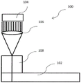
现在参照附图,其中,自始至终相似的参考号指代相同的部分,在图20A和21A的系统中可知用于切割衬底102的系统(通常用参考号100表示)。通常,系统100包括:激光器104;光学设备106,所述光学设备被定位在激光器的光路中用于以期望方式聚焦激光器的光;以及接口块108,所述接口块被定位成与衬底102成并置关系且位于如光学设备106所聚焦的激光器的光束的通路中。激光束安排、光学设备以及接口块与使用接口块的方法以及使用接口块的系统一起均在以下进行了更加详细的描述。然而,在描述此系统100之前且为了充分认识本发明,描述了本系统100中所采用的激光切割系统的示例实施例。Referring now to the drawings, wherein like reference numerals refer to like parts throughout, a system (generally designated by reference numeral 100) for cutting a
衬底的激光切割Laser cutting of substrates
在此描述的实施例涉及用于在透明材料中或穿过透明材料光学地产生高精密切割的方法和装置。表面下损伤可以被限制在60微米深度的量级或更小,并且切割仅可以产生少量碎屑。利用根据本公开的激光器切割透明材料还可以在此被称为钻孔或激光钻孔或激光加工。当在激光波长下的吸收是每毫米的材料深度小于约10%(优选小于约1%)时,材料对于此波长基本上是透明的。Embodiments described herein relate to methods and apparatus for optically producing high precision cuts in or through transparent materials. Subsurface damage can be limited to a depth of 60 microns or less, and cutting can produce only a small amount of debris. Cutting transparent materials with a laser according to the present disclosure may also be referred to herein as drilling or laser drilling or laser machining. When the absorption at the laser wavelength is less than about 10% (preferably less than about 1%) per millimeter of material depth, the material is substantially transparent to that wavelength.
根据以下描述的方法,在单次通过中,激光器可以被用于穿过材料产生高度受控的全线穿孔,而具有极小的(<75μm,常常<50μm)表面下损伤和碎屑产生。这与用于烧蚀材料的光斑聚焦激光器的典型使用形成对比,其中,多个通路经常需要完全地穿透玻璃厚度,从烧蚀过程中形成大量碎屑,并且发生更广泛的表面下损伤(>100μm)和边缘碎裂。According to the method described below, in a single pass, a laser can be used to create a highly controlled full-line perforation through a material with minimal (<75 μm, often <50 μm) subsurface damage and debris generation. This is in contrast to the typical use of spot focused lasers for ablation of materials, where multiple vias are often required to completely penetrate the glass thickness, a large amount of debris is formed from the ablation process, and more extensive subsurface damage occurs ( >100 μm) and edge chipping.
因此,使用单个高能量突发脉冲有可能在透明材料中产生微小的(即直径<0.5μm且>100nm)狭长的“孔”(也被称为穿孔或缺陷线)。这些单独的穿孔能够以数百千赫兹(例如,每秒数十万个穿孔)的速度产生。因此,在源与材料之间的相对运动下,这些穿孔可以彼此相邻放置(如所期望的,空间间隔从亚微米至数微米变化)。选择这种空间间隔以便有利于切割。在一些实施例中,缺陷线是“通孔”,所述“通孔”是从衬底材料的顶部至底部延伸的孔或开放通道。在一些实施例中,缺陷线不可以是连续的通道,并且可能被固体材料(例如,玻璃)的部分或者区段阻塞或部分地阻塞。如在此定义的,缺陷线的内直径是开放通道或气孔的内直径。例如,在此处描述的实施例中,缺陷线的内直径是<500nm(例如,<400nm)或者<300nm。在此处公开的实施例中围绕孔的材料的中断区域或改造区域(例如,压实的、熔融的、或以其他方式改变的)优选地具有<50μm的直径(例如,<0.10μm)。Thus, it is possible to create tiny (ie <0.5 μm in diameter and >100 nm in diameter) elongated “holes” (also known as perforations or defect lines) in transparent materials using a single high-energy burst. These individual perforations can be produced at hundreds of kilohertz (eg, hundreds of thousands of perforations per second). Thus, under relative motion between the source and the material, these perforations can be placed next to each other (as desired, with a spatial separation ranging from sub-micron to several microns). This spacing is chosen to facilitate cutting. In some embodiments, the defect lines are "vias," which are holes or open channels that extend from the top to the bottom of the substrate material. In some embodiments, the defect line may not be a continuous channel, and may be blocked or partially blocked by a portion or section of solid material (eg, glass). As defined herein, the inner diameter of a defect line is the inner diameter of an open channel or air hole. For example, in the embodiments described herein, the inner diameter of the defect line is <500 nm (eg, <400 nm) or <300 nm. Interrupted or modified regions (eg, compacted, melted, or otherwise altered) of the material surrounding the pores in the embodiments disclosed herein preferably have a diameter of <50 μm (eg, <0.10 μm).
此外,对透明材料的堆叠进行微加工和选择性切割是利用通过选择适当的激光源和波长连同光束传递光学器件对切割深进行精确控制以及对光束中断元件在希望的层的边界处进行布置而完成的。光束中断元件可以是材料层或界面。光束中断元件在此可以被称为激光束中断元件、中断元件等。光束中断元件的实施例在此可以被称为光束中断层、激光束中断层、中断层、光束中断界面、激光束中断界面、中断界面等。Furthermore, micromachining and selective dicing of stacks of transparent materials utilizes precise control of the depth of cut through selection of appropriate laser sources and wavelengths in conjunction with beam delivery optics and placement of beam interrupting elements at the boundaries of the desired layers. Completed. The beam breaking element can be a material layer or an interface. Beam interrupting elements may be referred to herein as laser beam interrupting elements, interrupting elements, or the like. Embodiments of beam breaking elements may be referred to herein as beam breaking layers, laser beam breaking layers, breaking layers, beam breaking interfaces, laser beam breaking interfaces, breaking interfaces, and the like.
光束中断元件反射、吸收、散射、散焦或以其他方式干涉入射激光束,以便抑制或防止激光束损伤或以其他方式修改堆叠中下面的层。在一个实施例中,光束中断元件位于其中将发生激光钻孔的透明材料层的下面。如在此使用的,当对光束中断元件的布置是使得激光束在遇到光束中断元件之前必须穿过透明材料时,光束中断元件位于透明材料的下面。光束中断元件可以位于其中将发生激光钻孔的透明层的下面并与所述透明层直接相邻。堆叠材料可以通过插入层或修改界面以高选择性进行微加工或切割,从而使得在堆叠的不同层之间存在光学特性的对比。通过使堆叠中的材料之间的界面在感兴趣的激光波长下更加反射、吸收、以及/或者散射,切割可以被限制在堆叠的一部分或一层。The beam interrupting element reflects, absorbs, scatters, defocuss, or otherwise interferes with the incident laser beam in order to inhibit or prevent laser beam damage or otherwise modify underlying layers in the stack. In one embodiment, the beam interruption element is located below the layer of transparent material in which the laser drilling will take place. As used herein, a beam interrupting element is located below the transparent material when the beam interrupting element is arranged such that the laser beam must pass through the transparent material before encountering the beam interrupting element. The beam breaking element may be located below and directly adjacent to the transparent layer in which the laser drilling will take place. Stacked materials can be micromachined or diced with high selectivity by intercalating layers or modifying interfaces so that there is a contrast in optical properties between the different layers of the stack. Cutting can be limited to a portion or layer of the stack by making the interface between the materials in the stack more reflective, absorbing, and/or scattering at the laser wavelength of interest.
选择激光的波长,从而使得待激光加工(钻孔、切割、烧蚀、损伤或通过激光器以其他方式明显改造)的堆叠内的材料对于所述激光波长而言是透明的。在一个实施例中,待通过激光加工的材料对于所述激光波长是透明的,如果它吸收小于10%的每毫米材料厚度的所述激光波长的强度。在另一个实施例中,待通过激光加工的材料对于所述激光波长是透明的,如果它吸收小于5%的每毫米材料厚度的所述激光波长的强度。在又另一个实施例中,待通过激光加工的材料对于所述激光波长是透明的,如果它吸收小于2%的每毫米材料厚度的所述激光波长的强度。在又另一个实施例中,待通过激光加工的材料对于所述激光波长是透明的,如果它吸收小于1%的每毫米材料厚度的所述激光波长的强度。The wavelength of the laser is selected such that the material within the stack to be laser processed (drilled, cut, ablated, damaged or otherwise significantly modified by the laser) is transparent to the laser wavelength. In one embodiment, the material to be processed by the laser is transparent to the laser wavelength if it absorbs less than 10% of the intensity of the laser wavelength per millimeter of material thickness. In another embodiment, the material to be laser processed is transparent to said laser wavelength if it absorbs less than 5% of the intensity of said laser wavelength per millimeter of material thickness. In yet another embodiment, the material to be laser processed is transparent to said laser wavelength if it absorbs less than 2% of the intensity of said laser wavelength per millimeter of material thickness. In yet another embodiment, the material to be laser processed is transparent to said laser wavelength if it absorbs less than 1% of the intensity of said laser wavelength per millimeter of material thickness.
激光源的选择进一步根据在透明材料中诱导多光子吸收(MPA)的能力。MPA是相同或不同频率的多个光子的同时吸收,以便将材料从较低能态(通常是基态)激发至较高能态(激发态)。激发态可以是激发电子态或电离态。材料的较高与较低能态之间的能量差等于两个或更多个光子的能量的总和。MPA是通常比线性吸收弱若干个数量级的三阶非线性过程。MPA与线性吸收的不同之处在于吸收的强度取决于光强度的平方,由此使其成为非线性光学过程。在普通的光强度下,MPA可忽略不计。如果光强度(能量密度)非常高(比如在激光源(特别是脉冲激光源)的焦点的区域中),则MPA变得明显并在区域内导致材料中的可测量的效应。而且,在焦点区域内,能量密度可以高到足以导致电离。The choice of laser source is further based on the ability to induce multiphoton absorption (MPA) in transparent materials. MPA is the simultaneous absorption of multiple photons of the same or different frequencies in order to excite a material from a lower energy state (usually the ground state) to a higher energy state (excited state). The excited state can be an excited electronic state or an ionized state. The energy difference between the higher and lower energy states of a material is equal to the sum of the energies of two or more photons. MPA is a third-order nonlinear process that is typically orders of magnitude weaker than linear absorption. MPA differs from linear absorption in that the intensity of absorption depends on the square of the light intensity, thus making it a nonlinear optical process. At ordinary light intensity, MPA is negligible. If the light intensity (energy density) is very high (such as in the region of the focal point of a laser source, especially a pulsed laser source), MPA becomes apparent and leads to measurable effects in the material in the region. Also, within the focal region, the energy density can be high enough to cause ionization.
在原子能级上,单个原子的电离具有离散能量需求。在玻璃中常用的几种元素(例如,Si、Na、K)具有相对低的电离能(约5eV)。在没有MPA现象的情况下,将需要约248nm的波长来产生约5eV下的线性电离。在具有MPA的情况下,由约5eV的能量分开的态之间的电离或激发可以用长于248nm的波长来完成。例如,具有532nm的波长的光子具有约2.33eV的能量,所以两个具有波长532nm的光子在双光子吸收(TPA)中可以诱发由约4.66eV的能量分开的态之间的跃迁。At atomic energy levels, the ionization of individual atoms has discrete energy requirements. Several elements commonly used in glass (eg, Si, Na, K) have relatively low ionization energies (about 5 eV). In the absence of the MPA phenomenon, a wavelength of about 248 nm would be required to produce linear ionization at about 5 eV. With MPA, ionization or excitation between states separated by energies of about 5 eV can be accomplished with wavelengths longer than 248 nm. For example, a photon with a wavelength of 532 nm has an energy of about 2.33 eV, so two photons with a wavelength of 532 nm can induce transitions between states separated by an energy of about 4.66 eV in two-photon absorption (TPA).
因此,在其中的激光束的能量密度高到足以诱导具有例如一半所需激发能量的激光波长的非线性TPA的材料区域中,原子和键可以被选择性地激发或电离。MPA可以导致激发的原子或键与相邻的原子或键的局部重构和分离。产生的键或构型的改造可以导致非热改造以及从其中发生MPA的材料区域中分离物质。这种改造或分离产生机械地削弱材料的结构缺陷(例如,缺陷线、或“穿孔”)并使其在施加机械或热应力时更容易破裂或断裂。通过控制穿孔的位置,可以精确地限定破裂发生所沿着的轮廓或路径,从而使得可以完成对材料的精细微加工。由一系列穿孔限定的轮廓可以被视为断裂线并对应于材料中的结构薄弱区域。在一个实施例中,微加工包括从激光器所加工的材料中分离出一部分,其中,所述部分具有由通过激光器所诱导的MPA作用形成的穿孔的闭合轮廓决定的精确限定的形状或外周。如在此使用的,术语闭合轮廓是指激光线形成的穿孔路径,其中,所述路径在某个位置与自身相交。内部轮廓是其中得到的形状完全由材料的外部部分围绕形成的路径。Thus, atoms and bonds can be selectively excited or ionized in regions of the material in which the energy density of the laser beam is high enough to induce nonlinear TPAs with, for example, half the laser wavelength of the desired excitation energy. MPA can lead to local reconfiguration and separation of excited atoms or bonds from neighboring atoms or bonds. The resulting modification of bonds or configurations can lead to non-thermal modification and separation of species from the region of the material where MPA occurs. This modification or separation creates structural defects (eg, defect lines, or "perforations") that mechanically weaken the material and make it more susceptible to cracking or breaking when mechanical or thermal stress is applied. By controlling the location of the perforations, the contour or path along which the rupture occurs can be precisely defined, allowing fine micromachining of the material to be accomplished. The contours defined by a series of perforations can be viewed as fracture lines and correspond to areas of structural weakness in the material. In one embodiment, micromachining includes separating a portion from the material processed by the laser, wherein the portion has a precisely defined shape or perimeter determined by the closed contour of the perforation formed by the action of the laser-induced MPA. As used herein, the term closed contour refers to a perforated path formed by a laser line, wherein the path intersects itself at a certain location. The inner contour is the path in which the resulting shape is completely surrounded by the outer portion of the material.
穿孔可以利用具有在时间上间隔很近的高能量短持续时间脉冲的单个“突发串”来完成。激光脉冲持续时间可以是10-10s或更短、或者10-11s或更短、或者10-12s或更短、或者10-13s或更短。这些“突发串”可以以高重复率(例如,kHz或MHz)进行重复。可以通过对激光器和/或衬底或堆叠的运动的控制来控制衬底或堆叠相对于激光器的速度从而间隔开并精确定位这些穿孔。Puncturing can be accomplished using a single "burst" of high energy short duration pulses that are closely spaced in time. The laser pulse duration can be 10-10 s or less, or 10-11 s or less, or 10-12 s or less, or 10-13 s or less. These "bursts" can be repeated at a high repetition rate (eg, kHz or MHz). These perforations can be spaced and precisely positioned by controlling the speed of the substrate or stack relative to the laser by controlling the motion of the laser and/or the substrate or stack.
作为示例,在暴露于一系列100kHz脉冲的以200毫米/秒移动的薄透明衬底中,单独脉冲将被间隔开2微米,以便产生被分隔开2微米的一系列穿孔。此缺陷(穿孔)间隔足够接近以便允许沿着所述一系列穿孔所限定的轮廓进行机械或热分离。As an example, in a thin transparent substrate moving at 200 mm/sec exposed to a series of 100 kHz pulses, the individual pulses would be spaced 2 microns apart to create a series of perforations separated by 2 microns. The defects (perforations) are spaced close enough to allow mechanical or thermal separation along the contours defined by the series of perforations.
热分离:Thermal separation:
在一些情况下,沿着一系列穿孔或缺陷线所限定的轮廓产生的断裂线并不足以自发地分离所述部分,并且第二步骤可能是必要的。如果希望的话,则例如可以使用第二激光器来产生热应力从而分离它。在蓝宝石的情况下,通过施加机械力或通过使用热源(例如,红外激光器,例如,CO2激光器)产生热应力并迫使一部分与衬底分离,在产生断裂线后,可以实现分离。另一种选择是使CO2激光器启动分离,并且,然后,使用手动技术完成分离过程。任选的CO2激光分离可以例如用散焦连续波(cw)激光器来实现,所述散焦连续波激光器在10.6μm处发射并且具有通过控制其占空比而进行调节的功率。焦点变化(即,散焦达到的程度并包括聚焦光斑尺寸)被用于通过改变光斑尺寸来改变诱导热应力。散焦激光束包括产生光斑尺寸的那些激光束,所述光斑尺寸大于激光波长尺寸数量级下的最小衍射极限的光斑尺寸。例如,约7mm、2mm以及20mm的光斑尺寸可以被用于CO2激光器,所述CO2激光器的发射波长在10.6μm处小的多。例如,在一些实施例中,沿着断裂线110的方向的相邻缺陷线120之间的距离可以大于0.5μm且小于或等于约15μm。In some cases, the fracture line created along the contour defined by a series of perforations or defect lines is not sufficient to separate the parts spontaneously, and a second step may be necessary. If desired, for example, a second laser can be used to generate thermal stress to separate it. In the case of sapphire, separation can be achieved after a fracture line is created by applying mechanical force or by using a heat source (eg, an infrared laser, eg, a CO2 laser) to generate thermal stress and force a portion to separate from the substrate. Another option is to have the CO laser initiate the separation and, then, use manual techniques to complete the separation process. Optional CO 2 laser separation can be achieved, for example, with a defocused continuous wave (cw) laser emitting at 10.6 μm and having a power regulated by controlling its duty cycle. The focus change (ie, the degree to which defocus is achieved and includes the focused spot size) is used to change the induced thermal stress by changing the spot size. Defocused laser beams include those that produce a spot size that is larger than the smallest diffraction-limited spot size in an order of magnitude of the laser wavelength size. For example, spot sizes of about 7mm, 2mm and 20mm can be used for CO2 lasers whose emission wavelength is much smaller at 10.6 μm. For example, in some embodiments, the distance between adjacent defect lines 120 in the direction of fracture line 110 may be greater than 0.5 μm and less than or equal to about 15 μm.
蚀刻:Etching:
例如,可以使用酸蚀刻例如来分离具有玻璃层的工件。为了将孔扩大至可用于金属填充和电连接的尺寸,部分可以被酸蚀刻。在一个实施例中,例如,所使用的酸可以是按体积计的10%HF/15%HNO3。例如,所述部分可以在24℃-25℃的温度下被蚀刻53分钟以便去除约100μm的材料。所述部分可以浸没在此酸浴中,并且在40kHz和80kHz频率的组合下的超声搅拌可以被用于促进在这些孔中的流体的渗透和流体交换。此外,可以在超声场内进行所述部分的人工搅拌以防止来自超声场的驻波图案在所述部分上产生“热点”或空穴相关的损伤。所述酸组合物和蚀刻速率可以有意地设计成用于缓慢地蚀刻所述部分——例如,仅1.9μm/分钟的材料去除速度。例如,小于约2μm/分钟的蚀刻速率允许酸充分渗透窄孔并且允许搅拌交换新鲜流体以及从最初非常窄的孔中去除溶解的材料。For example, acid etching can be used, for example, to separate workpieces having glass layers. Parts can be acid etched in order to enlarge the hole to a size that can be used for metal filling and electrical connection. In one embodiment, for example, the acid used may be 10% HF/15% HNO3 by volume. For example, the portion may be etched for 53 minutes at a temperature of 24°C-25°C to remove about 100 μm of material. The parts can be immersed in this acid bath, and ultrasonic agitation at a combination of 40 kHz and 80 kHz frequencies can be used to promote infiltration and fluid exchange of fluids in the pores. Additionally, manual agitation of the portion may be performed within the ultrasonic field to prevent the standing wave pattern from the ultrasonic field from creating "hot spots" or cavitation related damage on the portion. The acid composition and etch rate can be intentionally designed to etch the portion slowly - eg, a material removal rate of only 1.9 μm/min. For example, an etch rate of less than about 2 μm/min allows sufficient acid penetration of the narrow pores and allows agitation to exchange fresh fluid and remove dissolved material from the initially very narrow pores.
在图1中所示出的实施例中,对多层堆叠中的切割深度的精确控制通过包含光束中断界面(被标记为“改造界面”)来实现。光束中断界面防止激光辐射与超出中断界面的位置的部分多层堆叠相互作用。In the embodiment shown in Figure 1, precise control of the depth of cut in the multi-layer stack is achieved by the inclusion of a beam breaking interface (labeled "Remodeling Interface"). The beam interruption interface prevents the laser radiation from interacting with parts of the multilayer stack beyond the location of the interruption interface.
在一个实施例中,光束中断元件被定位在堆叠层的直接下方,在所述层中将发生经由双光子吸收的改造。这种构型在图1中示出,其中,光束中断元件是被定位在材料A的直接下方的改造界面并且材料A是在其中将通过在此描述的双光子吸收机制形成穿孔的材料。如在此使用的,参照在另一位置下方或低于另一位置的位置假定顶部或最上面的位置是激光束首先入射到其上的多层堆叠的表面。在图1中,例如,材料A最接近激光源的表面是顶表面并且光束中断元件在材料A下方的放置意味着激光束在与光束中断元件相互作用之前穿过材料A。In one embodiment, the beam breaking element is positioned directly below the stacked layers in which the modification via two-photon absorption will take place. This configuration is shown in Figure 1, where the beam breaking element is a retrofit interface positioned directly below Material A and Material A is the material in which the perforations will be formed by the two-photon absorption mechanism described herein. As used herein, reference to a position below or below another position assumes that the top or uppermost position is the surface of the multilayer stack on which the laser beam is first incident. In Figure 1, for example, the surface of material A closest to the laser source is the top surface and the placement of the beam breaking element below material A means that the laser beam passes through material A before interacting with the beam breaking element.
光束中断元件具有不同于待切割材料的光学特性。例如,光束中断元件可以是散焦元件、散射元件、半透明元件或者反射元件。散焦元件是包括防止激光在散焦元件上或散焦元件下方形成激光束焦线的材料的界面或层。散焦元件可以由具有散射或扰乱光束的波前的折射率不均匀性的材料或界面组成。半透明元件是材料的界面或层,所述材料允许光通过,但仅在散射或衰减激光束以便充分降低能量密度从而防止在半透明元件远离激光束的一侧的堆叠的部分中形成激光束焦线之后。在一个实施例中,半透明元件产生至少10%的激光束光线的散射或偏移。The beam interrupting element has different optical properties than the material to be cut. For example, the beam breaking element may be a defocusing element, a diffusing element, a translucent element or a reflective element. A defocusing element is an interface or layer that includes a material that prevents the laser from forming a focal line of the laser beam on or below the defocusing element. The defocusing element may be composed of materials or interfaces with refractive index inhomogeneities that scatter or disturb the wavefront of the beam. A translucent element is an interface or layer of material that allows light to pass through, but only scatters or attenuates the laser beam in order to reduce the energy density sufficiently to prevent laser beam formation on the side of the stack of translucent elements away from the laser beam after the focal line. In one embodiment, the translucent element produces a scattering or deflection of at least 10% of the light of the laser beam.
更具体地,可以采用中断元件的反射性、吸收性、散焦、衰减以及/或者散射来产生对激光辐射的屏障或障碍。激光束中断元件可以通过几种手段产生。如果整个堆叠系统的光学特性不重要,那么可以在期望的两层堆叠之间沉积一个或多个薄膜作为(多个)光束中断层,其中,所述一个或多个薄膜与在其直接上方的层相比吸收、散射、散焦、衰减、反射以及/或者消散更多的激光辐射,以便保护所述(多个)薄膜下方的层免于从激光源接收过多的能量密度。如果整个堆叠系统的光学特性的确重要,光束中断元件可以被实现为陷波滤波器。这可以通过几种方法来完成:More specifically, reflectivity, absorptivity, defocusing, attenuation, and/or scattering of the interrupting element may be employed to create a barrier or barrier to laser radiation. Laser beam interrupting elements can be created by several means. If the optical properties of the overall stack system are not critical, then one or more thin films can be deposited as the beam breaking layer(s) between the desired two-layer stack, wherein the one or more thin films are in contact with the directly above it The layers absorb, scatter, defocus, attenuate, reflect and/or dissipate more laser radiation than to protect the layers beneath the thin film(s) from receiving excessive energy density from the laser source. If the optical properties of the overall stacked system are indeed important, the beam interruption element can be implemented as a notch filter. This can be done in several ways:
·在中断层或界面处产生结构(例如,经由薄膜生长、薄膜图案化、或表面图案化),从而使得发生在特定波长或波长范围下的入射激光辐射上的衍射;creating structures at interrupted layers or interfaces (eg, via thin film growth, thin film patterning, or surface patterning) such that diffraction on incident laser radiation at a particular wavelength or range of wavelengths occurs;
·在中断层或界面处产生结构(例如,经由薄膜生长、薄膜图案化、或表面图案化),从而使得入射激光辐射发生散射(例如,纹理化的表面);creating structures at interrupted layers or interfaces (eg, via thin film growth, thin film patterning, or surface patterning) that scatter incident laser radiation (eg, textured surfaces);
·在中断层或界面处产生结构(例如,经由薄膜生长、薄膜图案化、或表面图案化),从而使得激光辐射发生衰减相移;以及Creation of structures at interrupted layers or interfaces (eg, via thin film growth, thin film patterning, or surface patterning) that allow for a decaying phase shift of the laser radiation; and
·在中断层或界面处经由薄膜堆叠产生分布式布拉格反射器以便反射激光辐射。• Creation of distributed Bragg reflectors via thin film stacks at interrupted layers or interfaces to reflect laser radiation.
由中断元件进行的激光束的吸收、反射、散射、衰减、散焦等没有必要是完整的。仅有必要的是,中断元件对激光束的影响足以将聚焦激光束的能量密度或强度降低至低于对中断元件所保护(在中断元件下面)的堆叠中的层进行切割、烧蚀、穿孔等所需要的阈值的水平。在一个实施例中,中断元件将聚焦激光束的能量密度或强度降低至低于诱导双光子吸收所需要的阈值的水平。中断层或中断界面可以被配置成用于吸收、反射或散射激光束,其中,所述吸收、反射或散射足以将传递至载体(或其他下面的层)的激光束的能量密度或强度降低至低于诱导载体层或下面的层中的非线性吸收所需水平的水平。Absorption, reflection, scattering, attenuation, defocusing, etc. of the laser beam by the interrupting element need not be complete. It is only necessary that the effect of the interrupting element on the laser beam is sufficient to reduce the energy density or intensity of the focused laser beam below that of cutting, ablating, perforating the layers in the stack protected by the interrupting element (underneath the interrupting element) etc. the desired threshold level. In one embodiment, the interruption element reduces the energy density or intensity of the focused laser beam to a level below the threshold required to induce two-photon absorption. The interrupted layer or interrupted interface can be configured to absorb, reflect or scatter the laser beam, wherein the absorption, reflection or scattering is sufficient to reduce the energy density or intensity of the laser beam delivered to the carrier (or other underlying layer) to A level below that required to induce nonlinear absorption in the carrier layer or in the underlying layer.
转向图2A和2B,激光钻孔材料的方法包括沿着光束传播方向观察到的将脉冲激光束2聚焦成激光束焦线2b。激光束焦线2b为高能量密度区域。如图3A中所示出的,激光器3(未示出)发射激光束2,所述激光束具有入射到光学组件6的一部分2a。光学组件6沿着光束方向(焦线的长度l)在限定的外延范围内的输出侧上将入射激光束转变为外延激光束焦线2b。Turning to Figures 2A and 2B, a method of laser drilling a material involves focusing a
层1是多层堆叠层,其中,通过激光加工和双光子吸收会发生内部改造。层1是更大工件的组件,所述组件典型地包括在其上形成多层堆叠的衬底或载体。层1是多层堆叠内的层,其中,孔、切口或其他特征将通过如在此描述的双光子吸收辅助的烧蚀或改造来形成。层1被定位在光束路径中以便至少部分地与激光束2的激光束焦线2b重叠。分别地,参考号1a表示层1面向(最靠近或邻近)光学组件6或激光器的表面,参考号1b表示层1的相反表面(与光学组件6或激光器离得远、或更远的表面)。层1的厚度(垂直于平面1a和1b(即,垂直于衬底平面)测量的)被标记为d。
如图2A描绘,层1垂直于纵向光束轴对齐并因此位于光学组件6所产生的相同焦线2b的后面(衬底垂直于附图的平面)。沿着光束方向观察,层1相对于焦线2b定位,其方式为使得焦线2b(在光束的方向上观察)在层1的表面1a之前开始并在层1的表面1b之前停止,即,焦线2b在层1内终止并且不延伸超出表面1b。在激光束焦线2b与层1的重叠区域中(即,在层1的被焦线2b重叠的部分中),外延激光束焦线2b在层1中产生非线性吸收。(假设沿着激光束焦线2b的适当激光强度,所述强度由激光束2在长度l的区段(即长度l的线状焦点)上的充分聚焦来保证,其限定了外延区段2c(沿着纵向光束方向对齐),沿着所述外延区段在层1中产生了诱导非线性吸收。)诱导非线性吸收导致沿着区段2c在层1中形成缺陷线或裂纹。缺陷线或裂纹的形成不仅是局部的,而且还可以在诱导吸收外延区段2c的整个长度上延伸。区段2c的长度(其对应于激光束焦线2b与层1重叠的长度)用参考号L标记。诱导吸收区段2c(或经历缺陷线或裂纹形成的层1的材料中的区段)的平均直径或平均延伸用参考号D标记。此平均延伸D基本上对应于激光束焦线2b的平均直径δ,即,在约0.1μm与约5μm之间的范围内的平均光斑直径。As depicted in Figure 2A,
如图2A所示,由于沿着焦线2b的诱导吸收,层1(其对于激光束2的波长λ而言是透明的)被局部加热。诱导吸收起因于与焦线2b内的激光束的高强度(能量密度)相关联的非线性效应。图2B展示了经加热的层1最终将膨胀,从而使得对应的诱导张力导致微裂纹形成,张力在表面1a处是最高的。As shown in Figure 2A, the
以下描述了可以被应用于产生焦线2b的代表性光学组件6以及这些光学组件可以被应用到其中的代表性光学装置。所有组件或装置均基于以上描述,从而使得相同的参考号被用于相同的块或特征或在其功能上相等的那些块或特征。因此,以下仅描述不同之处。Described below are representative
为了确保沿着一系列穿孔所限定的轮廓在破裂后分离表面的高质量(关于断裂强度、几何精度、粗糙度以及避免再加工需求),用于形成限定破裂轮廓的穿孔的单独焦线应当使用以下描述的光学组件产生(在下文中,光学组件还可替代地被称为激光光学器件)。经分离的表面的粗糙度主要由焦线的光斑尺寸或光斑直径决定。表面的粗糙度可以由例如Ra表面粗糙度统计数值(经采样的表面的高度绝对值的粗糙度算术平均值)来表征。为了在激光器3的给定波长λ的情况下(与层1的材料的相互作用)实现例如0.5μm至2μm的小光斑尺寸,某些要求通常必须强加在激光光学器件6的数值孔径上。这些要求由以下描述的激光光学器件6满足。In order to ensure a high quality (with regard to breaking strength, geometric accuracy, roughness and avoidance of re-machining needs) of the separation surface after fracture along the profile defined by the series of perforations, a separate focal line for forming the perforations defining the fracture profile should be used The optical assembly described below is produced (in the following, the optical assembly may alternatively be referred to as laser optics). The roughness of the separated surface is mainly determined by the spot size or spot diameter of the focal line. The roughness of the surface can be characterized, for example, by the Ra surface roughness statistic (the roughness arithmetic mean of the absolute value of the height of the sampled surface). In order to achieve a small spot size of eg 0.5 μm to 2 μm at a given wavelength λ of the laser 3 (interaction with the material of the layer 1 ) certain requirements must usually be imposed on the numerical aperture of the
为了实现所需要的数值孔径,光学器件一方面必须根据已知阿贝(Abbé)公式(N.A.=n sin(θ),n:待加工材料的折射率、θ:孔径角的一半、以及θ=arctan(D/2f);D:孔径、f:焦距)解决给定焦距所需要的开口。另一方面,激光束必须照射光学器件至所需要的孔径,这通常利用激光与聚焦光学器件之间的加宽望远镜借助于光束加宽来实现。In order to achieve the required numerical aperture, the optics must, on the one hand, be based on the known Abbé formula (N.A.=n sin(θ), n: the refractive index of the material to be processed, θ: half the aperture angle, and θ= arctan(D/2f); D: aperture, f: focal length) The opening required to address a given focal length. On the other hand, the laser beam has to irradiate the optics to the desired aperture, which is usually achieved by beam broadening using a broadening telescope between the laser and focusing optics.
为了沿焦线均匀相互作用的目的,光斑尺寸不应当改变太大。这可以例如通过仅在小的圆形区域中照射聚焦光学器件来确保(见以下实施例),从而使得光束开口以及因此数值孔径的百分比仅稍微改变。For the purpose of uniform interaction along the focal line, the spot size should not change too much. This can be ensured, for example, by illuminating the focusing optics only in a small circular area (see examples below), so that the percentage of beam opening and thus numerical aperture changes only slightly.
根据图3A(在激光辐射2的激光束丛中的中央光束的水平处垂直于衬底平面的区段;激光束2在此同样垂直入射到层1,即,入射角β为0°,从而使得焦线2b或诱导吸收延伸区段2c平行于衬底法线),激光器3发射的激光辐射2a首先被引导至对于所使用的激光辐射完全不透明的圆形光阑8上。光阑8垂直于纵向光束轴定向并且以描绘的光束丛2a的中央光束为中心。选择光阑8的直径,其方式为使得靠近光束丛2a的中心的光束丛或中心光束(在此用2aZ标记)撞击光阑并被其完全阻断。只有光束丛2a的外周范围内的光束(边缘光线,在此用2aR标记)由于与光束直径相比减小的光阑尺寸而未被阻断,而是侧向地穿过光阑8并撞击光学组件6(在此实施例中,其被设计为球形切割的双凸透镜7)的聚焦光学元件的边缘区域。According to FIG. 3A (segment perpendicular to the substrate plane at the level of the central beam in the laser beam bundle of the
透镜7以中心光束为中心并被设计为呈常见的球形切割透镜形式的未经校正的双凸聚焦透镜。这种透镜的球面像差可以是有利的。作为替代方案,也可以使用偏离理想校正系统的非球面透镜或多透镜系统,这些非球面透镜或多透镜系统未形成理想焦点而是形成了具有限定长度的不同狭长焦线(即,不具有单个焦点的透镜或系统)。透镜的区域因此沿焦线2b聚焦,受限于距透镜中心的距离。横越光束方向的光阑8的直径是光束丛的直径的约90%(由将光束的强度降低至峰值强度的1/e所需要的距离进行限定)并且是光学组件6的透镜的直径的约75%。因此使用通过阻挡掉中心的光束丛所产生的非像差校正球面透镜7的焦线2b。图3A示出了穿过中心光束的一个平面中的区段,当描绘的光束绕着焦线2b旋转时,可看到完整的三维丛。
这种类型的焦线的一个潜在的缺点是这些条件(光斑尺寸、激光强度)可能沿着焦线(以及因此沿着材料中的希望的深度)改变并且因此可能仅在焦线的选定部分中有可能发生期望类型的相互作用(无熔融、诱导吸收、热塑性形变直至裂纹形成)。这反过来意味着可能仅入射激光的一部分被待加工材料以期望的方式吸收。以这种方式,可能损害加工的效率(期望的分离速率所需要的平均激光功率),并且激光还可能被传输到非期望的区域(粘附到衬底或衬底保持夹具上的部分或层)并与它们以非期望的方式(例如,加热、扩散、吸收、不需要的改造)相互作用。A potential disadvantage of this type of focal line is that these conditions (spot size, laser intensity) may vary along the focal line (and thus along the desired depth in the material) and may therefore only be in selected parts of the focal line It is possible for the desired type of interaction to occur (no melting, induced absorption, thermoplastic deformation until crack formation). This in turn means that only a portion of the incident laser light may be absorbed in the desired manner by the material to be processed. In this way, the efficiency of the process (average laser power required for the desired separation rate) may be compromised, and the laser may also be transmitted to undesired areas (parts or layers that adhere to the substrate or substrate holding fixture). ) and interact with them in undesired ways (eg, heating, diffusion, absorption, unwanted remodeling).
图3B-1-4示出了(不仅针对图3A中的光学组件,还针对任何其他适用的光学组件6)可以通过相对于层1适当地定位和/或对齐光学组件6以及通过适当地选择光学组件6的参数来控制激光束焦线2b的位置。如图3B-1展示,焦线2b的长度l可以被调整,其方式为使得长度1超过层厚度d(在此为2倍)。如果层1被放置(沿着纵向光束方向观察)在焦线2b的中心,在整个衬底厚度上生成诱导吸收外延区段2c。Figures 3B-1-4 illustrate that (not only for the optical assembly in Figure 3A, but also for any other applicable optical assembly 6) that can be achieved by properly positioning and/or aligning the
在图3B-2中所示出的情况下,生成具有或多或少对应于层厚度d的长度1的焦线2b。由于层1相对于线2b定位,其方式为使得线2b在待加工材料外部的点处开始,因此,外延诱导吸收区段2c(在此,其从衬底表面延伸至限定的衬底深度,但不延伸至相反表面1b)的长度L比焦线2b的长度l小。图3B-3示出了衬底1(沿着光束方向观察)定位于焦线2b的起点上方的情况,从而使得如在图3B-2中线2b的长度l大于在层1中的诱导吸收区段2c的长度L。因此焦线在层1内开始并延伸超过相反表面1b。图3B-4示出了其中的焦线长度l小于层厚度d的情况,从而使得——在入射方向上观察到的衬底相对于焦线中央定位的情况下——焦线在层1内的表面1a附近开始并在层1内的表面1b附近结束(例如,l=0.75d)。例如,激光束焦线2b可以具有在约0.1mm与约100mm之间的范围内或在约0.1mm与约10mm之间的范围内的长度l。例如,不同实施例可以被配置为具有约0.1mm、0.2mm、0.3mm、0.4mm、0.5mm、0.7mm、1mm、2mm、3mm或5mm的长度l。In the case shown in Figure 3B-2, a
特别有利的是定位焦线2b,其方式为使得表面1a、1b中的至少一个表面被焦线覆盖,以便诱导非线性吸收区段2c至少在待加工的层或材料的一个表面上开始。以这种方式有可能实现几乎理想的切割,同时避免在表面上的烧蚀、羽化以及微粒化。It is particularly advantageous to position the
图4描绘了另一种可应用的光学组件6。基本构造遵循图3A中所描述的基本构造,因此,以下仅描述不同之处。所描绘的光学组件基于使用具有非球面自由表面的光学器件以便生成焦线2b,所述焦线被成形,其方式为使得形成具有限定长度l的焦线。为此目的,非球面透镜可以用作光学组件6的光学元件。在图4中,例如,使用也经常被称为轴锥镜的所谓的圆锥形棱镜。轴锥镜是沿光轴在线上形成光斑源(或将激光束转变为环)的特殊的圆锥形切割透镜。这种轴锥镜的布局对于本领域的技术人员来说原则上是已知的;在本实例中,锥角为10°。在此,用参考号9标记的轴锥镜的顶点指向入射方向并以光束中心为中心。由于轴锥镜9产生的焦线2b在其内部开始,因此,层1(在此,垂直于主光束轴对齐)可以被定位在光束路径中且位于轴锥镜9的正后方。如图4所示,还有可能由于轴锥镜的光学特性,沿光束方向移动层1,同时仍在焦线2b的范围内。层1的材料中的外延诱导吸收区段2c因此在整个深度d上延伸。FIG. 4 depicts another applicable
然而,所描绘的布局受制于以下限制:由于轴锥镜9形成的焦线2b的区域在轴锥镜9内开始,因此,在轴锥镜9与待加工材料之间存在间隔的情况下,激光能量的显著部分未被聚焦到焦线2b的诱导吸收区段2c(其位于所述材料内)中。此外,焦线2b的长度l通过轴锥镜9的折射率和锥角与光束直径有关。这是为什么,在相对薄的材料(数毫米)的情况下,总焦线比待加工材料的厚度长得多,从而具有许多激光能量没有聚焦到材料内的效应。However, the depicted layout is subject to the following limitation: Since the area of the
为此,可能希望使用包括轴锥镜和聚焦透镜两者的光学组件6。图5A描绘了此类光学组件6,在所述光学组件中,具有被设计成用于形成外延激光束焦线2b的非球面自由表面的第一光学元件(沿光束方向观察)被定位在激光器3的光束路径中。在图5A中所示出的情况下,此第一光学元件是具有5°锥角的轴锥镜10,所述轴锥镜垂直于光束方向定位并以激光束3为中心。轴锥镜的顶点被定向成朝向光束方向。在此为平凸透镜11(其弯曲朝向轴锥镜定向)的第二聚焦光学元件被定位在光束方向上与轴锥镜10相距距离Z1。选择距离Z1(在这种情况下约300mm),其方式为使得轴锥镜10形成的激光辐射圆形地入射到透镜11的外部径向部分上。透镜11将圆形辐射聚焦在具有限定长度(在此情况下为1.5mm)的焦线2b的距离Z2(在此情况下距透镜11约20mm)处的输出侧上。在此实施例中,透镜11的有效焦距为25mm。激光束通过轴锥镜10的圆形变换被标记为参考号SR。For this purpose, it may be desirable to use an
图5B详细描绘了根据图5A的层1的材料中的焦线2b或诱导吸收2c的形成。选择元件10、11两者的光学特性及其定位,其方式为使得在光束方向上的焦线2b的长度l与层1的厚度d完全相同。因此,需要沿光束方向精确定位层1,以便如图5B中所示出的将焦线2b精确定位在层1的两个表面1a与1b之间。Figure 5B depicts in detail the formation of
因此,如果在距激光光学器件一定距离处形成焦线,并且如果激光辐射的更大部分聚焦到焦线期望的末端,则是有利的。如所描述的,这可以通过仅将主要聚焦元件11(透镜)圆形地(环形地)照射在特定外部径向区域上来实现,这一方面用于实现所需要的数值孔径以及因此所需要的光斑尺寸,并且,然而,在另一方面,由于形成了基本上圆形的光斑,所以漫射的圆在光斑的中心的非常短的距离上所需要的焦线2b之后强度减小。以此方式,裂纹的形成在所需要的衬底深度的短距离内停止。轴锥镜10与聚焦透镜11的组合满足此要求。轴锥镜以两种不同方式起作用:由于轴锥镜10的原因,通常圆形的激光光斑以环的形状发送到聚焦透镜11,并且轴锥镜10的非球面性具有在透镜的焦面(而非焦面中的焦点)之外形成焦线的效应。焦线2b的长度l可以借助于轴锥镜上的光束直径进行调节。沿焦线的数值孔径在另一方面可以借助于轴锥镜-透镜距离Z1并借助于轴锥镜的锥角进行调节。以此方式,全部的激光能量可以集中在焦线中。Therefore, it is advantageous if the focal line is formed at a distance from the laser optics, and if a larger portion of the laser radiation is focused to the desired end of the focal line. As described, this can be achieved by only illuminating the primary focusing element 11 (lens) circularly (annularly) on a certain outer radial area, in this regard for achieving the required numerical aperture and therefore the required The spot size, and, however, on the other hand, since a substantially circular spot is formed, the diffuse circle is reduced in intensity after the required
如果裂纹形成旨在持续到待加工的层或材料的背面,圆形(环形)照射仍然具有以下优点:(1)在大部分激光仍然集中在焦线所需要的长度中的意义下,激光功率使用得最佳,以及(2)沿焦线有可能实现均匀的光斑尺寸——以及因此沿焦线产生的穿孔的均匀分离过程——由于圆形照射区域结合借助于其他光学功能设定的期望像差的原因。If crack formation is intended to continue to the backside of the layer or material to be processed, circular (ring) irradiation still has the following advantages: (1) Laser power in the sense that most of the laser is still concentrated in the required length of the focal line Used optimally, and (2) it is possible to achieve a uniform spot size along the focal line - and thus a uniform separation process of the perforations produced along the focal line - due to the circular illumination area combined with the expectations set by means of other optical functions cause of aberrations.
代替图5A中所描绘的平凸透镜,还有可能使用聚焦弯月形透镜或另一种更高校正聚焦透镜(非球面透镜、多透镜系统)。Instead of the plano-convex lens depicted in Figure 5A, it is also possible to use a focusing meniscus lens or another higher correcting focusing lens (aspheric lens, multi-lens system).
为了使用图5A中所描绘的轴锥镜与透镜的组合生成非常短的焦线2b,将有必要选择入射到轴锥镜上的激光束的非常小的光束直径。这具有实际的缺点:必须非常精确地将光束的中心确定在轴锥镜顶点上,并且所述结果对激光器的方向变化(光束漂移稳定性)非常敏感。此外,紧密准直激光束非常发散,即,由于光偏转的原因,光束丛在短距离内变得模糊。In order to generate a very short
如图6中所示出的,通过在光学组件6中包括另一个透镜(准直透镜12),两种效应均可以避免。附加的正透镜12用于非常紧密地调整聚焦透镜11的圆形照射。选择准直透镜12的焦距f',其方式为使得期望的等于f'的圆直径dr由从轴锥镜到准直透镜12的距离Z1a产生。期望的环的宽度br可以经由距离Z1b(准直透镜12到聚焦透镜11)进行调节。由于纯粹几何学的原因,小的圆形照射宽度导致了较短的焦线。最小值可以在距离f'处实现。By including another lens (collimating lens 12) in the
图6中所描绘的光学组件6因此基于图5A中所描绘的光学组件,因此以下仅描述了不同之处。在此还被设计为平凸透镜(其曲率朝向光束方向)的准直透镜12另外地居中放置在一侧的轴锥镜10(其顶点朝向射束方向)与另一侧的平凸透镜11之间的光束路径中。准直透镜12距轴锥镜10的距离被称为Z1a,聚焦透镜11距准直透镜12的距离被称为Z1b,并且焦线2b距聚焦透镜11的距离被称为Z2(始终在光束方向上观察)。如图6中所示出的,轴锥镜10形成的圆形辐射SR(其发散地并且在圆直径dr下入射到准直透镜12上)针对在聚焦透镜11处至少近似恒定的圆直径dr被调整成沿距离Z1b所需要的圆宽度br。在所示出的情况下,旨在生成非常短的焦线2b,从而使得透镜12处的大约4mm的圆宽度br由于透镜12的聚焦特性而在透镜11处减少到约0.5mm(在此示例中,圆直径dr为22mm)。The
在所描绘的示例中,使用2mm的典型激光束直径、具有焦距f=25mm的聚焦透镜11、具有焦距f’=150mm的准直透镜以及选择距离Z1a=Z1b=140mm和Z2=15mm有可能实现焦线l的长度小于0.5mm。In the depicted example, it is possible to achieve using a typical laser beam diameter of 2mm, a focusing
注意,如图7中所示出的,这种皮秒激光器的典型操作产生脉冲720的“突发串”710。每个“突发串”710可以包含具有非常短的持续时间(约10皮秒)的多个脉冲720(比如,至少2个脉冲,或者如在图7中所示出的至少3个脉冲(例如,4个脉冲、5个脉冲或更多))。(爆发或产生脉冲突发串是激光操作的一类,其中,脉冲的发射并非呈均匀且稳定的流,而是呈紧凑的脉冲簇。)脉冲720具有最高达100皮秒(例如,0.1皮秒、5皮秒、10皮秒、15皮秒、18皮秒、20皮秒、22皮秒、25皮秒、30皮秒、50皮秒、75皮秒或介于它们之间)的脉冲持续时间Td。优选地,突发串内的每个脉冲720以在约1纳秒与约50纳秒之间(例如。10-50纳秒或者10-30纳秒)的范围内的持续时间Tp在时间上分离,所述时间经常由激光腔设计调控)。对于给定激光器,突发串710内的相邻脉冲之间的时间间隔Tp(脉冲到脉冲的间隔)可以相当均匀(±10%)。例如,在一些实施例中,突发串内的每个脉冲与随后的脉冲在时间上间隔约20纳秒(50MHz)。例如,对于产生约20纳秒的脉冲间隔Tp的激光器,突发串内的脉冲到脉冲间隔Tp维持在约±10%内或约±2纳秒内。对于约100kHz的激光重复率,每个“突发串”710之间的时间将会更长(例如,0.25<Tb<1000微秒,例如,1-10微秒或者3-8微秒)(经常为约10微秒)。确切的定时、脉冲持续时间以及重复率可以根据激光设计而改变,但高强度的短脉冲(<约15皮秒)已经被示出用于与此技术很好地一起工作。Note that typical operation of such a picosecond laser produces a "burst" 710 of
在此所描述的激光器的一些示例性实施例中,对于具有约200kHz的突发串重复率或频率的激光器,时间间隔Tb为约5微秒。激光突发串重复率和突发串的第一脉冲与随后的突发串的第一脉冲之间的时间Tb有关(激光突发串重复率=1/Tb)。在一些实施例中,激光突发串重复频率可以在约1kHz与约4MHz之间的范围内。在另一个实施例中,激光突发串重复率可以例如在约10kHz与650kHz之间的范围内。每个突发串的第一脉冲与随后的突发串的第一脉冲之间的时间Tb可以为0.25微秒(4MHz突发串重复率)至1000微秒(1kHz突发串重复率)(例如,0.5微秒(2MHz突发串重复率)至40微秒(25kHz突发串重复率)或者2微秒(500kHz突发串重复率)至20微秒(50kHz突发串重复率))。确切的定时、脉冲持续时间以及串重复率可以根据激光设计来改变,但高强度的短脉冲(Td<20皮秒,并且优选地,Td≤15皮秒)已经被示出用于特别良好地进行工作。In some exemplary embodiments of the lasers described herein, the time interval T b is about 5 microseconds for lasers having a burst repetition rate or frequency of about 200 kHz. The laser burst repetition rate is related to the time T b between the first pulse of a burst and the first pulse of a subsequent burst (laser burst repetition rate = 1/T b ). In some embodiments, the laser burst repetition frequency may range between about 1 kHz and about 4 MHz. In another embodiment, the laser burst repetition rate may range, for example, between about 10 kHz and 650 kHz. The time T b between the first pulse of each burst and the first pulse of the subsequent burst may be 0.25 microseconds (4MHz burst repetition rate) to 1000 microseconds (1 kHz burst repetition rate) (For example, 0.5µs (2MHz burst repetition rate) to 40µs (25kHz burst repetition rate) or 2µs (500kHz burst repetition rate) to 20µs (50kHz burst repetition rate) ). The exact timing, pulse duration, and train repetition rate can vary depending on the laser design, but high intensity short pulses (T d < 20 picoseconds, and preferably T d ≤ 15 picoseconds) have been shown for particular Work well.
使用能够产生此类脉冲突发串的激光器有利于切割或改造透明材料(例如,玻璃)。与使用由单脉冲激光器的重复率在时间上间隔开的单个脉冲相比,使用脉冲突发串序列(其将激光能量散布在突发串710内的快速脉冲序列)允许获得与材料的高强度相互作用的更大的时间尺度(与和单脉冲激光器的高强度相互作用可能获得的时间尺度相比)。虽然单脉冲可以在时间上扩展,但若这样做,脉冲内的强度必须下降约脉冲宽度分之一。因此,如果10皮秒单个脉冲的脉冲长度扩展至10纳秒,强度将下降约三个数量级。这种下降可以将光学强度减少到非线性吸收不再显著的点,并且光/材料相互作用不再强到足以允许切割所述材料。相比之下,在脉冲突发串激光器下,突发串710内的每个脉冲720期间的强度可以维持得非常高——例如,在时间上间隔开约10纳秒的三个10皮秒脉冲720仍允许每个脉冲内的强度比单个10皮秒脉冲的强度高约3倍,同时允许所述激光器在比现在大三个数量级的时间尺度内与所述材料相互作用。在突发串710内的多个脉冲720的这一调节因此允许按以下方式操纵激光器-材料相互作用的时间尺度,这些方式可以促进更多或更少的与预先存在的等离子体羽之间的相互作用、更多或更少的与已由初始或先前的激光脉冲预激励的原子和分子之间的光-材料相互作用、以及可以促进微裂纹的受控制的增长的所述材料内的更多或更少的热效应。用于对材料进行改造所需要的突发串能量的量将取决于衬底材料成分以及用于与所述衬底相互作用的线状焦点的长度。相互作用区越长,能量散布出去的越多,并且将需要越高的突发串能量。确切的定时、脉冲持续时间以及突发串重复率可以根据激光设计进行改变,但高强度的短脉冲(<15皮秒,或≤10皮秒)已经被示出用于与此技术很好地一起工作。当单个脉冲突发串撞击玻璃上的基本上同一位置时,在材料中形成缺陷线或孔。即,单个脉冲突发串内的多个激光脉冲对应于玻璃中的单个缺陷线或孔位置。当然,由于玻璃平移(例如,通过不断移动的平台)(或光束相对于玻璃移动),脉冲突发串内的单独脉冲不可能位于玻璃上的完全相同的空间位置处。然而,它们彼此很好地处于1μm内——即,它们在基本上相同的位置撞击玻璃。例如,它们可以按彼此之间的间隔sp来撞击玻璃,其中,0<sp<500nm。例如,当用20个脉冲的脉冲突发串710击中玻璃位置时,脉冲突发串710内的单独脉冲720在彼此的250nm内撞击玻璃。因此,在一些实施例中,1nm<sp<250nm。在一些实施例中,1nm<sp<100nm。The use of lasers capable of generating such bursts of pulses is advantageous for cutting or modifying transparent materials (eg, glass). Using a pulse burst sequence, which spreads the laser energy within the
图8示出了入射到玻璃-空气-玻璃复合结构上的聚焦高斯光束与贝塞尔光束之间的对比(在图8中,高斯光束示出在左侧并且贝塞尔光束示出在右侧)。聚焦高斯光束被示出用于一进入第一玻璃层就进行偏离并且不钻孔穿过第一玻璃层。在第二示例中,示出在高斯光束的右侧,由于自聚焦的发生,第一玻璃层被分叉。当发生自聚焦时(在玻璃被钻孔时),光束从第一玻璃层中露出并发生衍射。因此,光束将不会钻入到第二玻璃层中。进一步移动到图8中的右侧,贝塞尔光束能够在线状焦点的整个长度上对两层玻璃层充分钻孔。在这一示例中,衬底是玻璃-空气-玻璃复合结构。顶部和底部玻璃片为0.4mm厚的2320,CT101。两层玻璃之间的示例性空气间隙为约400μm。以200mm/秒用激光的单次通过进行切割,从而使得这两片玻璃被同时切割,即使它们被分隔开>400μm。Figure 8 shows a comparison between a focused Gaussian beam and a Bessel beam incident on a glass-air-glass composite structure (in Figure 8, the Gaussian beam is shown on the left and the Bessel beam is shown on the right side). A focused Gaussian beam is shown for deflection as soon as it enters the first glass layer and does not drill through the first glass layer. In the second example, shown to the right of the Gaussian beam, the first glass layer is bifurcated due to the occurrence of self-focusing. When self-focusing occurs (when the glass is drilled), the beam emerges from the first glass layer and diffracts. Therefore, the beam will not drill into the second glass layer. Moving further to the right in Figure 8, the Bessel beam is able to sufficiently drill both glass layers over the entire length of the linear focus. In this example, the substrate is a glass-air-glass composite structure. The top and bottom glass sheets are 0.4mm thick 2320, CT101. An exemplary air gap between two layers of glass is about 400 μm. Cutting was performed with a single pass of the laser at 200 mm/sec, so that the two pieces of glass were cut simultaneously, even though they were separated by >400 μm.
在此处描述的部分实施例中,空气间隙可以是任何合适的距离,如例如在50μm与5mm之间、在50μm与2mm之间或者在200μm与2mm之间。In some of the embodiments described herein, the air gap may be any suitable distance, such as, for example, between 50 μm and 5 mm, between 50 μm and 2 mm, or between 200 μm and 2 mm.
示例性中断层包括聚乙烯塑料板(例如,Visqueen)。如在图9中所示出的透明层包括透明乙烯树脂(例如,Penstick)。注意,不像使用其他聚焦激光方法,为了获得阻断或停止层的效果,不需要精确地控制准确焦点,中断层的材料也不需要是特别耐用的或昂贵的。在许多应用中,层只需要稍微干涉激光以便中断激光并防止产生线状焦点。Visqueen防止用皮秒激光器和线状焦点进行切割的事实是很好的例子——其他聚焦皮秒激光束将十分肯定地进行钻孔直接穿过Visqueen,并且若希望用其他激光方法避免进行钻孔直接穿过这种材料,人们将不得不非常精确地将激光焦点设定为不靠近Visqueen。Exemplary disruption layers include polyethylene plastic sheets (eg, Visqueen). The transparent layer as shown in FIG. 9 includes transparent vinyl (eg, Penstick). Note that, unlike using other focused laser methods, precise focus control does not need to be precisely controlled in order to obtain the effect of the blocking or stopping layer, nor does the material of the interrupting layer need to be particularly durable or expensive. In many applications, the layer only needs to interfere with the laser light slightly in order to interrupt the laser light and prevent the creation of a linear focus. The fact that Visqueen prevents cutting with picosecond lasers and line focal points is a good example - other focused picosecond laser beams will certainly drill directly through Visqueen and avoid drilling with other laser methods if desired Going straight through this material, one would have to set the laser focus very precisely not close to the Visqueen.
图10示出了堆叠有透明保护层以便切割多个板,同时减小磨损或污染。同时切割显示玻璃板堆叠是非常有利的。透明聚合物如乙烯树脂可以被放置在玻璃板之间。透明聚合物层是用于降低对彼此紧密接触的玻璃表面的损伤的保护层。这些层将会允许运行切割过程,但将会保护玻璃板免于划伤彼此,并且将会进一步防止任何切割碎屑(尽管使用此过程的情况下切割碎屑很小)污染玻璃表面。保护层也可以由沉积在衬底或玻璃板上的蒸发介电层组成。Figure 10 shows the stacking of a transparent protective layer for cutting multiple boards while reducing wear or contamination. It is very advantageous to cut the stack of display glass sheets at the same time. A transparent polymer such as vinyl can be placed between the glass plates. The transparent polymer layer is a protective layer for reducing damage to glass surfaces that are in close contact with each other. These layers will allow the cutting process to run, but will protect the glass sheets from scratching each other and will further prevent any cutting debris (albeit small with this process) from contaminating the glass surface. The protective layer can also consist of an evaporated dielectric layer deposited on a substrate or glass plate.
参照图11,展示了一种切割堆叠组件中的切孔图案的方法。此线状焦点过程可以同时切穿堆叠的玻璃板,即使存在显著的肉眼可见的空气间隙。这使用其他激光方法(如在图8中所展示的高斯光束)是不可能的。许多设备需要玻璃封装,比如,OLED(有机发光二极管)。能够同时切穿两层玻璃是非常有利的,因为它提供了可靠且有效的设备分割过程。分割是指将一个组件从可以包含多个其他组件的较大的材料板中分离的过程。可以通过在此描述的方法分割、切去或者生产的其他组件是例如OLED(有机发光二极管)组件、DLP(数字光处理器)组件、LCD(液晶显示器)单元、半导体设备衬底。Referring to Figure 11, a method of cutting a hole pattern in a stacked assembly is shown. This line-of-focus process can simultaneously cut through stacked glass sheets, even in the presence of significant macroscopic air gaps. This is not possible using other laser methods such as the Gaussian beam shown in Figure 8. Many devices require glass encapsulation, eg, OLEDs (Organic Light Emitting Diodes). Being able to cut through two layers of glass at the same time is very advantageous as it provides a reliable and efficient device segmentation process. Splitting is the process of separating one component from a larger sheet of material that can contain multiple other components. Other components that can be divided, cut or produced by the methods described herein are eg OLED (Organic Light Emitting Diode) components, DLP (Digital Light Processor) components, LCD (Liquid Crystal Display) cells, semiconductor device substrates.
参照图12,展示了切割如涂覆有透明导电层(例如,ITO)的电致变色玻璃的物品的过程。切割已经具有透明导电层(比如氧化铟锡(ITO))的玻璃对于电致变色玻璃应用以及对于触摸面板设备应用具有很高价值。在此所描述的激光过程可以切穿这种层,而对透明导电层的损伤最小并产生很少的碎屑。穿孔的极小尺寸(<5um)意味着非常少的ITO将受到切割过程的影响,而其他切割方法将要产生多得多的表面损伤和碎屑。Referring to Figure 12, a process for cutting an article such as electrochromic glass coated with a transparent conductive layer (eg, ITO) is shown. Cutting glass that already has a transparent conductive layer such as indium tin oxide (ITO) is of great value for electrochromic glass applications as well as for touch panel device applications. The laser process described herein can cut through such layers with minimal damage to the transparent conductive layer and generation of very little debris. The extremely small size (<5um) of the perforations means that very little ITO will be affected by the cutting process, while other cutting methods will generate much more surface damage and debris.
参照图13,公开了一种用于对堆叠中的一些层进行精密切割而不损伤其他层的方法。虽然此方法也示出在图1中,但是图13的实施例将所述概念延伸至多个层(即,两层以上)。在图13的实施例中,中断元件是散焦层。Referring to Figure 13, a method for precision cutting some layers in a stack without damaging other layers is disclosed. Although this approach is also shown in Figure 1, the embodiment of Figure 13 extends the concept to multiple layers (ie, more than two layers). In the embodiment of Figure 13, the interrupting element is a defocus layer.
总之且通常,然后,切割机制基本上如在图14A中所示出的,并且用于切割和分离透明衬底的方法基本上基于用超短脉冲激光器在待加工衬底上生成断裂线。根据材料特性(吸收、CTE、应力、组成等)以及被选择用于处理所确定的衬底的激光参数,单独产生断裂线足以诱发自分离,并且在这一情况下无需二次处理(比如弯曲力/张力或CO2激光器)。In summary and generally, then, the cutting mechanism is substantially as shown in Figure 14A, and the method for cutting and separating transparent substrates is basically based on generating fracture lines on the substrate to be processed with an ultrashort pulsed laser. Depending on the material properties (absorption, CTE, stress, composition, etc.) and the parameters of the laser selected to process the determined substrate, the creation of fracture lines alone is sufficient to induce self-separation, and in this case no secondary processing (such as bending is required) force/tension or CO2 laser).
然而,在一些情况下,所产生的断裂线并不足以自动分离衬底并且二次步骤可能是必要的。如果是这样,例如可以使用第二激光器以产生热应力从而分离衬底。在2320NIOX的具体且规范的情况下,已经发现,通过机械力的应用或通过使用第二CO2激光器来产生热应力并迫使这些部分进行自分离可以在产生缺陷线后实现分离。另一种选择是使CO2激光器只启动分离并手动完成分离。任选的CO2激光分离用聚焦cw激光器来实现,所述聚焦cw激光器在10.6μm处发射且具有通过控制其占空比进行调节的功率。焦点变化被用于通过改变光斑尺寸来改变诱导热应力。However, in some cases the resulting fracture lines are not sufficient to automatically separate the substrates and a secondary step may be necessary. If so, for example a second laser can be used to generate thermal stress to separate the substrates. In the specific and normative case of 2320NIOX, it has been found that separation can be achieved after defect lines are created by the application of mechanical force or by using a second CO2 laser to generate thermal stress and force the parts to self-separate. Another option is to have the CO2 laser just start the separation and do it manually. The optional CO 2 laser separation was achieved with a focused cw laser emitting at 10.6 μm and with power regulated by controlling its duty cycle. Focus changes were used to alter the induced thermal stress by changing the spot size.
有几种方法用于产生缺陷线。形成线状焦点的光学方法可以采取多种形式,使用环状激光束和球面透镜、轴锥透镜、衍射元件或其他方法来形成高强度的线性区域。激光器的类型(皮秒、飞秒等)和波长(IR、绿色、UV等)也可以改变,只要达到充分的光学强度分解衬底材料。There are several methods for generating defective lines. Optical methods for creating linear focal points can take many forms, using annular laser beams and spherical lenses, axicons, diffractive elements, or other methods to create linear regions of high intensity. The type of laser (picosecond, femtosecond, etc.) and wavelength (IR, green, UV, etc.) can also be varied as long as sufficient optical intensity is achieved to decompose the substrate material.
在使用本发明的实验中,超短脉冲激光器被用于以一致、可控且可重复的方式来产生高纵横比的竖直缺陷线。如以上所描述的,此概念的本质是利用超短(皮秒或飞秒持续时间)贝塞尔光束使用光学透镜组件中的轴锥透镜元件来产生高纵横比的无锥度的微通道。换言之,轴锥镜将激光束聚光到具有圆柱形状和高纵横比(较长的长度和较短的直径)的区域中。由于用聚光激光束产生的高强度的原因,发生激光电磁场与材料之间的非线性相互作用并且激光能量被转移到衬底上。然而,重要的是认识到,在激光能量强度不高的区域(即,玻璃表面、围绕中心会聚线的玻璃体积)中,因为激光强度低于非线性阈值,玻璃不会发生任何事情。In experiments using the present invention, ultrashort pulsed lasers were used to generate high aspect ratio vertical defect lines in a consistent, controllable and repeatable manner. As described above, the essence of this concept is to utilize ultrashort (picosecond or femtosecond duration) Bessel beams to create high aspect ratio taper-free microchannels using axicon lens elements in an optical lens assembly. In other words, the axicon focuses the laser beam into a region with a cylindrical shape and a high aspect ratio (longer length and shorter diameter). Due to the high intensity generated with the concentrated laser beam, nonlinear interactions between the laser electromagnetic field and the material occur and the laser energy is transferred to the substrate. However, it is important to realize that in regions where the laser energy intensity is not high (ie, the glass surface, the glass volume around the central convergence line), because the laser intensity is below the nonlinear threshold, nothing will happen to the glass.
图2A-2C展示了处于不同激光强度状态的激光-物质相互作用。在第一种情况下,未聚焦的激光束穿过透明衬底而未对其引入任何改造。在此特定情况下,不存在非线性效应,因为激光能量密度(或被光束照射的每单位面积激光能量)低于诱发非线性效应所需要的阀值。能量密度越高,电磁场的强度越强。因此,当激光光束聚焦成较小的光斑尺寸时,照射面积减小并且能量密度增加,触发非线性效应,所述非线性效应将只对满足所述条件的体积的材料进行改造。以此方式,如果聚焦激光器的束腰被定位在衬底表面,则将在此处出现损伤。反之,如果聚焦激光的束腰被定位在衬底表面的下方,因为能量密度低于非线性光学效应的阀值,所以表面不会发生任何事情。但在定位于大块衬底中的焦点处,激光强度足以触发多光子效应并诱发对材料的损伤。最后,在轴锥镜的情况下,轴锥透镜或可替代地菲涅耳(Fresnel)轴锥镜的衍射图案产生干扰,所述干扰产生贝塞尔状强度分布(高强度圆柱),并且只有以这种体积才具有足够的强度以产生非线性吸收并对材料进行改造。2A-2C illustrate laser-matter interactions at different laser intensity states. In the first case, the unfocused laser beam passes through the transparent substrate without introducing any modification to it. In this particular case, there is no nonlinear effect because the laser fluence (or laser energy per unit area irradiated by the beam) is below the threshold required to induce nonlinear effects. The higher the energy density, the stronger the strength of the electromagnetic field. Thus, when the laser beam is focused to a smaller spot size, the irradiated area is reduced and the energy density is increased, triggering nonlinear effects that will only modify the volume of material that satisfies the condition. In this way, if the beam waist of the focused laser is positioned at the substrate surface, damage will occur there. Conversely, if the beam waist of the focused laser is positioned below the substrate surface, nothing will happen to the surface because the energy density is below the threshold for nonlinear optical effects. But at the focal point positioned in the bulk substrate, the laser intensity is sufficient to trigger the multiphoton effect and induce damage to the material. Finally, in the case of an axicon, the diffraction pattern of an axicon or alternatively a Fresnel axicon produces interference which produces a Bessel-like intensity distribution (a cylinder of high intensity) and only In this volume it is strong enough to generate nonlinear absorption and modify the material.
激光器和光学系统:Lasers and Optical Systems:
出于切割玻璃的目的,开发了使用1064nm皮秒激光器结合线状焦点聚束光学系统来产生衬底中的损伤线的过程。定位0.7mm厚的玻璃衬底,从而使得所述玻璃衬底处于线状焦点内。利用约1mm长的线状焦点以及以200kHz(约100μ/脉冲)的重复率产生至少24W的输出功率的皮秒激光器,然后,线性区域中的光学强度可以轻易地高到足以在材料中产生非线性吸收。产生大致仿效高强度线性区域的损伤的、烧蚀的、汽化的或以其他方式进行改造的材料区域。For the purpose of cutting glass, a process was developed to generate damage lines in the substrate using a 1064 nm picosecond laser in combination with a linear focus beamforming optical system. A 0.7 mm thick glass substrate is positioned so that it is within the line focus. With a linear focus of about 1 mm long and a picosecond laser producing at least 24 W of output power at a repetition rate of 200 kHz (about 100 μ/pulse), the optical intensity in the linear region can then easily be high enough to produce non-uniformity in the material. Linear absorption. A damaged, ablated, vaporized, or otherwise modified region of material is created that substantially emulates a high-strength linear region.
值得注意的是,这种皮秒激光器的典型操作产生了脉冲“突发串”。每个“突发串”可以包含具有非常短的持续时间(例如,约10皮秒)的多个次脉冲。每个次脉冲在时间上隔开例如约20纳秒(50MHz),所述时间经常由激光腔设计调控。对于约200kHz的激光重复率而言,每个“突发串”之间的时间将更长(经常为约5微秒)。精确的定时、脉冲持续时间以及重复率可以根据激光器设计而改变。但是高强度的短脉冲(<15皮秒)已经被示出用于与这种技术一起很好地工作。Notably, the typical operation of such a picosecond laser produces a "burst" of pulses. Each "burst" may contain multiple subpulses of very short duration (eg, about 10 picoseconds). Each sub-pulse is separated in time, eg, by about 20 nanoseconds (50 MHz), which is often regulated by laser cavity design. For a laser repetition rate of about 200 kHz, the time between each "burst" will be longer (often about 5 microseconds). The precise timing, pulse duration, and repetition rate can vary depending on the laser design. But short pulses of high intensity (<15 picoseconds) have been shown to work well with this technique.
孔或损伤痕迹形成:Holes or damage marks form:
如果衬底有充分的应力(例如,利用离子交换玻璃),那么,所述部分将沿着激光过程所追溯的穿孔损伤路径自发地破裂并分离。然而,如果衬底不固有许多应力,那么,皮秒激光器将在所述件中仅形成损伤痕迹。这些损伤痕迹通常采用内直径为约0.5-1.5um的孔的形式。If the substrate is sufficiently stressed (eg, with ion-exchanged glass), the sections will spontaneously rupture and separate along the perforation damage path traced by the laser process. However, if the substrate does not inherently have a lot of stress, the picosecond laser will only form damage traces in the piece. These damage marks usually take the form of holes with an inner diameter of about 0.5-1.5um.
这些孔可以穿透材料的整个厚度,并且可以或不可以是贯穿材料的深度的连续开口。穿孔或损伤痕迹穿过被劈开的边缘侧而被观察。穿过材料的痕迹不必穿过孔——经常有堵塞孔的玻璃区域,但是它们的尺寸通常较小,横截面为纳米或微米。These holes may penetrate the entire thickness of the material and may or may not be continuous openings through the depth of the material. Perforation or damage marks are observed across the cleaved edge side. The traces through the material do not have to go through the holes - there are often areas of glass that block the holes, but they are usually smaller in size, nanometers or micrometers in cross-section.
也有可能穿透堆叠的玻璃板。在这一情况下,缺陷线的长度需要比堆叠高度大。It is also possible to penetrate stacked glass sheets. In this case, the length of the defective line needs to be larger than the stack height.
这些孔之间的横向间隔(间距)由激光器的脉冲速度确定,因为衬底在聚焦激光束下面平移。仅需要单个皮秒激光脉冲突发串来形成整个孔,尽管若希望的话可以使用多个脉冲。为了以不同的间距形成孔,激光器可以被触发以便以更长或更短的间隔发动。对于切割操作,激光器触发通常与光束下面的部分的平台驱动运动同步,因此,激光脉冲以固定间隔(比如每1μm或每5μm)被触发。鉴于衬底中的应力水平,精确间隔由促进穿孔到穿孔的裂纹扩展的材料特性来确定。然而,与切割衬底形成对比,还有可能使用相同的方法以便仅穿透材料。在这种情况下,这些孔以7μm的间距被隔开。The lateral spacing (pitch) between these holes is determined by the pulse speed of the laser as the substrate translates under the focused laser beam. Only a single burst of picosecond laser pulses is required to form the entire aperture, although multiple pulses can be used if desired. To form holes at different intervals, the laser can be triggered to fire at longer or shorter intervals. For cutting operations, the laser firing is typically synchronized with the stage drive motion of the portion below the beam, so laser pulses are fired at regular intervals, such as every 1 μm or every 5 μm. Given the stress levels in the substrate, the precise spacing is determined by material properties that promote perforation-to-perforation crack propagation. However, in contrast to cutting the substrate, it is also possible to use the same method in order to only penetrate the material. In this case, the holes are separated by a pitch of 7 μm.
激光功率和透镜焦距(其确定缺陷线长度以及因此功率密度)对于确保玻璃的完全穿透和低微裂纹而言是尤其重要的参数。Laser power and lens focal length (which determine defect line length and thus power density) are especially important parameters to ensure complete penetration of the glass and low microcracks.
一般而言,遍及多种玻璃和其他透明材料,申请人发现,10W与100W之间的激光功率对于实现0.2-10m/秒的切割速度是优选的,25-60瓦特的激光功率对于许多玻璃而言已足够(并且是最佳的)。对于0.4m/秒至5m/秒的切割速度,应当优选10W-150W的激光功率,具有40-750μJ/突发串、2-25突发串每脉冲的突发能量(取决于被切割的材料)以及2至25μm或者3-15μm的孔间隔(或间距)。皮秒脉冲突发串激光器的使用对于这些切割速度而言将是优选的,因为它们产生高功率以及所需要的每突发串脉冲的数量。因此,根据一些示例性实施例,脉冲激光器产生10-100W的功率(例如,25W至60瓦特),以至少2-25个脉冲每突发串产生脉冲突发串,缺陷线之间的距离是2-15微米(例如,2-10微米),并且激光束和/或工件(例如,衬底,例如,玻璃衬底)相对于彼此以至少0.25米/秒(在一些实施例中,至少0.4m/秒(例如,0.5m/秒至5m/秒、6m/秒、7m/秒或更快))的速度平移。In general, across a wide variety of glasses and other transparent materials, Applicants have found that laser powers between 10W and 100W are preferred for achieving cutting speeds of 0.2-10m/sec, and laser powers of 25-60W are not suitable for many glasses. Words are sufficient (and optimal). For cutting speeds of 0.4m/sec to 5m/sec, a laser power of 10W-150W should be preferred, with a burst energy of 40-750μJ/burst, 2-25 bursts per pulse (depending on the material being cut ) and a hole spacing (or pitch) of 2 to 25 μm or 3 to 15 μm. The use of picosecond pulse burst lasers would be preferred for these cutting speeds because of their high power and required number of pulses per burst. Thus, according to some exemplary embodiments, the pulsed laser produces a power of 10-100W (eg, 25W to 60W), generating bursts of pulses at least 2-25 pulses per burst, the distance between defective lines being 2-15 microns (eg, 2-10 microns), and the laser beam and/or workpiece (eg, substrate, eg, glass substrate) relative to each other at least 0.25 meters per second (in some embodiments, at least 0.4 m/sec (eg, 0.5 m/sec to 5 m/sec, 6 m/sec, 7 m/sec or faster)).
因此,优选的是,激光器产生具有至少2个脉冲每突发串的脉冲突发串。例如,在一些实施例中,脉冲激光器具有10W-150W(例如,10W-100W)的激光功率并且产生具有至少2个脉冲每突发串(例如,2-25个脉冲每突发串)的脉冲突发串。在一些实施例中,脉冲激光器具有25W-60W的功率并产生具有至少2-25个脉冲每突发串的脉冲突发串,并且激光突发串所产生的相邻缺陷线之间的周期性或距离为2-10微米。在一些实施例中,脉冲激光器具有10W-100W的激光功率,产生具有至少2个脉冲每突发串的脉冲突发串,并且工件(衬底)和激光束相对于彼此以至少0.25m/秒的速度平移。在一些实施例中,工件(衬底)和/或激光束相对于彼此以至少0.4m/秒的速度平移。Therefore, it is preferred that the laser generates bursts of pulses with at least 2 pulses per burst. For example, in some embodiments, the pulsed laser has a laser power of 10W-150W (eg, 10W-100W) and generates pulses with at least 2 pulses per burst (eg, 2-25 pulses per burst) burst. In some embodiments, the pulsed laser has a power of 25W-60W and produces bursts of pulses having at least 2-25 pulses per burst, and the laser bursts produce periodicity between adjacent defective lines or a distance of 2-10 microns. In some embodiments, the pulsed laser has a laser power of 10W-100W, produces bursts of pulses with at least 2 pulses per burst, and the workpiece (substrate) and the laser beam are at least 0.25m/sec relative to each other speed translation. In some embodiments, the workpiece (substrate) and/or the laser beam are translated relative to each other at a velocity of at least 0.4 m/sec.
根据在此描述的部分实施例,穿透一些玻璃材料所需要的体积脉冲能量密度(μJ/μm3)为0.005-0.5μJ/μm3。穿透一些玻璃材料所需要的体积脉冲能量密度(μJ/μm3)为0.005μJ/μm3-0.1μJ/μm3(例如,Corning 
切割和分离板形状:Cut and split plate shapes:
通过申请人进行的实验,已经发现了允许分离蓝宝石(线性切割或成形)的不同条件。第一方法是仅使用皮秒激光器来产生通孔并形成遵循期望的形状的断裂线。在这个步骤之后,可以通过使用断裂钳、手动粘结所述部分或产生沿着断裂线开始并扩展分离的张力的任何方法来完成机械分离。确定的是,皮秒和CO2激光参数需要在外周切割时进行制造以便在700μm厚的材料中产生通孔,并且需要CO2激光器以便将孔/狭缝从板中分离。Through experiments carried out by the applicant, different conditions have been found that allow separation of sapphire (linear cut or shaped). The first method is to use only picosecond lasers to create vias and form breaklines that follow the desired shape. After this step, mechanical separation can be accomplished by using breaking forceps, manually gluing the parts, or any method that creates tension along the breaking line to initiate and extend separation. It was determined that picosecond and CO2 laser parameters were required for fabrication at peripheral cutting to create vias in the 700 μm thick material, and a CO2 laser was required to separate the holes/slits from the plate.
重要的是要注意到,仔细计划引入CO2激光器追踪的释放线和散焦路径以便避免问题(比如,同步启动/停止位置)。通常,移动平台的缓慢加速/减速可能足够产生稍后将会打破或者甚至粉碎所述部分的准时应力源。仔细计划引入散焦CO2激光器追踪的释放线和路径,以便避免停止散焦CO2激光器或避免将其“停放”在所追踪的轮廓的任何光斑上——最常见的是,这将会熔融蓝宝石表面并且/或者产生微裂纹。CO2激光器的路径应当被计划用于在待释放轮廓的外面启动和完成。It is important to note that the release line and defocus path introduced into the CO 2 laser tracking are carefully planned in order to avoid problems (eg, synchronizing start/stop positions). Often, a slow acceleration/deceleration of the moving platform may be sufficient to create a punctual stressor that will later break or even shatter the portion. Carefully plan the release line and path into which the defocused CO2 laser is traced, in order to avoid stopping the defocused CO2 laser or "parking" it on any spot of the traced profile - most commonly, this will melt Sapphire surface and/or microcracks. The path of the CO2 laser should be planned for starting and finishing outside the contour to be released.
释放线应当被计划用于允许分离而周围矩阵以及支撑矩阵没有过早崩溃。Release lines should be planned to allow separation without premature collapse of the surrounding matrix as well as the support matrix.
边缘切割和处理Edge cutting and processing
现在接下来是对系统100的示例实施例的描述。可以通过本发明的实施例来进行的若干更有难度的切割包括靠近透明母板(例如,大的G6玻璃板)的外围边缘进行切割。所得衬底被转换成在应用(比如但并不限于手机、平板电脑、LCD显示设备等)中使用的更小的板。此外,在更小的板的90°尖角边缘上产生经裁剪的斜面是有用的。虽然现有技术采用机械加工的且抛光的90°边缘来实现特定的可以从0°变化到90°的斜面或倒角,但是,本发明采用系统100中的接口块108来实现经裁剪的倒角或斜面。A description of an example embodiment of the
在系统100内,接口块108被放置在现有的光束光路内。接口块108可以具有任何期望的形状/横截面和长度,以便产生期望的光束引导效应。此外,接口块108可以由一块或多块任何透明的固体材料组成,并且那些透明材料可以显示折射的不同折射率。在制作接口块108时使用的特定材料可以包括例如均显示感兴趣的激光切割波长下的透明度的塑料、玻璃、陶瓷、晶体材料(例如,铝硅酸盐玻璃(康宁(Corning)Eagle以及Eagle XG玻璃)、钠铝硅酸盐玻璃(均由康宁公司制造的Gorilla玻璃2318、4318等)、锂铝硅酸盐玻璃(比如由Schott生产的那些)、熔融石英(比如
在图16和20A中所示出的一个实施例中,接口块108被形成为直角平行六面体的形状并且由在532nm和1064nm波长下均透明的玻璃组成。所述材料可以是例如传输期望的波长的经过抛光的熔融石英块,但是,当然,许多其他类型的玻璃可以被用于成本或者特定折射率的需要,如将由本领域的普通技术人员理解的那样。接口块108也可以由模制塑料组成或被形成为如图22中所展示的经由模制工艺来保持其表面处理的玻璃框架。接口块108有可能很小并相对于光束移动或者结合光束线性移动以及横向地结合在衬底102中生成特定边缘轮廓的期望而被铰接。In one embodiment shown in Figures 16 and 20A, the
在这一实施例中,如图20A中所展示的,接口块108被放置与待切割衬底102的顶部处于并置关系。被形成为直角平行六面体的接口块108提供了激光束传输体积(即,均匀的光路),以便提高靠近边缘切割,如图20B中所看到的。此外,由于以较大角分裂和重组的贝塞尔光束的原因,接口块108可以被定位在衬底102的外周之外,以便进行靠近边缘切割。In this embodiment, as shown in FIG. 20A, the
当期望产生用于切割的更陡峭的角时,接口块108可以被形成为如在图17、18、19、21A以及22-27中所示出的三角平行六面体。成角度的表面可以补偿期望的倒角并且允许激光器以更优选的角度呈现来自激光器104的光束。接口块108可以由与衬底102相比相同或不同的成分组成,并且可以具有与衬底102相同的或不同的折射率。先被激光束撞击的接口块108的表面的角也可以改变,以便对光路进行经裁剪的改造。折射率和角的任意组合可以被组合用于产生期望的切割角和效果。When it is desired to create steeper corners for cutting, the
接口块18可以以0度与90度之间的任意角(例如,10、15、20、30、40或45度)制造并且由具有期望折射率的材料制成(例如,接口块108具有相对于彼此成角度的至少两个表面,从而使得在其间所形成的角>0度且小于90度,在一些示例中,所述角为5至45度)。块108可以由一块或一条材料制造而成,所述材料可以是玻璃、陶瓷或者塑料。在一个实施例中,块108被机械加工成形,并且,然后,在切割光束的波长下被抛光成光学上透明的。块108可以由在可见的IR频谱中均透明的熔融石英制成。当块108包括玻璃材料时,透明度可以包含对至少两个传输表面的精密抛光。如图22中所示出的,块108可以被模制到经由模制工艺保持其传输表面处理的框架23中。The interface block 18 may be fabricated at any angle between 0 degrees and 90 degrees (eg, 10, 15, 20, 30, 40, or 45 degrees) and made of a material having a desired index of refraction (eg, the
使用三角平行六面体的过程包含将其放置在待切割衬底102上。如果希望的话,块108可以涂覆有防反射涂层,以便减少在块108和衬底102的接口处的反向散射。例如,基于为特定切割应用所选取的光的特定波长,这种涂层可以是厚度为λ/4的氟化镁(MgF2)单层。在一个实施例中,例如,块108可以结合1064nm波长的激光器使用。在这一实施例中,MgF2防反射层为266nm厚。除了使用防反射涂层之外或者作为防反射涂层的替代方案,折射率匹配流体可以被布置在块108与衬底102的接口处,以便减少反射损耗。然后,激光器104被适当地对齐,以便引导其光束穿过透镜设备106和块108。如果块108被形成为直角平行六面体,则光束的角将会为90度;如果块18被形成为具有或不具有防反射涂层和/或折射率匹配流体的三角平行六面体,则所述角可以在0度与90度之间变化。The process of using the triangular parallelepiped includes placing it on the
块108保存和表示了切割光束,并且也限制了畸变和光学损耗。当采用具有均匀折射率的矩形形状的块时,所述过程可以产生与衬底102的边缘极度靠近的切割。在矩形形状的块108中,所述过程提供了经裁剪的倒角。
关于图18和25,块108可以被改造成包括沿其整个长度延伸的台阶或凹肩120。可以在形成在块108中的凹肩120内接纳衬底12的边缘(如图25中所示出的),从而允许利用成形的块108进行甚至更靠近的切割边缘,其可以是例如被成形和阻断的矩形。18 and 25, the
参照图19,块108的又一实施例包含例如利用梯度折射率(GRIN)材料进行制造,每个区段(108a、108b、108c、108d等)具有不同的折射率。因为GRIN材料具有非均一的折射率,它们可以被用于以某种方式聚焦或重定向撞击它们的光束。当GRIN材料与矩形形状的块108一起使用时,有可能操纵或改造光束轮廓,从而使得被注入的输入光束可以被制作用于按角度或沿某个限定曲线形状来扩展和聚焦。这一曲线光束呈现在期望的切割区域中,以便生成斜面或倒角或替代形状的边缘。Referring to Figure 19, yet another embodiment of
关于图26和27,一系列接口块108(每一个接口块用唯一角来表征)可以被安排在旋转小齿轮122上。这一安排允许用户选择被安装在待与光束切割路径对齐的小齿轮122上的多个块108中的任何一个。在这一安排中,计算机可编程控制器124可以被整合到允许用户选择性地从各种预先计划的倒角中进行选取的系统100中。在这一安排中,块108可以由单独的棱柱件组成,可以沿所述边缘利用可变折射率从半连续件中进行切割,或者可以由被制作成盘的具有各种成角度的台阶的一件组成。26 and 27, a series of interface blocks 108 (each characterized by a unique angle) may be arranged on a
小齿轮设备122可以遵循在光束路径中保持固定角的所述系统的激光切割头的线性运动,因为所述小齿轮设备和所述激光头沿路径进行平移。所述设备也可以被制作用于关于光束的线性运动而从一边移动到另一边。在一些实例中,尤其是使用GRIN材料,这可以提供允许通过相同的切割操作产生可变斜面角的优点。The
根据一些实施例,处理或切割玻璃衬底的方法包括:According to some embodiments, a method of processing or cutting a glass substrate includes:
引导激光束进入所述衬底,所述激光束在所述衬底材料内生成诱导非线性吸收,并且所述诱导非线性吸收在所述衬底内沿所述激光束对所述衬底材料进行改造;以及A laser beam is directed into the substrate, the laser beam generates induced nonlinear absorption within the substrate material, and the induced nonlinear absorption affects the substrate material along the laser beam within the substrate make modifications; and
将所述衬底和所述激光束相对于彼此沿着轮廓平移,由此激光在所述衬底内沿所述轮廓形成多条缺陷线,其中,相邻缺陷线之间的周期性在0.1微米与20微米之间(并且优选地,0.1至20微米,例如,2至15微米)。Translate the substrate and the laser beam relative to each other along the contour, whereby the laser forms a plurality of defect lines within the substrate along the contour, wherein the periodicity between adjacent defect lines is 0.1 Between microns and 20 microns (and preferably, 0.1 to 20 microns, eg, 2 to 15 microns).
根据一些实施例,处理或切割玻璃衬底的方法包括:According to some embodiments, a method of processing or cutting a glass substrate includes:
将脉冲激光束聚焦到沿所述光束传播方向定向并被引导进入所述衬底的激光束焦线中,所述激光束焦线在所述衬底材料内生成诱导非线性吸收,并且所述诱导非线性吸收在所述衬底内沿所述激光束焦线产生缺陷线;以及focusing a pulsed laser beam into a laser beam focal line directed along the beam propagation direction and directed into the substrate, the laser beam focal line generating induced nonlinear absorption within the substrate material, and the inducing nonlinear absorption to create defect lines within the substrate along the focal line of the laser beam; and
将所述衬底和所述激光束相对于彼此沿着轮廓平移,由此激光在所述衬底内沿所述轮廓形成多条缺陷线,其中,相邻缺陷线之间的周期性在0.1微米与20微米之间。Translate the substrate and the laser beam relative to each other along the contour, whereby the laser forms a plurality of defect lines within the substrate along the contour, wherein the periodicity between adjacent defect lines is 0.1 between microns and 20 microns.
虽然本发明已经结合优选实施例进行了描述,但是应当理解,可以对本发明作出修改、改变以及适配而不偏离权利要求书所限定的本发明的范围。Although the present invention has been described in connection with the preferred embodiments, it should be understood that modifications, changes and adaptations may be made thereto without departing from the scope of the invention as defined in the claims.
Claims (18)
Applications Claiming Priority (3)
| Application Number | Priority Date | Filing Date | Title |
|---|---|---|---|
| US201462024084P | 2014-07-14 | 2014-07-14 | |
| US62/024,084 | 2014-07-14 | ||
| PCT/US2015/040324 WO2016010991A1 (en) | 2014-07-14 | 2015-07-14 | Interface block; system for and method of cutting a substrate being transparent within a range of wavelengths using such interface block |
Publications (2)
| Publication Number | Publication Date |
|---|---|
| CN107073641A CN107073641A (en) | 2017-08-18 |
| CN107073641B true CN107073641B (en) | 2020-11-10 |
Family
ID=53783941
Family Applications (1)
| Application Number | Title | Priority Date | Filing Date |
|---|---|---|---|
| CN201580049111.4A Expired - Fee Related CN107073641B (en) | 2014-07-14 | 2015-07-14 | Interface blocks; systems and methods for dicing substrates transparent in the wavelength range using such interface blocks |
Country Status (5)
| Country | Link |
|---|---|
| US (2) | US10526234B2 (en) |
| EP (1) | EP3169476A1 (en) |
| JP (1) | JP6788571B2 (en) |
| CN (1) | CN107073641B (en) |
| WO (1) | WO2016010991A1 (en) |
Families Citing this family (35)
| Publication number | Priority date | Publication date | Assignee | Title |
|---|---|---|---|---|
| EP2754524B1 (en) | 2013-01-15 | 2015-11-25 | Corning Laser Technologies GmbH | Method of and apparatus for laser based processing of flat substrates being wafer or glass element using a laser beam line |
| EP2781296B1 (en) | 2013-03-21 | 2020-10-21 | Corning Laser Technologies GmbH | Device and method for cutting out contours from flat substrates using a laser |
| US10293436B2 (en) | 2013-12-17 | 2019-05-21 | Corning Incorporated | Method for rapid laser drilling of holes in glass and products made therefrom |
| US11556039B2 (en) | 2013-12-17 | 2023-01-17 | Corning Incorporated | Electrochromic coated glass articles and methods for laser processing the same |
| KR20170028943A (en) | 2014-07-14 | 2017-03-14 | 코닝 인코포레이티드 | System for and method of processing transparent materials using laser beam focal lines adjustable in length and diameter |
| WO2016138054A1 (en) | 2015-02-27 | 2016-09-01 | Corning Incorporated | Optical assembly having microlouvers |
| US11773004B2 (en) | 2015-03-24 | 2023-10-03 | Corning Incorporated | Laser cutting and processing of display glass compositions |
| JP6654813B2 (en) * | 2015-06-02 | 2020-02-26 | 川崎重工業株式会社 | Chamfering apparatus and chamfering method |
| WO2017011296A1 (en) | 2015-07-10 | 2017-01-19 | Corning Incorporated | Methods of continuous fabrication of holes in flexible substrate sheets and products relating to the same |
| DE102015111491A1 (en) | 2015-07-15 | 2017-01-19 | Schott Ag | Method and device for separating glass or glass ceramic parts |
| DE102015111490A1 (en) | 2015-07-15 | 2017-01-19 | Schott Ag | Method and device for laser-assisted separation of a section from a flat glass element |
| DE102015116846A1 (en) * | 2015-10-05 | 2017-04-06 | Schott Ag | Process for filamentizing a workpiece with a shape deviating from the nominal contour and workpiece produced by filamentation |
| US10134657B2 (en) * | 2016-06-29 | 2018-11-20 | Corning Incorporated | Inorganic wafer having through-holes attached to semiconductor wafer |
| US10794679B2 (en) | 2016-06-29 | 2020-10-06 | Corning Incorporated | Method and system for measuring geometric parameters of through holes |
| KR102428350B1 (en) * | 2016-10-24 | 2022-08-02 | 코닝 인코포레이티드 | Substrate processing station for laser-based machining of sheet-like glass substrates |
| CN106891098B (en) * | 2017-03-17 | 2018-06-29 | 北京工业大学 | A kind of laser high method for fine finishing of sapphire submicron order section |
| US11078112B2 (en) | 2017-05-25 | 2021-08-03 | Corning Incorporated | Silica-containing substrates with vias having an axially variable sidewall taper and methods for forming the same |
| CN107425291B (en) * | 2017-07-28 | 2020-06-30 | 电子科技大学 | Antennas that generate arbitrarily directed Bessel beams |
| US12180108B2 (en) | 2017-12-19 | 2024-12-31 | Corning Incorporated | Methods for etching vias in glass-based articles employing positive charge organic molecules |
| KR102532733B1 (en) * | 2018-02-14 | 2023-05-16 | 삼성디스플레이 주식회사 | Particle removal apparatus and laser cutting apparatus including the same |
| CN112203795A (en) * | 2018-05-22 | 2021-01-08 | 康宁股份有限公司 | Laser welding of coated substrates |
| US11059131B2 (en) | 2018-06-22 | 2021-07-13 | Corning Incorporated | Methods for laser processing a substrate stack having one or more transparent workpieces and a black matrix layer |
| JP7258419B2 (en) * | 2019-01-15 | 2023-04-17 | 株式会社ディスコ | Molded product manufacturing method |
| CN113613825B (en) | 2019-03-21 | 2024-11-19 | 康宁股份有限公司 | System and method for forming micro-holes in glass-based objects using an annular vortex laser beam |
| LT6791B (en) * | 2019-05-15 | 2020-12-28 | Uab "Altechna R&D" | Method and device for processing of transparent materials |
| EP3990209B1 (en) | 2019-07-01 | 2023-10-04 | Corning Incorporated | Method of laser processing of transparent workpieces using curved quasi-non-diffracting laser beams |
| US11858063B2 (en) * | 2020-02-03 | 2024-01-02 | Corning Incorporated | Phase-modified quasi-non-diffracting laser beams for high angle laser processing of transparent workpieces |
| US12011781B2 (en) * | 2020-06-10 | 2024-06-18 | Corning Incorporated | Phase-modified quasi-non-diffracting laser beams for high angle laser processing of transparent workpieces |
| DE102020134197A1 (en) * | 2020-12-18 | 2022-06-23 | Trumpf Laser- Und Systemtechnik Gmbh | Device and method for separating a material |
| DE102020134198A1 (en) * | 2020-12-18 | 2022-06-23 | Trumpf Laser- Und Systemtechnik Gmbh | Device and method for separating a material |
| DE102021100675B4 (en) * | 2021-01-14 | 2022-08-04 | Fraunhofer-Gesellschaft zur Förderung der angewandten Forschung eingetragener Verein | Process for dividing a transparent workpiece |
| CN114633035B (en) * | 2022-05-11 | 2022-08-12 | 东莞市盛雄激光先进装备股份有限公司 | Method and system for manufacturing positive pole piece and positive pole piece |
| KR102443796B1 (en) * | 2022-05-30 | 2022-09-16 | 주식회사 도우인시스 | Cell unit thin glass manufactured by glass cutting and post-treatment method |
| TW202440483A (en) * | 2022-12-16 | 2024-10-16 | 美商卡迪納爾Ig公司 | Laser cut glass sheets for electrically controllable optically active structures |
| DE102023205564A1 (en) * | 2023-06-14 | 2024-12-19 | Carl Zeiss Smt Gmbh | Method for producing a tempering cavity structure in a substrate using a processing light beam |
Citations (5)
| Publication number | Priority date | Publication date | Assignee | Title |
|---|---|---|---|---|
| CN1573364A (en) * | 2003-05-22 | 2005-02-02 | 液体空气乔治洛德方法利用和研究的具有监督和管理委员会的有限公司 | Focusing optic for laser cutting |
| WO2008080182A1 (en) * | 2007-01-05 | 2008-07-10 | Lisec Maschinenbau Gmbh | Method and device for the production of a dividing gap in a glass pane |
| CN102905839A (en) * | 2010-03-30 | 2013-01-30 | Imra美国公司 | Laser-based material processing apparatus and methods |
| CN103079747A (en) * | 2010-07-12 | 2013-05-01 | 费拉瑟美国有限公司 | Method of material processing by laser filamentation |
| WO2014012125A1 (en) * | 2012-07-17 | 2014-01-23 | Lisec Austria Gmbh | Method and arrangement for creating bevels on the edges of flat glass |
Family Cites Families (402)
| Publication number | Priority date | Publication date | Assignee | Title |
|---|---|---|---|---|
| US1790397A (en) | 1931-01-27 | Glass workins machine | ||
| US2682134A (en) | 1951-08-17 | 1954-06-29 | Corning Glass Works | Glass sheet containing translucent linear strips |
| US2749794A (en) | 1953-04-24 | 1956-06-12 | Corning Glass Works | Illuminating glassware and method of making it |
| GB1242172A (en) | 1968-02-23 | 1971-08-11 | Ford Motor Co | A process for chemically cutting glass |
| US3647410A (en) | 1969-09-09 | 1972-03-07 | Owens Illinois Inc | Glass ribbon machine blow head mechanism |
| US3775084A (en) | 1970-01-02 | 1973-11-27 | Owens Illinois Inc | Pressurizer apparatus for glass ribbon machine |
| US3729302A (en) | 1970-01-02 | 1973-04-24 | Owens Illinois Inc | Removal of glass article from ribbon forming machine by vibrating force |
| US3695498A (en) | 1970-08-26 | 1972-10-03 | Ppg Industries Inc | Non-contact thermal cutting |
| US3695497A (en) | 1970-08-26 | 1972-10-03 | Ppg Industries Inc | Method of severing glass |
| DE2231330A1 (en) | 1972-06-27 | 1974-01-10 | Agfa Gevaert Ag | METHOD AND DEVICE FOR GENERATING A SHARP FOCUS |
| DE2757890C2 (en) | 1977-12-24 | 1981-10-15 | Fa. Karl Lutz, 6980 Wertheim | Method and device for producing containers from tubular glass, in particular ampoules |
| US4441008A (en) | 1981-09-14 | 1984-04-03 | Ford Motor Company | Method of drilling ultrafine channels through glass |
| US4546231A (en) | 1983-11-14 | 1985-10-08 | Group Ii Manufacturing Ltd. | Creation of a parting zone in a crystal structure |
| US4646308A (en) | 1985-09-30 | 1987-02-24 | Spectra-Physics, Inc. | Synchronously pumped dye laser using ultrashort pump pulses |
| JPS6318756A (en) | 1986-07-09 | 1988-01-26 | Fujiwara Jiyouki Sangyo Kk | Method and device for supervising controlled temperature in organism rearing and microorganism cultivation |
| US4749400A (en) | 1986-12-12 | 1988-06-07 | Ppg Industries, Inc. | Discrete glass sheet cutting |
| DE3789858T2 (en) | 1986-12-18 | 1994-09-01 | Nippon Sheet Glass Co Ltd | Light control plates. |
| US4918751A (en) | 1987-10-05 | 1990-04-17 | The University Of Rochester | Method for optical pulse transmission through optical fibers which increases the pulse power handling capacity of the fibers |
| IL84255A (en) | 1987-10-23 | 1993-02-21 | Galram Technology Ind Ltd | Process for removal of post- baked photoresist layer |
| JPH01179770A (en) | 1988-01-12 | 1989-07-17 | Hiroshima Denki Gakuen | Method for bonding metal and ceramic |
| US4764930A (en) | 1988-01-27 | 1988-08-16 | Intelligent Surgical Lasers | Multiwavelength laser source |
| US4907586A (en) | 1988-03-31 | 1990-03-13 | Intelligent Surgical Lasers | Method for reshaping the eye |
| US4929065A (en) * | 1988-11-03 | 1990-05-29 | Isotec Partners, Ltd. | Glass plate fusion for macro-gradient refractive index materials |
| US4891054A (en) | 1988-12-30 | 1990-01-02 | Ppg Industries, Inc. | Method for cutting hot glass |
| US5112722A (en) | 1989-04-12 | 1992-05-12 | Nippon Sheet Glass Co., Ltd. | Method of producing light control plate which induces scattering of light at different angles |
| US5104210A (en) | 1989-04-24 | 1992-04-14 | Monsanto Company | Light control films and method of making |
| US5035918A (en) | 1989-04-26 | 1991-07-30 | Amp Incorporated | Non-flammable and strippable plating resist and method of using same |
| US5040182A (en) | 1990-04-24 | 1991-08-13 | Coherent, Inc. | Mode-locked laser |
| DE69232640T2 (en) | 1991-11-06 | 2003-02-06 | Shui T Lai | DEVICE FOR CORNEAL SURGERY |
| US5265107A (en) | 1992-02-05 | 1993-11-23 | Bell Communications Research, Inc. | Broadband absorber having multiple quantum wells of different thicknesses |
| JPH05323110A (en) | 1992-05-22 | 1993-12-07 | Hitachi Koki Co Ltd | Multi-beam generator |
| US6016223A (en) | 1992-08-31 | 2000-01-18 | Canon Kabushiki Kaisha | Double bessel beam producing method and apparatus |
| CA2112843A1 (en) | 1993-02-04 | 1994-08-05 | Richard C. Ujazdowski | Variable repetition rate picosecond laser |
| EP0656241B1 (en) | 1993-06-04 | 1998-12-23 | Seiko Epson Corporation | Apparatus and method for laser machining |
| US6489589B1 (en) | 1994-02-07 | 2002-12-03 | Board Of Regents, University Of Nebraska-Lincoln | Femtosecond laser utilization methods and apparatus and method for producing nanoparticles |
| JP3531199B2 (en) | 1994-02-22 | 2004-05-24 | 三菱電機株式会社 | Optical transmission equipment |
| US5436925A (en) | 1994-03-01 | 1995-07-25 | Hewlett-Packard Company | Colliding pulse mode-locked fiber ring laser using a semiconductor saturable absorber |
| US5400350A (en) | 1994-03-31 | 1995-03-21 | Imra America, Inc. | Method and apparatus for generating high energy ultrashort pulses |
| US5778016A (en) | 1994-04-01 | 1998-07-07 | Imra America, Inc. | Scanning temporal ultrafast delay methods and apparatuses therefor |
| US5656186A (en) | 1994-04-08 | 1997-08-12 | The Regents Of The University Of Michigan | Method for controlling configuration of laser induced breakdown and ablation |
| DE19513354A1 (en) | 1994-04-14 | 1995-12-14 | Zeiss Carl | Surface processing equipment |
| JP2526806B2 (en) | 1994-04-26 | 1996-08-21 | 日本電気株式会社 | Semiconductor laser and its operating method |
| WO1995031023A1 (en) | 1994-05-09 | 1995-11-16 | Massachusetts Institute Of Technology | Dispersion-compensated laser using prismatic end elements |
| US6016324A (en) | 1994-08-24 | 2000-01-18 | Jmar Research, Inc. | Short pulse laser system |
| US5434875A (en) | 1994-08-24 | 1995-07-18 | Tamar Technology Co. | Low cost, high average power, high brightness solid state laser |
| US5776220A (en) | 1994-09-19 | 1998-07-07 | Corning Incorporated | Method and apparatus for breaking brittle materials |
| US5541774A (en) * | 1995-02-27 | 1996-07-30 | Blankenbecler; Richard | Segmented axial gradient lens |
| US5696782A (en) | 1995-05-19 | 1997-12-09 | Imra America, Inc. | High power fiber chirped pulse amplification systems based on cladding pumped rare-earth doped fibers |
| JPH09106243A (en) | 1995-10-12 | 1997-04-22 | Dainippon Printing Co Ltd | Hologram duplication method |
| US5736709A (en) | 1996-08-12 | 1998-04-07 | Armco Inc. | Descaling metal with a laser having a very short pulse width and high average power |
| US7353829B1 (en) | 1996-10-30 | 2008-04-08 | Provectus Devicetech, Inc. | Methods and apparatus for multi-photon photo-activation of therapeutic agents |
| DE69715916T2 (en) | 1996-11-13 | 2003-08-07 | Corning Inc., Corning | METHOD FOR PRODUCING A GLASS BODY WITH INTERNAL CHANNELS |
| US6033583A (en) | 1997-05-05 | 2000-03-07 | The Regents Of The University Of California | Vapor etching of nuclear tracks in dielectric materials |
| US6156030A (en) | 1997-06-04 | 2000-12-05 | Y-Beam Technologies, Inc. | Method and apparatus for high precision variable rate material removal and modification |
| BE1011208A4 (en) | 1997-06-11 | 1999-06-01 | Cuvelier Georges | Capping METHOD FOR GLASS PIECES. |
| DE19728766C1 (en) | 1997-07-07 | 1998-12-17 | Schott Rohrglas Gmbh | Use of a method for producing a predetermined breaking point in a vitreous body |
| US6078599A (en) | 1997-07-22 | 2000-06-20 | Cymer, Inc. | Wavelength shift correction technique for a laser |
| JP3264224B2 (en) | 1997-08-04 | 2002-03-11 | キヤノン株式会社 | Illumination apparatus and projection exposure apparatus using the same |
| DE19750320C1 (en) | 1997-11-13 | 1999-04-01 | Max Planck Gesellschaft | Light pulse amplification method |
| WO1999029243A1 (en) | 1997-12-05 | 1999-06-17 | Thermolase Corporation | Skin enhancement using laser light |
| US6501578B1 (en) | 1997-12-19 | 2002-12-31 | Electric Power Research Institute, Inc. | Apparatus and method for line of sight laser communications |
| JPH11197498A (en) | 1998-01-13 | 1999-07-27 | Japan Science & Technology Corp | Method for selectively modifying the inside of inorganic material and inorganic material in which the inside is selectively modified |
| US6272156B1 (en) | 1998-01-28 | 2001-08-07 | Coherent, Inc. | Apparatus for ultrashort pulse transportation and delivery |
| JPH11240730A (en) | 1998-02-27 | 1999-09-07 | Nec Kansai Ltd | Break cutting of brittle material |
| JPH11269683A (en) | 1998-03-18 | 1999-10-05 | Armco Inc | Method and apparatus for removing oxide from metal surface |
| US6160835A (en) | 1998-03-20 | 2000-12-12 | Rocky Mountain Instrument Co. | Hand-held marker with dual output laser |
| EP0949541B1 (en) | 1998-04-08 | 2006-06-07 | ASML Netherlands B.V. | Lithography apparatus |
| US6256328B1 (en) | 1998-05-15 | 2001-07-03 | University Of Central Florida | Multiwavelength modelocked semiconductor diode laser |
| JPH11347758A (en) | 1998-06-10 | 1999-12-21 | Mitsubishi Heavy Ind Ltd | Super precision machining device |
| JP2000033487A (en) * | 1998-07-17 | 2000-02-02 | Sony Corp | Laser cutting equipment |
| US6407360B1 (en) | 1998-08-26 | 2002-06-18 | Samsung Electronics, Co., Ltd. | Laser cutting apparatus and method |
| DE19851353C1 (en) | 1998-11-06 | 1999-10-07 | Schott Glas | Method and apparatus for cutting a laminate consisting of a brittle material and a plastic |
| JP3178524B2 (en) | 1998-11-26 | 2001-06-18 | 住友重機械工業株式会社 | Laser marking method and apparatus and marked member |
| US7649153B2 (en) | 1998-12-11 | 2010-01-19 | International Business Machines Corporation | Method for minimizing sample damage during the ablation of material using a focused ultrashort pulsed laser beam |
| US6445491B2 (en) | 1999-01-29 | 2002-09-03 | Irma America, Inc. | Method and apparatus for optical sectioning and imaging using time-gated parametric image amplification |
| US6381391B1 (en) | 1999-02-19 | 2002-04-30 | The Regents Of The University Of Michigan | Method and system for generating a broadband spectral continuum and continuous wave-generating system utilizing same |
| DE19908630A1 (en) | 1999-02-27 | 2000-08-31 | Bosch Gmbh Robert | Shielding against laser beams |
| JP4218209B2 (en) | 1999-03-05 | 2009-02-04 | 三菱電機株式会社 | Laser processing equipment |
| US6484052B1 (en) | 1999-03-30 | 2002-11-19 | The Regents Of The University Of California | Optically generated ultrasound for enhanced drug delivery |
| DE60038400T2 (en) | 1999-04-02 | 2009-04-23 | Murata Mfg. Co., Ltd., Nagaokakyo-shi | Laser process for machining holes only in a ceramic green sheet with a carrier film |
| US6373565B1 (en) | 1999-05-27 | 2002-04-16 | Spectra Physics Lasers, Inc. | Method and apparatus to detect a flaw in a surface of an article |
| CN2388062Y (en) | 1999-06-21 | 2000-07-19 | 郭广宗 | Double-glazing window for vehicle and ship |
| US6449301B1 (en) | 1999-06-22 | 2002-09-10 | The Regents Of The University Of California | Method and apparatus for mode locking of external cavity semiconductor lasers with saturable Bragg reflectors |
| US6259151B1 (en) | 1999-07-21 | 2001-07-10 | Intersil Corporation | Use of barrier refractive or anti-reflective layer to improve laser trim characteristics of thin film resistors |
| US6573026B1 (en) | 1999-07-29 | 2003-06-03 | Corning Incorporated | Femtosecond laser writing of glass, including borosilicate, sulfide, and lead glasses |
| DE19952331C1 (en) | 1999-10-29 | 2001-08-30 | Schott Spezialglas Gmbh | Method and device for quickly cutting a workpiece from brittle material using laser beams |
| JP2001138083A (en) | 1999-11-18 | 2001-05-22 | Seiko Epson Corp | Laser processing apparatus and laser irradiation method |
| JP4592855B2 (en) | 1999-12-24 | 2010-12-08 | 株式会社半導体エネルギー研究所 | Method for manufacturing semiconductor device |
| US6339208B1 (en) | 2000-01-19 | 2002-01-15 | General Electric Company | Method of forming cooling holes |
| US6552301B2 (en) | 2000-01-25 | 2003-04-22 | Peter R. Herman | Burst-ultrafast laser machining method |
| JP3530114B2 (en) | 2000-07-11 | 2004-05-24 | 忠弘 大見 | Single crystal cutting method |
| JP2002040330A (en) | 2000-07-25 | 2002-02-06 | Olympus Optical Co Ltd | Optical element changeover controller |
| JP4659300B2 (en) | 2000-09-13 | 2011-03-30 | 浜松ホトニクス株式会社 | Laser processing method and semiconductor chip manufacturing method |
| KR100673073B1 (en) | 2000-10-21 | 2007-01-22 | 삼성전자주식회사 | Method and apparatus for cutting nonmetallic substrate using laser beam |
| US20020110639A1 (en) * | 2000-11-27 | 2002-08-15 | Donald Bruns | Epoxy coating for optical surfaces |
| US20020082466A1 (en) | 2000-12-22 | 2002-06-27 | Jeongho Han | Laser surgical system with light source and video scope |
| JP4880820B2 (en) | 2001-01-19 | 2012-02-22 | 株式会社レーザーシステム | Laser assisted machining method |
| JP2002228818A (en) | 2001-02-05 | 2002-08-14 | Taiyo Yuden Co Ltd | Diffraction optical device for laser beam machining and device and method for laser beam machining |
| JP3725805B2 (en) | 2001-07-04 | 2005-12-14 | 三菱電線工業株式会社 | Fiber wiring sheet and manufacturing method thereof |
| SG108262A1 (en) | 2001-07-06 | 2005-01-28 | Inst Data Storage | Method and apparatus for cutting a multi-layer substrate by dual laser irradiation |
| JP3775250B2 (en) | 2001-07-12 | 2006-05-17 | セイコーエプソン株式会社 | Laser processing method and laser processing apparatus |
| KR100820689B1 (en) | 2001-08-10 | 2008-04-10 | 미쓰보시 다이야몬도 고교 가부시키가이샤 | Chamfering Method and Chamfering Device for Brittle Material Substrate |
| JP3795778B2 (en) | 2001-08-24 | 2006-07-12 | 株式会社ノリタケカンパニーリミテド | Resinoid grinding wheel using hydrogenated bisphenol A type epoxy resin |
| JP2003114400A (en) | 2001-10-04 | 2003-04-18 | Sumitomo Electric Ind Ltd | Laser optical system and laser processing method |
| JP2003181672A (en) * | 2001-10-09 | 2003-07-02 | Fujikura Ltd | Laser processing method |
| EP1306196A1 (en) * | 2001-10-24 | 2003-05-02 | Telsonic AG | Holding device, device for welding of parts and process for providing a holding device |
| JP2003154517A (en) | 2001-11-21 | 2003-05-27 | Seiko Epson Corp | Method and apparatus for cleaving brittle material, and method for manufacturing electronic component |
| US6720519B2 (en) | 2001-11-30 | 2004-04-13 | Matsushita Electric Industrial Co., Ltd. | System and method of laser drilling |
| US6973384B2 (en) | 2001-12-06 | 2005-12-06 | Bellsouth Intellectual Property Corporation | Automated location-intelligent traffic notification service systems and methods |
| JP2003238178A (en) | 2002-02-21 | 2003-08-27 | Toshiba Ceramics Co Ltd | Gas introducing shower plate and method of manufacturing the same |
| AU2003211581A1 (en) | 2002-03-12 | 2003-09-22 | Hamamatsu Photonics K.K. | Method of cutting processed object |
| US6744009B1 (en) | 2002-04-02 | 2004-06-01 | Seagate Technology Llc | Combined laser-scribing and laser-breaking for shaping of brittle substrates |
| US6787732B1 (en) | 2002-04-02 | 2004-09-07 | Seagate Technology Llc | Method for laser-scribing brittle substrates and apparatus therefor |
| CA2396831A1 (en) | 2002-08-02 | 2004-02-02 | Femtonics Corporation | Microstructuring optical wave guide devices with femtosecond optical pulses |
| JP2004209675A (en) | 2002-12-26 | 2004-07-29 | Kashifuji:Kk | Press cutting device and press cutting method |
| KR100497820B1 (en) | 2003-01-06 | 2005-07-01 | 로체 시스템즈(주) | Glass-plate cutting machine |
| JP3775410B2 (en) | 2003-02-03 | 2006-05-17 | セイコーエプソン株式会社 | Laser processing method, laser welding method and laser processing apparatus |
| DE60315515T2 (en) | 2003-03-12 | 2007-12-13 | Hamamatsu Photonics K.K., Hamamatsu | LASER PROCESSING PROCEDURES |
| CA2522807A1 (en) | 2003-04-22 | 2004-11-04 | The Coca-Cola Company | Method and apparatus for strengthening glass |
| US7511886B2 (en) | 2003-05-13 | 2009-03-31 | Carl Zeiss Smt Ag | Optical beam transformation system and illumination system comprising an optical beam transformation system |
| JP2005000952A (en) | 2003-06-12 | 2005-01-06 | Nippon Sheet Glass Co Ltd | Laser beam machining method and device |
| US7492948B2 (en) | 2003-06-26 | 2009-02-17 | Denmarks Tekniske Universitet | Generation of a desired wavefront with a plurality of phase contrast filters |
| EP2269765B1 (en) | 2003-07-18 | 2014-10-15 | Hamamatsu Photonics K.K. | Cut semiconductor chip |
| JP2005104819A (en) | 2003-09-10 | 2005-04-21 | Nippon Sheet Glass Co Ltd | Method and apparatus for cutting laminated glass |
| US20050205778A1 (en) * | 2003-10-17 | 2005-09-22 | Gsi Lumonics Corporation | Laser trim motion, calibration, imaging, and fixturing techniques |
| JP2005138143A (en) | 2003-11-06 | 2005-06-02 | Disco Abrasive Syst Ltd | Machining apparatus using laser beam |
| JP2005144487A (en) | 2003-11-13 | 2005-06-09 | Seiko Epson Corp | Laser processing apparatus and laser processing method |
| US7633033B2 (en) | 2004-01-09 | 2009-12-15 | General Lasertronics Corporation | Color sensing for laser decoating |
| JP4951241B2 (en) | 2004-01-16 | 2012-06-13 | 独立行政法人科学技術振興機構 | Fine processing method |
| JP4074589B2 (en) | 2004-01-22 | 2008-04-09 | Tdk株式会社 | Laser processing apparatus and laser processing method |
| TWI250910B (en) | 2004-03-05 | 2006-03-11 | Olympus Corp | Apparatus for laser machining |
| JP4418282B2 (en) | 2004-03-31 | 2010-02-17 | 株式会社レーザーシステム | Laser processing method |
| US7486705B2 (en) | 2004-03-31 | 2009-02-03 | Imra America, Inc. | Femtosecond laser processing system with process parameters, controls and feedback |
| JP4890746B2 (en) | 2004-06-14 | 2012-03-07 | 株式会社ディスコ | Wafer processing method |
| US7804043B2 (en) | 2004-06-15 | 2010-09-28 | Laserfacturing Inc. | Method and apparatus for dicing of thin and ultra thin semiconductor wafer using ultrafast pulse laser |
| US7136227B2 (en) | 2004-08-06 | 2006-11-14 | Matsushita Electric Industrial Co., Ltd. | Fresnel zone plate based on elastic materials |
| JP3887394B2 (en) | 2004-10-08 | 2007-02-28 | 芝浦メカトロニクス株式会社 | Brittle material cleaving system and method |
| ATE520495T1 (en) | 2004-10-25 | 2011-09-15 | Mitsuboshi Diamond Ind Co Ltd | METHOD AND DEVICE FOR FORMING CRACKS |
| JP4692717B2 (en) * | 2004-11-02 | 2011-06-01 | 澁谷工業株式会社 | Brittle material cleaving device |
| JP4222296B2 (en) | 2004-11-22 | 2009-02-12 | 住友電気工業株式会社 | Laser processing method and laser processing apparatus |
| US7201965B2 (en) | 2004-12-13 | 2007-04-10 | Corning Incorporated | Glass laminate substrate having enhanced impact and static loading resistance |
| WO2006073098A1 (en) | 2005-01-05 | 2006-07-13 | Thk Co., Ltd. | Method and device for breaking work, method for scribing and breaking work, and scribing device with breaking function |
| KR20070100964A (en) | 2005-02-03 | 2007-10-15 | 가부시키가이샤 니콘 | Optical integrator, illumination optics, exposure apparatus, and exposure method |
| JP2006248885A (en) | 2005-02-08 | 2006-09-21 | Takeji Arai | Cutting method of quartz by ultrashort pulse laser |
| US20060261118A1 (en) | 2005-05-17 | 2006-11-23 | Cox Judy K | Method and apparatus for separating a pane of brittle material from a moving ribbon of the material |
| US7402773B2 (en) | 2005-05-24 | 2008-07-22 | Disco Corporation | Laser beam processing machine |
| JP4841873B2 (en) * | 2005-06-23 | 2011-12-21 | 大日本スクリーン製造株式会社 | Heat treatment susceptor and heat treatment apparatus |
| JP4490883B2 (en) | 2005-07-19 | 2010-06-30 | 株式会社レーザーシステム | Laser processing apparatus and laser processing method |
| DE102005039833A1 (en) | 2005-08-22 | 2007-03-01 | Rowiak Gmbh | Device and method for material separation with laser pulses |
| US7244906B2 (en) * | 2005-08-30 | 2007-07-17 | Electro Scientific Industries, Inc. | Energy monitoring or control of individual vias formed during laser micromachining |
| US9138913B2 (en) | 2005-09-08 | 2015-09-22 | Imra America, Inc. | Transparent material processing with an ultrashort pulse laser |
| US7626138B2 (en) | 2005-09-08 | 2009-12-01 | Imra America, Inc. | Transparent material processing with an ultrashort pulse laser |
| WO2007032501A1 (en) | 2005-09-12 | 2007-03-22 | Nippon Sheet Glass Company, Limited | Solution for separation of interlayer film and interlayer film separation method |
| KR100792593B1 (en) | 2005-10-12 | 2008-01-09 | 한국정보통신대학교 산학협력단 | Method and system for forming single pulse pattern using ultra short pulse laser |
| US20070111480A1 (en) | 2005-11-16 | 2007-05-17 | Denso Corporation | Wafer product and processing method therefor |
| JP2007142001A (en) | 2005-11-16 | 2007-06-07 | Denso Corp | Laser processing apparatus and laser processing method |
| US7838331B2 (en) | 2005-11-16 | 2010-11-23 | Denso Corporation | Method for dicing semiconductor substrate |
| US7977601B2 (en) | 2005-11-28 | 2011-07-12 | Electro Scientific Industries, Inc. | X and Y orthogonal cut direction processing with set beam separation using 45 degree beam split orientation apparatus and method |
| KR101371265B1 (en) | 2005-12-16 | 2014-03-07 | 가부시키가이샤 한도오따이 에네루기 켄큐쇼 | Laser irradiation apparatus, laser irradiation method and manufacturing method of semiconductor device |
| JP4483793B2 (en) | 2006-01-27 | 2010-06-16 | セイコーエプソン株式会社 | Microstructure manufacturing method and manufacturing apparatus |
| US7418181B2 (en) | 2006-02-13 | 2008-08-26 | Adc Telecommunications, Inc. | Fiber optic splitter module |
| WO2007094160A1 (en) | 2006-02-15 | 2007-08-23 | Asahi Glass Company, Limited | Method and apparatus for chamfering glass substrate |
| US7535634B1 (en) | 2006-02-16 | 2009-05-19 | The United States Of America As Represented By The National Aeronautics And Space Administration | Optical device, system, and method of generating high angular momentum beams |
| US20090013724A1 (en) | 2006-02-22 | 2009-01-15 | Nippon Sheet Glass Company, Limited | Glass Processing Method Using Laser and Processing Device |
| JP4672689B2 (en) | 2006-02-22 | 2011-04-20 | 日本板硝子株式会社 | Glass processing method and processing apparatus using laser |
| WO2007096460A2 (en) | 2006-02-23 | 2007-08-30 | Picodeon Ltd Oy | Surface treatment technique and surface treatment apparatus associated with ablation technology |
| JP2007253203A (en) | 2006-03-24 | 2007-10-04 | Sumitomo Electric Ind Ltd | Optical device for laser processing |
| US20070298529A1 (en) | 2006-05-31 | 2007-12-27 | Toyoda Gosei, Co., Ltd. | Semiconductor light-emitting device and method for separating semiconductor light-emitting devices |
| EP1875983B1 (en) | 2006-07-03 | 2013-09-11 | Hamamatsu Photonics K.K. | Laser processing method and chip |
| DE102006035555A1 (en) | 2006-07-27 | 2008-01-31 | Eliog-Kelvitherm Industrieofenbau Gmbh | Arrangement and method for the deformation of glass panes |
| US8168514B2 (en) | 2006-08-24 | 2012-05-01 | Corning Incorporated | Laser separation of thin laminated glass substrates for flexible display applications |
| EP2065120B1 (en) | 2006-09-19 | 2015-07-01 | Hamamatsu Photonics K.K. | Laser processing method |
| DE102006051105B3 (en) | 2006-10-25 | 2008-06-12 | Lpkf Laser & Electronics Ag | Device for processing a workpiece by means of laser radiation |
| WO2008102848A1 (en) | 2007-02-22 | 2008-08-28 | Nippon Sheet Glass Company, Limited | Glass for anodic bonding |
| JP5784273B2 (en) | 2007-04-05 | 2015-09-24 | チャーム エンジニアリング株式会社 | Laser processing method, cutting method, and method for dividing structure having multilayer substrate |
| DE102007018674A1 (en) | 2007-04-18 | 2008-10-23 | Lzh Laserzentrum Hannover E.V. | Method for forming through-holes in glass components |
| US8236116B2 (en) | 2007-06-06 | 2012-08-07 | Centre Luxembourgeois De Recherches Pour Le Verre Et Al Ceramique S.A. (C.R.V.C.) | Method of making coated glass article, and intermediate product used in same |
| US8169587B2 (en) | 2007-08-16 | 2012-05-01 | Apple Inc. | Methods and systems for strengthening LCD modules |
| US20100276505A1 (en) | 2007-09-26 | 2010-11-04 | Roger Earl Smith | Drilling in stretched substrates |
| KR20090057161A (en) | 2007-12-01 | 2009-06-04 | 주식회사 이엔팩 | Super Water Repellent Toilet Seat |
| CN101462822B (en) | 2007-12-21 | 2012-08-29 | 鸿富锦精密工业(深圳)有限公司 | Friable non-metal workpiece with through hole and method of processing the same |
| US20090183764A1 (en) | 2008-01-18 | 2009-07-23 | Tenksolar, Inc | Detachable Louver System |
| JP5098665B2 (en) | 2008-01-23 | 2012-12-12 | 株式会社東京精密 | Laser processing apparatus and laser processing method |
| US8237080B2 (en) | 2008-03-27 | 2012-08-07 | Electro Scientific Industries, Inc | Method and apparatus for laser drilling holes with Gaussian pulses |
| JP5345334B2 (en) | 2008-04-08 | 2013-11-20 | 株式会社レミ | Thermal stress cleaving method for brittle materials |
| JP5274085B2 (en) | 2008-04-09 | 2013-08-28 | 株式会社アルバック | Laser processing apparatus, laser beam pitch variable method, and laser processing method |
| US8358888B2 (en) | 2008-04-10 | 2013-01-22 | Ofs Fitel, Llc | Systems and techniques for generating Bessel beams |
| HUE037068T2 (en) | 2008-05-14 | 2018-08-28 | Gerresheimer Glas Gmbh | Method and device for removing contaminating particles from containers on automatic production system |
| US8053704B2 (en) | 2008-05-27 | 2011-11-08 | Corning Incorporated | Scoring of non-flat materials |
| JP2009297734A (en) | 2008-06-11 | 2009-12-24 | Nitto Denko Corp | Adhesive sheet for laser processing and laser processing method |
| US8514476B2 (en) | 2008-06-25 | 2013-08-20 | View, Inc. | Multi-pane dynamic window and method for making same |
| US7810355B2 (en) | 2008-06-30 | 2010-10-12 | Apple Inc. | Full perimeter chemical strengthening of substrates |
| JP2010017990A (en) | 2008-07-14 | 2010-01-28 | Seiko Epson Corp | Substrate dividing method |
| TW201009525A (en) * | 2008-08-18 | 2010-03-01 | Ind Tech Res Inst | Laser marking method and laser marking system |
| JP5155774B2 (en) | 2008-08-21 | 2013-03-06 | 株式会社ノリタケカンパニーリミテド | Resinoid superabrasive wheel for plateau surface processing |
| JP2010075991A (en) | 2008-09-29 | 2010-04-08 | Fujifilm Corp | Laser beam machining apparatus |
| JP5297139B2 (en) | 2008-10-09 | 2013-09-25 | 新光電気工業株式会社 | Wiring board and manufacturing method thereof |
| US8895892B2 (en) | 2008-10-23 | 2014-11-25 | Corning Incorporated | Non-contact glass shearing device and method for scribing or cutting a moving glass sheet |
| US8092739B2 (en) | 2008-11-25 | 2012-01-10 | Wisconsin Alumni Research Foundation | Retro-percussive technique for creating nanoscale holes |
| US9346130B2 (en) | 2008-12-17 | 2016-05-24 | Electro Scientific Industries, Inc. | Method for laser processing glass with a chamfered edge |
| EP2202545A1 (en) | 2008-12-23 | 2010-06-30 | Karlsruher Institut für Technologie | Beam transformation module with an axicon in a double-pass mode |
| KR101020621B1 (en) | 2009-01-15 | 2011-03-09 | 연세대학교 산학협력단 | Optical device manufacturing method using optical fiber, optical device using optical fiber and optical tweezer using same |
| US8327666B2 (en) | 2009-02-19 | 2012-12-11 | Corning Incorporated | Method of separating strengthened glass |
| US8347651B2 (en) | 2009-02-19 | 2013-01-08 | Corning Incorporated | Method of separating strengthened glass |
| US8341976B2 (en) | 2009-02-19 | 2013-01-01 | Corning Incorporated | Method of separating strengthened glass |
| US8245540B2 (en) | 2009-02-24 | 2012-08-21 | Corning Incorporated | Method for scoring a sheet of brittle material |
| BR122019015544B1 (en) | 2009-02-25 | 2020-12-22 | Nichia Corporation | method for making a semiconductor element, and, semiconductor element |
| CN201357287Y (en) | 2009-03-06 | 2009-12-09 | 苏州德龙激光有限公司 | Novel picosecond laser processing device |
| CN101502914A (en) | 2009-03-06 | 2009-08-12 | 苏州德龙激光有限公司 | Picosecond laser machining apparatus for processing nozzle micropore |
| JP5300544B2 (en) | 2009-03-17 | 2013-09-25 | 株式会社ディスコ | Optical system and laser processing apparatus |
| KR101041140B1 (en) | 2009-03-25 | 2011-06-13 | 삼성모바일디스플레이주식회사 | Substrate Cutting Method |
| US20100252959A1 (en) | 2009-03-27 | 2010-10-07 | Electro Scientific Industries, Inc. | Method for improved brittle materials processing |
| US20100279067A1 (en) | 2009-04-30 | 2010-11-04 | Robert Sabia | Glass sheet having enhanced edge strength |
| CN102422406B (en) | 2009-05-06 | 2014-07-09 | 康宁股份有限公司 | Supports for glass substrates |
| ATE551304T1 (en) | 2009-05-13 | 2012-04-15 | Corning Inc | METHOD AND EQUIPMENT FOR SHAPING ENDLESS GLASS PANELS |
| US8132427B2 (en) | 2009-05-15 | 2012-03-13 | Corning Incorporated | Preventing gas from occupying a spray nozzle used in a process of scoring a hot glass sheet |
| US8269138B2 (en) | 2009-05-21 | 2012-09-18 | Corning Incorporated | Method for separating a sheet of brittle material |
| DE102009023602B4 (en) | 2009-06-02 | 2012-08-16 | Grenzebach Maschinenbau Gmbh | Device for the industrial production of elastically deformable large-area glass plates in large quantities |
| US9701581B2 (en) | 2009-06-04 | 2017-07-11 | Corelase Oy | Method and apparatus for processing substrates using a laser |
| TWI395630B (en) | 2009-06-30 | 2013-05-11 | Mitsuboshi Diamond Ind Co Ltd | Apparatus for processing glass substrate by laser beam |
| US8592716B2 (en) | 2009-07-22 | 2013-11-26 | Corning Incorporated | Methods and apparatus for initiating scoring |
| CN201471092U (en) | 2009-08-07 | 2010-05-19 | 苏州德龙激光有限公司 | High-precision Z-axis objective table of picosecond laser machining equipment |
| CN101637849B (en) | 2009-08-07 | 2011-12-07 | 苏州德龙激光有限公司 | High-precision Z-axis carrier platform of picosecond laser process equipment |
| JP5500914B2 (en) | 2009-08-27 | 2014-05-21 | 株式会社半導体エネルギー研究所 | Laser irradiation device |
| EP2480507A1 (en) | 2009-08-28 | 2012-08-01 | Corning Incorporated | Methods for laser cutting articles from chemically strengthened glass substrates |
| US8932510B2 (en) | 2009-08-28 | 2015-01-13 | Corning Incorporated | Methods for laser cutting glass substrates |
| KR101094284B1 (en) | 2009-09-02 | 2011-12-19 | 삼성모바일디스플레이주식회사 | Substrate cutting device and substrate cutting method using same |
| US20110088324A1 (en) | 2009-10-20 | 2011-04-21 | Wessel Robert B | Apparatus and method for solar heat gain reduction in a window assembly |
| KR101630005B1 (en) | 2009-11-03 | 2016-06-13 | 코닝 인코포레이티드 | Laser scoring of a moving glass ribbon having a non-constant speed |
| US8338745B2 (en) | 2009-12-07 | 2012-12-25 | Panasonic Corporation | Apparatus and methods for drilling holes with no taper or reverse taper |
| US20120234807A1 (en) | 2009-12-07 | 2012-09-20 | J.P. Sercel Associates Inc. | Laser scribing with extended depth affectation into a workplace |
| US20110210105A1 (en) | 2009-12-30 | 2011-09-01 | Gsi Group Corporation | Link processing with high speed beam deflection |
| TWI438162B (en) | 2010-01-27 | 2014-05-21 | Wintek Corp | Cutting method and preparatory cutting structure for reinforced glass |
| US8743165B2 (en) | 2010-03-05 | 2014-06-03 | Micronic Laser Systems Ab | Methods and device for laser processing |
| JP5249979B2 (en) | 2010-03-18 | 2013-07-31 | 三星ダイヤモンド工業株式会社 | Method of processing brittle material substrate and laser processing apparatus used therefor |
| EP2550128B8 (en) | 2010-03-24 | 2018-05-23 | LIMO GmbH | Device for impingement of a laser beam |
| US8654538B2 (en) | 2010-03-30 | 2014-02-18 | Ibiden Co., Ltd. | Wiring board and method for manufacturing the same |
| EP2562805A1 (en) | 2010-04-20 | 2013-02-27 | Asahi Glass Company, Limited | Glass substrate for semiconductor device via |
| US8821211B2 (en) | 2010-04-21 | 2014-09-02 | Lg Chem, Ltd. | Device for cutting of glass sheet |
| DE202010006047U1 (en) | 2010-04-22 | 2010-07-22 | Trumpf Werkzeugmaschinen Gmbh + Co. Kg | Beam shaping unit for focusing a laser beam |
| US8245539B2 (en) | 2010-05-13 | 2012-08-21 | Corning Incorporated | Methods of producing glass sheets |
| EP2573137B1 (en) | 2010-05-19 | 2023-08-30 | Mitsubishi Chemical Corporation | Sheet for cards and card |
| CN103025350A (en) | 2010-05-21 | 2013-04-03 | 诺华有限公司 | Influenza virus reassortment method |
| GB2481190B (en) | 2010-06-04 | 2015-01-14 | Plastic Logic Ltd | Laser ablation |
| TWI519414B (en) | 2010-06-29 | 2016-02-01 | 康寧公司 | Glass sheets with increased mechanical strength |
| DE102010025967B4 (en) | 2010-07-02 | 2015-12-10 | Schott Ag | Method for producing a multiplicity of holes, device for this and glass interposer |
| DE102010025965A1 (en) | 2010-07-02 | 2012-01-05 | Schott Ag | Method for the low-stress production of perforated workpieces |
| DE202010013161U1 (en) | 2010-07-08 | 2011-03-31 | Oerlikon Solar Ag, Trübbach | Laser processing with several beams and suitable laser optics head |
| CN103003054B (en) | 2010-07-12 | 2014-11-19 | 旭硝子株式会社 | Quartz glass base material containing TiO2 for imprinting mold and its manufacturing method |
| KR20120015366A (en) | 2010-07-19 | 2012-02-21 | 엘지디스플레이 주식회사 | Tempered glass cutting method and cutting device |
| JP5580129B2 (en) | 2010-07-20 | 2014-08-27 | 株式会社アマダ | Solid state laser processing equipment |
| JP5669001B2 (en) | 2010-07-22 | 2015-02-12 | 日本電気硝子株式会社 | Glass film cleaving method, glass roll manufacturing method, and glass film cleaving apparatus |
| EP2599583B1 (en) | 2010-07-26 | 2020-04-01 | Hamamatsu Photonics K.K. | Substrate processing method |
| KR101940332B1 (en) | 2010-07-26 | 2019-01-18 | 하마마츠 포토닉스 가부시키가이샤 | Substrate processing method |
| JP2012031018A (en) | 2010-07-30 | 2012-02-16 | Asahi Glass Co Ltd | Tempered glass substrate, method for grooving tempered glass substrate, and method for cutting tempered glass substrate |
| US8604380B2 (en) | 2010-08-19 | 2013-12-10 | Electro Scientific Industries, Inc. | Method and apparatus for optimally laser marking articles |
| US8584354B2 (en) | 2010-08-26 | 2013-11-19 | Corning Incorporated | Method for making glass interposer panels |
| TWI513670B (en) | 2010-08-31 | 2015-12-21 | Corning Inc | Methods of separating strengthened glass substrates |
| TWI402228B (en) | 2010-09-15 | 2013-07-21 | Wintek Corp | Cutting method and thin film process for reinforced glass, preparatory cutting structure of reinforced glass and reinforced glass block |
| US8887529B2 (en) | 2010-10-29 | 2014-11-18 | Corning Incorporated | Method and apparatus for cutting glass ribbon |
| JP5617556B2 (en) | 2010-11-22 | 2014-11-05 | 日本電気硝子株式会社 | Strip glass film cleaving apparatus and strip glass film cleaving method |
| US8607590B2 (en) | 2010-11-30 | 2013-12-17 | Corning Incorporated | Methods for separating glass articles from strengthened glass substrate sheets |
| WO2012075072A2 (en) | 2010-11-30 | 2012-06-07 | Corning Incorporated | Methods of forming high-density arrays of holes in glass |
| US8616024B2 (en) | 2010-11-30 | 2013-12-31 | Corning Incorporated | Methods for forming grooves and separating strengthened glass substrate sheets |
| TW201226345A (en) | 2010-12-27 | 2012-07-01 | Liefco Optical Inc | Method of cutting tempered glass |
| KR101298019B1 (en) | 2010-12-28 | 2013-08-26 | (주)큐엠씨 | Laser processing apparatus |
| RU2587367C2 (en) | 2011-01-05 | 2016-06-20 | Юки Инжиниринг Систем Ко. Лтд. | Device for radiation treatment |
| WO2012096053A1 (en) | 2011-01-11 | 2012-07-19 | 旭硝子株式会社 | Method for cutting reinforced glass plate |
| JP2012159749A (en) | 2011-02-01 | 2012-08-23 | Nichia Chem Ind Ltd | Bessel beam generator |
| US8539794B2 (en) | 2011-02-01 | 2013-09-24 | Corning Incorporated | Strengthened glass substrate sheets and methods for fabricating glass panels from glass substrate sheets |
| US8933367B2 (en) | 2011-02-09 | 2015-01-13 | Sumitomo Electric Industries, Ltd. | Laser processing method |
| WO2012108052A1 (en) | 2011-02-10 | 2012-08-16 | 信越ポリマー株式会社 | Monocrystalline substrate production method and monocrystalline member with modified layer formed therein |
| US20130312460A1 (en) | 2011-02-10 | 2013-11-28 | National University Corporation Saitama University | Manufacturing method of single crystal substrate and manufacturing method of internal modified layer-forming single crystal member |
| DE102011000768B4 (en) | 2011-02-16 | 2016-08-18 | Ewag Ag | Laser processing method and laser processing apparatus with switchable laser arrangement |
| US8584490B2 (en) | 2011-02-18 | 2013-11-19 | Corning Incorporated | Laser cutting method |
| JP2012187618A (en) | 2011-03-11 | 2012-10-04 | V Technology Co Ltd | Laser machining apparatus for glass substrate |
| KR101927543B1 (en) | 2011-03-31 | 2018-12-10 | 아반스트레이트 가부시키가이샤 | Glass plate production method |
| CN103548038B (en) | 2011-04-07 | 2017-02-15 | 能通 | RFID tag, electronic product PCB having same, and system for managing electronic products |
| US8986072B2 (en) | 2011-05-26 | 2015-03-24 | Corning Incorporated | Methods of finishing an edge of a glass sheet |
| WO2012164649A1 (en) | 2011-05-27 | 2012-12-06 | 浜松ホトニクス株式会社 | Laser machining method |
| TWI547454B (en) | 2011-05-31 | 2016-09-01 | 康寧公司 | High-speed micro-hole fabrication in glass |
| KR20140024919A (en) | 2011-06-15 | 2014-03-03 | 아사히 가라스 가부시키가이샤 | Method for cutting glass plate |
| JP2013007842A (en) | 2011-06-23 | 2013-01-10 | Toyo Seikan Kaisha Ltd | Structure forming device, structure forming method, and structure |
| JP5765421B2 (en) | 2011-06-28 | 2015-08-19 | 株式会社Ihi | Apparatus and method for cutting brittle member, and cut brittle member |
| EP2546706B1 (en) * | 2011-07-13 | 2017-02-22 | ETA SA Manufacture Horlogère Suisse | Clockwork including a module provided with a mobile meshing with another mobile pivoting in a base on which the module is mounted |
| TWI572480B (en) | 2011-07-25 | 2017-03-01 | 康寧公司 | Laminated and ion-exchanged strengthened glass laminates |
| WO2013016823A1 (en) | 2011-07-29 | 2013-02-07 | Ats Automation Tooling Systems Inc. | Systems and methods for producing silicon slim rods |
| KR101120471B1 (en) | 2011-08-05 | 2012-03-05 | (주)지엘코어 | Apparatus for cleaving brittle materials by using the pulse laser of multi-focusing method |
| US8635887B2 (en) | 2011-08-10 | 2014-01-28 | Corning Incorporated | Methods for separating glass substrate sheets by laser-formed grooves |
| JP2013043808A (en) | 2011-08-25 | 2013-03-04 | Asahi Glass Co Ltd | Holder for tempered glass plate cutting, and method for cutting tempered glass plate |
| WO2013031655A1 (en) | 2011-08-29 | 2013-03-07 | 旭硝子株式会社 | Cutting method for reinforced glass plate and reinforced glass plate cutting device |
| JPWO2013031778A1 (en) | 2011-08-31 | 2015-03-23 | 旭硝子株式会社 | Method of cutting tempered glass sheet and tempered glass sheet cutting device |
| JP6024881B2 (en) | 2011-09-09 | 2016-11-16 | Hoya株式会社 | Ion exchange glass article manufacturing method |
| KR101962661B1 (en) | 2011-09-15 | 2019-03-27 | 니폰 덴키 가라스 가부시키가이샤 | Glass plate cutting method and glass plate cutting device |
| US9010151B2 (en) | 2011-09-15 | 2015-04-21 | Nippon Electric Glass Co., Ltd. | Glass sheet cutting method |
| KR20140075686A (en) | 2011-09-21 | 2014-06-19 | 레이디안스, 아이엔씨. | Systems and processes that singulate materials |
| US10239160B2 (en) | 2011-09-21 | 2019-03-26 | Coherent, Inc. | Systems and processes that singulate materials |
| FR2980859B1 (en) | 2011-09-30 | 2013-10-11 | Commissariat Energie Atomique | LITHOGRAPHY METHOD AND DEVICE |
| JP5864988B2 (en) | 2011-09-30 | 2016-02-17 | 浜松ホトニクス株式会社 | Tempered glass sheet cutting method |
| DE102011084128A1 (en) | 2011-10-07 | 2013-04-11 | Schott Ag | Method for cutting a thin glass with special formation of the edge |
| JP2013091578A (en) | 2011-10-25 | 2013-05-16 | Mitsuboshi Diamond Industrial Co Ltd | Scribing method for glass substrate |
| KR101269474B1 (en) | 2011-11-09 | 2013-05-30 | 주식회사 모린스 | Method for cutting tempered glass |
| US20130129947A1 (en) | 2011-11-18 | 2013-05-23 | Daniel Ralph Harvey | Glass article having high damage resistance |
| US8677783B2 (en) | 2011-11-28 | 2014-03-25 | Corning Incorporated | Method for low energy separation of a glass ribbon |
| KR20130065051A (en) | 2011-12-09 | 2013-06-19 | 삼성코닝정밀소재 주식회사 | Cutting method of tempered glass and method of manufacturing touch screen panel using the same |
| KR20140101667A (en) * | 2011-12-12 | 2014-08-20 | 니폰 덴키 가라스 가부시키가이샤 | Method for cutting and separating plate glass and device for cutting and separating plate glass |
| WO2013089124A1 (en) | 2011-12-12 | 2013-06-20 | 日本電気硝子株式会社 | Method for cutting and separating plate glass |
| JP2013152986A (en) | 2012-01-24 | 2013-08-08 | Disco Abrasive Syst Ltd | Method for processing wafer |
| US20130221053A1 (en) | 2012-02-28 | 2013-08-29 | Electro Scientific Industries, Inc. | Method and apparatus for separation of strengthened glass and articles produced thereby |
| US9895771B2 (en) | 2012-02-28 | 2018-02-20 | General Lasertronics Corporation | Laser ablation for the environmentally beneficial removal of surface coatings |
| JP2015511571A (en) | 2012-02-28 | 2015-04-20 | エレクトロ サイエンティフィック インダストリーズ インコーポレーテッド | Method and apparatus for the separation of tempered glass and products produced thereby |
| WO2013130608A1 (en) | 2012-02-29 | 2013-09-06 | Electro Scientific Industries, Inc. | Methods and apparatus for machining strengthened glass and articles produced thereby |
| US9082764B2 (en) | 2012-03-05 | 2015-07-14 | Corning Incorporated | Three-dimensional integrated circuit which incorporates a glass interposer and method for fabricating the same |
| JP2013187247A (en) | 2012-03-06 | 2013-09-19 | Nippon Hoso Kyokai <Nhk> | Interposer and method for manufacturing the same |
| TW201343296A (en) | 2012-03-16 | 2013-11-01 | Ipg Microsystems Llc | Laser scribing system and method with extended depth affectation into a workpiece |
| JP5964626B2 (en) * | 2012-03-22 | 2016-08-03 | 株式会社Screenホールディングス | Heat treatment equipment |
| TW201339111A (en) | 2012-03-29 | 2013-10-01 | Global Display Co Ltd | Method for cutting tempered glass |
| JP2013203631A (en) | 2012-03-29 | 2013-10-07 | Asahi Glass Co Ltd | Method for cutting tempered glass plate and apparatus for cutting tempered glass plate |
| JP2013203630A (en) | 2012-03-29 | 2013-10-07 | Asahi Glass Co Ltd | Method for cutting tempered glass plate |
| JP2013216513A (en) | 2012-04-05 | 2013-10-24 | Nippon Electric Glass Co Ltd | Method for cutting glass film and glass film lamination body |
| CN104661787A (en) | 2012-04-05 | 2015-05-27 | Sage电致变色显示有限公司 | Method of and apparatus for thermal laser scribe cutting for electrochromic device production; corresponding cut glass panel |
| JP2015120604A (en) | 2012-04-06 | 2015-07-02 | 旭硝子株式会社 | Method of cutting tempered glass sheet and tempered glass sheet cutting system |
| FR2989294B1 (en) | 2012-04-13 | 2022-10-14 | Centre Nat Rech Scient | DEVICE AND METHOD FOR NANO-MACHINING BY LASER |
| US20130288010A1 (en) | 2012-04-27 | 2013-10-31 | Ravindra Kumar Akarapu | Strengthened glass article having shaped edge and method of making |
| KR20130124646A (en) | 2012-05-07 | 2013-11-15 | 주식회사 엠엠테크 | Method for cutting tempered glass |
| US9365446B2 (en) | 2012-05-14 | 2016-06-14 | Richard Green | Systems and methods for altering stress profiles of glass |
| DE102012010635B4 (en) | 2012-05-18 | 2022-04-07 | Leibniz-Institut für Oberflächenmodifizierung e.V. | Process for 3D structuring and shaping of surfaces made of hard, brittle and optical materials |
| CN102672355B (en) | 2012-05-18 | 2015-05-13 | 杭州士兰明芯科技有限公司 | Scribing method of LED (light-emitting diode) substrate |
| JP6009225B2 (en) | 2012-05-29 | 2016-10-19 | 浜松ホトニクス株式会社 | Cutting method of tempered glass sheet |
| US9938180B2 (en) | 2012-06-05 | 2018-04-10 | Corning Incorporated | Methods of cutting glass using a laser |
| JP6022223B2 (en) | 2012-06-14 | 2016-11-09 | 株式会社ディスコ | Laser processing equipment |
| JP6065910B2 (en) | 2012-07-09 | 2017-01-25 | 旭硝子株式会社 | Cutting method of chemically strengthened glass sheet |
| TW201417928A (en) | 2012-07-30 | 2014-05-16 | Raydiance Inc | Cutting of brittle materials with tailored edge shape and roughness |
| JP5983923B2 (en) * | 2012-08-01 | 2016-09-06 | 株式会社東京精密 | Laser dicing apparatus and method, and wafer processing method |
| KR101395054B1 (en) | 2012-08-08 | 2014-05-14 | 삼성코닝정밀소재 주식회사 | Cutting method and stage for cutting of tempered glass |
| KR20140022981A (en) | 2012-08-14 | 2014-02-26 | (주)하드램 | Laser cutting apparatus for tempered glass comprising substrate edge protection unit and method for cutting tempered glass |
| KR20140022980A (en) | 2012-08-14 | 2014-02-26 | (주)하드램 | Laser cutting apparatus for tempered glass and method for cutting tempered glass |
| WO2014028022A1 (en) | 2012-08-16 | 2014-02-20 | Hewlett-Packard Development Company, L.P. | Diagonal openings in photodefinable glass |
| US20140047957A1 (en) | 2012-08-17 | 2014-02-20 | Jih Chun Wu | Robust Torque-Indicating Wrench |
| JP5727433B2 (en) | 2012-09-04 | 2015-06-03 | イムラ アメリカ インコーポレイテッド | Transparent material processing with ultrashort pulse laser |
| CN102923939B (en) | 2012-09-17 | 2015-03-25 | 江西沃格光电股份有限公司 | Method for cutting tempered glass |
| CN102898014A (en) | 2012-09-29 | 2013-01-30 | 江苏太平洋石英股份有限公司 | Method for non-contact laser cutting of quartz glass product and device thereof |
| LT6046B (en) | 2012-10-22 | 2014-06-25 | Uab "Lidaris" | Change-over device for adjustable optical mounts and a system comprising such devices |
| US20140110040A1 (en) | 2012-10-23 | 2014-04-24 | Ronald Steven Cok | Imprinted micro-louver structure method |
| DE102012110971B4 (en) | 2012-11-14 | 2025-03-20 | Schott Ag | Method for producing linearly arranged damage points in a transparent workpiece and method and device for separating a workpiece |
| WO2014079478A1 (en) | 2012-11-20 | 2014-05-30 | Light In Light Srl | High speed laser processing of transparent materials |
| KR20140064220A (en) | 2012-11-20 | 2014-05-28 | 에스케이씨 주식회사 | Process for the preparation of film for security |
| JP2016508069A (en) | 2012-11-29 | 2016-03-17 | コーニング インコーポレイテッド | Sacrificial cover layer and method for laser drilling a substrate |
| JP6333282B2 (en) | 2012-11-29 | 2018-05-30 | コーニング インコーポレイテッド | Method for manufacturing glass articles by laser damage and etching |
| CN203021443U (en) | 2012-12-24 | 2013-06-26 | 深圳大宇精雕科技有限公司 | Water jet cutter for glass plate |
| CN103013374B (en) | 2012-12-28 | 2014-03-26 | 吉林大学 | Bionic anti-sticking lyophobic and oleophobic pasting film |
| CN107886972B (en) | 2012-12-29 | 2019-12-06 | Hoya株式会社 | Glass substrate for magnetic disk and magnetic disk |
| EP2754524B1 (en) | 2013-01-15 | 2015-11-25 | Corning Laser Technologies GmbH | Method of and apparatus for laser based processing of flat substrates being wafer or glass element using a laser beam line |
| US10179374B2 (en) | 2013-02-04 | 2019-01-15 | Newport Corporation | Method and apparatus for laser cutting transparent and semitransparent substrates |
| JP6801846B2 (en) | 2013-02-05 | 2020-12-16 | マサチューセッツ インスティテュート オブ テクノロジー | 3D holographic imaging flow cytometry |
| US9498920B2 (en) | 2013-02-12 | 2016-11-22 | Carbon3D, Inc. | Method and apparatus for three-dimensional fabrication |
| CN103143841B (en) | 2013-03-08 | 2014-11-26 | 西北工业大学 | Method for hole machining with picosecond laser |
| KR102209964B1 (en) | 2013-03-13 | 2021-02-02 | 삼성디스플레이 주식회사 | Picosecond laser processing device |
| WO2014144322A1 (en) | 2013-03-15 | 2014-09-18 | Kinestral Technologies, Inc. | Laser cutting strengthened glass |
| EP2781296B1 (en) | 2013-03-21 | 2020-10-21 | Corning Laser Technologies GmbH | Device and method for cutting out contours from flat substrates using a laser |
| ES2908956T3 (en) | 2013-04-04 | 2022-05-04 | Lpkf Laser & Electronics Ag | Procedure for introducing ruptures in a substrate |
| WO2014161535A2 (en) | 2013-04-04 | 2014-10-09 | Lpkf Laser & Electronics Ag | Method and device for separating a substrate |
| CN103316990B (en) | 2013-05-28 | 2015-06-10 | 江苏大学 | Micro-blanking automation device of pulsed laser driven flying sheet loading plate and method thereof |
| CN103273195B (en) | 2013-05-28 | 2015-03-04 | 江苏大学 | Micro-blanking automation device and method of sheet metal under indirect impact of laser |
| US9776891B2 (en) | 2013-06-26 | 2017-10-03 | Corning Incorporated | Filter and methods for heavy metal remediation of water |
| KR101344368B1 (en) | 2013-07-08 | 2013-12-24 | 정우라이팅 주식회사 | Cutting device for glass tube using laser |
| CN103359948A (en) | 2013-07-12 | 2013-10-23 | 深圳南玻伟光导电膜有限公司 | Method for cutting tempered glass |
| US9102011B2 (en) | 2013-08-02 | 2015-08-11 | Rofin-Sinar Technologies Inc. | Method and apparatus for non-ablative, photoacoustic compression machining in transparent materials using filamentation by burst ultrafast laser pulses |
| US9102007B2 (en) | 2013-08-02 | 2015-08-11 | Rofin-Sinar Technologies Inc. | Method and apparatus for performing laser filamentation within transparent materials |
| CN203509350U (en) | 2013-09-27 | 2014-04-02 | 东莞市盛雄激光设备有限公司 | Picosecond laser processing device |
| CN103531414B (en) | 2013-10-14 | 2016-03-02 | 南京三乐电子信息产业集团有限公司 | A kind of picosecond pulse laser cutting preparation method of grid-control TWT aperture plate |
| US10017410B2 (en) | 2013-10-25 | 2018-07-10 | Rofin-Sinar Technologies Llc | Method of fabricating a glass magnetic hard drive disk platter using filamentation by burst ultrafast laser pulses |
| US10005152B2 (en) | 2013-11-19 | 2018-06-26 | Rofin-Sinar Technologies Llc | Method and apparatus for spiral cutting a glass tube using filamentation by burst ultrafast laser pulses |
| US11053156B2 (en) | 2013-11-19 | 2021-07-06 | Rofin-Sinar Technologies Llc | Method of closed form release for brittle materials using burst ultrafast laser pulses |
| US9517929B2 (en) | 2013-11-19 | 2016-12-13 | Rofin-Sinar Technologies Inc. | Method of fabricating electromechanical microchips with a burst ultrafast laser pulses |
| DE102013223637B4 (en) | 2013-11-20 | 2018-02-01 | Trumpf Laser- Und Systemtechnik Gmbh | A method of treating a laser transparent substrate for subsequently separating the substrate |
| CN105764860B (en) | 2013-11-25 | 2019-01-11 | 康宁股份有限公司 | Method for determining the shape of substantially cylinder-shaped specular reflection surface |
| US10144088B2 (en) | 2013-12-03 | 2018-12-04 | Rofin-Sinar Technologies Llc | Method and apparatus for laser processing of silicon by filamentation of burst ultrafast laser pulses |
| JP6282453B2 (en) * | 2013-12-09 | 2018-02-21 | ピジョン株式会社 | wheelchair |
| CN103746027B (en) | 2013-12-11 | 2015-12-09 | 西安交通大学 | A kind of method at the superfine electric isolution groove of ITO conductive film surface etch |
| US9687936B2 (en) | 2013-12-17 | 2017-06-27 | Corning Incorporated | Transparent material cutting with ultrafast laser and beam optics |
| US10293436B2 (en) | 2013-12-17 | 2019-05-21 | Corning Incorporated | Method for rapid laser drilling of holes in glass and products made therefrom |
| US9676167B2 (en) | 2013-12-17 | 2017-06-13 | Corning Incorporated | Laser processing of sapphire substrate and related applications |
| US9701563B2 (en) | 2013-12-17 | 2017-07-11 | Corning Incorporated | Laser cut composite glass article and method of cutting |
| US10442719B2 (en) | 2013-12-17 | 2019-10-15 | Corning Incorporated | Edge chamfering methods |
| US20150165563A1 (en) | 2013-12-17 | 2015-06-18 | Corning Incorporated | Stacked transparent material cutting with ultrafast laser beam optics, disruptive layers and other layers |
| US20150166393A1 (en) | 2013-12-17 | 2015-06-18 | Corning Incorporated | Laser cutting of ion-exchangeable glass substrates |
| US20150165560A1 (en) | 2013-12-17 | 2015-06-18 | Corning Incorporated | Laser processing of slots and holes |
| US9850160B2 (en) | 2013-12-17 | 2017-12-26 | Corning Incorporated | Laser cutting of display glass compositions |
| US9815730B2 (en) | 2013-12-17 | 2017-11-14 | Corning Incorporated | Processing 3D shaped transparent brittle substrate |
| WO2015127583A1 (en) | 2014-02-25 | 2015-09-03 | Schott Ag | Chemically toughened glass article with low coefficient of thermal expansion |
| US11780029B2 (en) | 2014-03-05 | 2023-10-10 | Panasonic Connect North America, division of Panasonic Corporation of North America | Material processing utilizing a laser having a variable beam shape |
| US11204506B2 (en) | 2014-03-05 | 2021-12-21 | TeraDiode, Inc. | Polarization-adjusted and shape-adjusted beam operation for materials processing |
| JP6318756B2 (en) | 2014-03-24 | 2018-05-09 | 東レ株式会社 | Polyester film |
| TWI730945B (en) | 2014-07-08 | 2021-06-21 | 美商康寧公司 | Methods and apparatuses for laser processing materials |
| LT2965853T (en) | 2014-07-09 | 2016-11-25 | High Q Laser Gmbh | Processing of material using elongated laser beams |
| CN105481236A (en) | 2014-07-14 | 2016-04-13 | 康宁股份有限公司 | System and method for cutting laminated structures |
| KR20170028943A (en) | 2014-07-14 | 2017-03-14 | 코닝 인코포레이티드 | System for and method of processing transparent materials using laser beam focal lines adjustable in length and diameter |
| CN104344202A (en) | 2014-09-26 | 2015-02-11 | 张玉芬 | Porous glass |
| US11773004B2 (en) | 2015-03-24 | 2023-10-03 | Corning Incorporated | Laser cutting and processing of display glass compositions |
| KR20170131638A (en) | 2015-03-27 | 2017-11-29 | 코닝 인코포레이티드 | Gas Permeable Glass Window and Method of Making the Same |
| JP6654813B2 (en) * | 2015-06-02 | 2020-02-26 | 川崎重工業株式会社 | Chamfering apparatus and chamfering method |
-
2015
- 2015-07-14 CN CN201580049111.4A patent/CN107073641B/en not_active Expired - Fee Related
- 2015-07-14 JP JP2017502196A patent/JP6788571B2/en not_active Expired - Fee Related
- 2015-07-14 US US15/325,200 patent/US10526234B2/en not_active Expired - Fee Related
- 2015-07-14 WO PCT/US2015/040324 patent/WO2016010991A1/en not_active Ceased
- 2015-07-14 EP EP15747638.3A patent/EP3169476A1/en not_active Withdrawn
-
2019
- 2019-09-17 US US16/573,143 patent/US20200010351A1/en not_active Abandoned
Patent Citations (5)
| Publication number | Priority date | Publication date | Assignee | Title |
|---|---|---|---|---|
| CN1573364A (en) * | 2003-05-22 | 2005-02-02 | 液体空气乔治洛德方法利用和研究的具有监督和管理委员会的有限公司 | Focusing optic for laser cutting |
| WO2008080182A1 (en) * | 2007-01-05 | 2008-07-10 | Lisec Maschinenbau Gmbh | Method and device for the production of a dividing gap in a glass pane |
| CN102905839A (en) * | 2010-03-30 | 2013-01-30 | Imra美国公司 | Laser-based material processing apparatus and methods |
| CN103079747A (en) * | 2010-07-12 | 2013-05-01 | 费拉瑟美国有限公司 | Method of material processing by laser filamentation |
| WO2014012125A1 (en) * | 2012-07-17 | 2014-01-23 | Lisec Austria Gmbh | Method and arrangement for creating bevels on the edges of flat glass |
Also Published As
| Publication number | Publication date |
|---|---|
| US10526234B2 (en) | 2020-01-07 |
| US20170158550A1 (en) | 2017-06-08 |
| WO2016010991A1 (en) | 2016-01-21 |
| JP2017528323A (en) | 2017-09-28 |
| JP6788571B2 (en) | 2020-11-25 |
| CN107073641A (en) | 2017-08-18 |
| EP3169476A1 (en) | 2017-05-24 |
| US20200010351A1 (en) | 2020-01-09 |
Similar Documents
| Publication | Publication Date | Title |
|---|---|---|
| CN107073641B (en) | Interface blocks; systems and methods for dicing substrates transparent in the wavelength range using such interface blocks | |
| JP6585050B2 (en) | Cutting stack transparent materials using ultrafast laser beam optics, destructive layers and other layers | |
| JP7119028B2 (en) | Systems and methods for processing transparent materials with adjustable length and diameter laser beam focal lines | |
| JP2017502901A5 (en) | ||
| KR102230762B1 (en) | Method of and device for the laser-based machining of sheet-like substrates using a laser beam focal line | |
| US10335902B2 (en) | Method and system for arresting crack propagation | |
| CN106029287B (en) | It is cut by laser the method for sapphire substrate with laser and has the product containing sapphire at series of defect edge | |
| US20180105451A1 (en) | Creation of holes and slots in glass substrates | |
| EP3490945A1 (en) | Apparatuses and methods for laser processing |
Legal Events
| Date | Code | Title | Description |
|---|---|---|---|
| PB01 | Publication | ||
| PB01 | Publication | ||
| SE01 | Entry into force of request for substantive examination | ||
| SE01 | Entry into force of request for substantive examination | ||
| GR01 | Patent grant | ||
| GR01 | Patent grant | ||
| CF01 | Termination of patent right due to non-payment of annual fee |
Granted publication date: 20201110 Termination date: 20210714 |
|
| CF01 | Termination of patent right due to non-payment of annual fee |