CN106919517B - Flash memory and access method thereof - Google Patents
Flash memory and access method thereof Download PDFInfo
- Publication number
- CN106919517B CN106919517B CN201610093907.6A CN201610093907A CN106919517B CN 106919517 B CN106919517 B CN 106919517B CN 201610093907 A CN201610093907 A CN 201610093907A CN 106919517 B CN106919517 B CN 106919517B
- Authority
- CN
- China
- Prior art keywords
- page
- address
- physical
- mapping table
- block
- Prior art date
- Legal status (The legal status is an assumption and is not a legal conclusion. Google has not performed a legal analysis and makes no representation as to the accuracy of the status listed.)
- Active
Links
Images


Classifications
-
- G—PHYSICS
- G06—COMPUTING OR CALCULATING; COUNTING
- G06F—ELECTRIC DIGITAL DATA PROCESSING
- G06F12/00—Accessing, addressing or allocating within memory systems or architectures
- G06F12/02—Addressing or allocation; Relocation
- G06F12/06—Addressing a physical block of locations, e.g. base addressing, module addressing, memory dedication
-
- G—PHYSICS
- G06—COMPUTING OR CALCULATING; COUNTING
- G06F—ELECTRIC DIGITAL DATA PROCESSING
- G06F2212/00—Indexing scheme relating to accessing, addressing or allocation within memory systems or architectures
- G06F2212/72—Details relating to flash memory management
- G06F2212/7201—Logical to physical mapping or translation of blocks or pages
Landscapes
- Engineering & Computer Science (AREA)
- Theoretical Computer Science (AREA)
- Physics & Mathematics (AREA)
- General Engineering & Computer Science (AREA)
- General Physics & Mathematics (AREA)
- Memory System (AREA)
- Information Retrieval, Db Structures And Fs Structures Therefor (AREA)
Abstract
The invention provides a flash memory and an access method thereof. The access method of the flash memory comprises the following steps: establishing a full-address mapping database, wherein the full-address mapping database comprises a plurality of page mapping tables, each page mapping table is divided into a plurality of logical address areas, each logical address area comprises a plurality of storage fields respectively corresponding to a plurality of logical page addresses, and each storage field is used for storing a physical block address and a physical page address of a corresponding logical page address mapping; establishing a management block, and writing page mapping table index data into the management block; loading one of the page mapping tables according to the page mapping table index data, and obtaining a corresponding physical memory block according to the loaded page mapping table; and, performing data access operation for the corresponding physical memory block. The flash memory access action is quicker, and the use efficiency of the flash memory is effectively improved.
Description
Technical Field
The present invention relates to a flash memory and an access method thereof, and more particularly, to a method for mapping a page address of a full area of a flash memory.
Background
With the advent of the information age, it is a trend to provide a large amount of memory in electronic devices. In today's technology, flash memory with non-volatile memory capability is one of the most popular options.
As the data size requirement increases and the flash memory needs to be accessed quickly, the mapping between logical addresses and physical addresses performed on the flash memory becomes a key technology. In the prior art, block mapping (block mapping), page mapping (page mapping), Hybrid mapping (Hybrid mapping), and the like are proposed. The page mapping method requires a large memory space for storing the image database, and the block mapping has poor performance in random access. Moreover, the hybrid mapping is performed in a manner that one logical block address corresponds to one physical block address, so that the performance of the hybrid mapping is not good during random access, and when the accessed data is not in the same physical memory block, additional garbage collection is required, which causes additional burden on the system.
Disclosure of Invention
The invention provides a flash memory and an access method thereof, which effectively improve the use efficiency of the flash memory.
The access method of the flash memory comprises the following steps: establishing a full-address mapping database, wherein the full-address mapping database comprises a plurality of page mapping tables, each page mapping table is divided into a plurality of logical address areas, each logical address area comprises a plurality of storage fields respectively corresponding to a plurality of logical page addresses, and each storage field is used for storing a physical block address and a physical page address of a corresponding logical page address mapping; establishing a management block, and writing page mapping table index data into the management block; loading one of the page mapping tables according to the page mapping table index data, and obtaining a corresponding physical memory block according to the loaded page mapping table; and, performing data access operation for the corresponding physical memory block.
The flash memory of the invention comprises a plurality of entity memory blocks and a memory controller. Each physical memory block comprises a plurality of physical memory pages, and the memory controller is coupled with the physical memory block. The memory controller executes: establishing a full-address mapping database, wherein the full-address mapping database comprises a plurality of page mapping tables, each page mapping table is divided into a plurality of logical address areas, each logical address area comprises a plurality of storage fields respectively corresponding to a plurality of logical page addresses, and each storage field is used for storing a physical block address and a physical page address of a corresponding logical page address mapping; establishing a management block, and writing page mapping table index data into the management block; loading one of the page mapping tables according to the page mapping table index data, and obtaining a corresponding physical memory block according to the loaded page mapping table; and, performing data access operation for the corresponding physical memory block.
Based on the above, the present invention provides the full-address mapping database, which allows the logical page address to be mapped to the physical memory page of the mapped physical memory block quickly by breaking the memory block restriction and using the way that the plurality of logical address areas correspond to the plurality of page mapping tables in the full-address mapping database, and completes the data access action. Therefore, the use efficiency of the flash memory can be improved, and the expression degree when the random access action is executed can also be improved.
In order to make the aforementioned and other features and advantages of the invention more comprehensible, embodiments accompanied with figures are described in detail below.
Drawings
FIG. 1 is a flow chart illustrating a method for accessing a flash memory according to an embodiment of the present invention;
FIG. 2 is a diagram of a full-address mapping database according to an embodiment of the present invention;
FIG. 3 is a diagram of a management block according to an embodiment of the present invention;
FIG. 4 is a diagram illustrating an embodiment of a full-address mapping database according to the present invention;
FIG. 5 is a schematic diagram illustrating an embodiment of page mapping table integration;
FIG. 6 is a diagram of another embodiment of a management block according to the present invention;
FIG. 7 is a diagram of a flash memory according to an embodiment of the present invention.
Reference numerals:
s110 to S140: access procedure of flash memory
PMT0 to PMTN: page mapping table
200: full address mapping database
LA 0-LAM: logical address area
LPA0, LPA1 to LPAP: logical page address
F0-FP: storage field
PPA1, PPA 2: physical page address
PBA1, PBA 2: physical block address
300. 600: managing blocks
310: page mapping table index data
320: logical access address
PMTB 0-PMTBN: physical memory block
A0: original page mapping table
A1-A4: updating page mapping table
NPMTB 0: replacing a physical memory block
610: page mapping table index data
620: logical access address
631. 632: blank queue
640: a field of valid count value
710: flash memory
711-71N: physical memory block
720: memory controller
721: static memory
Detailed Description
Referring to fig. 1, fig. 1 is a flowchart illustrating a flash memory access method according to an embodiment of the invention. In step S110, a full-address mapping database is established. The full address mapping database comprises a plurality of page mapping tables, each page mapping table is divided into a plurality of logical address areas, each logical address area comprises a plurality of storage fields respectively corresponding to a plurality of logical page addresses, and each storage field is used for storing a physical block address and a physical page address of the corresponding logical page address mapping. Referring to fig. 2, fig. 2 is a schematic diagram of a full-address mapping database according to an embodiment of the invention. The full-address mapping database 200 includes a plurality of page mapping tables PMT0 PMTN, and each of the page mapping tables PMT0 PMTN may be divided into a plurality of logical address areas LA0 LAM. Each of the logical address areas LA0 to LAM of the page map tables PMT0 to PMTN includes a plurality of storage fields corresponding to a plurality of logical page addresses LPA0 and logical page addresses LPA1 to LPAP, respectively. Taking the logical address area LA0 of the page map table PMT0 as an example, the logical address area LA0 of the page map table PMT0 includes storage fields F0 to FP, and the storage fields F0 to FP correspond to the logical page addresses LPA0 to LPAP, respectively.
It should be noted that, in each storage field according to the embodiment of the present invention, the physical block address and the physical page address corresponding to the logical page address are recorded. Taking the storage fields F0 and F1 as examples, the storage field F0 stores the physical block address PBA1 and the physical page address PPA1, and the storage field F1 stores the physical block address PBA2 and the physical page address PPA 2.
Referring to fig. 1 again, in step S120, a management block is established, and a page mapping table index data is written into the management block. Referring to fig. 3, fig. 3 is a schematic diagram of a management block according to an embodiment of the invention. The management block 300 includes page mapping table index data 310 and logical access addresses 320. The page mapping table index data 310 may be used to correspond to one of the page mapping table 0PMT0 through the page mapping table 3PMT 3.
In the present embodiment, the page mapping table index data 310 corresponds to the page mapping table 3PMT3, and in step S130, one of the page mapping tables PMT0 to PMT3 is loaded according to the page mapping table index data 310, and the corresponding physical memory block is obtained according to the loaded page mapping table PMT3 and the logical access address 320. Next, in step S140, a data access operation can be performed on the corresponding physical memory block.
As can be seen from the above description, according to the full-address-mapping database 200 of the embodiment of the present invention, each logical page address in each logical address area can be directly mapped to any physical memory page in any physical memory block according to the storage field, and the data access operation is rapidly completed, thereby effectively improving the access efficiency of the flash memory.
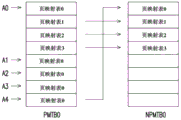
Referring to fig. 4, fig. 4 is a schematic diagram illustrating an implementation of the full-address mapping database according to an embodiment of the invention. The page mapping tables 0PMT0 to NPMTN included in the full-address mapping database are divided into a plurality of page mapping table groups, and the page mapping table groups are stored in a plurality of physical memory blocks PMTB0 to PMBTN in the flash memory, respectively. In the present embodiment, page mapping table 0 to page mapping table 3 are the same page mapping table group and stored in physical memory block PMTB0, page mapping table 4 to page mapping table 7 are the same page mapping table group and stored in physical memory block PMTB1, and page mapping table N-3 to page mapping table N are the same page mapping table group and stored in physical memory block PMTBN.
It should be noted that, in order to ensure stable data of the storage page mapping table and provide fast access, the memory storing the page mapping table may be implemented by using Single-level cell (SLC) memory cells.
Referring to fig. 5, fig. 5 is a schematic diagram illustrating an operation of integrating page mapping tables according to an embodiment of the invention. When the page mapping table needs to be updated, the updated page mapping table is written into the same physical memory block as the original page mapping table. As shown in FIG. 5, the page mapping table 0 is updated four times, so that the updated page mapping tables A1A 4 are sequentially written into the same physical memory block PMTB0 as the original page mapping table A0. After the updated page mapping table A4 is filled into the physical memory block PMTB0, the storable space of the physical memory block PMTB0 is less than a default value, and at this time, the page mapping table integration operation can be performed. Specifically, when the page mapping table integration is performed, a new replacement physical block NPMTB0 can be created. Also, the latest version of page mapping table 0a4 and page mapping tables 1-3 in physical memory block PMTB0 may be copied into replacement physical memory block NPMTB 0. After the copy operation is completed, the physical memory block PMTB0 can be released.
Through the page mapping table integrating action, the memory space of the flash memory cannot be wasted, and the updating action of the page mapping table can be continuously carried out, so that the access efficiency of the flash memory is improved.
Incidentally, the default value can be preset by an engineer and informs the memory controller to perform the corresponding checking and the integrating operation of the page mapping table through the implementation of software or hardware.
Referring to fig. 6, fig. 6 is a schematic diagram illustrating another embodiment of a management block according to the present invention. The management block 600 includes at least one empty queue 631 and an empty queue 632 (fig. 6 shows two merely exemplary examples), in addition to the page mapping table index data 610 and the logical access address 620. The blank queue 631 and the blank queue 632 can store two blank physical blocks or no valid data blocks. When a data write operation to the flash memory occurs, the memory controller receives the write data and the corresponding write logical address, and writes the write data to the empty physical memory blocks in the empty queue 631. Moreover, the memory controller can synchronously update the corresponding page mapping table according to the written logic address and the blank physical memory block.
After the data is written into the physical memory page corresponding to the empty physical memory block in the empty queue 631, the empty queue can be updated.
In another aspect, management block 600 further includes a valid count value field 640. The valid count field 640 records the number of valid pages in the corresponding physical memory block. The number of valid physical memory pages in the physical memory block can be obtained from the valid count value. When the physical banks are not used, the valid count value can provide the memory controller with a choice of which physical bank to perform the garbage collection operation. For example, when the validity count value indicates that the number of valid physical pages of a first physical bank is only one, the memory controller only needs to sort one physical page to release the first physical bank for use.
In the above embodiment, the memory controller may determine whether the number of valid memory pages is less than a predetermined value, and when the number of valid memory pages is less than the predetermined value, the memory controller may transfer the data of the valid memory pages to other physical memory blocks and release the corresponding physical memory blocks.
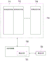
Referring to fig. 7, fig. 7 is a schematic diagram of a flash memory according to an embodiment of the invention. The flash memory 710 includes a plurality of physical memory blocks 711-71N, a memory controller 720 and a static memory 721. Each of the physical memory blocks 711-71N includes a plurality of physical memory pages. The physical memory blocks 711-71N are coupled to the memory controller 720.
The memory controller 720 is configured to perform a plurality of operations, wherein in the present embodiment, the memory controller 720 establishes a full address mapping database, wherein the full address mapping database includes a plurality of page mapping tables, each page mapping table is divided into a plurality of logical address areas, each logical address area includes a plurality of storage fields respectively corresponding to the plurality of logical page addresses, and each storage field is configured to store a physical block address and a physical page address of the corresponding logical page address mapping; moreover, the memory controller 720 establishes a management block and writes page mapping table index data into the management block; the memory controller 720 further loads one of the page mapping tables according to the page mapping table index data, and obtains the corresponding physical memory block according to the loaded page mapping table; and updating the corresponding page mapping table according to the written logical address and the blank page address.
Additionally, memory controller 720 may temporarily store the loaded page mapping table in static memory 721. The static memory 721 may be built into the memory controller 720 or external to the memory controller 720.
Details of the operations performed by the memory controller 720 are described in the foregoing embodiments and implementations, and are not repeated herein.
In summary, the present invention performs address mapping by establishing the full address mapping database and breaking the block limitation of the memory, and further completes the data access. Therefore, the access action of the flash memory can be faster, the dynamic access action can be smoothly completed, and the overall efficiency of the flash memory can be effectively improved.
Although the present invention has been described with reference to the above embodiments, it should be understood that the invention is not limited to the embodiments, and various changes and modifications can be made by one skilled in the art without departing from the spirit and scope of the invention.
Claims (14)
1. A method for accessing a flash memory, comprising:
establishing a full-address mapping database, wherein the full-address mapping database comprises a plurality of page mapping tables, each page mapping table is divided into a plurality of logical address areas, each logical address area comprises a plurality of storage fields respectively corresponding to a plurality of logical page addresses, and each storage field is used for storing a physical block address and a physical page address of a corresponding logical page address mapping;
establishing a management block, and writing page mapping table index data into the management block;
loading one of the page mapping tables according to the page mapping table index data, and acquiring a corresponding physical memory block according to the loaded page mapping table; and
performing data access operation on the physical page of the corresponding physical bank,
wherein each logical page address in each logical address region is directly mapped to the physical memory page in the corresponding physical memory block according to the storage field.
2. The method of claim 1, wherein the page mapping tables are divided into page mapping table groups, and the page mapping table groups are stored in physical memory blocks.
3. The method as claimed in claim 2, wherein when at least one of the page mapping tables in each page mapping table group is updated, the updated page mapping table is written into the corresponding physical bank.
4. The method as claimed in claim 3, further comprising when the storable space of the physical bank corresponding to each page mapping table group is less than a default value:
establishing a replacement physical memory block;
copying the latest page mapping tables in the corresponding physical memory block to the replacement physical memory block; and
and releasing the corresponding physical memory block.
5. The method of claim 1, wherein the management block records logical access addresses, and wherein the step of loading one of the page mapping tables according to the page mapping table index data and obtaining the corresponding physical memory block according to the loaded page mapping table comprises:
and obtaining the access physical address of the corresponding physical memory block through the loaded page mapping table according to the logic access address.
6. The method of claim 1, further comprising:
setting at least one blank queue in the management block, wherein the at least one blank queue stores blank physical memory blocks;
receiving write data and a corresponding write logic address, and writing the write data into a blank physical memory page of the blank physical memory block; and
and updating the corresponding page mapping table according to the written logical address and the blank physical memory block.
7. The method of claim 1, further comprising:
setting a valid count value field in the management block, wherein the valid count value field records the number of valid memory pages of the corresponding physical memory block; and
and when the number of the effective memory pages is less than a set value, transferring the data of the effective memory pages in the corresponding entity memory block to other entity memory blocks, and releasing the corresponding entity memory block.
8. A flash memory, comprising:
a plurality of physical memory blocks, each of the physical memory blocks including a plurality of physical memory pages; and
a memory controller coupled to the plurality of physical memory blocks, wherein the memory controller performs:
establishing a full-address mapping database, wherein the full-address mapping database comprises a plurality of page mapping tables, each page mapping table is divided into a plurality of logical address areas, each logical address area comprises a plurality of storage fields respectively corresponding to a plurality of logical page addresses, and each storage field is used for storing a physical block address and a physical page address of a corresponding logical page address mapping;
establishing a management block, and writing page mapping table index data into the management block;
loading one of the page mapping tables according to the page mapping table index data, and acquiring a corresponding physical memory block according to the loaded page mapping table; and
performing data access operation on the physical page of the corresponding physical bank,
wherein each logical page address in each logical address region is directly mapped to the physical memory page in the corresponding physical memory block according to the storage field.
9. The flash memory of claim 8, wherein the memory controller further distinguishes the page mapping tables into page mapping table groups, and the page mapping table groups are stored in the physical memory blocks, respectively.
10. The flash memory of claim 9, wherein when at least one of the page mapping tables in each of the page mapping table groups is updated, the updated page mapping table is written into the corresponding physical memory block
11. The flash memory of claim 10, wherein the memory controller further copies the latest page mapping tables of the corresponding physical memory block into a replacement physical memory block and releases the corresponding physical memory block.
12. The flash memory of claim 8, wherein the memory controller obtains the physical address of the corresponding physical memory block through the loaded page mapping table according to the logical access address.
13. The flash memory of claim 8, wherein the memory controller further sets at least one blank queue in the management block, wherein the at least one blank queue stores a blank physical block, receives write data and a corresponding write logical address, writes the write data to a blank physical page of the blank physical block, and updates the corresponding page mapping table according to the write logical address and the blank physical block.
14. The flash memory of claim 8, wherein the memory controller further sets a valid count field in the management block, wherein the valid count field records the number of valid pages of the corresponding physical memory block, and when the number of valid pages is smaller than a predetermined value, the memory controller forwards the data of the valid pages of the corresponding physical memory block to other physical memory blocks and releases the corresponding physical memory block.
Applications Claiming Priority (2)
| Application Number | Priority Date | Filing Date | Title |
|---|---|---|---|
| TW104144003 | 2015-12-28 | ||
| TW104144003A TWI570559B (en) | 2015-12-28 | 2015-12-28 | Flash memory and accessing method thereof |
Publications (2)
| Publication Number | Publication Date |
|---|---|
| CN106919517A CN106919517A (en) | 2017-07-04 |
| CN106919517B true CN106919517B (en) | 2021-01-26 |
Family
ID=58608261
Family Applications (1)
| Application Number | Title | Priority Date | Filing Date |
|---|---|---|---|
| CN201610093907.6A Active CN106919517B (en) | 2015-12-28 | 2016-02-19 | Flash memory and access method thereof |
Country Status (2)
| Country | Link |
|---|---|
| CN (1) | CN106919517B (en) |
| TW (1) | TWI570559B (en) |
Families Citing this family (6)
| Publication number | Priority date | Publication date | Assignee | Title |
|---|---|---|---|---|
| TWI629591B (en) * | 2017-08-30 | 2018-07-11 | 慧榮科技股份有限公司 | Method for accessing flash memory module and associated flash memory controller and electronic device |
| TWI661303B (en) * | 2017-11-13 | 2019-06-01 | 慧榮科技股份有限公司 | Method for accessing flash memory module and associated flash memory controller and electronic device |
| TWI650644B (en) * | 2018-01-05 | 2019-02-11 | 慧榮科技股份有限公司 | Method for managing flash memory module and related flash memory controller and electronic device |
| TWI761440B (en) * | 2018-01-30 | 2022-04-21 | 韓商愛思開海力士有限公司 | memory access method |
| CN109445699A (en) * | 2018-10-23 | 2019-03-08 | 江苏华存电子科技有限公司 | A kind of system of quick response blank data area read action |
| CN109446109B (en) * | 2018-10-25 | 2021-06-29 | 江苏华存电子科技有限公司 | A Method of Mixed Recording Entity Mapping Table |
Citations (4)
| Publication number | Priority date | Publication date | Assignee | Title |
|---|---|---|---|---|
| CN101727295A (en) * | 2008-10-31 | 2010-06-09 | 西安奇维测控科技有限公司 | Data writing and reading method based on virtual block flash memory address mapping |
| CN101739351A (en) * | 2008-11-06 | 2010-06-16 | 慧帝科技(深圳)有限公司 | Method for managing storage device and associated memory apparatus thereof |
| CN101911025A (en) * | 2008-01-11 | 2010-12-08 | 国际商业机器公司 | Dynamic Address Translation with Retrieval Protection |
| CN102479154A (en) * | 2010-11-30 | 2012-05-30 | 慧荣科技股份有限公司 | Method for super block management, memory device and controller thereof |
Family Cites Families (6)
| Publication number | Priority date | Publication date | Assignee | Title |
|---|---|---|---|---|
| JP3526452B2 (en) * | 2001-12-18 | 2004-05-17 | 株式会社東芝 | Disk array device and data backup method |
| TW200832440A (en) * | 2007-01-25 | 2008-08-01 | Genesys Logic Inc | Flash memory translation layer system |
| US8364931B2 (en) * | 2009-06-29 | 2013-01-29 | Mediatek Inc. | Memory system and mapping methods using a random write page mapping table |
| TWI486767B (en) * | 2012-06-22 | 2015-06-01 | Phison Electronics Corp | Data storing method, and memory controller and memory storage apparatus using the same |
| US9563551B2 (en) * | 2013-06-20 | 2017-02-07 | Silicon Motion, Inc. | Data storage device and data fetching method for flash memory |
| US9208074B2 (en) * | 2013-08-30 | 2015-12-08 | Silicon Motion, Inc. | Updating address mapping in sub-intervals in a flash memory data storage device |
-
2015
- 2015-12-28 TW TW104144003A patent/TWI570559B/en active
-
2016
- 2016-02-19 CN CN201610093907.6A patent/CN106919517B/en active Active
Patent Citations (4)
| Publication number | Priority date | Publication date | Assignee | Title |
|---|---|---|---|---|
| CN101911025A (en) * | 2008-01-11 | 2010-12-08 | 国际商业机器公司 | Dynamic Address Translation with Retrieval Protection |
| CN101727295A (en) * | 2008-10-31 | 2010-06-09 | 西安奇维测控科技有限公司 | Data writing and reading method based on virtual block flash memory address mapping |
| CN101739351A (en) * | 2008-11-06 | 2010-06-16 | 慧帝科技(深圳)有限公司 | Method for managing storage device and associated memory apparatus thereof |
| CN102479154A (en) * | 2010-11-30 | 2012-05-30 | 慧荣科技股份有限公司 | Method for super block management, memory device and controller thereof |
Also Published As
| Publication number | Publication date |
|---|---|
| TWI570559B (en) | 2017-02-11 |
| TW201723850A (en) | 2017-07-01 |
| CN106919517A (en) | 2017-07-04 |
Similar Documents
| Publication | Publication Date | Title |
|---|---|---|
| TWI741671B (en) | Memory system | |
| CN106919517B (en) | Flash memory and access method thereof | |
| US10318434B2 (en) | Optimized hopscotch multiple hash tables for efficient memory in-line deduplication application | |
| JP6778170B2 (en) | Methods and systems for reading data from persistent storage, as well as non-temporary storage media | |
| US9966152B2 (en) | Dedupe DRAM system algorithm architecture | |
| KR101465789B1 (en) | Write and merge methods in memory card systems for reducing the number of page copies | |
| US7844772B2 (en) | Device driver including a flash memory file system and method thereof and a flash memory device and method thereof | |
| US20200117368A1 (en) | Method for achieving data copying in ftl of solid state drive, system and solid state drive | |
| US10496543B2 (en) | Virtual bucket multiple hash tables for efficient memory in-line deduplication application | |
| US9436615B2 (en) | Optimistic data read | |
| US10296250B2 (en) | Method and apparatus for improving performance of sequential logging in a storage device | |
| CN105117351B (en) | To the method and device of buffering write data | |
| TW201915741A (en) | Memory system and control method for controlling non-volatile memory | |
| US12468469B2 (en) | Data processing method and system, device, storage system and medium based on access units with different data capacities | |
| CN105389264A (en) | Method and system for garbage collection in storage system | |
| CN109960471B (en) | Data storage method, device, equipment and storage medium | |
| WO2021027340A1 (en) | Storage method and apparatus for key value (kv) and storage device | |
| CN117991992A (en) | Data writing method, system, device and medium based on small partition ZNS SSD | |
| US9965398B2 (en) | Method and apparatus for simplified nameless writes using a virtual address table | |
| CN102609364A (en) | Cache exchange method | |
| CN105912279A (en) | Solid-state storage recovery system and solid-state storage recovery method | |
| CN112527692B (en) | Data storage device and non-volatile memory control method | |
| CN107632941A (en) | A kind of method for improving flash memory write performance | |
| CN118897650A (en) | Storage device for allocating unit partition area and operation method thereof | |
| US12039193B2 (en) | Apparatus, method and computer program for managing memory page updates within non-volatile memory |
Legal Events
| Date | Code | Title | Description |
|---|---|---|---|
| PB01 | Publication | ||
| PB01 | Publication | ||
| SE01 | Entry into force of request for substantive examination | ||
| SE01 | Entry into force of request for substantive examination | ||
| GR01 | Patent grant | ||
| GR01 | Patent grant |