CN106783730B - Method for forming air gap/copper interconnection - Google Patents
Method for forming air gap/copper interconnection Download PDFInfo
- Publication number
- CN106783730B CN106783730B CN201611234439.6A CN201611234439A CN106783730B CN 106783730 B CN106783730 B CN 106783730B CN 201611234439 A CN201611234439 A CN 201611234439A CN 106783730 B CN106783730 B CN 106783730B
- Authority
- CN
- China
- Prior art keywords
- copper
- oxide
- forming
- etching
- dielectric
- Prior art date
- Legal status (The legal status is an assumption and is not a legal conclusion. Google has not performed a legal analysis and makes no representation as to the accuracy of the status listed.)
- Active
Links
Images


Classifications
-
- H—ELECTRICITY
- H10—SEMICONDUCTOR DEVICES; ELECTRIC SOLID-STATE DEVICES NOT OTHERWISE PROVIDED FOR
- H10W—GENERIC PACKAGES, INTERCONNECTIONS, CONNECTORS OR OTHER CONSTRUCTIONAL DETAILS OF DEVICES COVERED BY CLASS H10
- H10W20/00—Interconnections in chips, wafers or substrates
- H10W20/01—Manufacture or treatment
- H10W20/031—Manufacture or treatment of conductive parts of the interconnections
Landscapes
- Internal Circuitry In Semiconductor Integrated Circuit Devices (AREA)
Abstract
一种形成空气隙/铜互连的方法,其包括提供一半导体衬底,先在半导体衬底上完成CMOS器件前道工艺,接着在半导体衬底上形成常规的第一介质/铜互连结构;对常规第一介质/铜互连结构在含氧的氛围中进行表面处理,在铜互连线表面形成一层铜的氧化物;采用刻蚀设备刻蚀铜互连线中间的第一介质;其中,在刻蚀第一介质过程中采用氟基气体和氧基气体进行刻蚀,铜的氧化物保护所述铜互连线没有暴露在刻蚀气体氛围中;还原铜互连线表面的铜氧化物,即使铜互连线表面的铜氧化物重新转化为金属铜;采用湿法药液去除残留光刻胶并清洗;淀积第二介质以形成空气隙/铜互连结构。

A method of forming an air gap/copper interconnect, which includes providing a semiconductor substrate, first completing a CMOS device front-end process on the semiconductor substrate, and then forming a conventional first dielectric/copper interconnect structure on the semiconductor substrate ; Surface treatment of the conventional first medium/copper interconnect structure in an oxygen-containing atmosphere to form a layer of copper oxide on the surface of the copper interconnect line; Etch the first medium in the middle of the copper interconnect line with an etching device ; wherein, in the process of etching the first medium, fluorine-based gas and oxygen-based gas are used for etching, and copper oxide protects the copper interconnection from being exposed to the etching gas atmosphere; restores the surface of the copper interconnection. Copper oxide, that is, the copper oxide on the surface of the copper interconnect is re-converted to metallic copper; the residual photoresist is removed and cleaned with a wet chemical solution; the second dielectric is deposited to form an air gap/copper interconnect structure.
Description
技术领域technical field
本发明涉及半导体加工制造领域,尤其是,涉及一种形成空气隙/铜互连的方法。The present invention relates to the field of semiconductor processing and manufacturing, and more particularly, to a method for forming air gap/copper interconnects.
背景技术Background technique
晶体管随着摩尔定律不断发展,特征线宽越来越小,集成密度越来越高,性能越来越强大。对于互补金属氧化物半导体(Complementary Metal Oxide Semiconductor,简称CMOS)晶体管而言,速度是表征其性能的重要指标。With the continuous development of Moore's Law, the characteristic line width of transistors is getting smaller and smaller, the integration density is getting higher and higher, and the performance is getting stronger and stronger. For Complementary Metal Oxide Semiconductor (Complementary Metal Oxide Semiconductor, CMOS for short) transistors, speed is an important indicator to characterize its performance.
本领域技术人员清楚,CMOS的速度与CMOS的延迟相关,CMOS的延迟可以细分为前道器件的延迟和后道互连线的延迟;并且,随着半导体工艺尺寸减少,后道互连线的CMOS延迟的影响变得越来越大,在先进工艺中已经成为最主要的延迟。后道互连线的延迟主要是由互连导线的电阻R和互连导线间电容C(即RC)决定的。It is clear to those skilled in the art that the speed of CMOS is related to the delay of CMOS, and the delay of CMOS can be subdivided into the delay of the front-end device and the delay of the back-end interconnect; The impact of CMOS delays has become larger and larger, and has become the most dominant delay in advanced processes. The delay of the rear interconnection line is mainly determined by the resistance R of the interconnection wire and the capacitance C (ie RC) between the interconnection wires.
为了降低后道互连线RC延迟,集成电路制造商一直在想办法降低互连导线电阻和互连导线间电容,如采用电阻率更低的铜导线代替铝导线,采用介电常数更低的low-k介质代替二氧化硅介质。In order to reduce the RC delay of the back-end interconnects, integrated circuit manufacturers have been looking for ways to reduce the interconnection wire resistance and the capacitance between interconnection wires, such as using copper wires with lower resistivity instead of aluminum wires, using lower dielectric constant. low-k media instead of silica media.
对于后者,已经经过了数个技术带的技术更新,互连导线间介质从SiO2→F dopedSiO2(FSG)→BD I→BD II→BD III的改进过程中,互连导线间介质的介电常数在持续降低,以此满足减小后道互连线RC的需求。For the latter, it has undergone several technical updates in technology bands. During the improvement process of the inter-conductor dielectric from SiO 2 →F dopedSiO 2 (FSG)→BD I→BD II→BD III, the The dielectric constant continues to decrease in order to meet the need to reduce the RC of the rear interconnect.
众所周知,真空的相对介电常数为1,空气的相对介电常数也约为1,其为最常见的最小相对介电常数的介质。因此,采用空气部分代替互连线之间的传统介质也随之被提出,这就是空气隙/铜互连结构技术。As we all know, the relative permittivity of vacuum is 1, and the relative permittivity of air is also about 1, which is the most common medium with the smallest relative permittivity. Therefore, the use of air parts to replace the traditional medium between interconnect lines is also proposed, which is the air gap/copper interconnect structure technology.
空气隙的形成方法大致可以分成以下两大类:The formation methods of air gaps can be roughly divided into the following two categories:
第一类,先采用传统的工艺形成正常的介质/铜互连结构,然后通过刻蚀工艺去除铜互连线之间的介质,最后通过化学气相淀积工艺形成空气隙;In the first type, a normal dielectric/copper interconnect structure is formed by a traditional process, then the dielectric between the copper interconnect lines is removed by an etching process, and finally an air gap is formed by a chemical vapor deposition process;
第二类,采用牺牲层,如thermal degradable polymer,在完成铜互连结构后去除牺牲层,形成空气隙。The second type uses a sacrificial layer, such as thermal degradable polymer, to remove the sacrificial layer after completing the copper interconnect structure to form an air gap.
目前对于大多数集成电路生产企业而言,第一类方法的工艺兼容性更高,因此更容易被接收。下面通过附图1-3,简述一下现有技术中采用第一类方法制备空气隙/铜互连结构的工艺方法。Currently, for most IC manufacturers, the first type of approach is more process compatible and therefore easier to accept. The following briefly describes a process method for preparing an air gap/copper interconnect structure using the first type of method in the prior art with reference to accompanying drawings 1-3.
步骤S01:先在半导体衬底101上形成传统的第一介质102/铜104互连结构,该部分工艺与现有CMOS工艺完全一样,没有额外的工艺成本和风险(如图1所示),在此不再赘述;Step S01 : firstly forming a traditional first dielectric 102/
步骤S02:除去铜互连导线之间的第一介质,如采用介质刻蚀工艺去除部分第一介质得到如图2所示结构;然而,在刻蚀过程中会使得铜104的表面被氧化,得到一定厚度的铜氧化物105;Step S02 : removing the first dielectric between the copper interconnecting wires. For example, a dielectric etching process is used to remove part of the first dielectric to obtain the structure shown in FIG. 2 ; however, the surface of the
步骤S03:采用后道清洗药液去除残留的光刻胶并清洗硅片;在清洗的过程中,由于铜氧化物105很容易被后道清洗药液腐蚀,且后道清洗药液不腐蚀阻挡层103,因此,最后留下阻挡层“耳朵”103’,如图3所示。Step S03: use the subsequent cleaning liquid to remove the remaining photoresist and clean the silicon wafer; during the cleaning process, the
由于阻挡层“耳朵”103’的存在,该结构在后续工艺及器件性能上带来一系列负面影响,例如,在采用化学气相淀积介质时,会出现:Due to the existence of the "ear" 103' of the barrier layer, this structure brings a series of negative effects on the subsequent process and device performance. For example, when chemical vapor deposition medium is used, there will be:
①、该阻挡层“耳朵”103’周围的台阶覆盖性能变差;①, the step coverage performance around the "ear" 103' of the barrier layer becomes poor;
②、该阻挡层“耳朵”103’的机械强度差而导致坍塌;②, the mechanical strength of the barrier "ear" 103' is poor, resulting in collapse;
③、该阻挡层“耳朵”103’尖端电场强度发生改变等,直接导致CMOS晶体管性能恶化等。③. The electric field intensity at the tip of the barrier "ear" 103' changes, etc., which directly leads to the deterioration of the performance of the CMOS transistor.
发明内容SUMMARY OF THE INVENTION
针对现有技术存在的不足,本发明的目的在于提供一种形成空气隙/铜互连的方法,以解决现有技术因为存在阻挡层“耳朵”而导致的晶体管性能恶化的问题,其避免了阻挡层“耳朵”的产生,不仅有利于化学气相淀积工艺淀积介质并形成空气隙,且提高了晶体管性能。In view of the deficiencies in the prior art, the purpose of the present invention is to provide a method for forming an air gap/copper interconnect, so as to solve the problem of the deterioration of transistor performance caused by the existence of barrier layer "ears" in the prior art, which avoids The creation of the "ears" of the barrier layer is not only conducive to the chemical vapor deposition process for depositing the medium and forming the air gap, but also improving the performance of the transistor.
为实现上述目的,本发明的技术方案如下:For achieving the above object, technical scheme of the present invention is as follows:
一种形成空气隙/铜互连的方法,其特征在于,包括:A method of forming an air gap/copper interconnect, comprising:
步骤S1:提供一半导体衬底,先在半导体衬底上完成CMOS器件前道工艺,接着继续形成后道铜互连线,即在所述半导体衬底上形成常规的第一介质/铜互连结构;Step S1: Provide a semiconductor substrate, first complete the front-end process of the CMOS device on the semiconductor substrate, and then continue to form the subsequent copper interconnect lines, that is, form a conventional first dielectric/copper interconnect on the semiconductor substrate structure;
步骤S2:对所述常规第一介质/铜互连结构在含氧的氛围中进行表面处理,在所述铜互连线表面形成一层铜的氧化物;Step S2: performing surface treatment on the conventional first dielectric/copper interconnect structure in an oxygen-containing atmosphere to form a layer of copper oxide on the surface of the copper interconnect wire;
步骤S3:采用刻蚀设备刻蚀所述铜互连线中间的第一介质;其中,在刻蚀第一介质过程中采用氟基气体和氧基气体进行刻蚀,所述铜的氧化物保护所述铜互连线没有暴露在刻蚀气体氛围中;Step S3: Etching the first medium in the middle of the copper interconnect lines by using an etching device; wherein, in the process of etching the first medium, fluorine-based gas and oxygen-based gas are used for etching, and the copper oxide protects the copper interconnects are not exposed to an etching gas atmosphere;
步骤S4:还原所述铜互连线表面的铜氧化物,即使所述铜互连线表面的铜氧化物重新转化为金属铜;Step S4: reducing the copper oxide on the surface of the copper interconnection, even if the copper oxide on the surface of the copper interconnection is re-converted into metallic copper;
步骤S5:采用湿法药液去除残留光刻胶并清洗;Step S5: removing the residual photoresist and cleaning with a wet chemical solution;
步骤S6:淀积第二介质,形成所述空气隙/铜互连结构。Step S6: depositing a second medium to form the air gap/copper interconnect structure.
优选地,所述步骤S1具体包括:Preferably, the step S1 specifically includes:
步骤S11:在半导体衬底上淀积第一介质层;Step S11: depositing a first dielectric layer on the semiconductor substrate;
步骤S12:采用光刻刻蚀工艺在所述第一介质层中形成大马士革槽或者双大马士革孔槽;Step S12: using a photolithography etching process to form a Damascus groove or a double Damascus hole groove in the first dielectric layer;
步骤S13:分别淀积阻挡层材料和铜互连材料;Step S13: depositing the barrier layer material and the copper interconnect material respectively;
步骤S14:经过研磨工艺形成阻挡层和铜互连层,即在所述半导体衬底上形成常规的第一介质/铜互连结构。Step S14 : forming a barrier layer and a copper interconnection layer through a grinding process, that is, forming a conventional first dielectric/copper interconnection structure on the semiconductor substrate.
优选地,所述常规第一介质/铜互连结构中的第一介质材料为氧化硅、氟掺杂的氧化硅、碳掺杂的氧化硅、氮化硅、氮掺杂的碳化硅中的一种或者多种。Preferably, the first dielectric material in the conventional first dielectric/copper interconnect structure is one of silicon oxide, fluorine-doped silicon oxide, carbon-doped silicon oxide, silicon nitride, and nitrogen-doped silicon carbide. one or more.
优选地,所述介质用氮掺杂的碳化硅/碳掺杂的氧化硅/氧化硅多层叠层结构。Preferably, the dielectric is a nitrogen-doped silicon carbide/carbon-doped silicon oxide/silicon oxide multilayer structure.
优选地,在步骤S2中,在所述铜互连线表面形成的一层铜的氧化物的厚度可控且厚度均匀,所述铜的氧化物的厚度为30~300埃。Preferably, in step S2, the thickness of a layer of copper oxide formed on the surface of the copper interconnection line is controllable and uniform, and the thickness of the copper oxide is 30-300 angstroms.
优选地,在步骤S3中,采用CF4/O2混合气体刻蚀所述第一介质层。Preferably, in step S3, CF4/O2 mixed gas is used to etch the first dielectric layer.
优选地,在步骤S4中,所述还原铜导线表面的铜氧化物副产品所采用的还原性物质为氢气和/或氨气气体或者氢气和/或氨气的等离子体。Preferably, in step S4, the reducing substance used for reducing the copper oxide by-product on the surface of the copper wire is hydrogen gas and/or ammonia gas or plasma of hydrogen gas and/or ammonia gas.
优选地,在步骤S5中,所述去除残留光刻胶的后道湿法药液选择对残留光刻胶的腐蚀速率大于对所述铜的氧化物的腐蚀速率。Preferably, in step S5, the etching rate of the residual photoresist is selected to be greater than the etching rate of the copper oxide by the wet chemical solution for removing the residual photoresist.
优选地,在步骤S6中,采用化学气相淀积方法或采用等离子体增强化学气相淀积设备沉积所述第二介质层。Preferably, in step S6, the second dielectric layer is deposited by a chemical vapor deposition method or a plasma enhanced chemical vapor deposition device.
优选地,所述第二介质层为氧化硅、氟掺杂的氧化硅、碳掺杂的氧化硅、氮化硅、氮掺杂的碳化硅中的一种或者多种。Preferably, the second dielectric layer is one or more of silicon oxide, fluorine-doped silicon oxide, carbon-doped silicon oxide, silicon nitride, and nitrogen-doped silicon carbide.
从上述技术方案可以看出,在本发明提供的一种形成空气隙/铜互连的方法中,其先通过表面处理技术在常规介质/铜互连结构中的铜表面形成一层厚度均匀的铜的氧化物,然后在介质刻蚀后通过采用还原性物质将铜表面的铜的氧化物重新转化为金属铜,最后再采用后道湿法药液去除残留光刻胶并清洗,避免了现有技术中由于后道湿法药液腐蚀铜的氧化物而造成的阻挡层“耳朵”结构,有利于后续介质的淀积和空气隙的形成,提高晶体管的性能。It can be seen from the above technical solutions that in the method for forming an air gap/copper interconnect provided by the present invention, a layer of uniform thickness is first formed on the copper surface of the conventional dielectric/copper interconnect structure by surface treatment technology. Copper oxide, and then after dielectric etching, the copper oxide on the copper surface is re-converted into metal copper by using a reducing substance, and finally the residual photoresist is removed and cleaned by the subsequent wet chemical solution, which avoids the occurrence of current problems. In the prior art, the "ear" structure of the barrier layer caused by the corrosion of copper oxide by the subsequent wet chemical solution is beneficial to the deposition of the subsequent medium and the formation of air gaps, and improves the performance of the transistor.
附图说明Description of drawings
图1所示为现有技术中在半导体衬底上形成传统的第一介质/铜互连结构的典型示意图FIG. 1 shows a typical schematic diagram of forming a conventional first dielectric/copper interconnect structure on a semiconductor substrate in the prior art
图2所示为现有技术中完成第一介质/铜互连结构除去铜互连导线之间第一介质后的结构示意图FIG. 2 is a schematic diagram showing the structure of the prior art after the first dielectric/copper interconnect structure is completed and the first dielectric between the copper interconnect wires is removed.
图3所示为现有技术中完成后道清洗步骤后留下阻挡层“耳朵”的结构示意图Figure 3 is a schematic diagram showing the structure of the barrier layer "ear" left after the post-cleaning step in the prior art
图4为本发明所提出的一种形成空气隙/铜互连的方法流程示意图FIG. 4 is a schematic flowchart of a method for forming an air gap/copper interconnect according to the present invention
图5为本发明形成空气隙/铜互连的方法一实施例中完成步骤S1后所形成的剖面示意图FIG. 5 is a schematic cross-sectional view of a method for forming an air gap/copper interconnect according to an embodiment of the present invention after step S1 is completed.
图6为本发明形成空气隙/铜互连的方法一实施例中完成步骤S2后所形成的剖面示意图6 is a schematic cross-sectional view of a method for forming an air gap/copper interconnect according to an embodiment of the present invention after step S2 is completed
图7为本发明形成空气隙/铜互连的方法一实施例中完成步骤S3后所形成的剖面示意图7 is a schematic cross-sectional view of the method for forming an air gap/copper interconnect according to an embodiment of the present invention after step S3 is completed
图8为本发明形成空气隙/铜互连的方法一实施例中完成步骤S3后所形成的剖面示意图8 is a schematic cross-sectional view of the method for forming an air gap/copper interconnect according to an embodiment of the present invention after step S3 is completed
具体实施方式Detailed ways
下面结合附图对本发明的具体实施方式进行详细的说明。应理解的是本发明能够在不同的示例上具有各种的变化,其皆不脱离本发明的范围,且其中的说明及图示在本质上当做说明之用,而非用以限制本发明。The specific embodiments of the present invention will be described in detail below with reference to the accompanying drawings. It should be understood that the present invention is capable of various changes in different examples without departing from the scope of the present invention, and the descriptions and drawings therein are for illustrative purposes in nature, rather than limiting the present invention.
现结合附图4-8,通过具体实施例对本发明的一种形成空气隙/铜互连的方法作进一步详细说明。需说明的是,附图均采用非常简化的形式且均使用非精准的比例,仅用以方便、明晰地辅助说明本发明实施例的目的。Now, a method for forming an air gap/copper interconnection of the present invention will be further described in detail through specific embodiments with reference to the accompanying drawings 4-8. It should be noted that, the accompanying drawings are all in a very simplified form and in inaccurate scales, and are only used to facilitate and clearly assist the purpose of explaining the embodiments of the present invention.
请参阅图4,如图所示为本发明的一种形成空气隙/铜互连的方法一个较佳实施例的流程示意图。在本实施例中,一种形成空气隙/铜互连的方法包括如下步骤:Please refer to FIG. 4 , which is a schematic flowchart of a preferred embodiment of a method for forming an air gap/copper interconnect according to the present invention. In this embodiment, a method for forming an air gap/copper interconnect includes the following steps:
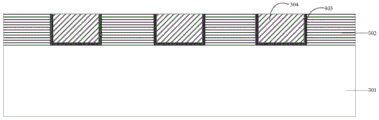
步骤S01:提供一半导体衬底,先在半导体衬底上完成CMOS器件前道工艺,接着继续形成后道铜互连线,即在所述半导体衬底上形成常规的第一介质/铜互连结构。具体的,请参阅图5,图5为本发明形成空气隙/铜互连的方法一实施例中完成步骤S1后所形成的剖面示意图。Step S01 : providing a semiconductor substrate, first completing the front-end process of the CMOS device on the semiconductor substrate, and then continuing to form the subsequent copper interconnect lines, that is, forming a conventional first dielectric/copper interconnect on the semiconductor substrate structure. Specifically, please refer to FIG. 5 . FIG. 5 is a schematic cross-sectional view formed after step S1 is completed in an embodiment of the method for forming an air gap/copper interconnect according to the present invention.
如图所示,本步骤先在衬底硅片301上完成CMOS器件前道工艺,接着继续形成后道互连线,形成常规的介质302/铜互连304结构,其中,标号303为阻挡层。As shown in the figure, this step first completes the front-end process of the CMOS device on the
下面通过一12英寸的晶圆硅片作为一可选的实施方式,对采用公知的CMOS工艺,在硅片上形成常规的前道CMOS器件结构,接着采用铜互连工艺形成互连线的具体步骤进行说明。Hereinafter, a 12-inch silicon wafer is used as an optional implementation manner to form a conventional front-channel CMOS device structure on the silicon wafer by using a well-known CMOS process, and then use a copper interconnect process to form the specific details of the interconnect lines. steps are explained.
具体而言,在该实施例中,步骤S1可以包括如下步骤:Specifically, in this embodiment, step S1 may include the following steps:
步骤S11:在半导体衬底301上淀积第一介质层302;Step S11: depositing a first
步骤S12:采用光刻刻蚀工艺在第一介质层302中形成大马士革槽或者双大马士革孔槽;Step S12: forming a Damascus groove or a double Damascus hole groove in the
步骤S13:分别淀积阻挡层材料和铜互连材料;Step S13: depositing the barrier layer material and the copper interconnect material respectively;
步骤S14:经过研磨工艺形成阻挡层303和铜互连层304,即在半导体衬底上形成常规的第一介质/铜互连结构。Step S14: The
较佳地,所淀积的常规第一介质302可以为氧化硅、氟掺杂的氧化硅、碳掺杂的氧化硅、氮化硅、氮掺杂的碳化硅中的一种或者多种,在本发明的实施例中,第一介质302采用氮掺杂的碳化硅/碳掺杂的氧化硅/氧化硅多层叠层结构。Preferably, the deposited conventional
步骤S2:对常规第一介质/铜互连结构在含氧的氛围中进行表面处理,在铜互连线表面形成一层铜的氧化物。请参阅图6,图6为本发明形成空气隙/铜互连的方法一实施例中完成步骤S2后所形成的剖面示意图。Step S2: performing surface treatment on the conventional first dielectric/copper interconnect structure in an oxygen-containing atmosphere to form a layer of copper oxide on the surface of the copper interconnect wire. Please refer to FIG. 6 . FIG. 6 is a schematic cross-sectional view of a method for forming an air gap/copper interconnect according to an embodiment of the present invention after step S2 is completed.
如图6所示,在本实施例中,将常规第一介质/铜互连结构置于含氧的氛围中进行表面处理,在互连金属铜304的表面形成一层厚度可控且厚度均匀的铜的氧化物305,较佳地,铜的氧化物的厚度可以为30~300埃。As shown in FIG. 6 , in this embodiment, the conventional first dielectric/copper interconnect structure is placed in an oxygen-containing atmosphere for surface treatment, and a layer of controllable and uniform thickness is formed on the surface of the
例如,在本实施例中,将常规介质/铜互连结构置于等离子体化学气相淀积设备中,采用氧等离子进行处理,在铜互连304表面得到100埃厚度的铜的氧化物。For example, in this embodiment, a conventional dielectric/copper interconnect structure is placed in a plasma chemical vapor deposition apparatus, and treated with oxygen plasma to obtain a copper oxide with a thickness of 100 angstroms on the surface of the
该铜的氧化物305不易被含氟的气体刻蚀,刻蚀气体中的氧也不易再继续氧化互连金属铜,因此该铜的氧化物充当后续工艺中的保护层。The
步骤S3:采用刻蚀设备刻蚀所述铜互连线中间的第一介质;其中,在刻蚀第一介质过程中采用氟基气体和氧基气体进行刻蚀,铜的氧化物保护铜互连线没有暴露在刻蚀气体氛围中。请参阅图7,图7为本发明形成空气隙/铜互连的方法一实施例中完成步骤S3后所形成的剖面示意图。Step S3: Etching the first medium in the middle of the copper interconnect lines by using an etching device; wherein, in the process of etching the first medium, fluorine-based gas and oxygen-based gas are used for etching, and copper oxides protect the copper interconnects. The wires are not exposed to the etching gas atmosphere. Please refer to FIG. 7 . FIG. 7 is a schematic cross-sectional view of a method for forming an air gap/copper interconnect according to an embodiment of the present invention after step S3 is completed.
具体的,如图7所示,在本实施例中,可以采用光刻、刻蚀工艺去除铜互连线304之间的第一介质302。在刻蚀第一介质302过程中采用氟基气体和氧基气体进行刻蚀,但由于铜互连线304表面有一层铜的氧化物305作为保护层,因此,只会刻蚀掉需要去除的第一介质302。Specifically, as shown in FIG. 7 , in this embodiment, photolithography and etching processes may be used to remove the
在本实施例中,可以采用CF4/O2混合气体刻蚀第一介质层302,由于铜互连304表面有一层铜的氧化物305,可以阻止金属铜304被氧化,因此,铜的氧化物305起到刻蚀保护层的作用。In this embodiment, the
步骤S4:还原铜互连线表面的铜氧化物,即使铜互连线表面的铜氧化物重新转化为金属铜。Step S4 : reducing the copper oxide on the surface of the copper interconnection, even if the copper oxide on the surface of the copper interconnection is re-converted to metallic copper.
具体的,请参阅图8,在本实施例中,可以采用还原性物质将铜表面的铜的氧化物305重新转化为金属铜306,较佳地,还原性物质为氢气、氨气气体或者氢气、氨气的等离子体。Specifically, please refer to FIG. 8 . In this embodiment, the
在本实施例中,在刻蚀腔体中,采用氢等离子还原铜的氧化物305,将其重新转化为金属铜,由于铜的氧化物305厚度已知且厚度均匀,因此便于设置还原工艺条件,提高工艺均匀性。In this embodiment, in the etching chamber, hydrogen plasma is used to reduce the
步骤S5:采用湿法药液去除残留光刻胶并清洗。Step S5 : removing the residual photoresist with a wet chemical solution and cleaning.
具体的,采用后道湿法药液将刻蚀残留的光刻胶去除并将硅片表面清洗干净,且后道湿法药液对残留的光刻胶的腐蚀速率远远大于对金属铜的腐蚀速率,因此,不会再形成阻挡层“耳朵”。Specifically, the photoresist remaining after etching is removed and the surface of the silicon wafer is cleaned by the subsequent wet chemical solution, and the corrosion rate of the remaining photoresist by the subsequent wet chemical solution is much higher than that of metal copper. Corrosion rate, therefore, no more barrier "ears" are formed.
步骤S6:淀积第二介质材料,形成所述空气隙/铜互连结构。Step S6: depositing a second dielectric material to form the air gap/copper interconnect structure.
具体的,可以采用化学气相淀积方法沉积第二介质层,形成空气隙/铜互连结构。第二介质层可以为氧化硅、氟掺杂的氧化硅、碳掺杂的氧化硅、氮化硅、氮掺杂的碳化硅中的一种或者多种,所形成的空气隙位于铜互连线之间。本实施例中,可以采用等离子体增强化学气相淀积设备依此沉积掺氮的碳化硅和掺碳的氧化硅,由于铜互连304之间的槽的深宽比较高,因此,在沉积第二介质材料时会自动在金属铜互连之间形成空气隙,形成空气隙/铜互连结构。Specifically, a chemical vapor deposition method can be used to deposit the second dielectric layer to form an air gap/copper interconnect structure. The second dielectric layer can be one or more of silicon oxide, fluorine-doped silicon oxide, carbon-doped silicon oxide, silicon nitride, and nitrogen-doped silicon carbide, and the formed air gap is located in the copper interconnection between the lines. In this embodiment, plasma-enhanced chemical vapor deposition equipment can be used to deposit nitrogen-doped silicon carbide and carbon-doped silicon oxide accordingly. When two dielectric materials are used, an air gap will be automatically formed between the metal copper interconnects, forming an air gap/copper interconnect structure.
综上所述,在本发明提供的一种形成空气隙/铜互连的方法中,通过先采用表面处理技术在常规介质/铜互连结构中的铜表面形成一层厚度可控且厚度均匀的铜的氧化物,然后在介质刻蚀后通过采用还原性物质将铜表面的铜的氧化物重新转化为金属铜,大大降低后道湿法药液的腐蚀速率,提高了工艺可控性及一致性,避免形成阻挡层“耳朵”结构,且能有效提高晶体管器件性能。To sum up, in a method for forming an air gap/copper interconnect provided by the present invention, a layer with a controllable and uniform thickness is formed on the copper surface of a conventional dielectric/copper interconnect structure by first using a surface treatment technology. Then, after dielectric etching, the copper oxide on the copper surface is re-converted into metallic copper by using a reducing substance, which greatly reduces the corrosion rate of the subsequent wet chemical solution, and improves the process controllability and efficiency. Consistency, avoid the formation of barrier layer "ear" structure, and can effectively improve the performance of transistor devices.
以上的仅为本发明的实施例,实施例并非用以限制本发明的专利保护范围,因此凡是运用本发明的说明书及附图内容所作的等同结构变化,同理均应包含在本发明的保护范围内。The above are only the embodiments of the present invention, and the embodiments are not intended to limit the scope of patent protection of the present invention. Therefore, any equivalent structural changes made by using the contents of the description and drawings of the present invention should be included in the protection of the present invention. within the range.
Claims (10)
Priority Applications (1)
| Application Number | Priority Date | Filing Date | Title |
|---|---|---|---|
| CN201611234439.6A CN106783730B (en) | 2016-12-28 | 2016-12-28 | Method for forming air gap/copper interconnection |
Applications Claiming Priority (1)
| Application Number | Priority Date | Filing Date | Title |
|---|---|---|---|
| CN201611234439.6A CN106783730B (en) | 2016-12-28 | 2016-12-28 | Method for forming air gap/copper interconnection |
Publications (2)
| Publication Number | Publication Date |
|---|---|
| CN106783730A CN106783730A (en) | 2017-05-31 |
| CN106783730B true CN106783730B (en) | 2020-09-04 |
Family
ID=58924469
Family Applications (1)
| Application Number | Title | Priority Date | Filing Date |
|---|---|---|---|
| CN201611234439.6A Active CN106783730B (en) | 2016-12-28 | 2016-12-28 | Method for forming air gap/copper interconnection |
Country Status (1)
| Country | Link |
|---|---|
| CN (1) | CN106783730B (en) |
Family Cites Families (9)
| Publication number | Priority date | Publication date | Assignee | Title |
|---|---|---|---|---|
| JPH04273437A (en) * | 1991-02-28 | 1992-09-29 | Sony Corp | Dry etching method |
| JP3137087B2 (en) * | 1998-08-31 | 2001-02-19 | 日本電気株式会社 | Method for manufacturing semiconductor device |
| TWI227043B (en) * | 2000-09-01 | 2005-01-21 | Koninkl Philips Electronics Nv | Method of manufacturing a semiconductor device |
| US7371427B2 (en) * | 2003-05-20 | 2008-05-13 | Applied Materials, Inc. | Reduction of hillocks prior to dielectric barrier deposition in Cu damascene |
| CN101123215A (en) * | 2006-08-11 | 2008-02-13 | 联华电子股份有限公司 | copper damascene process |
| JP2009194286A (en) * | 2008-02-18 | 2009-08-27 | Panasonic Corp | Semiconductor device and manufacturing method thereof |
| JP5143769B2 (en) * | 2008-03-12 | 2013-02-13 | 東京エレクトロン株式会社 | Semiconductor device and manufacturing method thereof |
| CN102969273A (en) * | 2012-10-25 | 2013-03-13 | 上海集成电路研发中心有限公司 | Forming method of copper Damascus interconnection structure with air gaps |
| CN103633021B (en) * | 2013-12-02 | 2015-12-30 | 上海华力微电子有限公司 | A kind of method preparing air gap copper interconnection structure |
-
2016
- 2016-12-28 CN CN201611234439.6A patent/CN106783730B/en active Active
Also Published As
| Publication number | Publication date |
|---|---|
| CN106783730A (en) | 2017-05-31 |
Similar Documents
| Publication | Publication Date | Title |
|---|---|---|
| CN100501937C (en) | Method of forming a low k dielectric in a semiconductor manufacturing process | |
| CN101989570A (en) | Forming method of contact hole structure | |
| CN101419923B (en) | Manufacturing method of lead pad | |
| CN103378052A (en) | Semiconductor devices, methods of manufacture thereof, and methods of forming conductive features | |
| CN102237296A (en) | Through hole etching method | |
| CN108305827A (en) | A method of removal etching procedure residual polyalcohol | |
| CN1327494C (en) | Manufacturing method of low dielectric constant layer | |
| US20160358811A1 (en) | Interconnect structure | |
| CN102082115A (en) | Aluminum interconnection structure and method for forming aluminum interconnection structure | |
| CN108598259A (en) | A kind of preparation method of film resistor | |
| CN110504211A (en) | Improve the process of the mound shape bump defects of top copper interconnection layer | |
| CN104900579B (en) | The forming method of semiconductor devices | |
| CN102543843A (en) | Manufacturing method of interconnection structure | |
| CN106783730B (en) | Method for forming air gap/copper interconnection | |
| CN106847740B (en) | A kind of process method of forming air gap/copper interconnect | |
| CN104282618A (en) | Method for forming semiconductor device | |
| CN104347489A (en) | Forming method of conductive plug | |
| CN106611743A (en) | Method of manufacturing air gap/copper interconnection structure | |
| CN108376676B (en) | A metal interconnect structure with a porous dielectric layer | |
| CN110148584A (en) | Method of forming an air gap | |
| CN105609438B (en) | Bonding pad forming method | |
| CN104167388B (en) | A kind of forming method of subsequent interconnection technique hollow air-gap | |
| CN107359115A (en) | The forming method of pad | |
| CN103915371A (en) | Method for forming through hole and trench | |
| CN104112699A (en) | Method for eliminating bump effect in semiconductor structure |
Legal Events
| Date | Code | Title | Description |
|---|---|---|---|
| PB01 | Publication | ||
| PB01 | Publication | ||
| SE01 | Entry into force of request for substantive examination | ||
| SE01 | Entry into force of request for substantive examination | ||
| GR01 | Patent grant | ||
| GR01 | Patent grant | ||
| TR01 | Transfer of patent right |
Effective date of registration: 20210225 Address after: No. 497, Gauss Road, Zhangjiang, Pudong New Area, Shanghai, 201210 Patentee after: SHANGHAI IC R&D CENTER Co.,Ltd. Patentee after: Semiconductor Manufacturing International (Shanghai) Corp. Address before: 201210 No.497 Gaosi Road, Zhangjiang, Pudong New Area, Shanghai Patentee before: SHANGHAI IC R&D CENTER Co.,Ltd. |
|
| TR01 | Transfer of patent right |