This application claims priority to U.S. provisional patent application No. 61/989,799, filed 5/7/2014 and U.S. provisional patent application No. 62/072,992, filed 10/30/2014, each of which is incorporated herein by reference in its entirety.
Detailed Description
Wireless power transfer systems that rely on an oscillating magnetic field between two coupled resonators may be efficient, non-radiative, and safe. The non-magnetic and/or non-metallic objects inserted between the resonators may not substantially interact with the magnetic field used for wireless energy transfer. In some embodiments, a user of the wireless power transfer system may wish to detect the presence of these "alien materials," and may wish to control, turn down, shut down, alert, etc. the wireless power transfer system. Metal and/or other objects inserted between the resonators may interact with the magnetic field of the wireless power transfer system in a manner such that these metal and/or other objects disturb the wireless energy transfer and/or generate heat substantially. In some embodiments, a user of the wireless power transfer system may wish to detect the presence of these "alien materials," and may wish to control, turn down, shut down, alert, etc. the wireless power transfer system. In some embodiments, a user may detect heating of the wireless power transfer system and control, turn down, shut down, set alarms for the system for safe operation. For example, techniques for detecting the presence of Foreign objects or detecting heating of a Wireless power Transfer System for Wireless power Transfer are described in commonly owned U.S. patent application 13/608,956 entitled "article Object Detection in Wireless Energy Transfer Systems," filed on 9/2011, U.S. provisional application 61/532,785 entitled "article Object Detection in Wireless Energy Transfer Systems," filed on 9/2011, U.S. patent application 12/899,281 entitled "Vehicle Charger Safety Systems and methods," filed on 10/6/2010, and U.S. patent application 12/567,716 entitled "Wireless Energy Transfer Systems," filed on 9/25/2009, each of which is incorporated herein by reference.
Foreign Objects (FODs) in the vicinity of a wireless power transfer system may be harmless and/or may interact with fields used for energy transfer in a harmless manner. Examples of harmless FODs may include dirt, sand, leaves, branches, snow, grease, oil, water, and other substances that may not significantly interact with low frequency magnetic fields. In an embodiment, the FOD may comprise an object that is able to interact with the field used for wireless power transfer in a non-harmful way, but this may be limited to an area very close to the resonator of the wireless transfer system due to perceived danger or from a prudent advantage. A common example of this type of FOD is a cat that may wish to sleep between resonators and/or resonator coils of a wireless vehicle charging system. While unlikely, some humans, particularly children, may perceive the possibility of being between resonators themselves in high power systems where human exposure effects may exceed certain exposure guidelines and regulations. In some cases, humans, animals, organic materials, and the like may be a FOD in a wireless power transfer system. In some embodiments, the detection of living objects such as cats and humans may be referred to as live detection (LOD). In embodiments, some FODs may interact with magnetic fields in a manner that may disturb the characteristics of the resonators used for energy transfer, may block or reduce the magnetic fields used for energy transfer, or may create a fire and/or fire hazard. In some applications, special precautions may be required to avoid combustible metal objects becoming hot enough to ignite during high power charging. Some metal objects may heat up and have sufficient heat capacity to cause burns or discomfort to people who may pick them up while they are still hot. Examples include tools, coils, metal sheets, soda cans, steel wool, packaging for food (chewing gum, hamburgers, etc.), cigarette packaging with metal foil, and the like.
Accordingly, there is a need for methods and designs for detecting or mitigating the effects of FOD in the vicinity of a wireless power transfer system.
Methods of mitigating FOD risk can be divided into passive mitigation techniques and active mitigation techniques. Passive mitigation techniques can be used to prevent FODs from entering or remaining in areas of high electromagnetic fields (e.g., magnetic fields, electric fields). Passive mitigation techniques can reduce the likelihood of dangerous interactions of the FOD with electromagnetic fields. Active mitigation techniques can be used to detect and react to the presence of FOD.
In the present invention, "wireless energy transfer" from one coil (e.g., a resonator coil) to another coil (e.g., another resonator coil) refers to transferring energy to perform useful work (e.g., mechanical work), such as powering an electronic device, a vehicle, lighting a light bulb, or charging a battery, etc. Similarly, "wireless power transfer" from one coil (e.g., a resonator coil) to another resonator (e.g., another resonator coil) refers to transferring power to perform useful work (e.g., mechanical work), such as powering an electronic device, a vehicle, lighting a light bulb, or charging a battery, etc. Wireless energy transfer and wireless power transfer both refer to the transfer of energy (or equivalently, the transmission of energy) to provide operating power that would otherwise be provided through a connection to an electrical power source, such as a connection to a mains voltage source, etc. Thus, with the above understanding, the expressions "wireless energy transfer" and "wireless power transfer" are used interchangeably in the present invention. It should also be understood that "wireless power transfer" and "wireless energy transfer" may accompany the transfer of information, that is, information may be transferred via electromagnetic signals along with energy or power to perform useful work.
In some embodiments, a wireless power transfer system may utilize a source resonator to wirelessly transmit power to a receiver resonator. In certain embodiments, wireless power transfer may be extended by multiple source resonators and/or multiple device resonators and/or multiple intermediaries (also referred to as "repeater" resonators). The resonator may be an electromagnetic resonator capable of storing energy in an electromagnetic field (e.g., electric field, magnetic field). Any of these resonators may have a resonant frequency f (where f ═ ω/2 pi), an intrinsic loss ratio Γ, and a Q factor (where Q ═ ω/(2 Γ)) (also referred to herein as an "intrinsic" Q factor), where ω is the angular resonant frequency. For example, the resonance frequency f of a resonator in a power source or power receiver of a system may have a capacitance and an inductance that define the resonance frequency f of the resonator.
In some embodiments, any of the source, receiver, repeater resonators may have a Q factor that is high (where Q is>100 (e.g., Q)>100、Q>200、Q>300、Q>500、Q>1000) Q factor of). For example, a wireless power transfer system may include a power source having one or more source resonators, and at least one of the source resonators has a Q factor of Q1 (where Q1 >100 (e.g., Q1)>100、Q1>200、Q1>300、Q1>500、Q1>1000). The wireless power transfer system may include a power receiver having one or more receiver resonators, and at least one of the receiver resonators has a Q factor of Q2 (wherein Q2>100 (e.g., Q2)>100、Q2>200、Q2>300、Q2>500、Q2>1000). The system may include a Q factor of Q3 (where Q3>100 (e.g., Q3)>100、Q3>200、Q3>300、Q3>500、Q3>1000) At least one receiver resonator. Utilizing high Q-factor resonators may cause large energy coupling between at least some or all of the resonators in the wireless power transfer system. A high Q factor may cause strong coupling between the resonators, such that the "coupling time" between the resonators is shorter than the "loss time" of the resonators. In this approach, energy may be efficiently transferred between resonators at a rate faster than the rate of energy loss due to losses (e.g., heating losses, radiation losses) of the resonators. In certain embodiments, geometric averaging

May be greater than 100 (e.g.
Where i and j refer to a pair of source-receiver, source-repeater or repeater-receiver resonators (e.g., i ═ 1, j ═ 2, i ═ 1, j ═ 3 or i ═ 2, j ═ 3). These resonancesAny of the devices may include a coil as described in the following sections. For example, techniques for utilizing high Q resonators are described in commonly owned U.S. patent application 12/567,716 entitled "Wireless Energy Transfer Systems," filed on 9, 25, 2009, the content of which is incorporated herein by reference.
Passive mitigation techniques
Passive mitigation techniques may be used to prevent FOD from entering the area between resonators or specific areas of high electromagnetic fields, thereby preventing the interaction of the FOD with the electromagnetic fields.
By way of additional exemplary embodiments, the design of resonator caps in wireless power transfer systems may provide passive FOD mitigation techniques. In embodiments, the housing of the source resonator and/or the device resonator and/or the repeater resonator may be shaped to prevent the FOD from approaching regions of the resonator and/or resonator coil where the electromagnetic field may be large. In embodiments, the resonator housing may be thick enough to prevent external objects from being closer than a specified distance relative to the resonator or resonator coil. For example, the housing may comprise additional housing material and/or air gaps and/or potting material and/or other objects and/or materials between the resonator coil and the outer surface of the resonator. In embodiments, the distance from the resonator coil surface to the housing surface may be 0.5mm, 1mm, 5mm, etc. In an embodiment, the distance between the top resonator coil surface and the top housing surface and the bottom resonator coil surface and the bottom housing surface may be different. In an embodiment, the resonator coil may be approximately in the middle of the thinnest dimension of the resonator housing. In other embodiments, the resonator coil may be approximately centered off the thinnest dimension of the resonator housing. In an embodiment, the resonator coil may be substantially at a position away from a surface that may be exposed to the FOD. In an embodiment, the resonator housing may include a exclusion zone that provides a minimum distance between the FOD and the resonator assembly. The exclusion zone may be large enough to ensure that the field outside the exclusion zone is small enough to not cause safety or performance concerns.
The resonator housing may be designed to be curved, angled, or otherwise shaped to force any FOD on the housing to roll off the surface of the housing or cover and away from the resonator and/or high electromagnetic fields. The resonator housing may be shaped such that gravity can pull the object away from the resonator or in a position such that gravity can pull the object away from the resonator. In some embodiments, the housing and position of the resonator may be designed to use other natural or ubiquitous forces to move the FOD apart. For example, forces of water flow, wind, vibration, and the like may be used to prevent FOD from accumulating or staying in undesired areas around the resonator. In an embodiment, the resonator surface where FOD may accumulate may be set approximately perpendicular to the ground so that objects do not naturally settle and accumulate on the resonator.
An example resonator cap that provides a degree of passive FOD protection is shown in fig. 1. The magnetic resonator 104 of the wireless power transfer system may be surrounded by the shaped cover 102 or by or placed under the shaped cover 102. The cover 102 may be shaped such that the FOD 106 rolls off the cover 102 due to gravity. The shape of the cover 102 may prevent the FOD 106 from accumulating near the top of the cover 102 and/or the resonator 104 by forcing any FOD to the sides of the resonator and/or away from the area surrounding the resonator where the magnitude of the electromagnetic field is high enough to cause a dangerous condition due to heating of the FOD or interaction with the FOD. In embodiments, the FOD may be forced far enough away from the high-field region so as to no longer pose a risk of being heated and/or ignited by the field, and/or adversely interacting with the field. In some embodiments, the cover may include portions shaped as cones, pyramids, mounds, ovals, spheres, and the like. In some embodiments, the cover may comprise a smooth material, such as Teflon or the like, to make it difficult for the FOD to remain between the source resonator and the device resonator.
In other exemplary and non-limiting embodiments, passive FOD techniques may include sizing resonators and/or resonator components to reduce the maximum electromagnetic field density (e.g., magnetic field density, electric field density) anywhere in the wireless power exchange area below a desired limit. In some embodiments, a relatively large resonator coil may be used to mitigate a portion of the FOD risk. For a fixed level of power transfer, using a larger resonator coil may reduce the electromagnetic field strength per unit area required to wirelessly transfer a certain amount of power. For example, the maximum electromagnetic field strength produced by the source may be reduced below a threshold value at which heating or other hazards are known to occur. Passive mitigation techniques may not always be feasible or practical or sufficient. For example, it may not be practical to reduce FOD hazards by increasing resonator size due to system cost or weight constraints or due to the desire to integrate the resonator into a system of a specified volume. However, even in applications where fully passive techniques may not be feasible, practical, and/or sufficient, passive mitigation techniques may be used to at least partially reduce FOD risk, and may complement active reduction techniques. In some applications, only active mitigation techniques may be utilized.
Active mitigation techniques
According to an exemplary and non-limiting embodiment, an active mitigation technique for FOD may include a detection system that may detect perturbations of a particular object, a particular type of object, a metal object, an organic object, a thermal object, a resonator parameter, and/or a perturbation of a magnetic field distribution.
According to an exemplary and non-limiting embodiment, a FOD, such as a metal object, may have a sufficient size, length, and/or material composition to perturb the efficiency or power transfer capability of a wireless energy transfer system. In this case, the presence of the FOD may be determined by examining changes in one or more of the voltages, currents, and/or powers associated with the source resonator and/or the device resonator and/or the repeater resonator of the wireless power system. One or more of the source resonator, the device resonator, or the repeater resonator may have an intrinsic quality factor of at least 100 (e.g., at least 200, at least 500). Some FODs may perturb the parameters of the resonator used for energy transfer and/or may perturb the characteristics of the energy transfer. For example, FOD can change the impedance of the resonator. According to an exemplary and non-limiting embodiment, these disturbances can be detected by measuring the voltage, current, power, phase, impedance, frequency, etc. of the resonator and wireless energy transfer. Changes or deviations from expected or predicted values can be used to detect the presence of FOD. In an exemplary embodiment, a dedicated FOD sensor may not be needed to detect and react to FOD in a wireless power system.
According to an exemplary and non-limiting embodiment, the FOD may only weakly perturb the wireless energy transfer, and the FOD may be barely detectable by monitoring electrical parameters of the resonator and/or characteristics of the wireless energy transfer. However, such objects may still create a hazard. For example, FODs that only weakly interact with a magnetic field may still substantially heat up. The FOD may generate heat due to a magnetic or electric field generated during wireless energy transfer. Examples of FODs that may only interact weakly with electromagnetic fields but may experience substantial heating are metal foil and paper packaging such as is common in chewing gum and cigarette packaging, and metal foil and paper packaging commonly used for packaging food from fast food restaurants such as hamburgers and kentucky fried chicken. In the case of a gum package placed between the resonators of a 3.3kW wireless energy vehicle charging system, the gum package may not be detected by examining the electrical parameters associated with the resonators and/or the energy transfer system. However, the package may still absorb enough power to quickly heat up and eventually burn the paper package.
According to an exemplary and non-limiting embodiment, an active mitigation system for FOD may include a temperature sensor to detect hot spots, hot areas, and/or hot objects on and/or near the wireless energy transfer system. The system may include any number of temperature sensors, infrared detectors, cameras, etc. to detect heat sources, thermal gradients, etc. in and around the wireless energy transfer system. In embodiments, thermal object sensing may be used alone or with other active and/or passive mitigation techniques, and may be used to further improve the detectability of hot FODs and/or reduce the false alarm rate of other active FOD detection systems.
According to an exemplary and non-limiting embodiment, an active mitigation system for a FOD object that only weakly perturbs an electromagnetic field between two resonators may include a sensor for measuring small changes in the magnetic field near the FOD object. For example, a chewing gum package of metal foil and paper may not substantially alter the magnetic flux between the two resonators, but if the package covers and/or blocks any portion of the coil or loop area or sensor or gradiometer, the magnetic flux through the smaller sensor coil or loop or sensor or gradiometer may be substantially altered. In an embodiment, local perturbations in the magnetic field caused by the presence of a FOD can be detected by measuring changes, variations, gradients, etc. of the magnetic field in the vicinity of the FOD.
According to an exemplary and non-limiting embodiment, a FOD sensor may be implemented using a small wire loop 202 as shown in FIG. 2. Such sensors may be placed on or near the resonator used for wireless energy transfer. During operation, the wireless energy transfer system may generate a magnetic field that may pass through the loop. The loop may produce a voltage proportional to the magnetic flux passing through the loop interior 208. In some embodiments, the voltage induced in the loop may be less than 5V. In another embodiment, the voltage induced in the loop may be less than 10V. For example, if a gum packaging is placed in a position such that it partially covers the circuit and/or deflects and/or absorbs magnetic flux near the circuit, the voltage generated by the circuit may change and the change in voltage may be detected and determined to indicate the presence of an FOD. In an embodiment, a conductive loop may be used to represent the presence of FOD in a wireless power transfer system.
According to an exemplary and non-limiting embodiment, a FOD sensor may be implemented using two small wire loops 202, 204 as shown in FIG. 2. Such sensors may be placed on or near the resonator used for wireless energy transfer. During operation, the wireless energy transfer system may generate a magnetic field that may pass through both loops. Each individual loop may produce a voltage proportional to the time-varying magnetic flux passing through the interior 206, 208 of each loop. Generated by the two loopsMay be proportional to the gradient of the magnetic field in the vicinity of the loop for the first order. If the two loops are placed in a region of substantially uniform field and the two loops are substantially similar, the difference between the magnitudes of the voltages produced by the two loops may be very small. For example, if a gum packaging is placed in a position such that it partially covers one of the circuits and does not cover the other circuit, the difference in voltages generated by the two circuits may be greater than if the packaging were not present, because the metal foil of the gum packaging may deflect and/or absorb some of the magnetic flux that would normally pass through the circuit. In some embodiments, the magnetic flux through the circuit may be less than 6 x 10 -6T·m-2。
In an embodiment, the output signals produced by the two loops may be subtracted from each other, such that the structure formed by the combination of the loops produces a small signal if the sensed field is substantially uniform, and a measurably larger signal if there is a gradient in the field between the two loops. Where the loops and/or coils are configured to produce a signal in the presence of a field gradient and/or a non-uniform or substantially non-uniform field, these loops and/or coils may be referred to as being arranged as gradiometers. Note that signals from different loops may be subtracted using analog circuitry, digital circuitry, a processor, a comparator, and so forth. Note that the loops may be connected together in a particular configuration (such as in a figure-8 configuration, etc.) such that the voltage induced by the magnetic field passing through the surface area of one of the loops in the sensor is approximately equal to and opposite to the voltage induced by the magnetic field passing through the area of the other of the loops. The sensitivity of the sensor and/or gradiometer may be related to the magnitude and/or phase of the voltage difference between the two circuits.
Note that the so-called "figure 8" conductive loop may be formed by: a large conductive loop is used, the middle of which is clamped so that the large loop forms two smaller loops of approximately equal size, and then one smaller loop is twisted 180 degrees or an odd multiple of 180 degrees relative to the other smaller loop. In embodiments, the figure-8 conductive loop may be implemented using any type of conductive trace, including but not limited to wires, Litz wire (Litz wire), conductive tubing, PCB traces, conductive ink, gel, paint, tape, and the like.
According to an exemplary and non-limiting embodiment, the sensitivity of the loop and/or coil and/or sensor and/or gradiometer may be adjusted to preferentially detect objects of a given size or above. The sensitivity may be adjusted to reduce false detection rates, reduce noise of the detection system, and/or operate over a range of frequencies. In an embodiment, the size and shape of the loop may be adjusted to adjust the sensitivity of the sensor. For example, the sensor's loop can be narrowed to reduce background signals and improve sensitivity for smaller FODs. However, if the sensor loops are too small, some FODs may completely cover all loops of the sensor, such that the FOD may not produce a signal. This situation can be mitigated by using multiple FOD sensors and locating them over the entire area where FOD should be detected. Then, even in the case where one FOD sensor does not detect FOD, it is highly likely that at least one other sensor will detect FOD. In the example given above, a larger FOD may completely cover some sensors, but only partially cover others. The partially covered sensor can detect FOD and the system can be programmed to react appropriately. In embodiments, the loops may be adjusted to include more turns and/or to include additional loops, such as four loops or eight loops. In embodiments, the position of the loops may have rotational symmetry, or the loops may be arranged in a linear arrangement, or the loops may be shaped to fill an area of any size and shape. In embodiments, the loop may be substantially two-dimensional, and in other embodiments, the loop may be expanded in a third dimension to improve performance. For example, the loop sensor may be implemented on a Printed Circuit Board (PCB), and multiple loop sensors may be implemented on one layer (or on two layers to form a figure-of-8), or multiple loop sensors may be implemented on more than two layers of PCBs.
In embodiments where the magnetic field density may be non-uniform in locations where gradiometers may be placed and/or where other gradiometers and/or loop designs may be implemented, the presence of metallic objects may cause a change in the amplitude and/or phase of the waveform corresponding to the difference between the two loop voltages. In an embodiment, the loop may have a plurality of turns. According to an exemplary and non-limiting embodiment, the loop areas 206, 208 may be sized according to the magnetic field strength of the wireless energy transfer system, the desired sensitivity of the detection method, the complexity of the system, and the like. If the metallic FOD is significantly smaller than the loop area, only a weak signal may occur in the presence of the FOD. The weak signal may be at risk of being swamped by noise or interfering signals. If the loop is sized on the order of the minimum FOD size to be detected (e.g., within 3 times), the signal may be large enough to be detected at a low false alarm rate. In embodiments, the FOD sensor and/or gradiometer may include one or more loops that differ in size, shape, and/or arrangement. In embodiments, a FOD sensor may include a region with one sensor, more than one sensor, or no sensors.
In an exemplary and non-limiting embodiment, the settings of the FOD sensors can be optimized via algorithms, computing systems, user or market feedback data, testing, and the like.
According to an exemplary and non-limiting embodiment, another way to measure the field gradient in the vicinity of a metallic object may be to create a coil (also referred to as a loop) in a way that directly outputs a voltage, which may be proportional to the local gradient in the magnetic field. Such a coil may serve the purpose of the two coils shown in fig. 2, and may require only one voltage measurement. For example, if one of the loops shown in fig. 2 is doubled in area and then twisted into a figure 8 shape, where the lobes of the figure 8 shape have approximately equal areas, but the voltages induced by the local magnetic field in the lobes are opposite in sign, then the voltage developed between the two terminals of the lobe is proportional to the difference in magnetic flux between the two lobes. If the flux through the two loops is approximately equal, the output signal from the sensor may be approximately zero. Fig. 3A-3D illustrate some exemplary configurations of torsion loops that may be capable of directly producing a voltage that may be proportional to a local gradient of the strength and/or density of the magnetic field.
The two loops shown in fig. 2 may be referred to as magnetic dipoles, the loops in fig. 3A may be referred to as gradiometers and/or magnetic quadrupoles, and the loops in fig. 3B may be referred to as gradiometers and/or octupoles. A quadrupole configuration can produce a voltage proportional to the magnetic field gradient oriented from left to right. The 4-lobe configuration may be configured to measure the field gradient (fig. 3B) and the gradient of the field gradient (fig. 3C). FIG. 3D illustrates an embodiment in which multiple lobes can be expanded along a linear dimension to cover a FOD detection area that is, for example, rectangular. Multiple sensors configured as shown in FIG. 3D can be configured in an array to cover FOD detection areas of any shape and size. In an embodiment, higher order multipoles with an even number of lobes may also be configured to measure spatial perturbations to the magnetic field. In embodiments, the lobes shown in fig. 3A-3D may use multiple turns of conductors, wires, conductive traces, and the like.
Each of these configurations may achieve the goal of measuring magnetic field perturbations due to the presence of the FOD. A configuration with multiple lobes can cover a larger area (detect FOD in more locations) without substantially reducing the likelihood of detecting FOD with similar feature sizes as the lobes.
The loop configurations in fig. 2 and 3A-3D are shown as circular, but any shape and size loop may be utilized. If it is desired that a multi-loop configuration produce near zero net current and/or net voltage in the absence of a FOD, the cross-sectional area of each loop should be designed to capture equal flux. In a substantially uniform magnetic field, the loop areas may be substantially equal. If the loops are placed in a substantially non-uniform magnetic field, the loop area may be adjusted to be smaller with stronger field and larger with weaker field, such that the voltages induced in the loops are substantially equal in magnitude and opposite in sign.
In an embodiment, the sensor array may be calibrated and the signal output from the sensors may be processed to improve the performance of the sensor array. For example, if the FOD detection algorithm utilizes a change in sensor output as a control signal, the sensor may be configured to have its output signal as close to zero as possible in the absence of FOD. As described above, the output signal can be very close to zero if the signals on the sensor lobes substantially cancel each other out. This may increase the dynamic range of the sensor. If the signals produced by the sensor are not substantially zero in the absence of a FOD, the signals can be said to have a "background offset" and can be processed in the detection circuitry and the offset can be removed. In an embodiment, different sensors in the array may have different background offsets. In an embodiment, the background offset may be determined during a calibration process.
Shapes other than circular may be well suited for arrays with high area fill factors. Examples include squares, rectangles, hexagons, and other shapes where the interstitial space between tiles is small. Fig. 4A shows an example of a square shaped coil, assuming the array is further expanded than shown, and having an equal number of positive and negative loops.
The "+" and "-" signs in the figures are intended to indicate the relative signs of the induced voltages on the loop. Thus, the figure-of-8 sensor in a homogeneous field will be represented by two connected lobes, one lobe labeled positive and the other lobe labeled negative, since the lobes are configured such that the field-induced signal in one loop approximately cancels the field-induced signal in the other loop. That is, the positive and negative signs represent the relative signs of the induced voltage at a given time. Note that in an oscillating magnetic field, the sign of the induced voltage in a single loop or lobe changes at the same frequency as the magnetic field oscillates. That is, if the induced voltage is positive, i.e., in the "positive" direction, the induced voltage is in a half period (t) at a point of timec/2) followed by the opposite sign (t) c1/f 2 pi/ω λ/c). Thus, the purpose of the "plus" and "minus" signs in the figures is to indicate that the instantaneous voltages induced in the loop set have phasesThe same relative sign (as is the case for two "positive" loops and/or two "negative" loops), or have the opposite sign (as is the case for "positive" and "negative" loops).
In the present disclosure, it should be understood that a "blind spot" may refer to an area where one or more sensors may not be able to detect a FOD (e.g., foreign object) due to the placement of the one or more sensors. For the configuration shown in FIG. 4A, the symmetric FOD pads may be located somewhere between the adjacent loops so that field perturbations may not produce a detectable magnetic field gradient. An example of such a so-called "blind spot" is shown in fig. 4A. According to an exemplary and non-limiting embodiment, the second layer array loop may be placed above and/or below the first layer and may be translated laterally as shown in fig. 4B. The amount of translation may be selected such that the "blind spot" of the first layer sensor may correspond to a location where detectability is greatest or at least sufficient for the second layer. In an embodiment, the translation may be any translation that improves the likelihood of detecting FOD compared to the single array detection probability. In this way, the likelihood of there being significant blind spots where FOD patches may not be detected is reduced. Similar approaches to one or more translation arrays may achieve substantially the same advantages in reducing blind spots. The orientation of the loops in the plurality of arrays may also be varied to account for non-uniform magnetic fields.
In embodiments, the layers of the array loop may have loops of similar size and/or shape. In other embodiments, the layers of array loops may have loops that differ in size and/or shape. In embodiments having layers of array loops that differ in size and/or shape, the array loops may not have to be translated to reduce the effects of "blind spots" and/or improve the likelihood of detecting FOD.
In embodiments, individual loops or lobes of dipoles, quadrupoles, octupoles, and the like may be of multiple sizes and/or of non-uniform sizes. In embodiments where the gradiometer can cover regions of non-uniform magnetic field, the size of the loop can be adjusted to ensure that the voltage at the output of the gradiometer loop is minimal in the absence of an FOD. The size of the loops may be adjusted such that larger loops are in the region of weaker magnetic field and smaller loops are in the region of higher magnetic field. In an embodiment, the size of the loops may be adjusted such that larger loops are in the region of more uniform magnetic field and smaller loops are in the region of less uniform magnetic field. In embodiments, the size of the gradiometers in the sensor array may vary. In an embodiment, a smaller gradiometer may be in a region of less uniform magnetic field. In embodiments, smaller gradiometers may be placed in areas of greater magnetic field strength to provide detection capability for smaller FOD objects, and larger gradiometers may be placed in areas of lesser magnetic field strength where it may be desirable to detect only larger FOD objects.
11A, 11B, 11C show multiple asymmetric FOD sensor designs. The shape and size of the sensor can be adjusted to provide a substantially zero voltage signal during normal operation in the presence of a non-uniform magnetic field. In a sensor array 1202 that is on a board or that spans an area designed for FOD detection, as shown in fig. 12, FOD sensors 1204 may be symmetrically disposed over the entire area. In some embodiments, as shown in fig. 13, 14, and 15, the FOD sensors may be asymmetrically disposed. In embodiments, the sensors may be closer together in the region of high magnetic field and may be spaced further apart in the region of low magnetic field. For example, it may be desirable to have more sensors and/or to have more sensitive sensors in the areas of the highest field where the FOD is most likely to be heated or interact adversely with the field. In an embodiment, there may be no reason to reduce the amount and/or type of sensors in areas of lower field. In some embodiments, it may be desirable to reduce the number of FOD sensors in an array. For example, if the sensor occupies space that is available for other circuitry, or if the sensor requires components that increase the cost of the system, or for any such practical consideration, it may be preferable to design a FOD system that includes a plurality of individual FOD sensors whose individual design and placement within the array is specifically designed. Although some examples of such uniform and non-uniform arrays are described herein, these are just a few of many within the scope of the disclosed technology.
According to an exemplary and non-limiting embodiment, an array of FOD sensors can include multiple types of sensors. In an embodiment, the FOD sensor may comprise a single loop sensor and/or a dipole loop sensor/gradiometer and/or a quadrupole loop sensor/gradiometer and/or an octopole loop sensor/gradiometer, or the like. Some regions of a FOD sensor may not include a sensor and/or gradiometer. The FOD sensor may include a temperature sensor, an organic material sensor, an electric field sensor, a magnetic field sensor, a capacitive sensor, a magnetic sensor, an inductive sensor, a motion sensor, a weight sensor, a pressure sensor, a water sensor, a vibration sensor, an optical sensor, and the like, as well as any combination of sensors.
According to an exemplary and non-limiting embodiment, an active mitigation system for a FOD that only weakly perturbs an electromagnetic field between two resonators may include a sensor for measuring small changes in capacitance of a capacitive element near the FOD. For example, an object (e.g., organic material, metallic material) placed on or near the wireless power transfer system may not substantially change the magnetic flux between the two resonators, but the object may substantially change the self-capacitance and/or mutual capacitance of a length of conductive material near the object. In general, where two objects (such as a length of conductive material and an organic or metallic object, etc.) are close to each other (but held apart by a dielectric material such as air), the capacitance of both objects changes, an effect known as "mutual capacitance". Sensitive capacitance detectors can be used to detect changes in the capacitance of any one object (i.e., as a voltage change or direct capacitance measurement) to detect the proximity of objects to each other. Using this approach, in some embodiments, local disturbances to the capacitance value of the capacitive element caused by the presence of the FOD can be detected by detecting capacitance changes, variations, gradients, and the like near the FOD. This approach is particularly useful for detecting organic objects (e.g., living organisms) that typically do not significantly interfere with magnetic fields.
According to an exemplary and non-limiting embodiment, as shown in fig. 18A, a FOD sensor may be implemented using a length of wire 1802 as a capacitive element. In the absence of an object near the length of wire, the wire may have a different capacitance than in the presence of an object (e.g., organic material, metallic material). The length of wire 1802 may be referred to as a capacitive sensor if it is integrated with circuitry that can measure and/or react to changes in its capacitance near an object. If the length of wire is placed within the range and/or area of a wireless power transfer system, the change in capacitance of the wire may be used to indicate the presence of some type of FOD within the range and/or area of the wireless power transfer. In an embodiment, a length of conductive material having a capacitance related to the proximity of certain materials may be used to indicate the presence of FOD in a wireless power transfer system.
In embodiments, any type of material and/or structure having a capacitance value that may be related to the proximity of certain types of materials may be used in the capacitive sensor contemplated herein. A length of wire or any type of conductive path may be of interest because the wire or conductive path may be designed to a sensing area of almost any size and shape, and because the performance of the wire or conductive path is not degraded in the presence of the electromagnetic fields of the wireless power transfer system. Further, in the event that a material, such as an organic material, is near the sensor but not necessarily touching the sensor, the capacitance of the wire/conductive trace may change. In an embodiment, the wire/conducting trace sensor may detect organic material that is not in physical contact with a resonator or resonator housing of the wireless power transfer system. In embodiments, the wires/traces used in the capacitive sensor may be integrated into the circuitry, PCB, housing, modules, subsystems, etc. of the wireless power transfer system.
In the present invention, it should be understood that the wire is an exemplary embodiment, and that any type of conductive material including, but not limited to, solid wire, stranded wire, conductive tubing, printed circuit board traces, conductive ink, gel, coating, and loop oxygen resin, etc., is also a suitable capacitive type element for use with the disclosed technology described herein.
In embodiments, a capacitive sensor may include one or more capacitive elements. Fig. 18A to F show a plurality of examples of the capacitance type element. Fig. 18A illustrates an embodiment where capacitive element 1802 may be asymmetrically and/or irregularly shaped. Fig. 18B illustrates an embodiment in which the capacitive element 1804 may have a sinusoidal shape and may be disposed to cover an area 1806 where FOD should be detected. Fig. 18C illustrates an embodiment in which the capacitive element 1804 is provided throughout the FOD sensor 1204. Fig. 18D through 18F illustrate embodiments of organization of one or more capacitive elements. For example, data from one or more capacitive elements may be measured at one or more points and processed at one or more levels. FIG. 18D illustrates an embodiment where the data measured at points 1808, 1810, 1812 and 1814 may be processed at a central or preliminary processing level 1824. Fig. 18E and 18F illustrate embodiments where the data measured at points 1808, 1810, 1812, 1814 and 1815 may be processed at a primary (processor 1824) and/or secondary (processors 1816 to 1822) processing level. In some embodiments, data from some points may be averaged and compared to other data. For example, fig. 18E shows an embodiment where points 1808 and 1810 may be averaged to compare to the average of points 1812 and 1814 and may also compare to point 1815.
The size of the capacitive element can generally be selected as desired to allow detection of a living body. In some embodiments, for example, the electrical power source generates a magnetic field that extends through the plane in which the capacitive element lies. The field has a cross-sectional field intensity distribution in the plane, the cross-sectional field intensity distribution having a full width at half maximum (full width at half maximum). The capacitive elements can lie in the plane such that a smallest sized circular perimeter in the plane around the capacitive elements has an enclosed area in the plane that is greater than 100% of a full width half maximum of the cross-sectional field distribution (e.g., greater than 110%, greater than 120%, greater than 130%, greater than 140%, greater than 150%, greater than 175%, greater than 200%). In particular, by having some or all of these capacitive elements near the edges of the field distribution (e.g., near the edges of the power source and/or power receiver), the capacitive elements can be used to detect living objects before they enter the region between the power source and power receiver.
Typically, both the power receiver and the power source may comprise one or more resonators, wherein each resonator may comprise one or more coils. In some embodiments, the total cross-sectional area of the resonators of the power receiver may be more than 80% (e.g., more than 100%, more than 120%, more than 140%, more than 150%, more than 175%, more than 200%) of the full-width-half-maximum cross-sectional area of the magnetic field generated by the power source at the location of the power receiver.
To transfer power to the power receiver, the power source generates a magnetic field (i.e., a flux of magnetic field lines) between the power source and the power receiver. In some embodiments, the power source is configured to generate a magnetic flux of at least 6.25 μ T (e.g., 7 μ T, 8 μ T, 9 μ T, 10 μ T, 12 μ T, 15 μ T, 20 μ T, 30 μ T, 40 μ T, 50 μ T) between the power source and the power receiver (i.e., at one or more points between the power source and the power receiver).
For example, referring to fig. 18C, in some embodiments, the FOD sensor 1204 is in a first plane between the power source and the power receiver, and the capacitive element 1804 is in a second plane between the power source and the power receiver. The first plane and the second plane may be the same or different planes. Either or both planes may be located closer to the power source, closer to the power receiver, or equidistant from the source and receiver in the region between the source and receiver.
Fig. 19A to 19E illustrate other exemplary and non-limiting embodiments of capacitive elements. In fig. 19A, a block-shaped area 1902 may represent an exemplary range or area where FOD should be detected. In this embodiment, capacitive element 1802 can be implemented by a single wire that meanders back and forth in the FOD detection area, for example, to form a serpentine path. Fig. 19B and 19C show an alternative embodiment. Fig. 19D shows an embodiment similar to 19A, but with smaller spacing between the wire paths, and larger spacing as shown in fig. 19E. As in the case of the magnetic FOD sensor described above, the size, shape, placement, and placement of the sensor can affect the sensitivity of the FOD sensor. For example, a small piece of organic material placed over the sensor shown in fig. 19D may be detected anywhere in region 1902, while the same material placed over the sensor in fig. 19E may not be detected in the region highlighted by the dashed circle. In some embodiments, it may be desirable to detect very small FOD patches, and the sensor design of fig. 19D may be preferred. In some embodiments, it may be desirable to detect only larger FOD patches, and using a detector for detecting smaller FODs or having higher sensitivity for other types of FODs may cause detection errors or false positives, so a sensor design more similar to that shown in fig. 19E may be preferred.
One way to characterize a capacitive sensor is to utilize the spacing between wires or wire segments across the length of the FOD array, the width of the FOD array, and the height of the FOD array (set for 3-D). In fig. 19A, the pattern of conductive lines forming the capacitive element shows approximately equal spacing between the segments of the sensor along the length (Δ L) and along the width (Δ W). If the sensor includes a segment that is off the plane shown as FOD area 1902, the sensor can be described as having a height segment spacing (Δ H). The capacitive element shown in fig. 19A to 19E is provided to substantially fill the FOD detection area and can give similar sensitivity in the entire FOD area. Depending on the application, it may be preferable to have a more sensitive area of the sensor in the FOD area, and there may be areas where FOD detection is not required. Exemplary embodiments of these types of sensors are shown in fig. 20A-20C.
In an embodiment, the capacitive element can have sections that vary in pitch along the length, width, and height of the FOD sensor. Fig. 20A to 20C show a plurality of examples of the FOD sensor. The sensor 1802 shown in FIG. 20A may have a center in the FOD area 1902 on either side of the FOD area 1902 Higher sensitivity to small FOD patches than in the heart. The sensor 1802 shown in fig. 20B may have a higher sensitivity to a small FOD patch at the center of the FOD area 1902 than at the side of the FOD area 1902. The sensor 1802 shown in fig. 20C may have a higher sensitivity to a small FOD patch at the corners of the FOD area 1902 than at the center of the FOD area 1902. The sensors shown in fig. 20A-20C may be described as having more than one sector pitch and/or as having a variable sector pitch. In an embodiment, a capacitive element for a FOD detector can have at least two width segment spacings (aw)1、ΔW2、...、ΔWn). In an embodiment, a capacitive element for a FOD detector can have at least two length segment spacings (Δ L)1、ΔL2、...、ΔLn). In an embodiment, a capacitive element for a FOD detector can have at least two height section pitches (Δ H)1、ΔH2、...、ΔHn). In embodiments, the capacitive elements used by the FOD detector can have any combination of constant and varying segment spacing.
As in the magnetic field sensor described above, the capacitive elements may be arranged substantially in a two-dimensional (2D) plane (i.e., the same or different plane as the plane containing the one or more loops of conductive material, as described above) or the capacitive elements may be arranged in 3D. Fig. 21A to 21D illustrate an exemplary embodiment of a capacitive element 1802 passing through an area 1902 in two different directions. In an embodiment, the conductors of these capacitive elements may preferably be isolated from each other such that the electromagnetic field of the wireless power transfer system does not induce a circulating loop current. Thus, such elements may be implemented using insulated wires stacked on top of each other and/or may be implemented by manufacturing elements of different layers of the printed circuit board.
In an embodiment, the capacitive and inductive type sensors may operate in the absence of an oscillating wireless power transfer electromagnetic field. For example, the above-described capacitive sensor can operate in a similar manner in the presence and absence of an oscillating electromagnetic field used for wireless power transfer. These sensors may be used to detect FOD in wireless power transfer areas where the electromagnetic field is not large but it may still be desirable to detect FOD. Fig. 22 illustrates an embodiment of a capacitive sensor 1802 that may be disposed around an edge of a housing 2202 of a resonator of a wireless power system and/or extend beyond the housing 2202. Capacitive sensor 1802 may be used to detect objects and/or materials as they approach the resonators and/or before they enter the areas between the resonators where the field is strongest. In an exemplary embodiment, an animal (such as a cat) walking towards the resonator housing may pass the capacitive sensor 1802 and cause a change in capacitance that can be detected and used to lower or turn off the power to the resonator coil. In an embodiment, a capacitive sensor may be used to detect an object moving toward the wireless power transfer system, and a control signal that a living body is entering a certain space, area, volume, range, and the like of the wireless power transfer system may be transmitted to the wireless power system.
In some embodiments, capacitive sensors may be adversely affected by oscillating magnetic fields generated during wireless energy transfer. The field may affect the sensitivity of the reading or cause the reading to change. The preferred location and orientation of the capacitive sensors may reduce the interaction of these capacitive sensors with the field. In some embodiments, for example, the conductors of the capacitive sensor may preferably be oriented parallel to the dipole moment of the resonator. Fig. 21A-21D illustrate possible orientations of conductors for LODs. The conductor 1802 of the detection area 1902 may be aligned with the dipole moment of the resonator as shown in fig. 21A-21C. In some embodiments, the conductors may be arranged in multiple orientations, as shown in fig. 21D. The system may automatically select the conductor with the less disturbing orientation.
In an embodiment, a gradiometer as described above may generate its own magnetic field rather than using the magnetic field generated by a wireless power transfer system. The gradiometer can detect changes in its own magnetic field. In an exemplary embodiment, an oscillating current and/or voltage may be applied to an inductive type sensor in a gradiometer. The change in oscillating current and/or voltage detected in the presence of an FOD may be a signal indicating the presence of an FOD. The gradiometer can be driven directly using the oscillating current and voltage signals. In some embodiments, an oscillating current signal is induced on the FOD sensor by the wireless power transfer field.
In some embodiments, the frequency of the oscillating current and/or voltage used to directly drive the FOD sensor can be selected to make the sensor particularly sensitive or particularly insensitive to a particular type of FOD. In certain embodiments, the frequency, magnitude, and/or phase of the oscillating signal on the magnetic sensor may be varied to characterize, identify, and/or classify the object and/or material. In some embodiments, the frequency, magnitude, and/or phase of the induced FOD signal within a range of frequencies, magnitudes, and/or phases may be used to identify the FOD and determine whether the wireless power transfer system should react to the presence of the FOD. For example, the FOD detection system may be driven at a frequency that can evoke reflections specific to the type, size, material, and/or location of the FOD. In another example, the FOD detection system may be driven with a broadband signal for which the reflective markers may also be specific to the type, size, material, and/or location of the FOD. In some embodiments, the FOD detection system may be driven at a different frequency than the wireless power transfer system. This may enable the FOD detection system and the wireless power transfer system to operate independently.
In some embodiments, the FOD sensor may include both inductive and capacitive sensors. In an example embodiment, the variable capacitance of the capacitive sensor may be integrated with the detection circuit of the magnetic field sensor. The advantages of such an embodiment are: the capacitive sensing function can be easily turned on and off, and can even be added to FOD detection systems that are not originally designed to accept input signals from such sensors.
In certain embodiments, a FOD detection system may include multiple sensor types. In some FOD detection systems, at least some of the different sensor types may be close together, may share the same space, and/or may detect FOD in similar or the same areas. In some embodiments, at least some of the different FODs may be separate from each other and/or different areas may be monitored. In an exemplary embodiment, the inductive-type sensor of the FOD system may be substantially separated from the capacitive-type element of the magnetic resonator of the wireless power transfer system.
Active FOD detection processing
The loop, dipole, quadrupole, octopole and similar coil sensor/gradiometer configurations described above can output an oscillating voltage/current/signal in the presence of an oscillating electromagnetic field. In an embodiment, the oscillating electromagnetic field may be a desired measurement signal. In other embodiments, where signals from multiple loops may otherwise substantially cancel each other, an oscillating signal may be generated due to poor sensor and/or coil design, unbalanced gradiometer design, and/or non-uniformity of the electromagnetic field due to resonator design, resonator position, presence of FOD, etc. According to an exemplary and non-limiting embodiment, the sense amplifier may be connected to a given coil, loop, sensor, gradiometer, etc., and may have a high input impedance. Such an arrangement may prevent significant circulating loop currents from being generated in the sensor coils, loops, lobes, sensors, gradiometers, etc. that might otherwise disrupt and/or disturb the Q factor of the resonator used for wireless energy transfer. In some embodiments, the loops, lobes, coils, gradiometers, etc. may be connected to amplifiers and/or filters and/or analog to digital converters and/or operational amplifiers, comparators and/or processors, and/or may be provided as any electronic component having a high input impedance. In certain embodiments, a FOD sensor may include a conductive loop and high input impedance electronics. In an exemplary embodiment, the induced signals in the loops, lobes, coils, sensors, etc. may be small enough that the FOD signal may be processed using processing circuitry of arbitrary input impedance. Signal processing may be utilized that may include, but is not limited to, detecting signals, amplifying signals, combining signals, converting signals (from AC to DC and/or DC to AC), clamping signals, comparing signals, filtering signals, storing signals, analyzing signals on a processor, and the like. For example, a drive frequency for a FOD detection system that is sensitive to a certain type of FOD may be selected. In some embodiments, the drive frequency may be lower than the frequency of the wireless power transfer system. For example, the drive frequency may be 10kHz, since some metals generate more losses at 10kHz than 145 kHz. In another exemplary and non-limiting embodiment, a broadband signal can be used to drive the FOD sensor, and then a spectral analysis can be performed on the measured and/or reflected signals to determine the presence of FOD. Different FODs may be associated with different reflective markers. The system may include a learning algorithm capable of characterizing and storing the reflected FOD signature. The system can then determine the type of FOD based on a "known FOD" database.
In some embodiments, adjustment circuitry may be utilized to subtract unwanted offset, constant, and/or oscillating signals from the sensor and gradiometer. The oscillating signal may be generated using any type of capture coil in an oscillating electromagnetic field or by using a crystal oscillator and/or a processor. The magnitude and/or phase of the oscillating signal may be generated, adjusted and manipulated using any known electronic signal processing technique. In embodiments, removing the constant offset and/or oscillation signal generated from the sensor in the absence of FOD may result in improved sensitivity and may reduce background noise and, in some cases, false positive output from the sensor.
According to an exemplary and non-limiting embodiment, as shown in fig. 5, at least one conductor from at least one coil (loop, sensor, gradiometer) in the array may be connected to a sense amplifier and/or an analog-to-digital converter. The loop conductor 502 may be connected to an amplifier 506 and/or an analog-to-digital converter 508, and may produce an output 504, where the output 504 may be used by other elements of the wireless energy transfer system, or may be an input to a processing element (not shown) such as a microprocessor to store and analyze the output of the coils, loops, sensors, and/or gradiometers.
In some embodiments, the voltages on some or all of the coils, loops, sensors, gradiometers, etc. in the array may be measured sequentially or may be multiplexed in a manner that allows fewer sense amplifiers or analog-to-digital converters to sample the array, such as in the exemplary embodiment shown in FIG. 6. In an exemplary embodiment, the array of gradiometers 602, 604, 606 may be connected to a multiplexing amplifier 608 and may be connected to one or more digital-to-analog converters 610. The output of the one or more digital-to-analog converters 612 may be used by other elements of the wireless energy transfer system or as an input to a processing element (not shown), such as a microprocessor, to store, process, convert, report, analyze, etc., the output of the coils, loops, sensors, and/or gradiometers.
In some embodiments, the conductors of the sensor and/or gradiometer loops may be connected to active and/or passive filter circuits to provide a high termination impedance at high or low frequencies. In some embodiments, the conductors of the sensor and/or gradiometer loops may be connected to active and/or passive filter circuits to provide a high termination impedance at very high or very low frequencies.
In some embodiments, the voltages on the coils, loops, sensors, gradiometers, and the like may be sampled in increments that allow the processor to determine the amplitude and phase of the waveform induced on the coils, loops, sensors, gradiometers, and the like relative to a reference waveform. In some embodiments, the voltage may be sampled at least twice per oscillation period (i.e., at or above the nyquist rate). In an embodiment, the voltage may be sampled less frequently (i.e., at higher-order nyquist bands). The voltage waveform may be filtered or conditioned prior to sampling. The voltage signal may be processed to improve the signal-to-noise ratio or to reduce the harmonic content of the sampled signal. The voltage waveform may be digitally filtered or conditioned after sampling.
In some embodiments, the current on the coil, loop, sensor, gradiometer, etc. may be sampled in increments that allow the processor to determine the amplitude and phase of the waveform induced on the coil, loop, sensor, gradiometer, etc. relative to a reference waveform. In some embodiments, the current may be sampled at least twice per oscillation period (i.e., at or above the nyquist rate). In some embodiments, the current may be sampled less frequently (i.e., at higher-order nyquist bands). The current waveform may be filtered or conditioned prior to sampling. The current signal may be processed to improve the signal-to-noise ratio or to reduce the harmonic content of the sampled signal. The current waveform may be digitally filtered or conditioned after sampling.
In an embodiment, time-sampled electrical signals from coils, loops, sensors, gradiometers, etc. of the FOD detector can be processed to determine amplitude and phase relative to a reference signal. The reference signal may be derived from the same clock used to excite the resonator used for wireless energy transfer. In an embodiment, the reference signal may be derived from a signal used to drive coils, loops, sensors, gradiometers, etc. of the FOD detector. In an exemplary embodiment, signals from coils, loops, sensors, gradiometers, and the like may be processed by the FOD detection system at a rate of less than 5 samples per second or less than 10 samples per second.
In some embodiments, as shown in fig. 7, the FOD detection system may include a separate frequency, field size, and/or phase sampling loop 704 and electronics 702 to synchronize sensor and/or gradiometer readings with the oscillating magnetic field of the wireless energy transfer system.
In an embodiment, the reference signals may be from different oscillators at different frequencies.
An example of processing a figure-8 quadrupole configuration for FOD detection (fig. 3A) may be as follows:
1. collecting a time-sampled voltage waveform from one of the figure-8 loops in the absence of FOD
2. Determining the amplitude and/or phase of a fundamental frequency component (or a harmonic thereof)
3. Storing the amplitude and/or phase as a baseline reference value
4. Collecting voltage waveforms from the same figure-8 loop in the presence of FOD
5. Determining the amplitude and/or phase of the fundamental wave (or its harmonics)
6. Comparing the amplitude and/or phase with a reference value
7. If the difference between the signal and the reference exceeds a predetermined threshold, then it is declared that FOD is detected.
In some embodiments, the amplitude and phase of the voltage/current waveform with and without FOD may be compared and/or evaluated in a polar plot and/or in an amplitude/phase space. In embodiments using polar plots and/or amplitude/phase space, if the distance between the measured signal and the reference signal (e.g., the distance determined by the least squares method) exceeds a predetermined threshold, it may be determined that an FOD is present on the sensor.
In some embodiments, the processing of the signals may be performed using analog electronic circuitry, digital electronic devices, or both. In some embodiments, signals from multiple sensors may be compared and processed. In certain embodiments, the FOD sensor may reside on only one or all or some of the resonators of the wireless power transfer system. In some embodiments, signals from FOD sensors on different resonators may be processed to determine the presence of FOD and/or to give control information to the wireless power system. In certain embodiments, FOD detection may be controllably turned on and off. In some embodiments, FOD detection and processing may be used to control the frequency of the wireless power transfer system, the power level transferred by the wireless power system, and/or the time period during which wireless power transfer is enabled and/or disabled. In certain embodiments, the FOD detector may be part of a reporting system capable of reporting to a system user the presence of FOD and/or capable of reporting to a higher level system the presence or absence of FOD. In some embodiments, an FOD detection system may be capable of utilizing "learning capabilities," where the FOD may be used to identify certain types of FODs and may include system identification and/or system feedback to classify the type of FOD as harmless, dangerous to heat, and not allowed for other reasons, among others. In exemplary embodiments, the FOD detection system may require less than 5W, or less than 10W, or less than 20W of power to operate.
According to an exemplary and non-limiting embodiment, the processing capability may be embedded in the FOD detection system and/or subsystem, and/or the sensor data may be transmitted to a remote and/or central processor. The process may compare the acquired voltage waveform to a reference waveform and look for statistically significant changes. The process may compare the acquired current waveform to a reference waveform and look for statistically significant changes. Those skilled in the art will appreciate that the waveforms may be compared in terms of amplitude and phase, I or Q components, sine or cosine components, and in the complex plane, etc.
In embodiments, the FOD calibration and/or reference and/or calculated and/or determined baseline information may be stored in a memory element of the FOD subsystem. In an embodiment, the FOD sensor may include printed circuit board traces and the FOD system may include a microcontroller residing on the printed circuit board. In an embodiment, the memory element of the FOD system may be on the same printed circuit board as the FOD sensor. In other embodiments, the memory elements used by the FOD system may be remote with respect to the FOD system. For example, signals from the FOD system may be passed to a controller/processor/ASIC/PIC/DSP, etc., and/or to a memory unit included by a wireless power source resonator, device resonator, repeater resonator, or any type of source, device, and/or repeater electronics control unit. In some embodiments, a signal from the FOD system may be transmitted to a computer. In certain embodiments, signals from the FOD system may be used to control the operation of the wireless power transfer system.
Specific non-limiting examples of FOD detection systems are described below. Data has been collected from an embodiment shown to be used as a FOD detector.
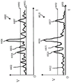
In the first embodiment, the twisted wire is formed into a loop of 8-shape, and the loop of 8-shape forms a quadrupole (gradient) having a long wire between two loops as shown in fig. 8Meter 1). The second embodiment is designed as a gradiometer 2 as shown in fig. 8. The figure-8 loop is about 5cm long, with each lobe having a diameter of about 2.5 cm. Fig. 9A-9C show sampled voltage waveforms collected from two sensors placed on top of a wireless energy source resonator configured to deliver 3.3kW to a load attached to the device resonator. FIG. 9A shows the small remnant voltage (-30 mV) on the two gradiometers shown in FIG. 8rms). The remnant voltage may be due to a combination of a non-uniform magnetic field, a slight change in lobe area, and electrical interference. The results from gradiometers #1 and #2 are plotted as curve 904 and curve 902, respectively. With the metal chewing gum foil placed on the right lobe of gradiometer #2, at least some flux through that lobe is blocked and the gradiometer becomes more unbalanced. In this case, a significant amplitude increase and a slight phase shift can be observed, as shown by curve 902 of fig. 9B. In the case where the foil moves to the left lobe of gradiometer #2, as shown in fig. 9C, the gradiometer is again unbalanced, causing a similar change in amplitude as in the case where the right lobe is blocked, but the phase changes by about 180 °. In some embodiments, these changes in the phase and/or amplitude readings of the FOD sensor or gradiometer can be used to detect the presence of FOD on the sensor. In certain embodiments, these changes in the phase and/or amplitude readings of the FOD sensor or gradiometer can be used to detect the position of the FOD on the sensor.
Embodiments of figure-8 sensors are also fabricated using Printed Circuit Board (PCB) technology to implement the sensor coil or loop. This embodiment may have advantages including: low cost, higher fill factor (since the loops can be made in any shape and are easily tiled using standard PCB processing techniques), higher uniformity, higher reproducibility, and smaller size, among other things. The use of a tiled rectangular loop for a 16-channel array of individual figure-8 sensors achieves a higher fill factor. The printed loop is highly uniform, whereby the baseline reading from the sensor is smaller (and flatter) in the absence of FOD.
In some embodiments, the above described sensors and/or gradiometer sensors may be combined with other types of FOD sensors to increase the detection probability and reduce false alarms (the system detects FOD in the absence of FOD). For example, a single temperature sensor or an array of temperature sensors may be integrated into the resonator assembly. If the FOD chip begins to heat up, the FOD chip may interfere with normal expected temperature measurements and/or spatial temperature distribution. The deviation may be detected and used to send an alert to the system controller. In embodiments, the temperature sensor may be used alone or in combination with a metal object sensor and/or may be used as a backup or confirmation sensor for the metal object sensor.
The presence of a living body, such as a person and/or animal, in the vicinity of the wireless power may be detected, and if a FOD is present between the source and the receiver, and/or if the living body breaks into a magnetic field having a particular field strength, the wireless power transfer system may be throttled down and/or shut down and/or an alarm or warning (e.g., a visual and/or audible signal) may be generated. The field strength limits that are allowable, acceptable, allowed, etc. may be frequency dependent and may be based on regulatory limits, safety limits, standard limits, public awareness limits, etc. In some embodiments, the dielectric sensor may measure a change in fringe capacitance from a conductor, such as a long wire, and may use the change to detect the proximity of a living being. In some embodiments, such sensors may be used during diagnostic testing, prior to wireless energy transfer, and during wireless energy transfer. In embodiments, such sensors may be used alone or in combination with any type of FOD detector. In certain embodiments, FOD detectors can detect humans, living organisms, biological substances, and the like.
Vehicle charging applications
Detection of FOD can be an important safety precaution in many types of wireless energy transfer systems. As an example, the detection of FOD by a 3.3kW vehicle charging system is discussed below.
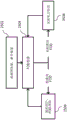
A block diagram of an exemplary EV charger system is shown in fig. 10. The system may be divided into a source module and a device module. The source module may be part of a charging station and the device module may be attached to an electric vehicle. Power may be wirelessly transferred from the source to the device via the resonator. Closed loop control of the transmitted power may be performed over in-band and/or out-of-band RF communication links between the source module and the device module.
The FOD detector system (not shown) may be integrated into various locations in the system. In some embodiments, the FOD system may be integrated into the source module, the source resonator, the housing or shell of the source resonator, or the like. In certain embodiments, the FOD system may be integrated on the device side of the system. In some embodiments, the FOD system may be implemented on both the source and the device of the wireless power transfer system. In certain embodiments, a FOD detection system may include a plurality of sensors and a processor having a discrimination algorithm. The processor may be connected to an interface that acts as an interlock in the source control electronics. Other FOD detector systems may be connected to the charger system through additional interfaces or through an external interface. Local I/O (input/output) at each module may provide an interface for system level management and control functions in a wireless power system utilizing FOD detection.
The source resonator in a high power (above 3.3 kW) vehicle charging system may have the highest magnetic field density near the boundary of the winding and optionally near any magnetic material. In the region of high magnetic field, a sensor array comprising a plurality of double figure-8 coils with rectangular lobes can protect the metal FOD from accidental heating. The array may be fabricated on a PCB and integrated filtering and signal conditioning may be included on the board. A second PCB of equivalent design may be slightly above or slightly below the first PCB and translated laterally in the manner described in fig. 4B. Alternatively, a multilayer PCB containing two (or more) sets of arrays on a single board may be used. The algorithm as described above may be run in an onboard processor, where the output of the onboard processor may be sent to a system controller. The system controller may compare the output of the metal FOD detector with the output of an additional FOD detector, such as a FOD detector that measures a temperature profile or dielectric change. Then, if FOD is detected, the system can decide whether to turn the system down or off.
Some possible operating modes of the FOD detection system are as follows:
Low power diagnostic tests can be performed without the presence of a vehicle to check the health and status of the charging station and to check the FOD before the vehicle drives past the source.
After the vehicle arrives and is above the source module, but before high power charging, the FOD detector can verify that there is still no FOD in the source and/or the area around the source.
After the vehicle arrives above the source module, but before high power charging, the FOD detector can verify that there is no FOD in the device.
During high power charging, one or more FOD detectors may verify that no additional FOD is moving onto or near the resonator coil.
If an FOD is detected during the low power diagnostics, a communication signal may be sent to the vehicle, charging station, central processor, etc. to indicate that an FOD is present at a certain source location. In some embodiments, the FOD sensor may include a communication facility. The communication may be in-band and/or out-of-band and may be part of an electric vehicle communication system, or may be a separate network. In some embodiments, a source may provide an indication to a user or driver that there is a FOD on or near the source. In some embodiments, the source may provide a visual indication, an audible indication, a physical indication, a wireless indication, and the like, to alert the user to the presence of the FOD. In certain embodiments, the resonator may include a mechanism for removing the FOD from and/or near itself, and such a mechanism may be activated in the event that the FOD is detected. In some embodiments, a user may have a device designed to remove a FOD from a resonator, and such a device may be used to clean the FOD from a system resonator, such as a source resonator and/or a device resonator and/or a repeater resonator.
In certain embodiments, a device designed to remove a FOD may include a magnet that may be used to attract a particular FOD, such as a metallic piece, a conductor, and/or a magnetic material. In some embodiments, devices designed to remove FOD may include brushes, brooms, swarfers, rags, mops, and sweeping materials, among others, that may be used to remove FOD. In certain embodiments, devices designed to remove FOD may include a vacuum, suction cup, tweezers, clamp, adhesive roller, blower, fan, and the like, which may be used to remove FOD.
Sensor data processing
In embodiments, readings from multiple FOD sensors in an array may be processed individually and compared to baseline or expected and/or measured readings from other sensors, sensor arrays, reference readings, stored readings and lookup values, and the like. In other embodiments, readings from multiple sensors may be used together and analyzed to analyze and compare the behavior of the entire sensor array. Processing and analyzing readings from multiple sensors simultaneously can provide improved sensitivity and FOD discrimination, among other things. In the present invention, it is understood that the processing and analysis may be performed at similar times. Processing multiple sensor readings together may provide more information due to the higher dimensionality of the data. Capturing and processing data from multiple sensors can capture effects such as interrelationships of adjacent sensors, trends and differences in the overall sensor system, and other effects that would not be captured if each sensor were analyzed individually. Some challenges to processing data from multiple sensors together may include ensuring that the data is processed efficiently and that possible information from the data is not lost during processing. With continuous detection of data, it can be difficult to store and analyze multi-dimensional datasets while maintaining the ability to detect small changes in the FOD sensor.
In some embodiments, readings from multiple sensors may be processed and analyzed together to calculate one or more numerical values that may be used as discriminators or alarms for abnormal system status or the presence of FOD. The data processing method may calculate one or more correlation, covariance, and mean matrices from the plurality of sensors that may be used as baseline values for comparing readings of the system. After the baseline is established, the readings from the sensors can be compared to the baseline using efficient matrix calculation to generate a probability or likelihood that the new reading is comparable to the baseline reading. The details of these exemplary steps are summarized below.
(i) Calculating sensor baseline
In some embodiments, to determine a baseline where FOD is not present, readings from at least two sensors in the sensor array may be used to calculate a mean and covariance matrix. The mean and covariance matrices can be used as a comparison of measurement data during operation for the FOD detection system.
In an exemplary embodiment, a FOD system has j sensors from each of which the amplitude r of the substantially sinusoidal signal from each sensor i can be capturediAnd phase thetai. Phase thetaiMay be defined by a reference value or signal. The user may determine the reference value or signal. In some embodiments, the reference signal may be generated from a reference clock circuit. In some embodiments, where the signal generated by the FOD sensor is not substantially sinusoidal, signal processing may be performed to substantially isolate and detect the fundamental component of the signal. In certain embodiments, where the signal generated by the FOD sensor is not substantially sinusoidal, signal processing may be performed to substantially isolate and detect at least one harmonic component of the signal. In some embodiments, any combination of fundamental and harmonic components of the sensor signal may be measured and utilized in the FOD detection scheme. For all sensors, the phase θ may be calculated with respect to one or more reference signals i. For j sensors, r for each sensori、θiProviding 2j data points. r isi、θiThe data may be represented as an array form x according to equation 1(Eq. (1)) as follows:
in some embodiments, there may be more than one reference signal for comparison. The plurality of reference signals may be generated via a plurality of reference coils in the FOD detection system. In some embodiments, the setting of the reference coil may be dependent on the magnetic field of the wireless power transfer system. For example, for a magnetic field that is radial in shape and perpendicular to the plane of the resonator coils of the wireless power transfer system, the reference coils may be arranged in a circle such that the field between the reference coils may be uniform. In another example, for a magnetic field parallel to the plane of the resonator coil of the wireless power transfer system, as shown in fig. 12, the reference coils may be arranged in columns or rows. The reference signal or set of reference signals from the reference coil may be compared to each other, to the signal from the FOD sensor, etc. A reference signal or set of reference signals may be utilized based on the location, size, type, and/or material of the detected FOD.
In certain embodiments, the readings of amplitude and phase from the at least one sensor may be processed and/or modified by a function, by circuitry, by calculation, etc., and the processed data may be represented in an array. In some embodiments, various functions may be used to process measurement data. In some embodiments, the functions used to process and/or modify the raw sensor data may not reduce the dimensionality of the data. For example, one function may take the sine and cosine of the phase of each reading, which results in the following array x according to equation (2) shown below:
In some embodiments, optionally, the value may be passed
Etc. to normalize each column of x.
In an exemplary embodiment, to construct a baseline mean and covariance matrix in which no FOD is present, the system may acquire multiple sets of sensor readings (e.g., p sets) to generate multiple data matrices x for various operating points of the system (power transfer levels, relative positions of source and device modules, etc.). The multiple readings of the sensor may preferably represent useful, common, specified and expected, etc. operating ranges of the system and sensor readings. With p sets of data (optionally normalized p sets of data), the mean μ and covariance σ matrix can be calculated according to equations (3) and (4) shown below:
in this exemplary embodiment, the covariance matrix σ may be a 2j × 2j matrix. The mean and covariance matrices may be saved by the system as baselines for comparison with sensor readings during normal operation. The mean and covariance matrices may be used to calculate the FOD likelihood during operation.
(ii) FOD likelihood calculation
In an exemplary embodiment, during normal operation, the system can collect readings from the FOD sensor and compare these readings to a calibrated baseline of the mean and covariance matrices to determine if FOD is present. The comparison may be based on a function that yields one or more numbers or likelihoods that are easy to analyze or compare. In one embodiment, if x is an array of 2j data points from j FOD sensors, the likelihood y can be calculated as shown in equation (5) below:
y=(x-μ)Tσ-1(x-μ) (5)
The probability Ψ may be calculated as shown in equation (5.5) below:
in an embodiment, the inverse of the stored covariance matrix σ may be pre-computed. The likelihood y may be used as an indication of FOD. In an embodiment, a threshold value may be assigned to the value of y, where sensor readings above or below the threshold value are assumed to detect an abnormal condition in the system, such as the presence of FOD.
In this exemplary processing technique and method, the behavior of multiple sensor readings may be used together in an efficient manner to determine the likelihood of an abnormal state of the system, and the data storage requirements for storing baseline or calibration readings are relatively small.
In an example embodiment, a system comprising one wireless source resonator and one wireless device resonator includes a FOD detection system. The FOD detection system includes a 7 x 7 array of figure 8 sensors (49 sensors total) between the source resonator and the device resonator. The figure-8 sensor is in the magnetic field of the source resonator. In the case of an oscillating magnetic field generated by the source resonator, the magnetic field generates a small oscillating voltage in the 49 FOD sensors. The voltage in a FOD sensor may depend on the magnetic field distribution around the sensor and therefore may act as a magnetic field gradiometer during operation of the system.
During normal operation of the wireless energy transfer system, the signal from the FOD sensor or the reading of the FOD sensor may change or drift due to changes in the magnetic field distribution caused by temperature changes, offset changes, power levels and the presence of other resonators, etc. Even in the absence of a FOD, sensor readings may change or drift during normal operation of the wireless energy transfer system. The system may require a calibration step to determine a baseline range of sensor readings or a range of normal sensor readings. The baseline readings may be used to compare FOD sensor readings during system operation (system standby, start-up, power transfer and maintenance, etc.) to detect FOD or abnormal system conditions that may appear in FOD sensor readings other than the baseline.
For an example system, a baseline may be established during a calibration process. The baseline may include a mean and covariance matrix calculated based on one or more of the system FOD sensor readings. To determine the baseline, the system may capture the amplitude and phase of the sensor readings for one or more system states (98 data points). The sensor readings for each state may be used to calculate the mean and covariance matrices as described above.
As beforeAs mentioned, it is assumed that p measurements are performed for calibration purposes. Each measurement of sensor data contains 98 values. Thus, each measurement x of sensor dataiCan be expressed as a column matrix of size 98 according to equation (6) shown below:
the p measurements of sensor data may preferably represent data generated for a range of operating points of the system in which FOD may be detected. With p measurements of the data (optionally normalized measurements), the mean μ and covariance σ matrices can be calculated according to equations (7) and (8) shown below:
after the system is calibrated and the mean and covariance matrices are saved and calculated, the system may periodically or continuously acquire measurements of the FOD sensor during operation of the system. For each set of readings from each sensor in the FOD system, the system can calculate a likelihood-based function y for FODs present in the vicinity of the system according to equation (9) as shown below:
y=(x-μ)Tσ-1(x-μ) (9)
the probability Ψ may be calculated as shown in equation (9.5) below:
the likelihood y and the probability Ψ may be used to determine the FOD likelihood. The maximum likelihood y corresponds to the minimum value of Ψ.
Based on an input, calculated, measured, or predetermined threshold for y, the system may classify the calculated value as being above the threshold (which means FOD is present) and use other parts of the system to mitigate or study the risk of FOD.
In some embodiments of the FOD detection system, the readings from each sensor may be given equal importance or equal weight in the calculation of the covariance matrix and the likelihood function. In some embodiments, the sensors may be given unequal weights or importance. In some embodiments, the readings from a particular sensor or sensors may be more important due to greater sensitivity and location of the sensors, etc. For example, some sensors (i.e., coils, loops, figure-8 loops) may be in a region of high magnetic field, while other sensors may be in a region of low magnetic field. It should also be understood that the various sensors described in this invention may be in the region of high magnetic fields, while other sensors may be in the region of low magnetic fields. In some embodiments, the changes detected by the sensors in the high magnetic field may be more important than the changes detected by other sensors in the system. Such sensors may be given greater importance and the readings of these sensors may be given greater weight in the calculation of the mean and covariance matrices.
In some embodiments, FOD sensors in high-field or "hot" regions of a resonator may be designed to be smaller and/or more closely spaced than sensors in low-field or "cold" regions. Regions where there is a transition from "hot" regions to "cold" regions may also have smaller sensor loops to minimize the effect of non-uniformity of the magnetic field within the region of the sensor loop. In certain embodiments, certain regions of a FOD sensor can include coils, loops, gradiometers, figure-8 sensors, etc., having lobes of unequal size and/or shape. Such asymmetric sensors may be designed to provide higher sensitivity, lower noise, and/or less temperature sensitive performance. In some embodiments, the sensor array may comprise at least one sensor having a different size and/or shape and/or symmetry, and/or type, and/or relative position, and/or relative orientation, and/or conductor material than at least one other sensor in the array.
In some embodiments, the system may have multiple baseline and/or covariance matrices. For example, the system may have a baseline and/or covariance matrix for one or more particular states, locations, temperatures, humidity, power levels, and the like of the system. In some embodiments, where the covariance matrix determined or calculated for a finite or particular baseline does not represent the entire operating range of the system, the system may be configured to activate the FOD detection system only if the system is in a particular state, location, power level, and/or range of states, locations, power levels, etc., for which the baseline was determined or calculated.
For example, the FOD detection system may only be calibrated with a baseline for sensor readings at a particular power transfer level (e.g., 3 kW). It should be appreciated that the FOD detection system may be calibrated with a baseline for sensor readings at a particular power transfer level of 0.5kW (e.g., 1kW, 2kW, 3kW, 4kW, 5kW, 6kW, 8kW, 10kW, 15kW, 20kW, 50 kW). The FOD detection system may use information from other sensors or portions of the system to determine whether the system is operating in a state where a baseline has been obtained. For example, the FOD detection system may receive information from the source resonator amplifier control circuit to determine whether the power transfer level is 3kW or about 3 kW. After the FOD detection system confirms the status of the system from other subsystems or sensors, the FOD detection sensor may be measured and compared to the saved baseline reading to determine if FOD is present. In an exemplary embodiment, the FOD detection system may include power level, location, system status, temperature and humidity detection capabilities. In such embodiments, the FOD detection system may confirm certain operating states without receiving information or system indications from other subsystems and/or sensors of the wireless power transfer system. In some embodiments, a combination of information and/or indications for more than one circuit, sensor, subsystem, etc. may be used to determine the operational status of the wireless power transfer system and the suitability of the baseline and/or covariance matrix stored in the FOD detection system.
In certain embodiments, a baseline and/or calibration may be calculated for sensor readings representative of normal and/or acceptable operation of the system. In some embodiments, the sensor readings used to calculate the baseline may be for FOD-free or fault-free operation of the wireless energy transfer system. The sensor readings used in the calibration of the baseline may represent part or the entire range of acceptable operating conditions of the wireless energy transfer system and part or the entire range of acceptable readings from the FOD detection system.
In general, various different operating states of the wireless power transfer system may be represented in the baseline and/or calibration information. In some embodiments, for example, baseline information may be provided (e.g., retrieved or measured) for a plurality of different operating states corresponding to different energy transfer rates between a power source and a power receiver of the system. In some embodiments, the baseline information may be provided for a plurality of different operating states corresponding to different alignments between the power source and the power receiver of the system. In some embodiments, baseline information may be provided for a plurality of different operating states corresponding to different spacings between a power source and a power receiver of the system, where the spacings are measured along a direction orthogonal to a plane defined by a resonator of the power source.
In certain embodiments, the sensor readings used to calculate or calibrate the baseline may indicate unacceptable system behavior or status. In some embodiments, the sensor readings used to calculate or calibrate the baseline may be readings for the presence of FOD in the vicinity of the system. The sensor reading used to calculate the baseline may be a resonator offset that is outside the operating range of the system. These unusual or undesirable system states can be used to construct their own mean and covariance matrices. These readings can be compared to sensor readings during normal operation by calculating the likelihood y to determine the likelihood that the readings match the readings used for calibration. If the likelihood is high, the system may determine that a FOD is present and initiate a system response to the detection event.
In some embodiments, a wireless power transfer system having at least one FOD detector system may use sensor readings to calculate or determine a baseline for normal or acceptable system operation and sensor readings to calculate or determine another baseline for undesirable or unacceptable system operation or status. In some embodiments, the system may have more than one stored baseline comprising one or more stored mean and covariance matrices. In certain embodiments, the one or more mean and covariance matrices may represent sensor readings for normal, expected, and/or acceptable system states and/or behaviors, and the one or more mean and covariance matrices may represent sensor readings for abnormal, unacceptable, and/or out-of-range system states and/or behaviors. In some embodiments, during operation of the wireless energy transfer system, the FOD detection system may take readings from the FOD detection sensor and compare these readings to acceptable and unacceptable baselines. The system can use additional processing to help determine whether the FOD sensor reading has a higher likelihood y than an acceptable or unacceptable baseline.
In some embodiments, during calibration and calculation of the baseline, the system may be trained or calibrated for a range of states and operating environments such that each state or environment has equal importance or equal weight in the calculation of the covariance matrix and likelihood function. For example, the status and operating environment may include source device separation distance, power level, frequency used in wireless power transfer, humidity range, temperature range, elevation level, and the like. In some embodiments, certain system states or environmental conditions may be given greater importance or weight in the calculation of the baseline. In some embodiments, certain specific system states may be more important or more likely during normal operation of the system. For example, systems used in the southern united states may be calibrated for a higher temperature range than systems used in the northern united states.
In some embodiments, a higher weight may be given to more likely system states in the calculation of the baseline. For example, during calculation of the baseline, more data points (more p measurements) may be collected from those states that may be more useful in normal operation. In some embodiments, a preferred method for establishing a baseline may include collecting baseline samples such that the number of samples collected for each state is proportional to the probability that the state exists during operation. In some embodiments, the preferred method may assign a weight to each state that is proportional to the probability that the state exists during normal operation.
As an example, if at baseline (x)1,x2,...,xp) Including p measurements, the p measurements may each be individually weighted (w)1,w2,...,wp). The mean and covariance matrices composed using this method can then be calculated according to equations (10) and (11) shown below:
(iii) synchronization
In some embodiments, a FOD system may include at least one conductive coil, wherein the at least one conductive coil picks up a voltage and/or current induced by an oscillating magnetic field. In some embodiments, the oscillating voltage/current signal may be used to determine quantities such as the frequency of the magnetic field, the amplitude of the magnetic field, and the phase of the magnetic field. These signals may be referred to as reference signals since these signals may be used for clock recovery and phase locked loops utilized by FOD systems. In some embodiments, the phase reference may also be set using a reference signal such that phase information from individual sensors may be defined relative to a reference phase. In certain embodiments, the coil used to detect the field used for wireless power transfer may be referred to as a "reference coil".
In some embodiments, the reference coil can be any shape and/or size, and can be supported by a similar conductor as the FOD sensor or made of a different conductor. In an exemplary embodiment of a FOD system including sensors integrated in a printed circuit board, the reference coil may be formed using printed circuit board traces, wire traces, litz wire traces, conductive strips, and the like. The reference coil may overlap a portion of the FOD sensor or may fit within a lobe of the FOD sensor.
In certain embodiments, a FOD system may include more than one reference coil. In some embodiments, FOD system operation may include methods to determine which reference coils or combinations of reference coils may be used in different operating modes. In some embodiments, signal processing for the reference coil signals may be used to determine whether one reference signal is better than the other reference signals, or whether multiple reference signals are better for a particular application. Parameters such as signal-to-noise ratio, harmonic content, and sampling sensitivity may be measured, calculated, and compared to determine which reference coil signals may be used in the FOD system.
As previously described, the output of each FOD sensor may be approximated by a sine wave. The presence of FOD may affect the amplitude as well as the phase of the sensor signal compared to the case where FOD is not present. To check the phase change of the signal, the reference signal may be measured, and any change in the phase of the sensor signal may be detected using the phase difference between the sensor signal and the reference signal. The reference signal may be generated by measuring the voltage across a loop of wire placed in a magnetic field. In the absence of FOD, the phase difference between the sensor signal and the reference signal may remain unchanged.
Thus, the phase difference of the sensor signal relative to the reference signal can be used for FOD detection.
(iv) Quadrature sampling
Quadrature sampling may be used to calculate the amplitude and relative phase of the measured sinusoidal signal with respect to the reference signal. In the case of FOD detection, the amplitude and relative phase of the measurement signal with respect to the reference signal may be used as parameters for classifying the measurement signal as either FOD present or FOD absent. In the case where the sampled signal is not perfectly sinusoidal, the relative phase of the orthogonally sampled trigger signal with respect to the reference signal may affect the calculation of the amplitude and relative phase of the measurement signal with respect to the reference signal. This may result in large dispersion of the calculated values of the amplitude and relative phase of the signal in the absence of FOD and reduce the sensitivity of the sensor. One solution to this problem is to ensure that the relative phases of the orthogonally sampled trigger signal and the reference signal are substantially constant. For example, the relative phase may be maintained within 10% (e.g., within 5%, within 3%, within 1%) of the average of the relative phases. The relative phase may be maintained by generating a quadrature sampled trigger signal using the reference signal to ensure that the relative phase of the sampled signal and the reference signal is substantially unchanged and/or to actively measure and control the relative phase of the sampled trigger and the reference signal.
The reference signal is processed using analog filters and amplifiers similar to the sensor signal. However, the gain of the reference signal may be selected to be different from the gain of the sensor signal amplifier.
Calibration of FOD sensor
In some embodiments, the FOD system and sensor may have a calibration process. This process can be used to "teach" or "train" the system normal operating limits or to calculate appropriate baseline data (e.g., averages and correlation matrices). It should be understood that suitable baseline data may also refer to parameters such as, but not limited to, the likelihood of the wireless power transfer system y, misalignment, temperature, humidity, and the like. The calibration process may involve collecting sensor data (x) at p states of the system to determine the average values and correlation matrix as described above. The calibration process may provide a limit or range of sensor readings in the absence of FOD. In embodiments, sensor readings may change or fluctuate due to movement of the resonator due to different resonator offsets, temperature changes, distance changes, or resonator types, vehicle changes, etc. The system may need to identify which changes in sensor readings are within normal limits of operation, and which are due to foreign objects near the resonator. In some embodiments, the system may require a calibration or teaching phase to identify sensor reading ranges and characteristics and may be considered to be within normal operation of the system and within normal limits of operation. The calibration operation may provide a baseline or range of baseline sensor readings classified as "normal" or "no FOD" readings. Sensor readings other than normal readings may be used to trigger an alarm signal and/or FOD detection or mitigation procedure.
In certain embodiments, the system may be calibrated at times during manufacture, after a period of regular use, and each time it is used. The type of calibration, time of calibration, complexity, number of readings, etc. may depend on the use case of the system, the desired sensitivity or performance, the cost of the system, etc. In some embodiments, the FOD detection system may utilize more than one calibration method. The system may be calibrated using one calibration method and another calibration method during use or in different environmental and/or deployment scenarios.
In some embodiments, the FOD detection system may be calibrated to a normal range or "FOD free" range of sensor readings during manufacturing or prior to system deployment. In some embodiments, the system may be calibrated or "trained" for a range of offsets, heights, resonators, resonator types, power levels, orientations, vehicles, temperatures, ground and weather conditions, and so forth. The teaching or calibration phase may be designed to provide sensor readings without foreign objects for the normal or expected range of expected use case scenarios. Calibration may be performed in a controlled environment to provide gradually new situation, offset, position and environment variables, etc. while taking sensor readings. The sensor readings may be taken continuously as the location and environmental conditions change, or periodically where the location or environmental conditions change in a significant manner.
For example, during a calibration process, the FOD detection system may be calibrated for changes in sensor readings due to changes in the offset or misalignment of the resonator. During the calibration process, the resonators may be offset or misaligned from each other. In the case where the resonators are offset from each other, the sensor readings may be continuously monitored and processed, even possibly with the resonators being transferring power. In some embodiments, the FOD detection system may be calibrated to accommodate changing conditions or environments using adaptive techniques. In certain embodiments, during calibration, sensor readings may be taken at discrete offsets, such as every 5mm, 10mm, or more offsets. In some embodiments, sensor readings may be taken at each measurement location or at certain measurement locations at multiple power levels or at continuously varying power levels. In some embodiments, a number of system performance parameters may be set, varied, and scanned to make measurements p for determining and/or calculating mean and covariance matrices.
In some embodiments, the covariance matrix of the system may be equal to the correlation matrix if the expected values of the system parameters, measurements, readings, etc. are zero. In this description, the terms "covariance" matrix and "correlation" matrix may be used interchangeably.
In certain embodiments, the sensor readings may be monitored during the calibration process, but only processed or stored if there is a significant change in the readings from the sensors. During calibration for various offsets, for example, the offsets may change and sensor readings may be monitored. The sensor readings may be processed, stored, or added to the calibration data only if the readings deviate from a predetermined threshold relative to the saved calibration data that has been acquired. Processing the data only if a change in the data occurs by a predetermined threshold reduces the number of readings and storage points required for a sufficiently accurate calibration.
Returning to the example of calibrating for a range of offsets using adaptive techniques, operating parameters of the wireless power system may be changed until the sensor readings are different from calibration data for the sensor that has been stored. After the readings differ significantly from the stored data or by a predetermined threshold, the sensor readings may be processed and added to calibration data for possible "FOD free" sensor readings during normal operation. In this regard, sensor data may be processed at non-uniform intervals. For example, calibration data may be acquired at 5mm, 20mm, 22mm and 24mm resonator offsets in the lateral-to-lateral direction from the difference between the sensor readings and the stored calibration data at those resonator offsets. Another calibration process on another wireless power system may include measurements taken at 10mm and 25 mm. The calibration process may be highly customized and may be optimized for calibration speed or accuracy or uniformity or any number of system variables, parameters, specifications, etc. In some embodiments, the calibration procedure for the FOD sensor includes at least one measurement of the at least one FOD sensor with the wireless power system in at least one mode of operation. In certain embodiments, where the wireless power system is in at least two modes of operation, the FOD calibration includes more than one measurement using at least two FOD sensors.
In some embodiments, calibration data stored in the system may be saved with the state of the system for each calibration point. The stored calibration data may be used to determine the state of the system during normal operation. For example, for each resonator offset position, calibration data may be saved along with information about the resonator offset position. During normal operation of the system, the system may use calibration to determine the offset of the resonator or other parameter of the state of the system in the event that the sensor produces a reading similar to that of a particular calibration point. In some embodiments, the calibrated FOD system may be used as a position sensor in a wireless power transfer system. In an exemplary wireless power transfer system embodiment, there may be "n" states that it may be desirable to distinguish based on sensor data. For example, the "n" states may be relative resonator positions. One of these "n" states may be (0,0,10), where (0,0,10) represents the relative position where the centers of the resonator coils are aligned in the xy plane and the resonator coils are spaced 10cm apart (following the (x, y, z) convention, where z is the dimension perpendicular to the x-y plane). The other of these "n" states may be (-5,10,15), where (-5,10,15) indicates that the resonator coil is offset by-5 cm in the x-direction, 10cm in the y-direction, and 15cm in the z-dimension. Such relative resonator position may be within a normal operating range of the wireless power transfer system, and the system may use the position data to enhance or alter operation of the system, including but not limited to tuning an impedance matching network, determining an appropriate power level, determining an appropriate drive frequency, and/or any combination thereof. In other embodiments, the relative position of the resonator may be determined to be out of range for the system, and the system control may generate an alarm, limit power turn on, initiate a relocation algorithm, and so on.
In an exemplary embodiment, the calibration data may be associated with certain system operating positions, orientations, power levels and frequencies, and the like. In such embodiments, baseline calculations may be established and/or stored for each operating state i. Each state i can be characterized using p data points (measurements) and can be represented as (x)(i,1),x(i,2),...,x(i,p)) Where i ranges from 1 to n or 0 to n-1, or values such that the set contains a range of n state values. For each of these n states, each state i may have its own mean and covariance matrix that can be calculated according to equations (12) and (13) shown below:
given a new measurement x, the most likely state of the system is determined by calculating the following matrix product as previously described and according to equation (14) shown below:
yi=(x-μi)Tσi -1(x-μi) (14)
equation (A) which can be shown below14.5) to calculate the probability Ψi:
The state with the highest value of y is the most likely state of the system. The highest value of y corresponds to ΨiThe minimum Ψ value in the distribution of (c).
Information in the readings of the FOD detection system relating to the state of the system may be used by other parts of the wireless energy transfer system. Information about resonator offset and resonator separation, etc., may be used by the power supply and control circuitry of the wireless energy source amplifier to control the power output of the source and output parameters of the source such as impedance, frequency, etc., based on the state of the system. In some embodiments, information from other sensors may be used to improve or supplement system state predictions from the FOD detection system. Information from temperature sensors, inductive-type sensors, power and voltage readings on the resonator, etc. can be used to supplement or improve the system state prediction from the FOD detection system.
In some embodiments, other devices or systems may use system state information. For example, in a vehicle charging application, the vehicle may use this information for guidance purposes to align the resonator during parking operations.
In some embodiments, each system may require a calibration process depending on the cost, tolerances, sensitivity requirements, etc. of the components used in the system. In certain embodiments, each FOD detection system may undergo an individual calibration process using a wireless energy transfer resonator and the system to be paired therewith. In some embodiments, each FOD detection system may use at least one special or standard wireless energy transfer resonator and system to perform an individual calibration process. The FOD detection system can then be paired with different groups of wireless energy transfer resonators.
In some embodiments, a calibration procedure for the FOD subsystem may only need to be performed for each type of wireless energy transfer system or resonator type. The test system may be calibrated once and the calibration data from one system may be used in all of the same or similar wireless energy transfer systems without having to recalibrate the systems.
In some embodiments, the calibration process may only need to be performed for each different type of wireless energy transfer system or resonator type. After the readings from the system type FOD detection sensors have been characterized, these readings can be used as baseline characteristic data for other similar systems, simplifying the calibration process for other copies of the system. With baseline calibration data loaded from the base system calibration, each successive system replica may only need to be calibrated at a particular subset of locations or system states to complete the calibration data acquisition for each system. In the case of small differences in system characteristics due to component variations, manufacturing uncertainties, and the like, additional calibration procedures may be required for each additional system copy.
In some embodiments, information from one characterization or calibration may be used in other systems. For some systems, it may be possible to compute the average matrix by scanning only one location, which may be the most likely operating location or state. The covariance matrix can then be calculated using this average, although the average is not strictly an average of all data points.
Assume that m measurements are taken in the most likely operating state and that the effective average μ can be calculated according to equation (15)eff。
The effective covariance can then be calculated by measuring p data points for all possible operating states but using the effective mean according to equation (16):
using this method, in case a new system is used, the effective covariance remains about the same and the calibration only requires a new effective mean, which can be measured faster since it is calculated for only one state of the system.
A system calibrated prior to deployment may be able to detect FOD at different stages of use and initialization of the wireless energy transfer system. In embodiments where the calibration includes sensor readings in the absence of a device resonator, the system may detect FOD before the device resonator arrives. For example, in a vehicle charging application, the source resonator may check for FOD before the vehicle arrives. In some embodiments, the wireless energy source may turn on or increase the power source before the vehicle arrives. The source resonator may boost power to full power or a portion of full power to excite the FOD detection sensor and obtain a reading. These readings may be compared to calibration data for a system operating and/or boosting power without an FOD. If these readings deviate from the stored calibration data, the user may be alerted of a possible FOD using the FOD detection system before the vehicle is parked on the source and/or before the wireless power exchange is partially or fully turned on.
If it is desired to conduct an inspection for FOD without the presence of a vehicle, the wireless power system source may need to energize the source coil without the presence of a device coil nearby. In this case, the source may energize the source coil in the same manner as it would if the device were present during normal power transfer, or may operate in a different mode to energize the source coil. For example, the impedance presented by the source coil in the absence of the device coil may not allow for proper operation of the source amplifier. In this case, there may be one or more elements in the impedance matching network that may be switched into the circuit to modify the impedance presented by the source coil in a manner that the amplifier and FOD detection system may be operated. After the FOD inspection is complete, the one or more components may be cut out of the circuit to allow normal power transfer operation in the presence of a vehicle.
A system calibrated prior to deployment may be immediately able to detect FOD in the vicinity of the wireless energy transfer resonator at system start-up. For example, after parking the vehicle and wireless energy transfer is turned on, the FOD detection sensor may be powered on and able to provide a reading that can be compared to the saved calibration reading. If the detected reading deviates from the stored value, the FOD detection system may generate a signal, alarm, indication, etc. indicating the presence of FOD. In some embodiments, the wireless power transfer system may operate differently in the presence of FOD than in the absence of FOD.
In certain embodiments, the FOD detection system may be calibrated during system deployment. In some embodiments, the FOD detection system may collect calibration data each time the system starts or begins energy delivery and/or when the system is delivering power at any level. In some embodiments, the system may perform system calibration during the beginning of energy transfer. In certain embodiments, it may be ensured that the system is free of FOD at system start-up. The FOD free environment of the system during start-up may be ensured by the user, by another system, by a FOD clearing device, etc. During initial wireless energy transfer, the system may use the initial FOD sensor reading as a baseline reading to be stored during operation, compared to the normal expected read array, and/or calibrated to the normal expected read array. In certain embodiments, during the first few seconds of operation or minutes of operation, one or more readings of the FOD sensor may be taken and used to calculate a reference or baseline for the sensor (i.e., calculate the mean and covariance matrices). It should be understood that calculating a reference or baseline for a sensor may also refer to calculating parameters such as, but not limited to, the likelihood of y, misalignment, temperature, humidity, etc. of the wireless power transfer system. During this calibration phase, the system may dither, change, or scan parameters of the wireless energy transfer system to provide a range of possible sensor readings during operation. Parameters such as power, phase, and frequency may be modified. After the baseline is established, the system can operate normally and continuously or periodically monitor the FOD sensor and compare to baseline readings calculated and measured during a calibration phase at system start-up. Sufficient deviation from the baseline reading can be used to indicate that the system state has changed and that FOD may be present.
In some embodiments, in the use of FOD calibration during system startup, calibration may be performed each time the system is moved, changed, or started. In certain embodiments, changes in system operating parameters such as resonator offset, distance, power level, temperature, and environment may result in significantly different FOD sensor readings that may not be due to the presence of FOD. Thus, the system can continuously add calibration data to the baseline matrix of calibration data over the lifetime of the FOD system. In embodiments, the FOD system may self-calibrate at system start-up and/or startup and/or during wireless power transfer. In some embodiments, various algorithms may be used to capture calibration data in the field. For example, the FOD system may collect calibration data at times such as every system turn on or every other system turn on or every nth system turn on (where n is a positive integer such as 10). In some embodiments, the system may collect additional calibration data at certain operating temperatures, power levels, coupling values, and the like. In some embodiments, the acquisition of calibration data may be adaptive and may change over time. For example, if calibration data has been collected for a temperature range that is deemed sufficient, the FOD system may no longer collect additional calibration data based on temperature readings. Although temperature is used as an example, any system parameter may be used, including but not limited to: a type of resonator, a certain separate resonator, a resonator attached to a certain vehicle type, a resonator at a certain power level, a resonator in a certain environment, and/or any combination thereof.
For example, in a vehicle charging application, the system may perform FOD sensor calibration whenever the vehicle is parked on the source. During calibration, after parking the vehicle, the source may initiate energy delivery and modulate parameters of the energy delivery while measuring the FOD sensor and calculating and storing the baseline. During initial calibration, the FOD in the resonator area may be cleared or checked manually or automatically to ensure the calculated sensor readings during normal (non-FOD or low FOD or non-hazardous FOD, etc.) operation of the baseline capture system. In some embodiments, the system may be recalibrated during initial start-up of the system each time the vehicle is parked and charged. Each time the vehicle is parked, the vehicle location, type, height, etc. may be different such that the previously captured FOD sensor calibration data is no longer representative of normal or expected FOD sensor readings at the current state of the system. In some embodiments, the previous baseline may be changed by recalibration. In some embodiments, the previous baseline may be discarded, overwritten, moved and ignored, etc., and the recalibrated baseline may be used independently. In certain embodiments, some combination of recent, previous, and stored calibration data may be used in the FOD detection algorithm. In some embodiments, the FOD detection system may be calibrated over time by a user and/or the system may include a self-learning or machine learning method to determine or learn normal and non-FOD sensor readings.
In another exemplary embodiment, the FOD sensor may include a printed circuit board. The printed circuit board may include traces that form conductive coils, loops, lobes, sensors, gradiometers, and/or figure-8. The conductive traces may be on a single layer of the printed circuit board, or the conductive traces may traverse multiple layers of the printed circuit board. Traces of an exemplary circuit board having 7 rows and 7 columns of square 8-shaped FODs are shown in fig. 16. The circuit board also includes a FOD sensor readout circuit 1602 and a synchronization coil 1604 for synchronizing the FOD sensor phase and magnitude readings with the oscillating field used for energy transfer.
Conductive traces can also be used to connect the FOD sensor to other electronics of the FOD sensor. In certain embodiments, a FOD system can include at least one FOD sensor connected to at least one electronic multiplexer. Exemplary multiplexers may be referred to as IC multiplexers, 2 x 8 multiplexers, and the like. In an exemplary embodiment, a FOD system may include an analog device IC multiplexer. In an embodiment, the FOD system may include an ADG1607BRUZ multiplexer or a multiplexer with similar functionality. In some embodiments, a plurality of multiplexers may be used to process the FOD sensor signals. In some embodiments, an IC multiplexer with a high input impedance may be in a FOD system.
In some embodiments, the FOD system may include a communication facility that enables the exchange of information between the FOD system and the wireless power transfer system and/or a controller of the wireless power transfer system. In some embodiments, the communication facility may be a wired facility and/or a wireless facility. In some embodiments, the FOD system is capable of sending and/or receiving information, control signals, alarms, reports, TTL signals, microcontroller commands, and the like. In certain embodiments, a FOD system may include a transceiver. In some embodiments, a FOD system may include a microcontroller.
In certain embodiments, the FOD sensor and/or system may be an add-on to an existing wireless power system. For example, the FOD sensor and/or system may be separately packaged to be attached to or rest on a resonator of a wireless power system and communicate with the wireless power system through a wired and/or wireless communication link. In some embodiments, the FOD sensor and/or system may be integrated into at least one component of the wireless power system. For example, a housing for a wireless power assembly may include a FOD sensor and/or system. As another example, a plastic cover assembled and affixed to the resonator housing may include the FOD sensor and/or system.
In certain embodiments, the FOD sensor may preferably sense an oscillating magnetic field of the wireless power transfer system or an oscillating electric field of the wireless power transfer system. In some embodiments, FOD sensors can be designed to sense primarily or exclusively oscillating magnetic fields and partially or minimally oscillating electric fields. In certain embodiments, a FOD system may be designed to substantially overlap a resonator coil of a magnetic resonator. In some embodiments, the FOD sensor may be substantially separated from the capacitive element of the magnetic resonator. In some embodiments, the conductive loop of the FOD system may be designed to be relatively insensitive to the oscillating electric field of the wireless power transfer system. In certain embodiments, FOD sensors can include shielding to minimize exposure and detection of these FOD sensors with respect to oscillating electric fields. In embodiments, additional "non-return" conductive traces can be added above and/or below the conductive traces of the FOD sensor. Fig. 17 illustrates an exemplary arrangement of non-return conductors 1702 to reduce the sensitivity of the non-return conductors 1702 (thick black traces) to ambient electric fields, where these non-return conductors 1702 may be utilized on one layer of the conductive layer of a PCB sensor array.
In certain embodiments, certain design approaches can improve the performance of FOD systems. For example, conductors for connecting the FOD sensor to the sensing electronics may be arranged such that the ambient field may be shielded. In some embodiments, it may be preferable to have the conductive traces run substantially one above the other, which is sometimes referred to as a "stripline" arrangement. Such orientation of the conductors may enable smaller and/or narrower conductive pads to shield these signal-carrying conductors from ambient fields.
In some embodiments, sensors may be used to detect system damage, system failure, housing penetration, or any other type of damage. System damage may affect sensor readings by completely blocking or altering one or more readings from the sensor. The erroneous sensor readings may be used to determine the type and extent of system damage. In some embodiments, a sensor or group of sensors may be able to serve as a back-up sensor for a damaged sensor. In some embodiments, a signal or message may be sent to a user of the system to notify the system of the corruption.
The presence of human tissue (hands, arms, etc.) can be detected by the inductive loop FOD sensor described herein. In some embodiments, the inductive loop sensor may be tuned to detect organic and/or biological tissue.
In certain embodiments, at least one FOD sensor may reside on the device side of the wireless power transfer system. The at least one FOD sensor may operate alone or in combination with the FOD sensor of the source side to improve detection performance of the wireless power transfer system for an article between the resonators. Signals from the FOD sensor may be used to determine other properties of the system such as the relative positions of the source resonator and the device resonator and/or resonator coil.
As previously described, other types of sensors, such as capacitive sensors, may be integrated with the metal FOD detector to provide additional detection capability for other types of objects that may be present in the area between or around the resonators. These additional sensors may operate independently of the metal FOD sensor, or the sensor signals may be combined and processed together with signals from the metal FOD sensor.
Misalignment and field detection
The wireless power transfer system may include a magnetic field sensor. The magnetic field sensor may be used in high power systems that deliver 50W, 200W, 1kW or more of power. According to an exemplary and non-limiting embodiment, the magnetic field sensor may be mounted on or near a source, device, or repeater resonator and/or component of the wireless power transfer system. In vehicle applications, for example, the magnetic field sensor may be located on or near source resonators, where these source resonators may be located on the ground, garage floor, road surface, or the like. The magnetic field sensor may be integrated, attached or located on or near the source resonator housing, electronics and other components. In some installations, the magnetic field sensors may be embedded in the ground, floor, concrete, asphalt, etc. near the source in a parking area around the vehicle. In some embodiments, the magnetic field sensor may be completely covered by a ground material such as concrete or asphalt, but the sensor may also be placed, attached or bonded to the top of the ground depending on the location where it is parked (e.g., public, private, indoor, outdoor, etc.). The magnetic field sensor may be integral with, attached to, or located on or near a device of the wireless power transfer system. For example, the magnetic field sensors may be attached at various locations around the bottom of the vehicle, around the perimeter of the vehicle, and within the cabin of the vehicle. The magnetic field sensor may be wired to the electronics of the wireless power transfer system that provides the readings. In some embodiments, the sensor may be wireless and may harvest or use energy captured from the wireless power transfer system and/or other energy source and may transmit the magnetic field readings to one or more components of the wireless power transfer system using a wireless communication channel.
In a wireless power transfer system configured for wireless charging of battery electric and hybrid electric vehicles, or other applications where large amounts of power are to be transferred, magnetic fields in user accessible areas may be monitored. For example, the magnetic field in the user accessible area may need to be kept low enough to meet human exposure and EMI/EMC regulations, for example. For the same power transfer level, variability in the alignment of the source resonator and the device resonator may cause greater or lesser magnetic field levels in these user accessible regions. A magnetic field sensor may be used to detect a high field, a change in field, or a particular distribution of fields, and indicate a potential high field in a user accessible area. The indication from the sensor may be used by the wireless power transfer system, and the system may, for example, reduce the level of power transfer such that the field is reduced. Rather than limiting power transfer to the same level for all resonator alignments in a wireless power transfer system, it may be desirable to sense the magnetic field in one or more locations and use this information in a feedback loop to control the level of wirelessly transferred power to operate at the maximum power level that can be transferred within regulatory limits, and/or other safety, user comfort, or interference limits. One or more magnetic field sensors located near the boundaries of the user accessible area (such as at the edge of a vehicle, on the source resonator housing, on the device resonator housing and near any resonators, etc.) may be used to determine whether the magnetic field in the user accessible area has exceeded certain safety regulations. In some embodiments, the readings from the magnetic field sensor closest to the user accessible space may be used alone, or may be given higher priority in a group of multiple sensor readings, and may be processed and used in a power control feedback loop. The power of the system may be adjusted based on such feedback and/or in conjunction with data input from other detection systems to ensure that the high-power wireless power transfer system is operating within established regulatory requirements.
In some embodiments, the magnetic field sensor may provide a direct or normalized reading of the magnetic field strength. The sensor may be calibrated to provide a reading that is proportional or correlated to the actual field strength. In some embodiments, the sensors may provide relative readings. In some embodiments, relative readings of multiple sensors may be used to infer or determine a potentially high magnetic field. For example, in a vehicle charging application, where the source resonator and device resonator of the wireless power transfer system are under the vehicle, it may be desirable to monitor potentially high magnetic fields around the perimeter of the vehicle to which a person standing near the vehicle may be exposed. To detect potentially high magnetic fields that may reach a person standing near the magnetic field of the vehicle, sensors may be located around the perimeter of the vehicle. The sensor may provide a direct reading of the magnetic field strength. In some embodiments, the sensor may be configured to provide an indication of the relative strength of the field in the vicinity of the sensor. The relative indication may be used to determine or infer a potentially high magnetic field due to misalignment of the device resonator and the source resonator. Misalignment of the resonator may cause a different magnetic field distribution than when the resonator is aligned. In some embodiments, the greater the misalignment, the greater the variation in the distribution. Relative readings from the sensors may be used to detect changes and potentially high magnetic fields in the user accessible region.
For example, with the source resonator and the device resonator aligned, the magnetic field distribution may be substantially uniform with respect to the left and right sides of the vehicle. In the aligned condition, the maximum field strength between the left and right sides of the vehicle may differ by 10% or less (e.g., 5% or less). In the event that the source and device resonators are misaligned, for example due to inaccurate parking, the field distribution may change with respect to the left and right sides of the vehicle and may not be as uniform as in the case of source and device resonator alignment. In some embodiments, the maximum field strengths between the left and right sides of the vehicle with the source and device resonators misaligned may differ by 11% or more (e.g., 20% or more). In some systems, the difference in field strength may be proportional or related to misalignment between the source resonator and the device resonator and/or potentially high fields outside the vehicle boundary.
In some embodiments, the system may be configured to monitor relative readings of the magnetic field sensors in different regions around the wireless energy transfer resonator. These relative readings may be compared to expected readings. In certain embodiments, the wireless system may be configured to reduce the level of energy transfer in the event that the difference between the readings between the sensors and the expected readings exceeds 15% or more. In some embodiments, where the relative readings between the sensors differ by 11% or more, the wireless energy transfer system may be configured to reduce the level of energy transfer. In certain embodiments, the power transfer level between the source resonator and the device resonator may be inversely proportional or inversely related to the relative difference in field strength readings between the sensors. For example, where the magnetic field strength readings between the left and right sides of the vehicle differ by 20%, the wireless energy transfer system may be configured to operate at 80% of the normal power level. In the case where the magnetic field strength readings between the left and right sides of the vehicle differ by 40%, the wireless energy transfer system may be configured to operate at 50% of the normal power level. It should be understood that the percentage values described are exemplary.
In some embodiments, the magnetic field sensor may be located near an area where potential high field exposure to humans or animals may occur, such as near the perimeter of the vehicle, near the seat and front of the vehicle, and so forth. In some embodiments, the magnetic field sensor may be in an area where there may be a relatively large change in the magnetic field distribution if the source resonator and the device resonator are misaligned. In some embodiments, for example, the magnetic field sensor may be located near or in line with the dipole moment of the source resonator.
In certain embodiments, the magnetic field sensor may comprise a coil of wire, a loop, a hall effect sensor, a magneto-diode sensor, a magneto-transistor, a MEMS sensor, and the like, and any number of voltage, frequency, or optical sensing methods may be used.
In certain embodiments, the FOD system and FOD sensor may be used to measure the field and/or relative field distribution around one or more resonators. In some embodiments, a system with one or more FOD sensors can be used to measure the relative distribution of the field around the resonator. When the resonator is misaligned, the field distribution around the resonator may change. A FOD system having one or more FOD sensors can detect changes in field distribution by measuring differential readings from sensors located near different portions of the resonator. Large or unexpected differences may indicate misalignment of the resonator, which may result in a field distribution that may extend into the user accessible area.
A FOD system may have one or more modes of operation. In one mode, the FOD system can be used to detect FOD, in another mode, the FOD sensor can be used to directly measure the field and field distribution, etc., to determine vehicle alignment and/or field strength. In some embodiments, readings from the FOD system may be processed simultaneously to determine or detect FOD and/or to provide potential alerts and indications of misalignment and/or misalignment that may cause high fields in human accessible areas.
An example embodiment of a method of using a magnetic field sensor to detect misalignment and/or potentially high magnetic fields in a human accessible region is shown in FIG. 23. In block 2302, a field sensor may take a reading of the field strength at or near the magnetic field resonator. The field readings may be collected by a sensor module of the wireless power transfer system and processed. In some embodiments, readings may be generated from a FOD system using a FOD sensor. In block 2304, the sensor readings may be used to determine field differences between the sensors. The sensor readings may be compared to each other. In block 2306, the sensor readings may be analyzed relative to expected readings or baseline readings. The baseline reading may include a sensor reading or differential range with the resonators aligned. The baseline readings may also include expected sensor readings or expected sensor reading differentials for various misalignments of the system. In some embodiments, the system may include a maximum likelihood calculation to determine the most likely misalignment of the system. In block 2308, based on the determined misalignment and/or direct sensor readings, a power level of the system may be adjusted to prevent a potentially high field in a user accessible location near the resonator.
In some embodiments, readings from external or other field sensors may be used by the FOD system. Misalignment information can be used to improve FOD readings and/or improve calibration of the FOD system.
It should be appreciated that although a magnetic field sensor is described in the above examples, a similar method may be used with an electric field sensor to detect potentially high or anomalous electric fields at, near or around the resonator and/or the electronic components of the wireless energy transfer system.
In embodiments, the FOD detection system may use more than one baseline and/or calibration file or configuration for the sensor, such as mean and covariance matrices. A baseline or calibration configuration can be used to define normal or expected readings from the FOD sensor. The calibration, baseline, and configuration files may include information for readings and/or thresholds used to determine the presence of FOD. For example, the baseline file may be a data file that includes information of baseline values (also referred to as "baseline parameters") such as a likelihood, a mean matrix, a covariance matrix, and the like. In some embodiments, the calibration file may be a data file that includes information such as a likelihood, a mean matrix, a covariance matrix, and the like. In embodiments, a baseline or calibration file or configuration may be defined for more than one position, misalignment, resonator type, and/or temperature, etc. In an embodiment, defining a calibration or baseline for normal or expected FOD sensor readings under no FOD conditions for a range of offsets or misalignments in the system may desensitize FOD detection. A calibration or baseline that defines a normal or expected FOD sensor reading for a range of resonator offsets or misalignments may have a greater range of expected or acceptable readings for the FOD sensor than a calibration that defines a baseline of a normal FOD sensor reading for one or a pair of resonator calibrations. A narrower baseline or calibration may increase the sensitivity or detection capability of the sensor.
In some embodiments of a wireless energy transfer system with a FOD detection system, more than one baseline and/or calibration file, range, and/or setting may be used. In some embodiments, if the position, environment, and/or misalignment of the resonator, etc. during operation is known, it may be preferable to use or load a baseline and calibration that defines expected or normal sensor readings under FOD-free conditions for a particular position, environment, misalignment of the resonator, or expected or normal sensor readings under FOD-free conditions for a narrower subset of possible positions, environments, misalignment of the resonator, etc. In some embodiments, the determination of baseline or calibration may be performed prior to energy transfer for a fixed location of the resonator to define a narrower baseline or calibration.
For example, a position detection system in a vehicle application may be used to determine misalignment of the resonator. The misalignment information may be used to select a particular baseline or calibration. If the misalignment is determined to be, for example, 4cm, a baseline or configuration configured to or representative of a normal FOD sensor reading for a misalignment of 4cm or less may be used. If the position or misalignment of the resonator cannot be determined, a baseline defining a configuration of normal FOD sensor readings for all acceptable offsets (e.g., 15cm or greater) may be used as a default baseline.
In another example, one or more readings of the FOD sensor may be taken during the first few seconds of operation or the first few minutes of operation, and used to calculate a reference or baseline for the sensor (i.e., calculate the mean and covariance matrices). It should be understood that calculating a reference or baseline for a sensor may also refer to calculating parameters such as, but not limited to, the likelihood of y, misalignment, temperature, humidity, etc. of the wireless power transfer system. After the baseline is established, the system can operate normally and continuously or periodically monitor the FOD sensor and compare to baseline readings calculated and measured during a calibration phase at system start-up. Sufficient deviation from the baseline reading can be used to inform the system that the state has changed and that FOD may be present. In some embodiments, where the alignment of the resonators is known for different temperatures and/or environments, for different source configurations, and/or vehicles, etc., a separate calibration file may be used if the wireless system is in a stand-alone configuration with the source without a coupling device.
FOD detection using a FOD system may be active or may be performed with one or more resonators coupled and transferring power. In embodiments, FOD detection using a FOD system may be active or may be performed without coupling of the resonators. In an example or vehicle application, where the source resonator is on or near the ground, and the device resonator is under the vehicle, FOD detection may be performed before the vehicle is parked or driven onto the source. In some embodiments, the FOD system may be activated periodically or when an incoming vehicle is instructed to check for FOD before the vehicle approaches. In the event that FOD is detected, an indication may be provided to a user, vehicle, or other part of the system that FOD is present and may need to be cleared before charging can occur. The indication of FOD before the vehicle is parked on the source may make it easier to clear the FOD and/or to check the FOD on or near the source resonator.
According to an exemplary and non-limiting embodiment, a FOD detection system may be calibrated for independent detection of FOD. Independent FOD detection can be performed in cases where a single resonator or group of resonators and their respective FOD detection systems are in an open environment and are not coupled to another resonator. The resonator or group of resonators may be a source resonator or device resonator paired with a FOD detection system. For example, in a vehicle application, a source resonator with a FOD detection system may be installed in a garage, parking lot, or other location where a vehicle equipped with a device resonator may be parked. In independent FOD detection, a source resonator paired with a FOD detection system may need to detect FOD in the absence of a device resonator. In some embodiments, for example, in the case where the vehicle and its device resonator are not on the source resonator, independent FOD detection may be performed in a vehicle charging application. In some embodiments, the FOD detection system and/or the source resonator may need to detect the presence of the device resonator, and may choose to calibrate accordingly. To support these operating modes, the FOD detection system may be able to detect FOD within a specified area with an acceptable error rate in the absence of another wireless power resonator or without strong coupling of another wireless power resonator. In an exemplary embodiment, the acceptable error rate may be equal to or less than 1 false positive per 100,000 readings. In another exemplary embodiment, the acceptable error rate may be equal to or less than 1 false positive per 1,000,000 readings.
In some embodiments, the FOD detection system may use different calibration files depending on the sensor environment. The calibration file may be a data file including identifiers related to the wireless power transfer system such as, but not limited to, temperature, humidity, power, frequency, range over source, and the like. In some embodiments, the baseline file may include information regarding temperature, humidity, power, frequency, range over the source, etc. related to the wireless power transfer system. In some embodiments, independent calibration of a FOD sensor and/or system can include calibration data, files, tables, and the like stored using the source (or any resonator associated with the FOD detector) and/or accessed by the source via wired or wireless communication to a server, database, cloud location, and the like. In an exemplary embodiment, the calibration data may be stored within the FOD detection system.
In some embodiments, the FOD detection system may be capable of tuning its operating frequency, and FOD measurements of various frequencies may be compared against each other and/or against at least one calibration file to determine the presence of FOD. In other embodiments, the baseline calibration file may be used as a comparison of measurements taken during FOD detection in the user's environment.
In some embodiments, independent FOD detection can detect FOD on the source surface and in the area above the source. In some embodiments, the height above the resonator at which FOD can be detected can be designated as Zspec. In an application of the FOD sensor to both the source resonator and the device resonator, the FOD sensor may only need to be at about Zspec=ZgapFOD detection in the region of/2, where ZgapIs the maximum specified resonator spacing that works with the expected efficiency. In an exemplary embodiment, ZgapCan be less than 5cm (e.g., less than 10cm,Less than 20 cm).
In some embodiments, the calibration scheme may be a continuous calibration scheme. The exemplary calibration scheme may be used for slowly varying conditions such as temperature and humidity. In other embodiments, the independent calibration may be a periodic or intermittent calibration scheme.
In some embodiments, calibration can be performed as part of the manufacture and/or installation of the FOD detection system. In other embodiments, calibration may be performed after installation.
In some embodiments, the source FOD detection system can use very low power to achieve independent calibration. For example, the source may not exceed 100W for FOD calibration. In some embodiments, the source may not exceed 50W for FOD calibration. In certain embodiments, the source may not exceed 300W, or 500W, or 1kW for FOD calibration.
An embodiment of a FOD detection method for independent FOD detection is shown in fig. 24. In block 2402, the FOD detection system may receive an indication to perform FOD detection. The indication may be received from another part of the system, e.g. a timer or the like. In some embodiments, FOD detection may be triggered by an indication of an incoming vehicle. The incoming vehicle may be configured to transmit an identification to a source of the wireless power transfer system when in proximity to the source. In some systems, the source may detect an incoming vehicle via a wireless communication channel, GPS location, or other means. The indication that the vehicle is approaching for charging may trigger the FOD detection system to activate and check the FOD before the vehicle arrives. In block 2404, a source or other portion of the system may perform a detection routine to check for the presence of a device. If no device is detected, the FOD detection system may perform a separate FOD detection routine. Detection of the device may be performed by sensing loading on the source, communication channel, and/or other sensors.
In block 2406, the source may be energized to generate a magnetic field to enable the FOD sensor to detect the FOD. In embodiments where the FOD sensor is a wire loop or differential loop as described herein, a magnetic field may be necessary for the sensor to make measurements. In some embodiments, the source may be energized and output a portion of its normal power, which may be limited to only generating enough magnetic field to activate the FOD sensor. In some embodiments, the source may be powered on and output at less than 5% (e.g., less than 10%, less than 20%) of its peak power. In some embodiments, the source may be energized and output 10W or more (e.g., 50W or more) of power. In some embodiments, the source may be powered by the same power source and amplifier used during normal wireless power transfer from the source. In some embodiments, additional amplifiers and/or power sources may be used to energize the sources. Smaller amplifiers may be used that may be more efficient at lower power levels. In some embodiments of the system, during independent FOD detection, the magnetic field required to activate the FOD sensor may be generated by a separate wire loop, coil, and/or resonator, etc., driven by a separate amplifier. The magnetic field used for FOD detection may not be generated by a resonator normally used for wireless energy transfer. Additional coils or loops configured to generate a magnetic field when energized by an oscillating voltage and/or current may be located at or near the FOD sensor coil. The coils that generate the magnetic field can be printed, assembled, or integrated with the FOD sensor coil.
In block 2408, the FOD detection system may load a particular configuration and baseline file for the individual FOD detection. The profile may be a data file that includes information of expected sensor readings, probabilities, mean matrices, covariance matrices, and the like. In block 2410, the FOD detection system can process the FOD sensor readings and apply the detection analysis described herein. If an FOD is detected, the FOD system may generate an indication of the FOD and send the indication to other components or portions of the wireless power transfer system, the vehicle system and/or a user, etc. For example, after detecting FOD, an indication of the FOD may be sent to the vehicle to alert the user of possible FODs on or near the source. The user may then know to check or clear the source of the FOD before parking and blocking the source.
FOD detection can be performed on a separately configured device resonator. The device can include an amplifier for energizing the device resonator to generate an oscillating magnetic field to activate the FOD sensor. The device may include additional loops and coils or the like integral with or near the FOD sensor to generate a magnetic field. Even if wireless energy transfer is not active, the loop or coil can be energized to generate a magnetic field to detect FOD in the vicinity of the device.
In the present invention, it should be understood that the information included in the "baseline file" may be included in the "calibration file" and/or the "configuration file". Similarly, information included in the "calibration file" may be included in the "baseline" and/or the "configuration file". Similarly, information included in the "configuration file" may be included in the "baseline" and/or the "calibration file".
Fixed location device identification
According to an exemplary and non-limiting embodiment, the source FOD detection system may be calibrated in the event that the device is moved to a fixed position relative to the source. For example, the source FOD detection system may be calibrated to include any potential effects of the presence of the device on the FOD detection program of the source FOD monitoring system when the vehicle with the device secured to the bottom side is first parked on the source and/or before a charging cycle is initiated between the source and the device. By including the device in calibration, the source FOD detection system can more accurately detect FOD that may be in the space between the source and the device. In an exemplary embodiment, the FOD detection system may be capable of detecting an introduced FOD before an independent FOD reading and after the vehicle has been parked. For example, the FOD detector may detect foreign objects that are dragged to the bottom side of the vehicle while the vehicle is parked and/or foreign objects that may fall from the bottom side of the vehicle onto and/or near the source resonator.
In some embodiments, a fixed location device identification calibration may be performed for each parking event. In other embodiments, the user may determine whether calibration is possible.
In some embodiments, there may be communication between the device initiating the fixed position device calibration and the source.
In some embodiments where the presence of the device resonator changes the field too much to enable the calibration process, the device resonator and/or resonator coil may be open, or short circuited, or driven with a current such that the change in the field of the device resonator and/or resonator coil is small enough to enable the source FOD detection system to function, calibrate, and enable, etc. In some embodiments, the device resonator and/or resonator coil may be driven with a signal that adjusts the magnetic field at the source so that fixed position device calibration may be initiated. In some embodiments, the device may be covered with a material that reduces the effect of the device on the source-side FOD detection system.
In embodiments where the FOD sensor may be directly driven by an applied electrical signal, the field of the source-side FOD detection system may be made as small as possible or may be generated at a frequency different from that of the device, such that the effect of the presence of the device on the source-side FOD detection system is minimized.
In some embodiments where the vehicle itself generates significant disturbances to the field of the source-side FOD detection system, there are parameters that identify the vehicle so that the source-side FOD detection system can account for the communication between the device and the source of the presence of the vehicle in a fixed position device calibration. That is, the FOD detection system may be capable of processing, adjusting, enhancing, etc., its calibration files and/or processes and its FOD detection algorithms to account for the presence of the vehicle.
Fixed position FOD detection
According to an exemplary and non-limiting embodiment, the FOD detection system can perform a fixed position FOD detection calibration in which the system can detect FOD with the device fixed in space relative to the source. For example, in a vehicle application, the FOD detection system may initiate a fixed position FOD detection calibration after a vehicle with the device attached to the bottom is parked over the source. In some embodiments, the system can perform a one-time FOD detection calibration. In some embodiments, data generated by a one-time FOD detection calibration may be stored and used until the device has been moved away from the source. This may occur, for example, if a vehicle with a device attached to the bottom drives off its parking spot. In some embodiments, the data generated by the one-time FOD detection calibration may be used as a calibration file as long as the charging cycle is running. If the charging cycle is interrupted or the restart is stopped for any reason, the fixed position device calibration can be re-run, followed by fixed position FOD detection. In some embodiments, the fixed position FOD calibration file may be compared to other calibration files and/or may be incorporated into existing calibration files and/or may be used to build custom calibration files and/or may be used to train the FOD detection system.
In some embodiments, fixed position FOD detection can detect Z above the source surfacespecFOD of/2 wherein ZspecIs the maximum specified resonator separation for operation between the source and the device in a wireless energy transfer system. Z above the FOD beyond the source surfacespecIn some embodiments of/2, the device-side FOD detection system may be responsible for detecting FOD.
Tolerance to misalignment
In certain embodiments, the FOD detection system may be calibrated to accommodate misalignment of a resonator relative to another resonator. For example, if a user of an electric vehicle equipped with wireless energy transfer capabilities repeatedly parks the vehicle within the range of positions of the source resonator, the FOD detection system may be calibrated to a range of parking positions that allows the user. The range may be specific to the user.
In some embodiments, a user may initiate or control such calibration. This may be useful where a user desires to train the FOD system at a rate different from that required. For example, a vehicle equipped with a wireless power transfer system and FOD detection system may change users and thus may need to be recalibrated for misalignment. The recalibration may be customized for each user.
Drift correction
In some embodiments, the FOD detection system may be calibrated to correct for drift in the detection of FOD. The sensitivity and/or specificity of a FOD detection system can change over time. This may cause the system to become more or less sensitive and deviate from normal operation over time. To compensate for this possible variation, the FOD detection system may be recalibrated to or towards its original factory set detection function, or reset itself to its original factory set detection function.
In some embodiments, in vivo test calibration can be performed during manufacture and/or installation of the FOD detection system. In other embodiments, such a test calibration may be performed after installation or when a user initiates calibration. In some embodiments, calibration, baseline determination, and detection may be performed in a similar manner as for a FOD sensor. During the calibration and baseline procedures, sensor readings may be taken under normal operating conditions in the absence of a living body. Based on the readings, a mean and covariance matrix may be calculated, where the mean and covariance matrix may be used to determine whether additional sensor readings fall within normal conditions or whether a living body is present.
Each of the above types of calibration may be employed alone or in combination with other types of calibration. The above types of calibration may each be employed by a FOD detection system associated with any resonator in a wireless power transfer system. That is, the FOD may be used by any and all resonators in a wireless power transfer system including a source resonator, a device resonator, and a repeater resonator.
In some embodiments where detection of FOD is obtained according to one or any combination of the above listed calibrations, the wireless energy system may be turned off, turned down, and/or locked based on the signal in the FOD detection system. In some embodiments, the operator or user of the vehicle is notified.
In some embodiments where the detection of FOD may be erroneous, the user may restart the calibration process. After the user resumes the charging process, one or any combination of the above listed calibrations may be initiated.
An example embodiment of a method for detecting FOD in a wireless power transfer system for a vehicle application using a FOD detection system is shown in the flowchart of fig. 25. In block 2502, the FOD detection system identifies a vehicle equipped with a device resonator when the vehicle reaches a parking area equipped with an active resonator. For example, the vehicle may be identified based on an identification signal transmitted by the vehicle and/or based on one or more detection loops mounted on the underside of the vehicle, wherein the loops generate an electrical signal when a portion of the field generated by the source resonator passes through the loops. The vehicle may measure these electrical signals and may send an identification signal to the source resonator. In some embodiments, the presence of the vehicle may be identified by an optical sensor and/or by a pressure sensor. The device resonator remains open.
In block 2504, the FOD detection system begins detecting any FOD in the wireless power transfer system. The detection includes detecting FOD that may be on or around the source resonator and FOD that has been brought about by the vehicle while parked. Such detection may be calibrated during manufacture or installation of the wireless power transfer system, also referred to as "factory calibration". In block 2506, the FOD detection system notifies the user whether FOD is detected. The FOD was cleared and the FOD detection was performed again. If an FOD is not detected in block 2504, wireless power transfer begins in block 2508. FOD detection continues and may occur continuously, intermittently, or periodically during wireless power transfer.
The wireless power transfer system stops power transfer if an FOD is detected during the wireless power transfer. The wireless power transfer is not resumed until the FOD is removed and/or the user of the system is notified. As shown in block 2504, after clearing the FOD, the FOD detection begins again.
In some embodiments, a liveness detection system may be capable of detecting a live object within a specified area with an acceptable error rate. In an exemplary embodiment, the acceptable error rate may be equal to or less than 1 false positive per 100,000 readings. In another exemplary embodiment, the acceptable error rate may be equal to or less than 1 false positive per 1,000,000 readings.
An embodiment of a foreign object detection system is shown in fig. 26. The system may include a plurality of modules, blocks, and components that may be used to detect foreign objects, and in some embodiments, living organisms (e.g., cats, mice, people, etc.) in the case of objects and organisms that are close to a resonator used for wireless energy transfer. In some configurations, the FOD system may receive location information from external sensors, vehicle information, or other sources. The location information may include or may be used to determine environmental parameters, resonator alignment, resonator distance, location of the wireless energy transfer component, relative location of the lossy object, and location of the region with the living organism. The system 2602 can use the change in position to change the calibration, adjust sensitivity, and detection algorithms, etc. of the system. For example, the field distribution around the resonators that transfer energy may change according to the shift in misalignment between the resonators. Changes in the magnetic field distribution can alter the readings of the FOD sensors in the system and can trigger false positives and/or reduce the sensitivity of the system to FOD detection. The system may load new configurations, change processing algorithms, and perform other functions to compensate for changes in sensor readings if location information is received.
In some embodiments, the system may also receive information regarding wireless power transfer parameters. These parameters may include data related to the status of the wireless power transfer, how much power was sent, at what frequency, at what phase, etc. In some embodiments, the system may also receive information from other sensors and system components. The system 2602 can receive information from temperature sensors, infrared sensors, pressure sensors, and the like, which can be used to change the calibration or baseline used by the FOD system, or to supplement the FOD readings.
A FOD system may include one or more FOD sensors and/or LOD sensors. The FOD sensor may include electrical conductors that form one or more loops as described herein. The LOD sensor may comprise an electrical conductor or other capacitive sensor. The FOD and/or LOD sensors may be formed using conductive lines formed on a printed circuit board or deposited/printed on a resonator package or other substrate. The sensor may be located and situated near the resonator, near high magnetic fields, near areas where living organisms may be present, and the like. In some embodiments, the sensor may be configured to be at a distance from the resonator, 10cm, or even 1 m. The sensors may be wired or wireless to receive power from a wireless power transfer system using wireless communication for data. The sensors may be coupled to readout circuitry that may sample and digitize sensor readings so that they may be processed by other modules of the system.
In some embodiments, a sensor such as a FOD sensor may require an oscillating magnetic field to activate the sensor. The oscillating magnetic field may be generated by a source resonator of the wireless power transfer system. The system 2602 may output instructions or directives to elements of the wireless power transfer system to generate a magnetic field using the resonator or to change a characteristic of the field generated by the resonator. In some embodiments, the system 2602 can include a field generator 2608 configured to generate an oscillating magnetic field to activate the FOD sensor. The field generator 2608 can include one or more loops coupled to the conductors of the amplifier. The amplifier can generate an oscillating voltage to drive the loops and generate a magnetic field.
In some embodiments, the system 2602 may be configured to have a calibration mode and a sensing mode, which may be selected based on external inputs or automatically selected based on sensor readings or the state of other elements of the system. During the calibration mode, the system may collect sensor information and generate configuration and baseline sensor data.
During operation in the calibration mode, a calibration engine 2612 of the system 2602 may be used to define a sensor configuration or baseline reading. In some embodiments, the calibration engine may be configured to detect an energy transfer condition. For example, the energy transfer conditions may include misalignment of the wireless power transfer system, temperature, humidity. The energy transfer conditions may include baseline parameters such as a mean matrix, a covariance matrix, and a likelihood. The calibration engine 2612 may include processes and routines for generating one or more sets of baseline readings. In certain embodiments, the baseline readings may include taking readings from one or more FOD and/or LOD sensors under normal operating conditions in which no FOD is present. Readings may be taken at different temperatures, orientations, offsets, and locations of the resonators, etc. These readings may be used to calculate a baseline, where the calculation may include calculating mean and covariance matrices as described herein. In some embodiments, the mean and covariance matrices may be calculated for different temperature, orientation, location, environmental conditions, and the like. The mean and covariance matrices, as well as other baseline readings and settings, may be stored in the calibration repository 2614. The sets of calibration and baseline readings stored in calibration store 2614 may be tagged or associated with particular temperatures, resonator locations, and environmental conditions, among others. The system may receive location, power level, orientation, temperature, etc. from external sensors and systems. The baseline and calibration files may be refined and updated periodically or in response to user input. For example, additional readings from the sensors may be collected periodically, and the mean and covariance matrices updated periodically.
In some embodiments, a calibration engine 2612 may be used to define a baseline reading in the presence of a FOD or living body. The calibration engine can capture sensor readings of temperature, orientation at various locations with FODs present near the system. In the presence of FOD or living organisms, the FOD and living objects can be used to train the system on expected or typical sensor readings.
During operation of the sensing mode of the system, the detection engine 2616 may be used to analyze readings from the sensors to determine if FOD or living bodies may be present on or near the resonator. Detection engine 2616 may receive readings from sensors 2604, 2606 and process the readings to determine whether the sensor readings indicate the presence of a FOD or living body near the sensors. The detection engine may compare the sensor readings to one or more baseline files or calibrations stored in the calibration repository 2614. The comparison may involve calculating the likely system states using the mean and covariance matrices as described herein. The detection engine 2616 may receive information about system position, temperature, alignment and energy delivery parameters, etc. to select the most appropriate baseline and calibration files. In some embodiments, the detection engine may use two or more different baseline and calibration files. Different baseline and calibration files may be used to improve sensor readings, confirm FOD detection, and reduce or increase sensor sensitivity, among other things. For example, in one embodiment, the system may first use a common baseline corresponding to a wide range of system positions and misalignments, and the like. Where a potential FOD reading is sensed, the system may use a different second baseline or calibration file to increase sensitivity or analytical discrimination. The second baseline may correspond to, for example, normal sensor readings for a narrow range of system positions and offsets.
In some embodiments, the sensing and calibration modes may run simultaneously. The calibration engine 2612 of the system may run concurrently with the detection engine 2616 of the system. If no FOD or living organism is detected, the calibration engine may use the readings to refine the baseline and calibration files.
During operation of the system 2602, one or more indicators 2618 may be used to display or notify the status of the system using visual or audio indications such as lights, graphical or visual displays, sounds, and the like. In the event that FOD is detected, for example, one or more lights may be activated to indicate to a user that a possible foreign object may be located near the resonator. In some embodiments, the system may also notify external systems and components of the system and FOD/LOD status. For example, an indication of the system status may be sent to the vehicle.
In the event that the detection engine 2616 detects an FOD or living organism, the system may initiate one or more countermeasures to move the FOD or living organism, as well as adjust the system to avoid foreign objects, etc. In one embodiment, the system 2602 may notify the wireless energy transfer system to change or adjust the wireless energy transfer. For example, the detection engine may be capable of classifying or determining the size and effect of the FOD or living subject, e.g., based on the size and/or phase of the electrical signal generated by the FOD and/or living subject sensor. The classification may include, for example, a simple binary classification scheme in which FODs and/or living organisms are classified as "problem" or "no problem". Different thresholds for the measured electrical signal can be used for FOD and live body classification. Based on the classification of the FOD, the system 2602 may indicate to the wireless energy transfer system to turn down power, change frequency, disable resonators, change resonator configuration, and so on. For some FODs, for example, energy transfer at full power (e.g., 3.3kW) may cause unacceptably high temperatures (e.g., 70 ℃) in the FOD. For example, reducing the wireless energy transfer power to half the power may limit the heating of the FOD to less than 70 ℃ (e.g., less than 60 ℃, less than 50 ℃, less than 40 ℃). In embodiments, a feedback loop with additional sensors, such as temperature sensors and infrared sensors, may be used to adjust the power of the energy transfer to reduce or control the heating of the FOD or to control field exposure to living organisms. In another example, in a wireless energy transfer system having two or more source resonators and/or device resonators, the resonators may be enabled or disabled conditioned on FOD sensor readings. Resonators that detect FOD nearby may be disabled or turned down to lower power, while resonators without FOD may operate at full power.
It is to be understood that the structure, order, and number of modules, blocks, etc. shown and described in the drawings of the present invention may be changed or varied without departing from the spirit of the present invention. For example, a module may be combined or divided into multiple other modules. For example, a single module may serve as both a calibration engine module and a detection engine module. The functions of the modules may be implemented using software, scripts, hardware, etc. For example, detection engine 2616 of system 2602 shown in fig. 26 may be implemented as a software module, as an application specific integrated circuit, as logic in a field programmable gate array, and so on.
Fig. 28 is a schematic diagram showing an example arrangement of a wireless power transfer system including one or more FOD sensor boards (also referred to as "FOD detection sensor boards") in a side view. One or more FOD sensor plates can be used to detect the magnetic field distribution generated by a source coil (e.g., a resonator coil of an electrical power source) or, optionally, an additional coil. Information related to the detected magnetic field (e.g., field distribution, field gradient distribution) may be used to determine misalignment between one or more resonators in the power source coil and one or more resonators in a power receiver within the apparatus. Coordinate 2840 shows an x-direction pointing in the right direction of the drawing plane and a z-direction pointing in the upward direction, respectively. The y direction points to the drawing plane.
At the top left of fig. 28, the arrangement 2800 includes a source coil 2802 of a power source resonator that can deliver power to a device coil 2804 (e.g., a power receiver resonator). The FOD sensor plate 2806 is between the source coil 2802 and the device coil 2804. In this example, the FOD sensor plate 2806 is placed a distance 2807 of about 10mm above the source coil 2802. In other examples, the distance 2807 may be between 3-5 mm (e.g., 4-8 mm, 5-10 mm, 7-12 mm, 10-15 mm, 15-20 mm). Distance 2807 may be greater than 20 mm. The FOD sensor board 2806 may be fixed relative to the source coil 2802 by a support structure (not shown) that holds the FOD sensor board 2806. For example, the support structure may be one or more posts that fix the FOD sensor plate 2806 relative to the source coil 2802. In some embodiments, a dielectric substrate may be placed on top of the source coil 2802, and the FOD sensor plate 2806 may be fixed on top of the dielectric substrate. In the example arrangement of 2800, the central axis 2803 of the source coil 2802 and the central axis 2805 of the device coil are aligned with each other. It should be appreciated that in the event that the device coil 2805 moves relative to the source coil 2802, the central axes 2803 and 2805 become misaligned. In this example, the position of the FOD sensor plate 2806 relative to the source coil 2802 is not changed by the support structure. Therefore, the FOD sensor board 2806 may be referred to as a "source-side FOD sensor board". In some embodiments, a FOD sensor plate 2806 may be used to determine misalignment between central axes 2803 and 2805 along the x-direction and the y-direction.
At the upper right of fig. 28, a setup 2810 includes a source coil 2812 of a power source resonator that can transfer power to a device coil 2814 of a power receiver resonator. The source coil 2812 has a central axis 2813 and the device coil 2814 has a central axis 2815. The FOD sensor board 2816 is between the source coil 2812 and the device coil 2814. In this example, the FOD sensor board 2816 is placed at a distance 2817 of about 50mm below the device coil 2814. In other examples, the distance 2817 can be between 5-15 mm (e.g., 15-25 mm, 25-35 mm, 35-45 mm, 45-55 mm). Distance 2817 may be greater than 50 mm. In this example, the FOD sensor board 2816 is fixed relative to the device coil 2814 and thus may be referred to as a "device-side FOD sensor board. The FOD sensor board 2816 can be used to determine misalignment between the central axes 2813 and 2815 along the x-direction and the y-direction.
At the bottom left of fig. 28, the arrangement 2820 includes a source coil 2822 of a power source resonator that may transfer power to a device coil 2824 of a power receiver resonator. The source coil 2822 has a central axis 2823 and the device coil 2824 has a central axis 2825. The FOD sensor board 2826 (as a source side sensor board) is fixed relative to the source coil 2826, and the FOD sensor board 2828 (as a device side sensor board) is fixed relative to the device coil 2824. The FOD sensor plates 2826 and 2828 can be used independently or in combination to determine misalignment between the center axes 2823 and 2825 along the x-direction and the y-direction.
At the bottom right of fig. 28, the arrangement 2830 includes a source coil 2832 of a power source resonator that may transfer power to a device coil 2834 of a power receiver resonator. The source coil 2832 has a central axis 2833 and the device coil 2834 has a central axis 2835. The FOD sensor board 2836 (as a source side sensor board) is fixed relative to the source coil 2836, and the FOD sensor board 2838 (as a device side sensor board) is fixed relative to the device coil 2834. In some embodiments, only one of the FOD sensor boards 2836 and 2838 may be present. The arrangement 2830 also includes an additional coil 2839 that is fixed relative to the source coil 2832. In other examples, the additional coil 2839 is fixed relative to the device coil 2834. The additional coils 2839 can generate magnetic fields and the FOD sensor plates 2836 and 2838 can be used independently or in conjunction with other detectors to determine misalignment between the central axes 2833 and 2835 along the x-direction and the y-direction.
It should be understood that the FOD sensor boards 2806, 2816, 2826, 2828, 2836, and 2838 may include FOD sensor arrays as described with respect to other figures (e.g., FIGS. 1-27) in the present disclosure. In some embodiments, the source coil and the device coil may operate between 10kHz and 100 MHz. For example, the source coil may transmit power at approximately 145 kHz. In other embodiments, the source resonator may transmit power at about 85kHz, about 44kHz, about 20kHz, about 250kHz, about 2.26MHz, about 6.78MHz, and/or about 13.56 MHz. In an embodiment, the source may have a tunable frequency. For example, the source may operate at a frequency of 145kHz + -10 kHz or 85kHz + -10 kHz. In embodiments, the operating range of frequencies may be ± 5%, ± 10%, or ± 20% of the center operating frequency. The source coil and device coil may be made of various conductive materials, including, for example, litz wire, solid core wire, copper tubing, copper tape, and any structure that has been coated with a highly conductive material such as copper, silver, gold, or graphene. In certain embodiments, the FOD sensor board may have a different shape and size than the source coil and the device coil. The FOD sensor plate may have a larger area size than the source coil or device coil to which it is fixed. For example, the width of the FOD sensor plate may be about 5 inches greater than the width of the source or device coil. In some embodiments, the size of the FOD sensor plate can be determined by the area of the magnetic field where the field is strongest. In other embodiments, the size and shape of the FOD plate may be determined by the area of certain objects that are judged to be heating to an undesirable level, or the size and shape may be set to be greater than such area by a factor such as 10%, 20%, 50%, or 100%, etc., to provide some additional "factor of safety" for the overall design. It should also be appreciated that the arrangements 2800, 2810, 2820, and 2830 may include shields that abut the source coil to reduce energy loss from the magnetic field generated by the source coil. Similarly, the arrangements 2800, 2810, 2820, and 2830 may include shields that abut the device coils to reduce energy loss from the magnetic fields generated by the device coils.
In some embodiments, FOD sensor boards 2806, 2816, 2826, 2828, 2836, and 2838 can be used to determine the distance between the source coil and the device coil in the z-direction.
Fig. 29 is a schematic diagram illustrating an example alignment between the source coil 2910 of the power source resonator and the device coil 2920 of the power receiver resonator, where the source coil 2910 and the device coil 2920 may correspond to the source coil and the device coil, respectively, shown in fig. 28. Coordinates 2940 show the x-direction and the y-direction. In fig. 29, the center of the source coil 2910 is fixed to x 0mm and y 0 mm. In this example, source coil 2910 has dimensions of 200mm × 200 mm. The settings 2900-2909 show the device coil 2920 at various positions relative to the source coil 2910.
The arrangement 2900 shows a device coil 2920 centered at 0mm x and 0mm y (also denoted 0 dx and 0 dy). The arrangement 2901 shows a device coil 2920 centered at 75mm x and 0mm y (also denoted as dx-75, dy-0). The arrangement 2902 shows a device coil 2920 centered at 0mm x and 75mm y (also denoted as 0 dx and 75 dy). The arrangement 2903 shows a device coil 2920 centered at 75mm x and 75mm y (also denoted as 75 dx and 75 dy). The arrangement 2904 shows a device coil 2920 centered at 150mm x and 0mm y (also denoted as dx-150 and dy-0). The arrangement 2905 shows a device coil 2920 centered at 0mm x and 150mm y (also denoted as 0 dx and 150 dy). The arrangement 2906 shows a device coil 2920 centered at 150mm x and 150mm y (also denoted as 150mm dx and 150mm dy). The arrangement 2907 shows a device coil 2920 centered at 300mm x and 0mm y (also denoted as 300 dx and 0 dy). The arrangement 2908 shows a device coil 2920 centered at 0mm x and 300mm y (also denoted as 0 dx and 300 dy). The arrangement 2909 shows a device coil 2920 centered at 300mm x and 300mm y (also denoted 300 dx and 300 dy).
FIGS. 30-39 and 41 show electromagnetic simulation results based on measurements using FOD sensor plates of settings 2900-2909. The FOD sensor board includes an 8 × 7 array of FOD sensors, and the graphs in FIGS. 30-39 and 41 show the measured voltage signals of each FOD sensor as gray square pixels. In these figures, the reference numerals dx and dy refer to the relative positions between the source coil 2910 and the device coil 2920, as described with respect to fig. 29.
Fig. 30 shows a graph of the simulation results for the FOD sensor board 2806 described in the setup 2800 of fig. 28. In this example, the source coil 2802 generates a magnetic field of current of maximum amplitude 3A that oscillates in the source coil 2802. In these simulations, the device coil 2804 was an open circuit such that there was substantially no current oscillation in the device coil 2804. The coordinate 3040 shows the x-direction and the y-direction. The FOD sensor plate 2806 detects a magnetic field at the position of the FOD sensor plate 2806 that depends on misalignment of the central axes 2803 and 2805 in the x and y directions. The figures 3000-3009 show the analog voltages measured by the FOD sensor board 2806 for the ten respective settings 2900-2909 shown in FIG. 29. The color bar 3050 represents a voltage amplitude between-0.5V and 0.5V.
The graph 3000 shows the voltage measured by each FOD sensor in an 8 x 7 array of FOD sensors in the FOD sensor board 2806. The measurement results of each sensor are represented by shaded pixels. For example, pixel 3021 represents a measured voltage signal of one FOD sensor in the FOD sensor board 2806, and pixel 3022 represents a measured voltage signal of another FOD sensor. Pixel 3021 corresponds to a higher voltage than pixel 3022. Thus, the FOD sensor board 2806 measures a voltage pattern. In 3000, the voltage pattern is relatively symmetrical about the axis 3031.
In some embodiments, for example, as described with respect to fig. 2, any FOD sensor may include one or more loops. In certain embodiments, any FOD sensor can include a figure-8 conductive loop.
3001-3009 show the voltages measured by each FOD sensor in an 8 x 7 array of FOD sensors in the FOD sensor board 2806 for different alignments of the source coil 2802 and device coil 2804 as represented by the arrangements 2901-2909. 3000-3009 have similar voltage patterns that are relatively symmetrical about axis 3031.
FIG. 31 shows 3100-3109 in a series of graphs generated by subtracting baseline patterns from the simulation results of 3000-3009 in the respective graphs. In this example, the baseline pattern is determined as the voltage pattern measured by an 8 x 7 array of FOD sensors in the FOD sensor board 2806 in the absence of the device coil 2804. The color bar 3150 represents the amplitude of the voltage between-0.02V and 0.02V. The voltage range is about 25 times smaller than the range of the color bar 3050 due to the subtraction of the baseline pattern, and 3100-3109 in the figure show substantially different voltage patterns relative to each other. Different patterns may be used as markers for determining the relative alignment between the source coil 2802 and the device coil 2806 where the relative alignment is unknown. For example, as a calibration step, voltage patterns for various known alignments between the source coil 2802 and the device coil 2806 may be experimentally measured. The experimentally measured patterns may be saved as a library in a data memory. Then, where the alignment between the source coil 2802 and the device coil 2806 is unknown, the voltage pattern can be measured using the FOD sensor board 2806 and the measured pattern compared to the patterns stored in the library to determine the degree of misalignment and/or the relative alignment between the source coil 2802 and the device coil 2806. The comparison results may be used, for example, to determine unknown alignments by determining matches between the measured patterns and patterns stored in the library. A match may indicate that the unknown alignment corresponds to an alignment corresponding to the matched saved pattern.
Referring back to FIG. 31, the voltage patterns 3107-3109 are difficult to visually distinguish from each other. In this case, the voltage pattern may be rescaled to adjust the color range of the respective map. FIG. 32 shows graphs 3107-3109 with rescaled color bars to clearly illustrate the respective voltage patterns of these graphs. 3107-3109 in the diagram in FIG. 32 visually show voltage patterns that are substantially different from each other due to the range of the rescaled voltages. These different patterns can be used to distinguish the corresponding alignments shown at 3107-3109 in the figure.
Fig. 33 shows a graph of the simulation result of the FOD sensor plate 2806 described in the setup 2800 of fig. 28. In this example, the source coil 2802 generates a magnetic field of current of maximum amplitude 3A that oscillates in the source coil 2802. In these simulations, the device coil 2804 was connected to a load, potentially through power conditioning, impedance matching, and resonant circuits, such that the current induced by the magnetic field of the source coil 2802 may oscillate within the device coil 2804. Coordinate 3340 shows the x-direction and the y-direction. The FOD sensor plate 2806 detects a magnetic field at the position of the FOD sensor plate 2806 that depends on misalignment of the central axes 2803 and 2805 in the x and y directions. 3300-3309 show the analog voltages measured by the FOD sensor board 2806 for the ten respective settings 2900-2909 depicted in FIG. 29. The color bar 3350 represents the voltage amplitude between-1.0V and 1.0V. In this example, 3300-3309 in the figure have voltage patterns that are similarly shaped but vary in voltage amplitude depending on the relative alignment between the source coil 2802 and the device coil 2804. For 3300 in the figure, the voltage amplitude is high (even higher than 3000 in the figure) due to the current in the device coil 2804. The change in voltage amplitude due to the change in relative alignment of the source coil 2802 and the device coil 2804 is greater than the curves 3000 to 3009 when the device coil 2804 is open. For example, the voltage amplitude in 3309 is about half smaller than the voltage amplitude in curve 3300. In some embodiments, a large variation in the measured voltage amplitude in the pattern may improve the accuracy of determining the relative alignment.
FIG. 34 shows a graph of simulation results by subtracting baseline patterns from the graph 3300-3309. In this example, the baseline pattern is determined as the voltage pattern measured by an 8 x 7 array of FOD sensors in the FOD sensor board 2806 in the absence of the device coil 2804. The color bar 3450 represents a voltage amplitude between-0.5V and 0.5V. As current is allowed to flow in the device coil 2804 during measurement, 3400-3403 and 3405 have a greater voltage amplitude than 3100-3103 and 3105 in the figure. The larger voltage amplitude improves the signal-to-noise ratio (SNR) of the measured voltage signal. In this example, 3400-3403 and 3405 in the figure show voltage patterns visually different from each other. In a similar manner to that described with respect to fig. 31, different patterns may be used as markers for determining the relative alignment between the source coil 2802 and the device coil 2806 where the relative alignment is unknown.
Referring to FIG. 34, the voltage patterns in the graphs 3404 and 3405 to 3409 are difficult to visually distinguish from each other. The voltage pattern can be rescaled to adjust the color range of the respective graph. FIG. 35 shows 3404 and 3405-3409 in a graph with rescaled color bars to clearly illustrate the variation of the respective voltage patterns between the graphs. As a result of the rescaling of the voltage ranges, 3404 and 3406-3409 in the graph in FIG. 35 visually show substantially different patterns that can be used to distinguish the respective alignments of 3404 and 3406-3409 in the graph.
In some embodiments, FOD sensors can have a large dynamic range that can measure voltage levels of 3400-3409 in the graph. FOD sensorIt is also possible to have high sensitivity and resolution for distinguishing the patterns 3404 and 3406-3409 in the figure. Thus, the FOD sensor can measure large voltage variations and can distinguish small variations. In certain embodiments, an analog-to-digital converter can receive a measurement signal from a FOD sensor. For example, a 20-bit analog-to-digital converter may provide 10 of the maximum detectable voltage of a FOD sensor-6Multiple resolution. In this example, if the maximum detectable voltage is 1V, the resolution may be 1 μ V. The analog to digital converter may be included in the control electronics described with respect to fig. 27.
FIG. 36 shows a graph of simulation results obtained for the FOD sensor board 2816 depicted in the setup 2810 of FIG. 28. In this example, the source coil 2812 generates a magnetic field of current with a maximum amplitude of 3A that oscillates in the source coil 2812. The device coil 2814 is open circuited such that there is substantially no current oscillation in the device coil 2814. Coordinate 3640 shows the x-direction and the y-direction. The FOD sensor board 2816 detects a magnetic field generated by the source coil 2812 that depends on misalignment of the central axes 2813 and 2815 in the x and y directions. 3600-3609 in the figure show the voltages measured by the FOD sensor board 2816 for the ten settings 2900-2909 depicted in FIG. 29. Color bar 3650 represents the voltage amplitude between-0.2V and 0.2V. In this example, 3600-3609 in the figure show different voltage patterns even without subtraction of the baseline pattern. By eliminating the step of subtracting the baseline, the method has the advantage of reduced computation time and cost.
In the example shown in FIG. 36, the voltage amplitude of the patterns shown at 3600-3609 in the figure strongly depends on the relative alignment between the source coil 2812 and the device coil 2814. This is because the FOD sensor board 2816 is a device side sensor board, and thus moves relative to the source coil 2814, producing a detected magnetic field. In the event that the FOD sensor plate 2816 becomes misaligned with the source coil 2812, the measured voltage changes faster than if the FOD sensor plate were fixed relative to the source coil. This approach may be advantageous since the measured voltage pattern may strongly depend on the alignment of the source coil and the device coil.
Fig. 37 shows a graph of simulation results obtained for the FOD sensor board 2816 depicted in the setup 2810 of fig. 28. In this example, the source coil 2812 generates a magnetic field of current with a maximum amplitude of 3A that oscillates in the source coil 2812. The device coil 2814 is connected to a load, and a current oscillates in the device coil 2814. Coordinate 3740 shows the x-direction and the y-direction. The FOD sensor board 2816 detects a magnetic field generated by the source coil 2812 that depends on misalignment of the central axes 2813 and 2815 in the x and y directions. 3700-3709 show the voltages measured by the FOD sensor plate 2816 for the ten settings 2900-2909 depicted in FIG. 29. Color bar 3750 represents voltage amplitude. Similar to the example of FIG. 36, the pattern of voltage amplitudes shown in the graphs 3700-3709 is strongly dependent on alignment position. However, the voltage patterns in the figures 3704, 3706, and 3709 are difficult to visually distinguish from each other. The voltage pattern may be rescaled to adjust the range of the respective graph. Referring to FIG. 38, the color bars 3704 and 3706-3709 in the figures are rescaled to show the respective voltage patterns of these figures. As a result, the patterns 3704 and 3406 to 3409 in the figure can be clearly distinguished. These patterns can be used to determine the respective alignments 3704 and 3706-3709 in the figure.
FIG. 39 shows a graph of simulation results by subtracting the baseline pattern from the graph 3700-3709. In this example, the baseline mode is determined as the voltage pattern measured by an 8 x 7 array of FOD sensors in the FOD sensor board 2816 in the absence of the source coil 2812. To measure the baseline pattern, the FOD sensor can measure the magnetic field generated by the current provided in the device coil 2814. For example, the current may be provided by a small power source connected to the device coil 2814.
3900-3909 show the voltage patterns after subtraction of the baseline patterns from 3700-3709. The color bar 3950 represents the voltage amplitude of the graph shown in fig. 39. After subtraction, 3904 and 3906-3909 in the figure show a much different voltage pattern compared to 3704 and 3706-3709 in the figure 37. Thus, subtracting 3900-3909 in the baseline pattern of the graph can improve the detectability of the alignment between the source coil 2812 and the device coil 2814 compared to the case of fig. 37.
Fig. 40 is a schematic diagram of a wireless power transfer system 4000 including a source coil 4002 of a power source resonator and a device coil 4012 of a power receiver resonator. The source coil 4002 is above the shield 4004 and the device coil 4012 is below the shield 4014. The source-side FOD sensor board 4006 is above the source coil 4002, and the device-side FOD sensor board 4016 is below the device coil 4012. The device coil 4012, shield 4014, and FOD sensor board 4016 are below the device cover 4018. In some embodiments, the area size of the FOD sensor boards 4006 and 4016 may be larger than the area size of the source coil 4002 and the device coil 4012, respectively. Coordinates 4040 show the x-direction and the z-direction. The system 4000 may include a magnetic material (e.g., ferrite) on either or both of the source side and the device side. For example, either or both of the source coil 4002 and the device coil 4012 may be wound with magnetic materials, respectively. It should be understood that the arrangement shown in fig. 40 is an example, and the relative separation and size may be modified.
The source coil 4002 and the device coil 4012 may each have a plurality of loops wound around an axis parallel to the x-direction such that an oscillating current in these loops induces a main magnetic dipole parallel to the x-direction. On the other hand, the FOD sensors in the FOD sensor boards 4006 and 4016 each have a plurality of loops wound around an axis parallel to the z direction, so that an oscillating current in these loops induces a main magnetic dipole parallel to the z direction. The wireless power transfer system may also include an additional coil 4020 that may be connected to a source of electrical power. The additional coil 4020 may be arranged such that the oscillating current within the coil 4020 induces a main magnetic dipole parallel to the z-direction.
In some embodiments, the FOD sensor may be more strongly coupled to the additional coil 4020 than to the source coil 4002 because the FOD sensor and the additional coil 4020 may induce a magnetic dipole in the z-direction. As such, the FOD sensor may be configured to detect the magnetic field generated by the additional coil 4020 and use the measured voltage to determine the alignment between the source coil 4002 and the device coil 4012. This approach may eliminate the need to power the source coil 4002 in order to determine alignment. Alternatively, the additional coil 4020 may be used with lower power than the power that would be required by the source coil 4002 to obtain a given voltage level detected by the FOD sensor. This can reduce the time required for position measurement, since the time required to activate the source coil 4002 is eliminated. In some embodiments, the additional coil 4020 is fixed relative to the source coil 4002. Optionally, the additional coil 4020 may be fixed relative to the device coil 4012.
Fig. 41 shows a graph of simulation results obtained for the FOD sensor board 4006 described in the system 4000 of fig. 40. In this example, the additional coil 4020 is a single wire loop having a current with a maximum amplitude of 1A that is different from the current with a maximum amplitude of 3A oscillating in the source coil of the example described in FIGS. 30-39. The device coil 4012 is open circuited such that there is substantially no current oscillation in the device coil 4012. Coordinates 4140 show the x-direction and the y-direction. The FOD sensor board 4006 detects the magnetic field generated by the additional coil 4020 that depends on the misalignment of the source coil 4002 and the device coil 4012 in the x direction and the y direction. The graphs 4100-4109 show the voltages measured by the FOD sensor board 4006 for the ten settings described in FIG. 29. The color bar 4150 represents the amplitude of the voltage. In this example, 4100-4109 show visually different voltage patterns without the subtraction of the baseline pattern. By eliminating the step of subtracting the baseline, the method may have the advantage of reduced computation time and circuitry. In some embodiments, the additional coil 4020 may have a plurality of wire loops that may increase the magnetic field generated by a current of maximum amplitude 1A oscillating within the additional coil 4020, thereby increasing the signal strength. In this case, if the signal strength is higher than the detectable strength of the sensor, the maximum amplitude current can be reduced relative to 1A, which can reduce the operating cost of the additional coil 4020.
In the examples described in connection with FIGS. 30-39 and 41, the measured voltage pattern may be compared to patterns in a library of a database. The comparison may be accomplished by statistically correlating the measured pattern with the stored patterns. Thus, the alignment of the source coil and the device coil providing the measured pattern may be determined to have an alignment corresponding to the saved pattern.
In some embodiments, a calibration step may be implemented to calculate and store a mean μ and covariance σ matrix, where the measured likelihood y and probability Ψ may be calculated using the mean μ and covariance σ matrices to determine the alignment between the source coil and the device coil. In this case, a smaller value of the probability y and a larger value of the probability Ψ represent a corresponding alignment of the measurements. For example, in a calibration step, j sensors in an FOD sensor array can measure data x in the form of an array according to equation (17) shown below:
wherein, | s1|…|sjCorresponding to the voltage amplitude of the respective sensor. In this step, x is measured for n states of different relative alignment positions between the source coil and the device coil. Each state i of the n states may be characterized using p measurements of various operating conditions (e.g., orientation, power level, frequency) of the system, and may be represented as (x) (i,1),x(i,2),...,x(i,p)) Where i ranges from 1 to n, 0 to n-1, or ranges of values such that the set contains n states. For each of the n states, each state i may have its own mean and covariance matrix that may be calculated according to equations (18) and (19) shown below:
given a new measurement x, the most likely state of the system is determined by calculating the following matrix product as previously described and according to equation (20) shown below:
yi=(x-μi)Tσi -1(x-μi) (20)
the probability Ψ may be calculated as shown in equation (21) belowi:
Minimum value of y corresponds to distribution ΨiMaximum of Ψ in (1). For a new measurement x, it can be determined that its respective relative alignment between the source coil and the device coil corresponds to the i-state having μ resulting in a maximum value of Ψ or a value of Ψ that is higher than a calibrated thresholdiAnd σi. It should be appreciated that this determination is different from the process of FOD detection, where the maximum value y of the likelihood in the process of FOD detection may indicate the presence of FOD. In some embodiments, based on the input, calculated, measured, or predetermined threshold of likelihood y, the power transfer system may classify the calculated value of likelihood y as being below the threshold of likelihood y to identify the alignment of the source coil and the device coil.
In FIGS. 30-39 and 41, patterns of voltage amplitudes are illustrated. In some embodiments, patterns may be generated from the magnitude and/or phase of the measured voltage and used as described above to determine alignment information between the power source resonator and the power receiver resonator. The method may provide additional information in determining the alignment between the source coil and the device coil. For example, in the calibration step, the data array x of j sensors can be measured according to equation (22) shown below:
wherein r isi、θiThe amplitude and phase of the measured voltage correspond to the j sensors, respectively. In another example, the data array x may be measured by taking the sine and cosine of the measured voltage according to equation (23) shown below:
it should be understood that at least some of the techniques described with respect to equations (1) - (16) may be applied to determine the relative alignment between the source coil and the device coil.
The graphs in FIGS. 30-39 and 41 show the analog voltages measured by the array of FOD sensors. In certain embodiments, an array of FOD sensors measures a pattern of induced current in the FOD sensors. In some embodiments, the FOD sensor can be a gradiometer that measures a voltage gradient. In this case, the techniques described with respect to FIGS. 30-39 can be applied to patterns of voltage gradients.
It should be understood that the FOD sensor board may have an array of sensors other than an 8 x 7 array. The number of sensors may be adjusted based on the resolution required to measure the voltage pattern. For example, a FOD sensor board may include any arrangement of sensors disclosed herein to measure a pattern of voltages and/or currents.
FIGS. 30-39 correspond to simulation results for a single FOD sensor board on the source side or device side. The techniques described with respect to FIGS. 30-39 can be applied to arrangements that use multiple FOD sensor boards (e.g., on both the source side and the device side).
The disclosed alignment measurement techniques may be used in vehicle battery charging applications. For example, the source coil may be connected to a source of electrical power at a home garage, driveway, parking lot, or other location where the vehicle resides for recharging, and the device coil may be secured to the vehicle. These techniques may be used to determine whether the device coil is sufficiently aligned with the source coil when the vehicle driver parks the vehicle over the device coil. For example, the centers of the source coil and the device coil may be aligned within 300mm (e.g., within 200mm, within 100mm, within 50 mm) of each other using these techniques. In some embodiments, where a device-side FOD sensor board is used, the measured position may be communicated to a visual or audio device in the vehicle through a hardwired or wireless connection. In certain embodiments, where a source-side FOD sensor board is used, the measured location may be wirelessly transmitted to a visual or audio device in the vehicle. The visual or audio device may then communicate information to the driver regarding the degree of misalignment between the vehicle and the power source, thereby prompting the driver to adjust the position of the vehicle as desired.
The disclosed techniques for determining relative alignment between two coils (also referred to as "alignment measurements") may be used in wireless power transfer systems that transfer power at any power level. Determining relative alignment through alignment measurements may help ensure efficient wireless power transfer and safe operation of the system. For example, a wireless power transfer system that transfers 2kW or more (e.g., 3kW or more, 5kW or more) (referred to as a "high power wireless transfer system" in the present invention) of power may be used to transfer power to industrial machinery or robots that may need alignment measurements with various power sources installed in a portion of a plant. In another example, a wireless power transfer system (referred to as a "low power wireless transfer system" in the present invention) that transfers power of 0.5kW or less (e.g., 0.1kW or less, 0.05kW or less) may be used as a wireless lighting system that may require a power transmitter on one side of a wall and a lighting device connected to a power receiver on the other side of the wall. In this case, the disclosed techniques can be used to align the power transmitter and power receiver to find the highest efficiency and optimal coupling alignment without easily seeing the sides of the wall for alignment of the resonator or coil. In some embodiments, the disclosed techniques for alignment measurement may be applied to a wireless power transfer system for powering lighting in a cabinet or electronic device, such as a display (e.g., TV, monitor, projector), or printer, etc.
In some embodiments, alignment measurements may be used in a wireless power transfer system that includes multiple wireless sources and receivers, e.g., in a room where one or more power sources may transfer power to one or more power receivers. In some embodiments, one or more power sources may be controlled to preferentially deliver power to one or more power receivers, and alignment measurements may be used to find an optimal best coupling or a most efficient alignment. In some embodiments, the repeater resonators may be aligned or positioned using alignment measurements to optimize the transfer of wireless power from one or more sources to one or more receivers. For example, the location of the repeater resonator in the room may be determined using the disclosed techniques for alignment measurements. This approach allows a user to easily position the repeater resonator relative to one or more sources or one or more receiver resonators in a room or space where it may be difficult for the user to visually align the resonators due to the presence of walls or objects blocking the user's view, which may be advantageous. For example, repeater resonators can be easily positioned around walls, corners, objects, under floors, in ceilings, and in furniture.
Fig. 42 is a schematic diagram of a source 4200 for wirelessly transferring power, where the source 4200 includes a sensor for detecting foreign matter. In this example, the sensors are LOD sensors, where each sensor measures a voltage signal induced by a capacitive change in the sensor due to the presence of an object (e.g., a living body).
In the top view of fig. 42, the source 4200 may include a PCB 4204 forming an active coil 4202. Source coil 4202 may be surrounded by a ground electrode 4206. Shield 4208 may surround ground electrode 4206. The sensor 4210 may surround the shield 4208. In some embodiments, for example, source coil 4202 has a width 4221 of about 20 inches and a length 4222 of about 22 inches. In the bottom cross-sectional view of fig. 42, the shield 4212 is on the other side of the PCB 4204 below the shield 4208 and the sensor 4210. In some embodiments, for example, the width 4223 of the ground electrode is about 1/2 inches, the width 4224 of the shield 4208 is about 1/4 inches, the width 4226 of the sensor 4210 is about 1/4 inches, the width 4227 of the shield 4212 is about 9/16 inches, and the distance 4225 between the ground electrode 4206 and the sensor 4210 is about 1 inch. More generally, however, each of these dimensions may vary widely depending on the particular application for which the source 4200 is delivering power to the power receiver. In some other embodiments, the source coil 4020 may be below the PCB (on the same side of the PCB as the shield 4212) rather than in the current position above the PCB shown in fig. 42. In this case, the sensor may be above the source coil 4020 (the current position of the source coil 4020 shown in fig. 42).
In certain embodiments, the shield 4208 may affect the distribution of the electric field formed around the source 4200 (e.g., by the source coil 4202 or the sensor 4210). For example, shield 4208 may be driven at the same potential as sensor 4210 such that the distribution of the electric field extends over a greater extent around PCB 4204 before reaching ground electrode 4206 than if driven at a different potential. The method may increase the detection range of the sensor 4210 by reducing the contribution of the electric field to the capacitive change of the sensor 4210. Thus, the shield 4208 may be used to block or reduce the effects of undesired electric fields on the sensor 4210. In this example, shield 4208 is not a ground electrode.
In some embodiments, the sensor 4210 may be a LOD sensor. For example, in the case where a living body approaches the LOD sensor, the LOD sensor may detect a capacitive change.
The source 4200 may be modified in a variety of ways. For example, fig. 43A is a schematic diagram of an LOD sensor arrangement 4300 including a source coil 4302 surrounded by a shield 4304. The setup 4300 may include a plurality of sensors. In this example, the shield 4304 is surrounded by sensors 4310, 4312, and 4314 disposed on the top and right side of the shield 4304. The shield 4304 is surrounded by sensors 4311, 4313, and 4315 disposed at the bottom and left side of the shield 4304. Dashed line 4320 indicates that sensors 4310, 4312, and 4314 are separated from sensors 4311, 4313, and 4315. Alternatively, sensors 4310, 4312 and 4314 may be connected to sensors 4311, 4313 and 4315, respectively. Dashed line 4320 also indicates that the shield 4304 is discontinuous at the location of dashed line 4320. This may prevent the formation of circulating currents having amplitudes greater than the damage threshold of the shield 4304. It is understood that dashed line 4320 may be located at the location of the setting 4300. In the example shown in FIG. 43A, the sensors 4310-4315 are each formed from a strip of a copper-based conductive material (e.g., metallic copper). The measurements from the plurality of sensors 4310-4315 may be used to determine the position of the moving object. For example, where a living body passes over multiple sensors 4310-4315, each sensor 4310-4315 may provide a peak in its measurement signal that differs in time from another sensor. By comparing the time differences, the speed and direction of the moving object may be determined.
In some embodiments, the sensors 4310-4315 may be discrete sensors. For example, the top of FIG. 43B is a schematic diagram of an array 4350 of LOD sensors including V-shaped sensors 4352-4354. In the case where the living body passes through the V-shaped sensors 4352 to 4354, the signals measured by the sensors 4352 to 4354 may be gradually varied instead of abruptly varied due to the shapes of the sensors 4352 to 4354. These measurement signals can be used to easily interpolate the position of the living body that can be located between two of the sensors 4352-4354. The bottom of FIG. 43B is a schematic of an array of LOD sensors 4364-4367 surrounding a shield 4362. The source coil 4360 is centered in the shield. Coordinates 4340 represent the x-direction and the y-direction.
In some embodiments, the signals measured with different sensors (e.g., signals corresponding to changes in sensor capacitance) may have different signal-to-noise ratios (SNRs). For example, referring back to FIG. 43A, the sensor 4314 may detect a signal level that exceeds the noise level of the sensor 4314, while the sensor 4310 may detect a signal level commensurate with the noise level of the sensor 4310 because the sensor 4310 is closer to the source coil 4302 that may be generating an electromagnetic field. The same type of noise may affect the measurements of sensors 4310 and 4314. In this case, the noise level of one sensor (e.g., sensor 4314) may be used to cancel or reduce the noise level of another sensor (e.g., sensor 4310), for example, by using weighted subtraction or correlation techniques. For example, the sensor 4310 may intentionally shield the presence of a detection object (e.g., a living body), so that the sensor 4310 may measure only noise. The sensor 4314 may measure signals from noise and the presence of a detection object. The effect of the signal from the presence of the detection object may be determined by subtracting the measured signal from the sensors 4310 and 4314 to eliminate or reduce the effect of noise. The method can be universally applied to a plurality of sensors.
Fig. 44 shows 4400 and 4410 in a graph, wherein 4400 and 4410 in the graph show examples of measurements from two sensors as a function of time (t) and voltage (V), respectively. The graph 4400 shows the voltage measurement result 4402 of one sensor, and the graph 4410 shows the voltage measurement result 4412 of the other sensor. The voltage represents the capacitive change detected by each sensor. The background level 4453 of the measurement 4412 is smaller than the background level 4451 of the measurement 4402. The SNR of measurement 4412 was about N times higher than the SNR of measurement 4402. The two measurements can be correlated with each other to eliminate noise affecting the two measurements 4402 and 4412. For example, in some embodiments, measurement signal 4402 can be subtracted from measurement 4412 after weighting their sizes based on the SNR ratio of measurement signal 4402 and measurement 4412. In doing so, the size of measurement 4402 may be reduced by a factor of N and then subtracted from measurement 4412. This approach may reduce the noise impact and improve the resulting SNR.
4400 has a threshold level 4450 and 4410 has a threshold level 4452. The threshold levels 4450 and 4452 may be determined by a calibration step. In some embodiments, the signals of the measurements 4402 and 4412 may be identified by voltage peaks that exceed respective voltage thresholds. For example, peaks 4404, 4405, 4406, and 4407 are identified as signals induced by a dielectric object in proximity to the sensor because their peaks are above threshold level 4450. Peaks 4414, 4415, 4416 and 4417 are identified as signals when a dielectric object is proximate to the sensor because their peaks are above a threshold level 4452. A comparison of the identified peaks can be used to determine useful peaks and to eliminate peaks caused by noise affecting both sensors.
In some embodiments, the comparison of the measurement signals of multiple LOD sensors may use the techniques described with respect to equations (1) - (23). For example, a calibration step may be performed to generate the mean μ and covariance σ matrices. At this step, the noise floor of the plurality of LOD sensors causing noise peaks or drifts may be included in the mean μ and covariance σ matrices. During the use of multiple LOD sensors to detect an object (e.g., a living body), the sensors may measure signals to provide a data array x, for example, in a similar manner according to equations (1), (2), (17), (22), and (23). In this case, the capacitance or change in capacitance measured by the plurality of LOD sensors is used to determine the array x. After the calibration step, for a new measurement x, the likelihood y and/or probability Ψ may be calculated using the techniques described with respect to equations (1) - (23) to determine the presence of a living body that induces changes in capacitance measured by the plurality of LOD sensors. It will be appreciated that the determination of the presence of a living body may be achieved in a similar manner to the techniques described with respect to the FOD detection process, but the data array x is obtained from a plurality of sensors based on capacitive sensing rather than from amplitude and phase data from magnetic field sensors. In certain embodiments, a large likelihood y may indicate the presence of a living body. Based on a threshold for the calculated, measured or predetermined likelihood y that is input, the power transfer system may identify that an LOD is present where the calculated value of likelihood y is the threshold for likelihood y.
Referring back to fig. 42, control electronics (e.g., a controller) may be connected to the sensor 4210 and the shield 4208. The control electronics may be tuned such that the combined control electronics and sensor 4210 system may have a minimum parasitic capacitance (C) that is the capacitance in the absence of a living body (e.g., a human or animal)p). This tuning step may increase the sensitivity of the sensor 4210 by enabling the controller to detect smaller changes in capacitance measured by the sensor 4210 due to the higher SNR. The capacitance change may occur by a dielectric object such as a living body approaching the sensor 4210. This approach may increase the maximum range of capacitance change detection of the sensor 4210. In some embodiments, the control electronics may be mounted in a location isolated from the metal components to reduce parasitic capacitance. The control electronics may be located at the corners of the source 4200. Parasitic capacitance can be reduced by shortening the routing connection length from the control electronics to the sensor. Instead of using extended wires to connect the control electronics and sensors, long sensors such as sensors 4310-4315, where the traces end up near the control electronics, can be used to shorten the connection length. Tong (Chinese character of 'tong') This approach may reduce parasitic capacitance by reducing the need for routing connections to the controller while increasing the area in which objects may be detected. In some embodiments, the controller may be turned off in the event that the power source connected to the source coil is turned on to avoid the controller detecting false peaks.
In certain embodiments, increasing the amplitude of the voltage applied to the sensor may increase the SNR of the sensor. The control electronics may operate at its highest voltage (e.g., 5V) to apply the highest possible voltage to the sensor. This approach may reduce noise inherent in the circuitry of the control electronics.
FIG. 45 is a schematic diagram of a source 4500 for wirelessly transmitting power, where source 4500 includes a sensor for detecting foreign matter. In this example, the sensors are LOD sensors, where each sensor measures a voltage signal induced by a capacitive change in the sensor due to the presence of an object (e.g., a living body). In the left side view of fig. 45, the source 4500 can include a PCB 4502 as a rectangular-shaped (e.g., square) strip surrounding an open space 4501. The sensor 4506 is above the PCB 4502 and extends as a strip along the left half of the PCB 4502. The sensor 4508 is above the PCB 4502 and extends as a strip along the right half of the PCB 4502. The shield 4504 runs along the outer perimeter as well as the inner perimeter of the PCB 4502. In the view on the right side of fig. 45, the cross-section of a portion 4530 of the source 4500 shows the shield 4504 partially wrapped around the PCB 4502 having a width 4220. For example, the width 4220 may be 1.5 inches. In some embodiments, another PCB 4503 may be a distance 4522 below the PCB 4502. For example, distance 4522 may be 1 inch. A ground electrode 4510 may be formed below the other PCB 4503. This approach can provide a lower parasitic capacitance of source 4500 to improve the signal-to-noise ratio of the signals measured by sensors 4506 and 4508.
Although the features described above in connection with fig. 40-45 relate to a source (e.g., a power source that wirelessly transmits power), some or all of these features may also be implemented in a power receiver that wirelessly receives power from a source. In particular, such a power receiver may comprise one or more resonators, which in turn may comprise one or more coils and one or more sensors configured to operate in the manner described above.
Multi-mode operation in vehicle charging applications
In vehicle charging applications, the detection system for LOD and/or FOD may operate in a number of different modes and switch between modes depending on the positional relationship between the vehicle and the wireless power transfer system. For example, the first mode may correspond to a situation where the vehicle is approaching the power transfer system but is not yet parked and power has not yet been transferred to the vehicle's on-board battery. The second mode may correspond to a situation where the vehicle has been parked near the power transfer system but transfer of useful power (i.e., power to charge the battery of the vehicle) has not yet occurred. The third mode may correspond to a situation where charging power is being actively delivered to a parked vehicle.
Fig. 46 is a schematic diagram of a flowchart 4600 showing steps for implementing operation in the first mode. In step 4602, a vehicle that is approaching the wireless power transfer system is detected, for example, using a communication signal that is wirelessly transmitted, such as via WiFi, bluetooth, or a cellular data network. In the event that a vehicle is detected, the mode 1 calibration file is loaded in step 4604, and the detection system checks to determine if a living body is present near the vehicle in step 4606.
If such an object is present, then in step 4608 the system issues a message (e.g., a visual message and/or an audible warning) that the living body is nearby and should be removed. If no such object is detected, the system checks for the presence of a foreign object near the vehicle in step 4610. If such foreign objects are detected, the system sends a message that foreign objects are present and should be removed in step 4612. If no foreign object is detected, the system waits for the vehicle to park on the wireless power transfer system in step 4614.
Fig. 47 is a schematic diagram of a flowchart 4700 showing steps for implementing operation in the second mode (i.e., after the vehicle is parked on the wireless power transfer system). In a first step 4702, the presence of a parked vehicle is checked, and then in step 4704, a mode 2 calibration file is loaded.
Next, in step 4706, the system checks whether there is a living body in the vicinity, and if such an object is detected, a warning is issued in step 4708 to remove the object. If no object is detected, the system checks whether there is a foreign object nearby in step 4710. If such foreign objects are detected, the system sends a message to remove the foreign objects in step 4712. If no foreign object is detected, the system waits for the start of power transfer between the wireless power transfer system and the vehicle in step 4714.
FIG. 48 is a schematic diagram of a flowchart 4800 showing steps for implementing operation in the third mode (i.e., actively transmitting power to a parked vehicle). As shown in a first step 4802, the process begins by starting to transfer power to the vehicle. Next, in step 4804, the system creates a mode 3 calibration file, and then in step 4806, stops power transfer to the vehicle.
The mode 2 calibration file is loaded in step 4808, and then the system repeats the mode 2 check for the presence of foreign objects near the power delivery system in step 4810. If such an object is detected, the system issues a message to remove the object in step 4820. If no such object is detected, the mode 3 calibration file is loaded in step 4812 and wireless power transfer to the vehicle is restarted in step 4814.
During wireless power transfer, the system checks for the presence of foreign objects using the mode 3 calibration file in step 4816. If no foreign object is detected, the mode 3 calibration file is updated as needed in step 4822 and the system continues to perform periodic checks for foreign objects in step 4816. If foreign objects are detected, power transfer is stopped in step 4818 and the system issues a message to remove the foreign objects in step 4820.
Generally, the steps shown in FIGS. 46-48 relating to checking for the presence of foreign matter and/or living organisms may be performed according to the methods described previously. The calibration files corresponding to modes 1, 2, and 3 of operation may correspond to the various types of calibration files previously described, which contain calibration data and other values corresponding to different modes of operation.
Multi-loop array for vehicle charging applications
Various different types of coils may be used in source resonators for vehicle charging applications. In particular, for certain vehicle charging applications, the source resonator may include a coil having a plurality of concentric loops extending in a common plane. Fig. 49 is a schematic diagram showing an example of such a coil 4902. As shown in fig. 49, the loops of coil 4902 are concentrically wound about a common axis and all expand in a common plane.
Fig. 50 is a schematic diagram showing the coil 5002 of the source resonator of the wireless power transfer system. Coil 5002, like coil 4902, includes multiple loops extending in a common plane (i.e., the x-y plane in fig. 50). Also shown in fig. 50 is a receiving resonator 5004 mounted to the bottom side of the vehicle (not shown) that receives power wirelessly transmitted in the z-direction from the coil 5002.
Where coils such as coils 4902 and 5002 are used for wireless power transfer, the spatial distribution of the magnetic field generated by the coils is an important consideration in FOD and LOD detection systems. In particular, to ensure that FOD and LOD are detected more accurately using detector arrays as previously disclosed, it may be desirable to ensure that the magnetic flux through the individual array detectors is as nearly equal as possible.
Fig. 51 is a schematic diagram showing the simulated magnitude of the magnetic field in the z-direction for a coil similar to coil 4902 or coil 5002. As shown, the field magnitude is greatest at the corners of the coil (i.e., where the density of the conductive elements of the coil is greatest) and approaches zero in regions outside the boundaries of the coil.
FIG. 52 is a schematic diagram showing simulated magnetic field magnitudes at a single corner of the coil shown in FIG. 51. As previously described, in some embodiments, an array of magnetic field sensors may be used to detect FOD by measuring perturbations in the magnetic field between a source resonator and a vehicle resonator in a wireless power transfer system. However, as can be seen from fig. 51 and 52, if a uniformly spaced array of similarly sized detectors is used, the flux through some detectors (e.g., those located closest to the corners of the source coil) will be significantly greater than the flux through other detectors.
In general, it may be desirable to minimize the dynamic range of the magnetic field flux through the detectors of the array. As mentioned above, one way to reduce this dynamic range is to use detectors of different cross-sectional areas. In particular, by using a detector with a larger cross-sectional area in the low flux region between the source resonator and the vehicle resonator and a detector with a smaller cross-sectional area in the high flux region, the dynamic range can be reduced relative to an array of equally sized detectors.
In some embodiments, varying the x-spacing and/or y-spacing between detectors may also be used to narrow the dynamic range of the magnetic flux through the detectors of the array. Further, in addition to using detectors different in x-pitch and y-pitch, detectors different in cross-sectional area may be used. In fig. 52, a dynamic range of about 5 can be achieved by using an array of 16 detectors that are sized according to vertical and horizontal lines that extend across the figure.
To further reduce the dynamic range, in some embodiments, detectors with different numbers of loops may be used. FIG. 53 is a schematic diagram illustrating an embodiment of a FOD/LOD detection system in which an array of detectors with different numbers of loops are used to narrow the dynamic range of flux through each detector. The quadrant of the source coil shown in fig. 53 is divided into 16 sectors, each sector corresponding to a different detector in the array. The reference numbers superimposed on the figure indicate the number of loops in each detector of the array.
Typically, detectors with a larger number of loops are used in the lower flux region, while detectors with a smaller number of loops are used in the higher flux region. Thus, for example, the detector 5302 in the region of low magnetic flux in fig. 53 has 3 loops. In contrast, detector 5306, which is in a high magnetic flux region, has a single loop. Detector 5304, which is in the middle flux region, has 2 loops. Note that in fig. 53, only the detectors 5302, 5304, and 5306 of the array are shown for clarity.
By varying the number of loops in one or more detectors of the array, a reduced dynamic range of magnetic flux can be achieved. For example, using the array shown in FIG. 53, the dynamic range of the magnetic flux can be reduced to values less than 2, allowing for more sensitive and accurate detection of FOD and LOD by the array.
In fig. 53, an array of 16 detectors is used to detect flux corresponding to one quadrant of the source coil. Thus, four such arrays (each featuring 16 detectors) are used to measure the flux from the entire coil. Typically, each of the four arrays is connected to an interface board, and then the four interface boards are connected to a common controller or control board.
In general, detectors having any number of loops may be used in the arrays disclosed herein. For example, a FOD detector having one or more loops (e.g., two or more loops, three or more loops, four or more loops, six or more loops, eight or more loops, ten or more loops) may be used. Furthermore, any combination of detectors with different numbers of loops may be used in a particular array for FOD detection. The detectors may be evenly or differently spaced and may have the same or different cross-sectional areas, depending on the particular geometry of the source resonator and measurement constraints.
Furthermore, an array having any number of detectors may be used for FOD detection. Although the foregoing example describes the use of four arrays each having 16 detectors, more generally, any number of arrays each having any number of detectors may be used. Furthermore, the number of detectors used in different arrays may be the same or different.
Additional FOD detection system and method
The previous section discusses a technique to detect FOD by measuring small perturbations in the magnetic flux extending from the source resonator to the vehicle resonator in a wireless power transfer system. Other methods can also be used for FOD detection.
In particular, in some embodiments (particularly where the source resonator is not actively transferring power to the vehicle), a method that does not rely on an active source resonator may be used to detect the presence of an FOD. Such an approach may be particularly useful, for example, in modes 1 and 2 of operation of the wireless power transfer system.
In certain embodiments, an auxiliary coil may be used to generate a magnetic field, and the perturbation of the auxiliary magnetic field is then detected by a detector array to determine the presence of FOD/LOD. Fig. 54 shows a vehicle resonator 5404 in the vicinity of a source resonator 5402. The auxiliary coil 5406 is in the vicinity of the source resonator 5402 and is connected to the same controller as the source resonator 5402 (not shown in fig. 54). The auxiliary coil 5406 generates a magnetic field, which is detected by the detector array 5408. Based on the signals measured by the detector array 5408, the system can use previously disclosed methods to determine whether FOD and/or LOD are present near the source resonator 5402.
An important advantage arising from the use of the auxiliary coil is that the frequency of the magnetic field generated by the auxiliary coil may be different from the frequency of the field generated by the source resonator 5402. By using a measurement frequency different from the frequency employed for transmitting electric power from the source resonator 5402 to the vehicle resonator 5404, the influence on the measurement signal that may be generated due to dynamic variations during electric power transmission is eliminated. Furthermore, if the power transfer frequency and the measurement frequency are sufficiently different from each other, the disturbance of the sensor signal due to the current induced in the source resonator or the vehicle resonator is eliminated. As an example, if power is transferred between the source resonator 5402 and the vehicle resonator 5404 at a frequency of 85kHz or 145kHz, the auxiliary source 5406 may generate a magnetic field at a significantly higher frequency (such as 6.78MHz, etc.) and/or a significantly lower frequency (such as 8kHz or less, etc.).
In some embodiments, to further ensure that the magnetic field generated by the auxiliary coil 5406 and the induced currents in the detector array 5408 do not disturb the source resonator 5402, the fields generated by the source 5402 and auxiliary coil 5406 may have different phases. For example, in some embodiments, the fields may differ in phase by 30 degrees or more (e.g., 60 degrees or more, 90 degrees or more, 120 degrees or more, 150 degrees or more, 180 degrees or more).
In certain embodiments, an auxiliary amplifier may be coupled into the source resonator and the source coil used to generate a magnetic field for detecting the FOD/LOD without using the source coil to transfer power to the vehicle resonator. The use of a source coil (e.g., the coil of the source resonator 5402 in fig. 54) to generate the measurement magnetic field may have a number of advantages. For example, the same detector array may be used for FOD/LOD sensing in modes 1, 2, and 3. Furthermore, since it may not be necessary to implement an auxiliary coil, system design may be simplified.
In the case of coupling the auxiliary amplifier into the existing source resonator, two significant consequences should be avoided. First, the auxiliary amplifier should be prevented from back-driving the power amplifier that normally drives the source coil to generate the magnetic field for wireless power transfer. Secondly, the auxiliary amplifier should be prevented from inducing a current in the vehicle resonator.
In general, power amplifiers using relay-off sources may introduce unacceptable power losses in wireless power transfer systems. Therefore, it is preferable to introduce the auxiliary amplifier in a way that does not require decoupling of the power amplifier. Thus, in some embodiments, the auxiliary amplifier is behind inductor L3 and capacitor C3 in the source impedance matching network, and a switchable slot is used across L3 to avoid a reverse-driven source power amplifier.
Fig. 55 shows a schematic circuit diagram of one embodiment of a wireless power transfer system with a switchable auxiliary amplifier 5502. Switch S during wireless power transfer to a vehicle resonator1And S2Is turned off so that the auxiliary amplifier 5502 is decoupled from the system. Power amplifier drive coil L of a systemsThis generates a magnetic field for wireless power transfer.
To measure FOD/LOD, auxiliary amplifier 5502 is operated by closing switch S1Coupled into the system. At the same time, switch S2Is also closed, thereby producing the use of the capacitor CTBlocking the slot circuit. The blocking tank circuit prevents the auxiliary amplifier 5502 from driving the power amplifier of the system. Instead, auxiliary amplifier 5502 drives coil LSThis isThe sample generates a measuring magnetic field for detecting FOD/LOD. To ensure that the measurement field does not induce a current in the vehicle resonator, the auxiliary amplifier 5502 drives the coil L at a frequency substantially different from the power transfer frequency, as described above S. In some embodiments, auxiliary amplifier 5502 drive coil L may be selectedSThe frequency used in order to minimize the current induced in the vehicle resonator.
In some embodiments, the impedance matching network of the source does not include the inductor L3. In such an embodiment, the switchable capacitor C introduced in fig. 55 may be usedTIn a similar manner by introducing a switchable inductor L across the capacitor C3TTo implement a blocking slot circuit.
In certain embodiments, FOD detection may be performed by measuring inductance changes in one or more detectors. As mentioned above, FOD detectors disclosed herein generally include one or more loops of conductive material. The presence of metallic FOD in the vicinity of the sensor can affect the inductance of the FOD sensor loop, since metallic FOD can affect the magnetic field generated by the current flowing in the sensor loop. Thus, a measurement of the inductance of the FOD detector can be used to detect the presence of FOD in the vicinity of the detector.
Fig. 56 is a schematic diagram showing an array of detectors 5602 connected to an inductance measurement controller 5604. Typically, the detector 5602 is between or around a source resonator and a vehicle resonator of a wireless power transfer system. To detect the presence of FOD near the source resonator, the controller 5604 measures the inductance of each detector 5602. FOD is detected based on changes or deviations in inductance measurements from expected/calibrated values of the array. Suitable controllers for measuring changes in inductance of detector 5602 include, for example, an LDC1000 controller available from Texas Instruments (dallas, Texas).
In an FOD detection system that measures changes in inductance of a detector coil, for example, as shown in fig. 56, each detector functions as a resonant LC circuit. Thus, where the detector is integrated onto a detector PCB (see discussion of fig. 57A and 57B below), the PCB includes an array of coupled resonators. In case a foreign object perturbs the inductance of a particular detector (i.e. resonator) in the array, nearby detectors (i.e. resonators) are also affected due to the mutual coupling of these detectors (i.e. resonators). Thus, a measurement change in inductance and/or resistance of a particular detector is affected not only by foreign objects near that detector, but also by foreign objects near adjacent detectors. This "amplification" or "distribution" effect due to resonant coupling between the detectors in the array can significantly improve the sensitivity of the entire array to foreign objects, thereby improving the accuracy with which the system can detect these objects.
In the current and preceding sections, various measurement methods are disclosed for detecting FOD/LOD in a wireless power transfer system. It should be understood that these methods may each be used in various modes of operation of such systems, and that different methods may be combined and/or used in different modes of operation of the same system.
For example, magnetic field sensing (i.e., detecting a perturbation of the magnetic field generated by the source resonator) may be used in all three modes of operation, and is particularly useful in the third mode of operation where power is actively transferred from the source to the vehicle resonator. FOD detection via the auxiliary coil can be used for all three modes of operation and is particularly useful for modes 1 and 2 where the source resonator does not actively generate a magnetic field. Similarly, inductance measurements for FOD detection can be used for all three modes of operation, and are particularly useful in modes 1 and 2 where the source resonator does not actively generate a magnetic field. As shown in fig. 55, a wireless power transfer source including a switchable auxiliary amplifier typically uses the auxiliary amplifier to generate a measurement magnetic field in modes 1 and 2 of system operation, and uses any other method described herein to detect FOD if the system is operating in mode 3.
Fig. 57A illustrates an exemplary embodiment of a FOD detection system. In some embodiments, the FOD detection sensor board can be made of multiple circuit boards 5706A-D. This is beneficial for mechanical assembly with the intercommunication board 5704 and the electronics board 5702. In addition, by dividing the FOD detection sensor plate into a plurality of plates, the cost can be reduced. For example, one large printed circuit board may be more expensive than four smaller printed circuit boards. The interconnection plate 5704 provides a connector 5707 so that signals from the FOD detection sensor plates 5706A-D have a path to the electronic board 5702. The electronics board 5702 may include power and control circuitry, communication and signal processing capabilities.
FIG. 57B shows a top view of an exemplary embodiment of a FOD detection system. In some embodiments, the intercommunication plate 5704 and the electronics plate 5702 can be sized and/or shaped to fit in the space 5712 in the middle of the source resonator coil 5710. The FOD detection sensor plates 5706A-D may be connected to the intercommunication plate 5704 and the electronic plate 5702 in the middle of the source resonator 5710 on the source resonator 5710. In some embodiments, shields can be used on or around the interconnect board 5704 and the electronics board 5702 to reduce losses in the magnetic field used to transfer power. The shield may be formed of copper, aluminum, magnetic material, and the like.
Auxiliary system configuration
In some embodiments, an auxiliary coil can be used to provide an auxiliary magnetic field for the FOD sensor when the source resonator coil is not providing a magnetic field. This enables the FOD sensor to operate during a period when the source resonator does not transmit power to the device resonator on the vehicle (such as when there is no vehicle or before the charging operation starts). In certain embodiments, the auxiliary field may be beneficial in cases where the source provides low power.
Fig. 58A shows a top view of an embodiment of a source resonator coil 5800 and circuit boards 5706A-D above the source resonator coil 5800. The circuit boards 5706A-D may include a FOD sensor and one or more auxiliary coils. Fig. 58B shows a side view of an embodiment of the source resonator coil 5800, the first circuit board 5802A, and the second circuit board 5802B. In an embodiment, the auxiliary coil may be printed or wound on the first circuit board 5802A, and the FOD sensor may be printed or wound on the second circuit board 5802B. In an embodiment, the auxiliary coil may be printed or wound on the second circuit board 5802B, and the FOD sensor may be printed or wound on the first circuit board 5802A. It may be advantageous to print or wrap the FOD sensors on the second circuit board 5802B to bring these FOD sensors closer to foreign objects that may be near the top surface of the second circuit board. In some embodiments, the sensor and auxiliary coils 5802A and 5802B may occupy different layers of a Printed Circuit Board (PCB). A Printed Circuit Board (PCB) may provide reproducibility in the manufacturing process of the auxiliary coil. In some embodiments, the sensor board may be physically separated from the auxiliary coil board. In some embodiments, the auxiliary coil may be made of a wound conductor such as solid copper, copper clad aluminum, litz wire, and the like. In some embodiments, the auxiliary coil may be made of a wound conductor bonded to a surface of a printed circuit board having the FOD sensor. In an exemplary embodiment, it is beneficial to ensure that the traces of the FOD sensor and the auxiliary coil are not directly stacked on each other. If the traces of the FOD sensor and the auxiliary coil are stacked directly on each other, the auxiliary coil can be strongly coupled with the FOD sensor and can induce a larger than expected voltage on the sensor.
In some embodiments, the auxiliary coil can advantageously induce a voltage on each FOD sensor on sensor plates 5706A-D similar to the voltage generated by the source resonator coil. This enables an FOD sensor board to be expected and calibrated to a similar "dynamic range" of voltage across the sensors of the FOD sensor board without the source producing a magnetic field. In certain embodiments, the auxiliary coil may advantageously induce a smaller "dynamic range" voltage on the FOD sensor plate, as the sensor signals may be closer in magnitude to each other. In some embodiments, the auxiliary coil may be driven by a linear amplifier such as LM675(Texas Instruments, Dallas, Tex.) or the like. A linear amplifier may be beneficial for driving the auxiliary coil due to lower cost and/or less harmonic content generated. Less harmonic content in the drive signal reduces noise in the system.
In some embodiments, the auxiliary coil may be driven at the same frequency as the frequency at which the source resonator coil is driven. For example, the resonator coil and the auxiliary coil may be driven at about 85kHz (+ -5 kHz, + -10 kHz or more). This can provide greater signal strength on the FOD sensor. In some embodiments, a higher drive frequency for the auxiliary coil may induce a larger signal than a lower frequency signal. This is because the induced voltage on the FOD sensor is proportional to the drive frequency, the magnetic field and the area of the auxiliary coil. Driving the auxiliary coil at the same frequency as the source may cause the auxiliary coil to induce a current in the source resonator coil and/or the device resonator coil. For example, if a current is induced in the device resonator coil, the FOD sensor may be less sensitive to detecting FOD for any offset in the alignment of the device resonator coil relative to the source resonator coil. This is because in some modes, the calibration of the FOD sensor may not be independent of the position of the device resonator coil relative to the source resonator coil. By inducing a current in the source resonator coil, the magnetic field generated by the auxiliary coil may be cancelled by any magnetic field generated by the source (due to the induced current). This may lead to the effect of reducing the net magnetic field and may also lead to the possibility of reverse driving the source electronics, which may lead to damage.
This effect may occur even at a frequency higher than the resonance frequency of the source resonator. For example, for auxiliary coil frequencies above the resonant frequency of the source resonator coil
Induced current I in the source resonator coil
sourceApproximately:
wherein M is mutual inductance, IauxIs the current in the auxiliary winding, LsourceIs the inductance of the coil of the source resonator, RsourceIs the resistance in the source resonator, k is the coupling factor, and LauxIs the inductance of the auxiliary coil. However, due to the proximity and shape of the possible auxiliary coils, the coupling factor k between the source resonator coil and the auxiliary coil may be large. Thus, the induced current IsourceMay be relatively large regardless of frequency. Similar approximation can be made to the induced current in the resonator coil of the device。
Alternatively, it may be at a frequency (ω) lower than the frequency of the source resonatorsource>>ωaux) To drive the auxiliary coil. In this case, the induced current in the source resonator coil is approximately:
for the
(e.g. in case the auxiliary coil frequency is lower than the source resonator coil frequency) the induced current I
sourceMay be smaller. In some embodiments, one effect of using a low auxiliary coil frequency may be that the amplitude of the FOD sensor signal may be lower. In the case where the FOD sensor signal is low, a signal-to-noise ratio (SNR) of the FOD sensor may be deteriorated, and thus have low robustness in detecting foreign substances. In certain embodiments, for a source resonator coil driven at about 85kHz (+ -5 kHz, + -10 kHz or more), the auxiliary coil can be driven at frequencies below about 85kHz (+ -5 kHz, + -10 kHz or more), such as about 50kHz, 30kHz or less.
Fig. 59A shows a top view of an embodiment of an auxiliary coil 5902 used by the foreign object detection system. Fig. 59A shows auxiliary coil 5902 as part of one or more circuit boards 5904A-D. In some embodiments, the auxiliary coil 5902 may be wound approximately following the winding of the source resonator coil (such as source resonator coil 5800, etc.). An advantage of closely following the winding of the source resonator coil is that the auxiliary coil will approximate the strength and phase of the magnetic field from the source resonator coil 5800 with the source off. Another advantage of the auxiliary coil closely following the winding of the source resonator coil is that the dynamic range of the voltage induced on the FOD sensor by the magnetic field of the auxiliary coil is similar to the dynamic range of the voltage induced by the magnetic field of the source. In the embodiment shown in fig. 59A, auxiliary coil 5902 includes four sets of coils (each set having approximately four turns) each set of coils being on a lobe 5904A-D made of a PCB substrate. Each set of coils has return traces (e.g., traces 5906 and 5908) connected to the interconnection board 5704 and/or electronics board 5702 at center 5910. Any of these boards may include drive electronics (including amplifiers) for the auxiliary coil 5902. Fig. 59B shows a model in consideration of an effective coil that cancels the magnetic field of the auxiliary coil plate shown in fig. 59A. For example, the magnetic fields generated at the return traces at 5906 and 5908 will cancel and the effective shape of the coil may be similar to the four loops in coil 5912. The terminals 5914 of each loop may be connected such that the loops are in series with each other. Fig. 59C shows a model of a portion 5916 of the source resonator coil 5800 and a portion 5918 of the auxiliary coil 5902. As described above, the auxiliary coil 5902 follows the trace of the source resonator coil. In some embodiments, the trace 5918 of the auxiliary coil may be evenly distributed over the trace 5916 of the source resonator coil such that the shape of the auxiliary field is similar to the shape of the field of the source.
Fig. 59D shows a side view of an exemplary embodiment of the auxiliary coil 5902 and the source resonator coil 5800. The current in the auxiliary coil 5902 may have an amplitude of about 500mA and the induced current in the source resonator coil 5800 may have a current of about 3A. This makes the magnetic field 5820 generated by the source resonator coil 5800 stronger than the auxiliary field 5822 generated by the auxiliary coil 5902. Note that the source resonator coils are not driven at the same time; the stronger magnetic field 5820 is due to the induced current in the source resonator coil. Considering the net magnetic field after field cancellation between the two magnetic fields results in a useful magnetic field for the FOD sensor. Using such a field can result in a similar dynamic range of voltage across the FOD sensor and thus a similar sensitivity for the FOD.
Fig. 60A shows a schematic diagram of an exemplary embodiment of an auxiliary coil for use in a foreign object detection system. The auxiliary coils are printed or wound on the four circuit boards 6004A-D. Each circuit board has an outer loop of wire 6006 and an inner loop of wire 6008. Most of the magnetic field generated at traces on the inner edge of the circuit board (such as at 6010 and 6012, etc.) is cancelled out. The active coil results in the model shown in fig. 60B. The smaller outer circuits 6006A-D form a larger outer circuit 6016 and the smaller inner circuits 6008A-D form a larger inner circuit 6018. An advantage of having an effective inner loop 6018 is that the effective inner loop 6018 can compensate for the weaker magnetic field in the center of the inner loop 6018. An advantage of this configuration is that it utilizes a smaller amount of conductive material (e.g., copper), thereby reducing the weight and cost of the auxiliary coil. These sets of loops are each electrically connected in series near center 6014 and may be coupled with inter-working board 5704 and/or electronic board 5702. In some embodiments, the auxiliary coil 6002 can be driven at about 30kHz by a linear amplifier on at least one of the intercommunication board 5704 and/or the electronics board 5702.
Fig. 61 shows a model of an exemplary embodiment of an auxiliary coil used in the foreign object detection system. The auxiliary coils 6102A-D are printed or wound on the circuit boards 6104A-D. In an embodiment, each auxiliary coil 6102A-D is driven by a separate amplifier, resulting in four amplifiers for the four auxiliary coils. The advantage of this configuration is that the magnetic fields do not cancel at the inner traces (such as at 6108 and 6110). Another advantage of using multiple auxiliary coils is that these auxiliary coils will be less coupled to the source resonator and the device resonator, thereby enabling the effectiveness of the auxiliary coils to be independent of the position of the device. In some embodiments, the auxiliary coils 6102A-D can be connected to separate amplifiers on at least one of the intercommunication board 5704 and/or the electronics board 5702. The auxiliary coil may be driven at about 30kHz by a plurality of linear amplifiers. In some embodiments, the auxiliary coils 6102A-D can be driven by less than four amplifiers. For example, a single amplifier may be used with switches (e.g., relays) to couple to four auxiliary coils.
FIG. 62 shows a schematic diagram of an embodiment of an auxiliary coil for use in a foreign object detection system. The auxiliary coil 6200 may include 4 smaller coils 6202A-D printed or wound on circuit boards 6204A-D. The smaller coils 6202A-D may be driven by a single amplifier and positioned offset from the edges of circuit boards 6204A-D so that the magnetic fields of these coils do not cancel.
In some embodiments, an auxiliary coil on or near the source resonator coil may cause the quality factor of the source resonator to be adversely affected. One way to overcome this problem may be to reduce the amount of conductive material and/or the number of turns used in the construction of the auxiliary coil. On the other hand the amount of conductive material in the area of the source can be reduced. For example, by increasing the amount of copper used to effectively increase the vertical thickness of the conductor, the horizontal thickness of the conductor can be reduced, thus reducing the area of the conductor directly above the source resonator coil.
Fig. 63A to 63B show schematic views of embodiments of auxiliary coils used in the foreign object detection system. Instead of the traces of each set of coils leading to the center of the circuit board as shown in fig. 59A and 60A, the traces are connected to the corresponding portions on the adjacent boards, respectively. Fig. 63A shows that for an auxiliary coil similar to that shown in fig. 59A, trace 6302 on circuit board 5904B may be connected to trace 6304 on circuit board 5904D via connector 6306 to result in an effective auxiliary coil similar to that shown in fig. 59B. In some embodiments, the connectors may include soldering of wires across a circuit board, board-to-board connectors, and the like. Fig. 63B shows that for an auxiliary coil similar to that shown in fig. 60A, trace 6308 on circuit board 6006B may be connected to trace 6310 on circuit board 6006D via connector 6312 to result in an effective auxiliary coil similar to that shown in fig. 60B.
Hardware and software implementation
It should be understood that the methods and steps described herein may be implemented in control electronics including various processing hardware components, such as one or more electronic processors and/or dedicated electronic circuits. For example, the control electronics may be configured to compare different voltage patterns to calibration data stored in a data store. As another example, the control electronics may be configured to analyze the correlation between capacitance change measurement signals from two different LOD sensors to reduce the effects of noise as described above.
It should be understood that the source coil and device coil described herein may be implemented in a wireless power transfer system that does not utilize a resonator for power transfer. The disclosed technology may be applied to a wireless power transfer system.
Fig. 27 illustrates an embodiment of a computer system that may be incorporated as part of the previously described computerized electronic devices, such as the FOD/LOD detection system, calibration engine, detection engine, etc. FIG. 27 provides a schematic diagram of one embodiment of a computer system 600 that may perform various steps of the methods provided by the various embodiments. It should be noted that FIG. 27 is intended merely to provide a generalized illustration of various components, any or all of which may be suitably utilized. Thus, fig. 27 broadly illustrates how individual system elements may be implemented in a relatively separated or relatively more integrated manner.
Computer system 2700 may include hardware elements that can be electrically connected (or can otherwise suitably communicate) via bus 2705. The hardware elements may include one or more processors 2710, which include, but are not limited to, one or more general-purpose processors and/or one or more special-purpose processors (such as digital signal processing chips, graphics acceleration processors, and/or video decoders, etc.); one or more input devices 2715, wherein the one or more input devices 2715 may include, but are not limited to, a remote control or the like; and one or more output devices 2720, wherein the one or more output devices 2720 can include, but are not limited to, a display device and/or an audio device, etc.
Computer system 2700 may also include one or more non-transitory storage 2725 (and/or be in communication with non-transitory storage 2725), where non-transitory storage 2725 may include, but is not limited to, solid state storage devices (such as random access memory ("RAM") and/or read only memory ("ROM"), etc.) that may be local and/or network accessible memory, and/or that may include, but is not limited to, disk drives, drive arrays, optical storage, programmable and/or flash updatable, etc. These storage devices may be configured to implement any suitable data store including, but not limited to, various file systems and/or database structures, and the like.
Computer system 2700 may also include a communication subsystem 2730, where the communication subsystem 2730 may include, but is not limited to, modems, network cards (wireless or wired), infrared communication devices, wireless communication devices, and/or chipsets (such as bluetooth devices, 802.11 devices, WiFi devices, WiMax devices, cellular communication devices, etc.), among others. The communication subsystem 2730 may allow data to be exchanged with a network (e.g., the network described below, etc.), other computer systems, and/or any other devices described herein. In many embodiments, computer system 2700 will also include working memory 2735, where working memory 2735 can include a RAM or ROM device as described above.
Computer system 2700 may also include software elements shown as being currently located within working memory 2735, where such software elements include an operating system 2740, device drivers, executable libraries, and/or other code such as one or more application programs 2745, and the like, where the one or more application programs 2745 may include computer programs provided by the various embodiments, and/or may be designed to implement methods and/or configuration systems provided by other embodiments as described herein. Merely by way of example, one or more processes described with respect to the methods discussed above may be implemented as computer (and/or processor within a computer) executable code and/or instructions; these codes and/or instructions may then be used, in an aspect, to configure and/or adapt a general purpose computer (or other apparatus) to perform one or more operations in accordance with the described methods.
The set of such instructions and/or code may be stored on a non-transitory computer readable storage medium, such as the non-transitory storage 2725 described above. In some cases, the storage medium may be incorporated into a computer system, such as computer system 2700. In other embodiments, the storage medium may be separate from the computer system (e.g., a removable medium such as an optical disk), and/or provided in an installation package, such that the storage medium can be used to program, configure, and/or adapt a general purpose computer having the instructions/code stored thereon. These instructions may take the form of executable code that is executable by computer system 2700, and/or may take the form of source and/or installable code, which, when compiled and/or installed on computer system 2700 (e.g., using any of a variety of commonly available compilers, installation programs, compression/decompression utilities, etc.).
It will be apparent to those skilled in the art that substantial variations may be made in accordance with specific requirements. For example, customized hardware might also be used and/or particular elements might be implemented in hardware, software (including portable software such as applets, etc.), or both. In addition, connections to other computing devices, such as network input/output devices, may be employed.
As described above, in an aspect, some embodiments may employ a computer system (such as computer system 2700, etc.) to perform methods in accordance with various embodiments of the disclosed technology. According to one set of embodiments, some or all of the processes of these methods are performed by computer system 2700 in response to processor 2710 executing one or more sequences of one or more instructions contained in working memory 2735 (which may be incorporated into operating system 2740 and/or other code such as application programs 2745). Such instructions may be read into working memory 2735 from another computer-readable medium, such as one or more non-transitory storage devices 2725. By way of example only, execution of the sequences of instructions contained in the working memory 2735 may cause the processor 2710 to perform one or more processes of the methods described herein.
The terms "machine-readable medium," "computer-readable storage medium," and "computer-readable medium" as used herein refer to any medium that participates in providing data that causes a machine to operation in a specific fashion. These media may be non-transient. In an embodiment implemented using computer system 2700, various computer readable media can be involved in providing instructions/code to processor 2710 for execution and/or can be used to store and/or carry such instructions/code. In many implementations, the computer-readable medium is a physical and/or tangible storage medium. Such a medium may take the form of a non-volatile medium or a volatile medium. Non-volatile media includes, for example, optical and/or magnetic disks, such as non-transitory storage 2725. Volatile media includes, but is not limited to, dynamic memory such as working memory 2735.
Common forms of physical and/or tangible computer-readable media include, for example, a floppy disk, a flexible disk, hard disk, magnetic tape, or any other magnetic medium, a CD-ROM, any other optical medium, any other physical medium with patterns of marks, a RAM, a PROM, an EPROM, a FLASH-EPROM, any other memory chip or cartridge, or any other medium from which a computer can read instructions and/or code.
Various forms of computer readable media may be involved in carrying one or more sequences of one or more instructions to processor 2710 for execution. By way of example only, the instructions may initially be carried on a magnetic and/or optical disk of a remote computer. The remote computer can load the instructions into its dynamic memory and send the instructions as signals over a transmission medium to be received and/or executed by computer system 2700.
The communication subsystem 2730 (and/or its components) will typically receive signals, and the bus 2705 may then carry the signals (and/or the data, instructions, etc. carried by the signals) to the working memory 2735, with the processor 2710 retrieving the instructions from the working memory 2735 and executing the instructions. The instructions received by the working memory 2735 may optionally be stored on the non-transitory storage device 2725 either before or after execution by the processor 2710.
The methods, systems, and apparatus discussed above are examples. Various configurations may omit, substitute, or add various procedures or components as appropriate. For example, in alternative configurations, the methods may be performed in an order different than that described, and/or various stages may be added, omitted, and/or combined. Furthermore, features described for certain configurations may be combined in various other configurations. Different aspects and elements of the configurations may be combined in a similar manner. In addition, technology is evolving and thus many elements are examples and do not limit the scope of the invention or claims.
Specific details are given in the description to provide a thorough understanding of example configurations (including implementations). However, configurations may be practiced without these specific details. For example, well-known circuits, processes, algorithms, structures, and techniques have been shown without unnecessary detail in order to avoid obscuring the configuration. This description provides example configurations only, and does not limit the scope, applicability, or configuration of the claims. Indeed, the previous description of the configurations will provide those skilled in the art with an enabling description for implementing the described techniques. Various changes may be made in the function and arrangement of elements without departing from the spirit or scope of the invention.
Further, the configuration may be described as a process illustrated as a flowchart or a block diagram. Although operations may be described as a sequential process, many of the operations can be performed in parallel or concurrently. In addition, the order of the operations may be rearranged. The process may have additional steps not included in the figures. Furthermore, examples of the methods may be implemented by hardware, software, firmware, middleware, microcode, hardware description languages, or any combination thereof. When implemented in software, firmware, middleware or microcode, the program code or code segments to perform the necessary tasks may be stored in a non-transitory computer-readable medium such as a storage medium. A processor may perform the tasks described.
In the present disclosure, terms such as "adjust," "evaluate," "calculate," "adjust," and/or "algorithm" may be used to describe certain portions of a calibration process or may be synonymous with calibration. Additionally, in the present invention, terms that are part of a method or part of a process may be used interchangeably with the method itself. For example, an algorithm may be referred to as calculating and adjusting, etc.
Although the disclosed technology has been described in connection with certain preferred embodiments, other embodiments will be understood by those of ordinary skill in the art and are intended to fall within the scope of the present invention. For example, designs, methods, configurations of components, and the like related to transmitting wireless power have been described above along with various specific applications and examples thereof. Those skilled in the art will appreciate that the designs, components, configurations, or components described herein may be combined or used interchangeably and that the above description does not limit this interchangeability or combination of components to that described herein.
Note that the techniques described herein may be applied to any wireless power system that transmits power using an electromagnetic field. Having described the source and device resonators of a high resonance wireless power system, those skilled in the art will appreciate that the same sensors, detectors, algorithms, subsystems, and the like may be described for an inductive-type system using primary and secondary coils.
All documents cited herein are incorporated by reference.