CN106067321B - Controller suitable for memory programming pause-resume - Google Patents
Controller suitable for memory programming pause-resume Download PDFInfo
- Publication number
- CN106067321B CN106067321B CN201610252450.9A CN201610252450A CN106067321B CN 106067321 B CN106067321 B CN 106067321B CN 201610252450 A CN201610252450 A CN 201610252450A CN 106067321 B CN106067321 B CN 106067321B
- Authority
- CN
- China
- Prior art keywords
- die
- pause
- memory
- request
- suspend
- Prior art date
- Legal status (The legal status is an assumption and is not a legal conclusion. Google has not performed a legal analysis and makes no representation as to the accuracy of the status listed.)
- Active
Links
Images


Classifications
-
- G—PHYSICS
- G06—COMPUTING OR CALCULATING; COUNTING
- G06F—ELECTRIC DIGITAL DATA PROCESSING
- G06F3/00—Input arrangements for transferring data to be processed into a form capable of being handled by the computer; Output arrangements for transferring data from processing unit to output unit, e.g. interface arrangements
- G06F3/06—Digital input from, or digital output to, record carriers, e.g. RAID, emulated record carriers or networked record carriers
- G06F3/0601—Interfaces specially adapted for storage systems
- G06F3/0628—Interfaces specially adapted for storage systems making use of a particular technique
- G06F3/0655—Vertical data movement, i.e. input-output transfer; data movement between one or more hosts and one or more storage devices
- G06F3/0659—Command handling arrangements, e.g. command buffers, queues, command scheduling
-
- G—PHYSICS
- G11—INFORMATION STORAGE
- G11C—STATIC STORES
- G11C16/00—Erasable programmable read-only memories
- G11C16/02—Erasable programmable read-only memories electrically programmable
- G11C16/06—Auxiliary circuits, e.g. for writing into memory
- G11C16/10—Programming or data input circuits
-
- G—PHYSICS
- G06—COMPUTING OR CALCULATING; COUNTING
- G06F—ELECTRIC DIGITAL DATA PROCESSING
- G06F3/00—Input arrangements for transferring data to be processed into a form capable of being handled by the computer; Output arrangements for transferring data from processing unit to output unit, e.g. interface arrangements
- G06F3/06—Digital input from, or digital output to, record carriers, e.g. RAID, emulated record carriers or networked record carriers
- G06F3/0601—Interfaces specially adapted for storage systems
- G06F3/0602—Interfaces specially adapted for storage systems specifically adapted to achieve a particular effect
- G06F3/061—Improving I/O performance
- G06F3/0611—Improving I/O performance in relation to response time
-
- G—PHYSICS
- G06—COMPUTING OR CALCULATING; COUNTING
- G06F—ELECTRIC DIGITAL DATA PROCESSING
- G06F3/00—Input arrangements for transferring data to be processed into a form capable of being handled by the computer; Output arrangements for transferring data from processing unit to output unit, e.g. interface arrangements
- G06F3/06—Digital input from, or digital output to, record carriers, e.g. RAID, emulated record carriers or networked record carriers
- G06F3/0601—Interfaces specially adapted for storage systems
- G06F3/0668—Interfaces specially adapted for storage systems adopting a particular infrastructure
- G06F3/0671—In-line storage system
- G06F3/0673—Single storage device
- G06F3/0679—Non-volatile semiconductor memory device, e.g. flash memory, one time programmable memory [OTP]
-
- G—PHYSICS
- G11—INFORMATION STORAGE
- G11C—STATIC STORES
- G11C29/00—Checking stores for correct operation ; Subsequent repair; Testing stores during standby or offline operation
- G11C29/04—Detection or location of defective memory elements, e.g. cell constructio details, timing of test signals
- G11C2029/0411—Online error correction
Landscapes
- Engineering & Computer Science (AREA)
- Theoretical Computer Science (AREA)
- Physics & Mathematics (AREA)
- General Engineering & Computer Science (AREA)
- General Physics & Mathematics (AREA)
- Human Computer Interaction (AREA)
- Techniques For Improving Reliability Of Storages (AREA)
- Quality & Reliability (AREA)
- Read Only Memory (AREA)
Abstract
本发明公开一种存储器系统,该存储器系统可包括:存储器,其包括多个管芯;以及控制器,其适用于在多个管芯中的一个的编程期间接收主机读取请求,基于暂停阈值确定多个管芯中的可暂停管芯以及暂停确定的可暂停管芯并执行接收的请求。

The present invention discloses a memory system that can include: a memory including a plurality of dies; and a controller adapted to receive a host read request during programming of one of the plurality of dies, based on a stall threshold A suspendable die of the plurality of dies is determined and the determined suspendable die is suspended and the received request is executed.
Description
相关申请的交叉引用CROSS-REFERENCE TO RELATED APPLICATIONS
本申请要求于2015年4月21日提交的申请号为62/150,700的美国临时申请的权益,其全部内容在此通过引用并入本文。This application claims the benefit of US Provisional Application Serial No. 62/150,700, filed April 21, 2015, the entire contents of which are incorporated herein by reference.
技术领域technical field
本公开的示例性实施例涉及一种存储器系统及其操作方法。Exemplary embodiments of the present disclosure relate to a memory system and a method of operating the same.
背景技术Background technique
计算机环境范式已经转变为可随时随地使用的普适计算系统。由于该事实,诸如移动电话、数码相机和笔记本电脑的便携式电子装置的使用已快速增长。这些便携式电子装置通常使用具有存储器装置即数据储存装置的存储器系统。数据储存装置用作便携式电子装置的主存储器装置或辅助存储器装置。The computing environment paradigm has shifted to ubiquitous computing systems that can be used anytime, anywhere. Due to this fact, the use of portable electronic devices such as mobile phones, digital cameras and notebook computers has grown rapidly. These portable electronic devices typically use memory systems with memory devices, ie, data storage devices. Data storage devices are used as primary or secondary memory devices for portable electronic devices.
因为它们不具有活动部件,使用存储器装置的数据储存装置提供良好的稳定性、耐用性、高的信息存取速度及低功耗。具有这种优点的数据储存装置的示例包括通用串行总线(USB)存储器装置、具有各种接口的存储卡以及固态驱动器(SSD)。Because they have no moving parts, data storage devices using memory devices provide good stability, durability, high information access speed, and low power consumption. Examples of data storage devices with this advantage include Universal Serial Bus (USB) memory devices, memory cards with various interfaces, and solid state drives (SSDs).
发明内容SUMMARY OF THE INVENTION
本发明的方面包括存储器系统。存储器系统可包括:存储器,其包括多个管芯;以及控制器,其适于在多个管芯中的一个的编程期间接收主机读取请求、基于暂停阈值确定多个管芯中的可暂停管芯以及暂停确定的可暂停管芯并执行接收的请求。Aspects of the invention include memory systems. The memory system may include: a memory including a plurality of dies; and a controller adapted to receive a host read request during programming of one of the plurality of dies, determine suspendable among the plurality of dies based on a suspend threshold The die and the pause determined may pause the die and execute the received request.
本发明的进一步的方面包括方法。方法可包括:利用控制器在存储器的多个管芯中的一个的编程期间接收主机读取请求;基于暂停阈值确定多个管芯中的可暂停管芯;以及暂停确定的可暂停管芯并执行接收的请求。Further aspects of the invention include methods. The method may include: receiving, with the controller, a host read request during programming of one of the plurality of dies of the memory; determining suspendable dies of the plurality of dies based on a suspend threshold; and suspending the determined suspendable dies and Execute the received request.
本发明的附加方面包括具有控制器的存储器装置,其中控制器被配置为在多个管芯中的一个管芯的编程期间接收主机读取请求、基于暂停阈值确定多个管芯中的可暂停管芯以及暂停确定的可暂停管芯并执行接收的请求。Additional aspects of the invention include a memory device having a controller, wherein the controller is configured to receive a host read request during programming of one of the plurality of dies, determine suspendable among the plurality of dies based on a suspend threshold The die and the pause determined may pause the die and execute the received request.
附图说明Description of drawings
图1是示意性示出根据本发明的实施例的存储器系统的框图。FIG. 1 is a block diagram schematically illustrating a memory system according to an embodiment of the present invention.
图2是示出根据本发明的实施例的存储器系统的框图。2 is a block diagram illustrating a memory system according to an embodiment of the present invention.
图3是示出根据本发明的实施例的存储器装置的存储块的电路图。3 is a circuit diagram illustrating a memory block of a memory device according to an embodiment of the present invention.
图4是示出根据本发明的方面的暂停-恢复编程的时间流的简图。4 is a diagram illustrating the time flow of suspend-resume programming in accordance with aspects of the present invention.
图5是示出根据本发明的方面的重复暂停-恢复编程的时间流的简图。5 is a diagram illustrating the time flow of repeated pause-resume programming in accordance with aspects of the present invention.
图6是示出根据本发明的方面的管芯的状态转换的流程图。6 is a flowchart illustrating state transitions of a die in accordance with aspects of the present disclosure.
图7是根据本发明的方面的存储器系统的简图。7 is a simplified diagram of a memory system in accordance with aspects of the present invention.
图8是根据本发明的方面的暂停-恢复编程的步骤的流程图。8 is a flowchart of steps for suspend-resume programming in accordance with aspects of the present invention.
具体实施方式Detailed ways
下面将参照附图更详细地描述各种实施例。然而,本发明可以不同的形式呈现且不应被解释为限于在本文中提出的实施例。而是,这些实施例被提供使得本公开将是彻底且完整的,并将本发明的范围充分传达给本领域技术人员。在整个公开中,相似的参考数字指的是本发明的各种附图和实施例中的相似部件。Various embodiments will be described in more detail below with reference to the accompanying drawings. However, the present invention may be embodied in different forms and should not be construed as limited to the embodiments set forth herein. Rather, these embodiments are provided so that this disclosure will be thorough and complete, and will fully convey the scope of the invention to those skilled in the art. Throughout this disclosure, like reference numerals refer to like parts in the various figures and embodiments of the present invention.
本发明可以多种方式实施,包括作为方法;设备;系统;物质的构成;呈现在计算机可读储存介质上的计算机编程产品;和/或处理器,诸如适于执行储存在联接至处理器的存储器上和/或由联接至处理器的存储器提供的指令的处理器。在该说明书中,本发明采用的这些实施例或任何其它形式可被称为技术。一般而言,公开的方法的步骤的顺序可在本发明的范围内变化。除非另有声明,否则诸如被描述为适于执行任务的处理器或存储器的组件可被实施为临时适于在给定时间执行任务的一般组件或被制造为执行任务的特殊组件。如在本文中所使用的,数据“处理器”是指适于处理诸如计算机编程指令的数据的一个或多个装置、电路和/或处理核心。The present invention can be implemented in a variety of ways, including as a method; an apparatus; a system; a composition of matter; a computer-programmed product embodied on a computer-readable storage medium; A processor of instructions provided on a memory and/or by a memory coupled to the processor. In this specification, these embodiments or any other form that the invention takes may be referred to as techniques. In general, the order of steps of the disclosed methods may vary within the scope of the present invention. Unless otherwise stated, a component such as a processor or memory described as being adapted to perform a task may be implemented as a general component temporarily adapted to perform a task at a given time or as a special component manufactured to perform a task. As used herein, a data "processor" refers to one or more devices, circuits, and/or processing cores adapted to process data, such as computer programming instructions.
下面将连同示出本发明的原理的附图一起提供本发明的一个或多个实施例的详细说明。结合这些实施例描述本发明,但本发明不限于任一实施例。本发明的范围仅由权利要求限定且本发明包含许多替换方案、变型和等同方案。为了提供对本发明的深入理解,在下面的说明中阐述了许多特定细节。这些实施例被提供用于示例的目的且本发明可根据权利要求而不是这些特定细节中的一些或全部来实施。为了清楚的目的,没有详细描述在技术领域中已知的与本发明相关的技术材料,使得本发明没有不必要的模糊。A detailed description of one or more embodiments of the invention is provided below along with accompanying drawings that illustrate the principles of the invention. The present invention is described in conjunction with these embodiments, but the present invention is not limited to any one embodiment. The scope of the invention is limited only by the claims and the invention embraces many alternatives, modifications and equivalents. In the following description, numerous specific details are set forth in order to provide a thorough understanding of the present invention. These embodiments are provided for the purpose of illustration and the invention may be practiced in accordance with the claims without some or all of these specific details. For the purpose of clarity, technical material that is known in the technical fields related to the invention has not been described in detail so that the invention is not unnecessarily obscured.
图1是示意性示出根据本发明的实施例的存储器系统10的框图。FIG. 1 is a block diagram schematically illustrating a
参照图1,存储器系统10可包括存储器控制器100和半导体存储器装置200。Referring to FIG. 1 , a
存储器控制器100可控制半导体存储器装置200的全部操作。The
半导体存储器装置200可在存储器控制器100的控制下执行一个或多个擦除操作、编程操作和读取操作。半导体存储器装置200通过输入/输出线接收命令CMD、地址ADDR和数据DATA。半导体存储器装置200可通过电力线接收电力PWR并通过控制线接收控制信号CTRL。控制信号可包括命令锁存启用(CLE)信号、地址锁存启用(ALE)信号、芯片启用(CE)信号、写入启用(WE)信号、读取启用(RE)信号等。The
存储器控制器100和半导体存储器装置200可集成在单个半导体装置中。例如,存储器控制器100和半导体存储器装置200可集成在诸如固态驱动器(SSD)的单个半导体装置中。固态驱动器可包括用于将数据储存在其中的储存装置。当半导体存储器系统10用在SSD中时,联接至存储器系统10的主机(未示出)的操作速度可显著提高。The
存储器控制器100和半导体存储器装置200可集成在诸如存储卡的单个半导体装置中。例如,存储器控制器100和半导体存储器装置200可集成在单个半导体装置中以配置诸如个人计算机存储卡国际协会(PCMCIA)PC卡、标准闪存(CF)卡、智能媒体(SM)卡、记忆棒、多媒体卡(MMC)、减小尺寸的多媒体(RS-MMC)、微型版的MMC(微型MMC)、安全数字(SD)卡、小型安全数字(小型SD)卡、微型安全数字(微型SD)卡、安全数字高容量(SDHC)以及通用闪速储存器(UFS)的存储卡。The
再如,存储器系统10可被提供作为包括诸如计算机、超便携移动PC(UMPC)、工作站、上网本电脑、个人数字助理(PDA)、便携式计算机、网络平板PC、无线电话、移动电话、智能电话、电子书阅读器、便携式多媒体播放器(PMP)、便携式游戏装置、导航装置、黑匣子、数码相机、数字多媒体广播(DMB)播放器、3维电视、智能电视、数字音频记录器、数字音频播放器、数字图像记录器、数字图像播放器、数字视频记录器、数字视频播放器、数据中心的储存装置、能够在无线环境中接收并传输信息的装置、家庭网络的电子装置中的一种、计算机网络的电子装置中的一种、远程信息处理网络的电子装置中的一种、无线射频识别(RFID)装置或计算系统的电子装置的各种元件中的一种。As another example, the
图2是示出根据本发明的实施例的存储器系统的详细框图。例如,图2的存储器系统可描述图1中示出的存储器系统10。2 is a detailed block diagram illustrating a memory system according to an embodiment of the present invention. For example, the memory system of FIG. 2 may describe the
参照图2,存储器系统10可包括存储器控制器100和半导体存储器装置200。存储器系统10可响应于来自主机装置的请求而操作,且更特别地储存待被由主机装置访问的数据。Referring to FIG. 2 , the
主机装置可利用各种电子装置中的任意一种来实施。在一些实施例中,主机装置可包括诸如台式计算机、工作站、三维(3D)电视、智能电视、数字音频记录器、数字音频播放器、数字图像记录器、数字图像播放器、数字视频记录器和数字视频播放器的电子装置。在一些实施例,主机装置可包括诸如移动电话、智能电话、电子书、MP3播放器、便携式多媒体播放器(PMP)和便携式游戏机的便携式电子装置。The host device may be implemented using any of a variety of electronic devices. In some embodiments, the host device may include devices such as desktop computers, workstations, three-dimensional (3D) televisions, smart televisions, digital audio recorders, digital audio players, digital image recorders, digital image players, digital video recorders, and Electronic devices for digital video players. In some embodiments, the host device may include portable electronic devices such as mobile phones, smart phones, e-books, MP3 players, portable multimedia players (PMPs), and portable game consoles.
存储器装置200可储存待被由主机装置访问的数据。The
存储器装置200可利用诸如动态随机存取存储器(DRAM)和静态随机存取存储器(SRAM)的易失性存储器装置或诸如只读存储器(ROM)、掩膜ROM(MROM)、可编程ROM(PROM)、可擦可编程ROM(EPROM)、电可擦可编程ROM(EEPROM)、铁电随机存取存储器(FRAM)、相变RAM(PRAM)、磁阻RAM(MRAM)和电阻式RAM(RRAM)的非易失存储器装置来实施。The
控制器100可控制数据储存在存储器装置200中。例如,控制器100可响应于来自主机装置的请求控制存储器装置200。控制器100可将从存储器装置200读取的数据提供至主机装置,并将从主机装置提供的数据储存在存储器装置200中。The
控制器100可包括通过总线160联接的储存单元110、控制单元120、错误纠正码(ECC)单元130、主机接口140和存储器接口150。The
储存单元110可用作存储器系统10和控制器100的工作存储器并储存用于驱动存储器系统10和控制器100的数据。当控制器100控制存储器装置200的操作时,储存单元110可储存被控制器100和存储器装置200用于诸如读取操作、写入操作、编程操作和擦除操作的数据。The storage unit 110 may serve as a working memory of the
储存单元110可利用易失性存储器来实施。储存单元110可利用静态随机存取存储器(SRAM)或动态随机存取存储器(DRAM)来实施。如上所述,储存单元110可将主机装置使用的数据储存在存储器装置200中以用于读取操作和写入操作。为了储存数据,储存单元110可包括编程存储器、数据存储器、写入缓冲器、读取缓冲器、映射缓冲器等。The storage unit 110 may be implemented using volatile memory. The storage unit 110 may be implemented using static random access memory (SRAM) or dynamic random access memory (DRAM). As described above, the storage unit 110 may store data used by the host device in the
控制单元120可响应于来自主机装置的写入请求或读取请求而控制存储器系统10的一般操作和用于存储器装置200的写入操作或读取操作。控制单元120可驱动固件以控制存储器系统10的一般操作,其中固件被称为闪存转换层(FTL)。例如,FTL可执行诸如逻辑-物理(L2P)映射、损耗均衡、碎片收集和坏块处理的操作。L2P映射被称为逻辑块寻址(LBA)。The control unit 120 may control general operations of the
ECC单元130可检测并纠正在读取操作期间从存储器装置200读取的数据中的错误。当错误位的数量大于或等于可纠正错误位的阈值数量时,ECC单元130可不纠正错误位,而是可输出表示纠正错误位失败的错误纠正失败信号。ECC unit 130 may detect and correct errors in data read from
在一些实施例中,ECC单元130可基于诸如低密度奇偶检查(LDPC)码、博斯-查德胡里-霍昆格姆(BCH)码、涡轮(turbo)码、涡轮乘积码(TPC)、里德-所罗门(RS)码、卷积码、递归系统码(RSC)、网格编码调制(TCM)、分组编码调制(BCM)等的编码调制来执行错误纠正操作。ECC单元130可包括用于错误纠正操作的所有电路、系统或装置。In some embodiments, the ECC unit 130 may be based on, for example, Low Density Parity Check (LDPC) codes, Bosch-Chadhuri-Hokungam (BCH) codes, turbo codes, turbo product codes (TPC) , Reed-Solomon (RS) code, convolutional code, recursive systematic code (RSC), trellis coded modulation (TCM), block coded modulation (BCM), etc. to perform error correction operations. ECC unit 130 may include all circuits, systems or devices used for error correction operations.
主机接口140可通过诸如通用串行总线(USB)、多媒体卡(MMC)、外围组件互连高速(PCI-E)、小型计算机系统接口(SCSI)、串列SCSI(SAS)、串行高级技术附件(SATA)、并行高级技术附件(PATA)、增强型小型磁盘接口(ESDI)和集成驱动电路(IDE)的各种接口协议中的一个或多个与主机装置通信。The
存储器接口150可提供控制器100和存储器装置200之间的接口以允许控制器100响应于来自主机装置的请求而控制存储器装置200。存储器接口150可在CPU 120的控制器下生成用于存储器装置200的控制器信号并处理数据。当存储器装置200是诸如NAND闪速存储器的闪速存储器时,存储器接口150可在CPU 120的控制器下生成用于存储器装置200的控制器信号并处理数据。The
存储器装置200可包括存储单元阵列210、控制电路220、电压生成电路230、行解码器240、页面缓冲器250、列解码器260和输入/输出电路270。存储单元阵列210可包括多个存储块211并可将数据储存在其中。电压生成电路230、行解码器240、页面缓冲器250、列解码器260和输入/输出电路270形成用于存储器单元阵列210的外围电路。外围电路可执行存储器单元阵列210的编程操作、读取操作或擦除操作。控制电路220可控制外围电路。The
电压生成电路230可生成具有各种电平的操作电压。例如,在擦除操作中,电压生成电路230可生成具有各种电平的操作电压,诸如擦除电压和过电压。The
行解码器240可连接至电压生成电路230和多个存储块211。行解码器240可响应于由控制电路220生成的行地址RADD选择多个存储块211中的至少一个存储块,并将从电压生成电路230供应的操作电压传输至在多个存储块211中选择的存储块。The
页面缓冲器250通过位线BL(未示出)连接至存储器单元阵列210。页面缓冲器250可响应于由控制电路220生成的页面缓冲器控制信号利用正电压对位线BL预充电、在编程操作中将数据传输至选择的存储块/在读取操作中从选择的存储块接收数据或临时储存传输的数据。The
列解码器260可将数据传输至页面缓冲器250/从页面缓冲器250接收数据或将数据传输至输入/输出电路270/从输入/输出电路270接收数据。The
输入/输出电路270可通过输入/输出电路270将从外部装置(例如,存储器控制器100)传输的命令和地址传输至控制电路220、将数据从外部装置传输至列解码器260或将数据从列解码器260输出至外部装置。The input/
控制电路220可响应于命令和地址控制外围电路。The
图3是示出根据本发明的实施例的半导体存储器装置的存储块的电路图。例如,图3的存储块可以是图2中示出的存储器单元阵列210的存储块211。3 is a circuit diagram illustrating a memory block of a semiconductor memory device according to an embodiment of the present invention. For example, the memory block of FIG. 3 may be the
参照图3,存储块211可包括分别联接至位线BL0至BLm-1的多个单元字符串221。每列的单元字符串可包括一个或多个漏极选择晶体管DST和一个或多个源极选择晶体管SST。多个存储器单元或存储器单元晶体管可串行地联接在选择晶体管DST和SST。存储单元MC0至MCn-1中的每个可由每个单元中都储存多位数据信息的多层单元(MLC)形成。单元字符串221可分别电联接至对应的位线BL0至BLm-1。3, the
在一些实施例中,存储块211可包括NAND型闪速存储单元。然而,储存块211不限于NAND闪速存储器,而是可包括NOR型闪速存储器、结合两个或多个类型的存储单元的混合闪速存储器和控制器被嵌入在存储芯片内部的1-NAND闪速存储器。In some embodiments, the
当存储(NAND)装置正在伺服编程请求时,发给管芯的随后的读取请求不得不等待直到该编程完成。典型地,管芯编程时间相对较长,这延长了读取延迟且可降低整个系统性能(例如,吞吐量和伺服质量(QoS)延迟)。When a memory (NAND) device is servicing a program request, subsequent read requests issued to the die have to wait until the program is complete. Typically, die programming times are relatively long, which increases read latency and can degrade overall system performance (eg, throughput and quality of service (QoS) latency).
编程暂停-恢复特征可用于改善这些问题。编程暂停-恢复为了伺服对相同管芯的等待请求暂停正在进行的编程,然后事后恢复暂停的编程。编程暂停-恢复特征使得能够早早地发出读取请求,从而显著降低读取延迟。The programming suspend-resume feature can be used to improve these problems. Program Suspend - Resume suspends ongoing programming for servo wait requests for the same die, and then resumes the suspended programming afterwards. The program suspend-resume feature enables read requests to be issued early, significantly reducing read latency.
图4示出在管芯编程暂停一次的示例中的编程暂停-恢复的时间流。数据转移发生在框400期间。一旦数据转移400完成,管芯编程(例如,管芯编程402)开始。管芯编程402被等待读取请求暂停,且存在由暂停导致的编程暂停延迟时间(框404)。在框406中,等待读取请求被伺服,且当读取请求完成时,编程在框408中恢复直到其完成。FIG. 4 shows a program suspend-resume time flow in an example where the die programming is suspended once. Data transfer occurs during
图5示出在管芯编程被暂停多次的示例中的编程暂停-恢复的时间流。数据转移500可开始,然后管芯编程502开始。当第一管芯暂停命令被接收时,管芯编程502将停止。暂停命令引起编程暂停延迟周期504,然后等待读取请求506被伺服。然后未完成的编程恢复508直到另一暂停请求被接收。暂停请求引起另一个暂停延迟周期510,然后等待读取请求被伺服512。用于数据恢复的时间周期514可被利用,但第三个暂停请求可在数据恢复周期514期间被接收,这引起另一个延迟周期516。最后组的等待请求518被伺服,然后编程恢复直到结束520。FIG. 5 shows a program suspend-resume time flow in an example where die programming is suspended multiple times.
在此公开了用于利用编程暂停-恢复特征提高主机读取延迟和系统性能的系统、方法和装置。Disclosed herein are systems, methods, and apparatus for improving host read latency and system performance using program suspend-resume features.
在控制器中,管芯暂停伺服器可用于每个NAND管芯以记录和控制管芯的暂停-恢复状态。每个管芯维持可变的剩余编程时间以指示恢复后完成暂停的编程的剩余时间。最大的暂停计数被引入以限制在编程暂停期间待被伺服的读取的最大数量。为了适应最大暂停计数,在暂停期间已经伺服的读取请求的数量即伺服的读取请求的数量也被记录。In the controller, a die suspend servo is available for each NAND die to record and control the die's suspend-resume state. Each die maintains a variable remaining programming time to indicate the remaining time to complete the suspended programming after resuming. A maximum pause count was introduced to limit the maximum number of reads to be servoed during a program pause. To accommodate the maximum pause count, the number of read requests that have been served during the pause, ie the number of read requests that have been served, is also recorded.
图6是描绘根据本发明的方面的管芯的状态转换的简图。最初,状态是闲置600。编程的数据转移完成后,状态变化为暂停准备好602以指示管芯处于编程中且可被暂停。如果在编程期间不存在等待读取请求,则在管芯完成编程后,状态变化回闲置600。否则,等待读取请求使管芯暂停,且状态变化为暂停604。在暂停延迟后,状态变化为打开用于读取606以指示管芯能够伺服等待读取请求,且管芯状态从繁忙变化为非繁忙。在伺服主机读取请求的最大暂停计数(或较少)数量后,暂停编程被恢复608以继续。在剩余编程时间后,恢复的编程完成且状态变化回闲置600。由于重复的暂停-恢复,管芯可在恢复后被再次暂停。例如,如果伺服的读取请求的数量小于最大暂停计数,则新的等待读取请求可使管芯暂停并将状态从恢复608变化为暂停604。6 is a diagram depicting state transitions of a die in accordance with aspects of the present disclosure. Initially, the state is idle 600. After the programmed data transfer is complete, the state changes to Suspend Ready 602 to indicate that the die is in programming and can be suspended. If there are no pending read requests during programming, then the state changes back to idle 600 after the die completes programming. Otherwise, waiting for a read request halts the die and the state changes to halt 604 . After the pause delay, the state changes to open for
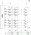
接下来参照图7,示出用于存储器的管芯的结构。对管芯的主机读取请求、GC读取请求、主机写入请求、GC写入请求和其它管理请求通过管芯水平和通道水平的仲裁器在队列中管理和安排。图7描绘NAND装置具有两个通道且每个通道具有两个管芯的示例。在每个管芯中,不同级别的请求可被维持在不同队列中或多个请求被维持在一个队列中。主机读取请求可在被称为主机读取队列的队列中分开,因为只有主机读取请求被允许在管芯暂停期间被伺服。管芯仲裁器从队列中的一个中选择命令,然后通道仲裁器在连接至通道的所有管芯中选择一个管芯的请求。Referring next to FIG. 7, the structure of a die for a memory is shown. Host read requests, GC read requests, host write requests, GC write requests, and other management requests to the die are managed and scheduled in queues by die-level and channel-level arbiters. 7 depicts an example where a NAND device has two channels and each channel has two dies. Within each die, different levels of requests may be maintained in different queues or multiple requests may be maintained in one queue. Host read requests may be split in a queue called a host read queue, since only host read requests are allowed to be served during die pauses. The die arbiter selects the command from one of the queues, and the channel arbiter then selects the request of one die among all the dies connected to the channel.
接下来参照图8,示出在编程暂停-恢复过程中的步骤的流程图80。Referring next to FIG. 8, a
在步骤800中,接收命令请求。一般而言,只有来自非繁忙管芯的请求可在通道仲裁器中被发出。当编程暂停-恢复被涉及时,等待读取请求可当管芯处于暂停准备好或恢复状态但仍然繁忙时被发出。因此,繁忙但可暂停的管芯也应该被认为是仲裁候选。系统可基于暂停阈值确定管芯是否(哪个)可暂停。例如,当状态处于暂停准备好时,暂停阈值可当剩余编程时间大于编程暂停延迟(例如,暂停超出)时被满足。当状态处于恢复时,暂停阈值可当伺服的读取请求的数量小于最大暂停计数且剩余编程时间大于(编程暂停延迟+数据恢复时间)(例如,重复暂停-恢复超出)时被满足。In
在步骤804中,产生暂停请求和恢复请求并将暂停请求和恢复请求插入队列中。为了有效减少主机读取延迟,在一个实施例中,只有主机读取请求被允许在管芯暂停期间被伺服。本领域技术人员将理解其它命令请求可适于在此公开的暂停。当调度编程仲裁等待主机读取请求且管芯可暂停时,暂停请求和恢复请求将被生成并被插入对应的管芯的主机读取队列中。在示例中,暂停请求被插入队列的前端,且恢复请求被插入由当前主机请求队列长度指示的位置中。In
在暂停期间待被伺服的读取请求的数量可被确定为限额=最大暂停计数-伺服的读取请求的数量。如果队列长度大于或等于限额+1,待被插入到队列中的恢复请求的位置可被计算为位置=限额+1,否则位置将是队列的尾部。The number of read requests to be served during a pause may be determined as quota=maximum pause count-number of read requests to be served. If the queue length is greater than or equal to quota+1, the position of the resume request to be inserted into the queue can be calculated as position=quota+1, otherwise the position will be the tail of the queue.
在步骤806中,执行命令。由于在管芯暂停后只有来自管芯的主机读取队列的请求被伺服,所以暂停请求一被插入队列中管芯仲裁器就锁定主机读取队列(这意味着管芯仲裁器仅从该队列中选择请求)。当稍后恢复请求被成功发出时,管芯仲裁器解锁队列。通道仲裁器可授予最高优先权以暂停请求和恢复请求。如果多个管芯具有暂停/恢复请求,通道仲裁器可在这些管芯中遵循循环仲裁方案。In
在步骤808中,解暂停管芯并计算剩余编程时间。当状态进入暂停准备好状态时,剩余编程时间被初始化为管芯编程时间,且起始编程时间被记录为最后记录的时间标记以进一步使用。当状态进入恢复状态时,当前时间标记被记录为最后记录的时间标记。当状态进入暂停状态时,如果状态从暂停准备好转变为暂停,则剩余编程时间通过剩余编程时间=剩余编程时间-(当前时间标记-最后记录的时间标记)来计算。如果状态从恢复转变为暂停,则当(当前时间标记-最后记录的时间标记)小于或等于数据恢复时间时剩余编程时间通过剩余编程时间=剩余编程时间来计算。否则,当(当前时间标记-最后记录的时间标记)但与数据恢复时间时,剩余编程时间通过剩余编程时间-(当前时间标记-最后记录的时间标记)来计算。In
还可执行管芯状态轮询。控制器控制管芯状态变化以为了确定用于下一个待被发出的请求的可利用资源。由于高的轮询费用,控制器当需要时轮询管芯状态。在正常的管芯编程中,由于管芯编程在管芯编程时间后将被完成,所以控制器设置管芯编程时间后的暂停时间并在暂停时间轮询管芯状态。然而,如果当在管芯编程时间后暂停时间发生时编程被暂停中断,则控制器不应轮询管芯状态,而当恢复请求被成功发出时新的暂停时间应该在剩余编程时间后发送。Die status polling can also be performed. The controller controls the die state changes in order to determine the available resources for the next request to be issued. Due to the high polling cost, the controller polls the die status when needed. In normal die programming, since the die programming will be completed after the die programming time, the controller sets a pause time after the die programming time and polls the die status at the pause time. However, if programming is interrupted by a pause when the pause time occurs after the die programming time, the controller should not poll the die status, and a new pause time should be sent after the remaining programming time when a resume request is issued successfully.
当意味着管芯在剩余编程时间期间被再次暂停的重复的暂停-恢复发生时,控制器不应在被先前恢复请求设置的剩余编程时间暂停时间后轮询管芯状态。因此,最后的恢复请求被记录。当暂停时间发生时,控制器在其开始轮询管芯状态之前检查状态是否被恢复及暂停时间是否由最后的恢复请求引起。When repeated suspend-resume occurs, meaning the die is suspended again during the remaining programming time, the controller should not poll the die status after the remaining programming time suspend time set by the previous resume request. Therefore, the last recovery request is recorded. When a suspend time occurs, the controller checks whether the state was restored and whether the suspend time was caused by the last resume request before it starts polling the die status.
利用随机读取和随机写入组合主机通信量的不同OP和不同百分比进行实验,比较具有编程暂停-恢复的持续混合工作负载性能与在没有用于配备有3D TLC单稳态编程的NAND装置的编程暂停-恢复的情况下的性能。使用不同最大暂停计数值1、5和10。Experiments were conducted with different OPs and different percentages of random read and random write combined host traffic, comparing sustained mixed workload performance with program suspend-resume with that in the absence of programming for NAND devices equipped with 3D TLC monostable programming. Programming suspend-resume performance. Use different maximum pause count values of 1, 5, and 10.
尽管为了清楚说明的目的已经相当详细地描述了前述实施例,但本发明不限于提供的细节。存在许多实施本发明的可选方法。公开的实施例是说明性的且不是限制性的。Although the foregoing embodiments have been described in considerable detail for purposes of clarity of illustration, the invention is not limited to the details provided. There are many alternative ways of implementing the present invention. The disclosed embodiments are illustrative and not restrictive.
Claims (13)
Applications Claiming Priority (2)
| Application Number | Priority Date | Filing Date | Title |
|---|---|---|---|
| US201562150700P | 2015-04-21 | 2015-04-21 | |
| US62/150,700 | 2015-04-21 |
Publications (2)
| Publication Number | Publication Date |
|---|---|
| CN106067321A CN106067321A (en) | 2016-11-02 |
| CN106067321B true CN106067321B (en) | 2020-09-15 |
Family
ID=57147713
Family Applications (1)
| Application Number | Title | Priority Date | Filing Date |
|---|---|---|---|
| CN201610252450.9A Active CN106067321B (en) | 2015-04-21 | 2016-04-21 | Controller suitable for memory programming pause-resume |
Country Status (2)
| Country | Link |
|---|---|
| US (1) | US10540115B2 (en) |
| CN (1) | CN106067321B (en) |
Families Citing this family (32)
| Publication number | Priority date | Publication date | Assignee | Title |
|---|---|---|---|---|
| US10558398B2 (en) * | 2016-07-29 | 2020-02-11 | Seagate Technology Llc | Reducing read latency |
| CN106547492B (en) | 2016-12-08 | 2018-03-20 | 北京得瑞领新科技有限公司 | The operational order dispatching method and device of a kind of NAND flash memory equipment |
| US10558392B2 (en) | 2017-06-30 | 2020-02-11 | Seagate Technology Llc | Enhancing quality of service of a storage device |
| KR102386811B1 (en) * | 2017-07-18 | 2022-04-15 | 에스케이하이닉스 주식회사 | Memory system and operating method thereof |
| JP2019029045A (en) | 2017-07-26 | 2019-02-21 | 東芝メモリ株式会社 | Semiconductor storage device |
| KR102631353B1 (en) | 2017-08-17 | 2024-01-31 | 삼성전자주식회사 | Nonvolatile memory device and operating method of the same |
| KR102447465B1 (en) * | 2017-09-08 | 2022-09-27 | 삼성전자주식회사 | A storage device that temporarily suspends internal operations to provide a short read response time for read requests from the host. |
| JP2019057147A (en) * | 2017-09-21 | 2019-04-11 | 東芝メモリ株式会社 | Memory system |
| KR102420161B1 (en) | 2017-12-01 | 2022-07-12 | 삼성전자주식회사 | Memory controller and control method thereof |
| KR102570454B1 (en) * | 2018-04-06 | 2023-08-25 | 에스케이하이닉스 주식회사 | Semiconductor memory device and method of the same |
| US10817217B2 (en) * | 2018-06-28 | 2020-10-27 | Seagate Technology Llc | Data storage system with improved time-to-ready |
| KR20200015190A (en) * | 2018-08-03 | 2020-02-12 | 에스케이하이닉스 주식회사 | Data Storage Device and Operation Method Thereof, Storage System Having the Same |
| US10739839B2 (en) | 2018-09-24 | 2020-08-11 | Western Digital Technologies, Inc. | Efficient power management stand-by modes for multiple dies in a storage device |
| KR102725221B1 (en) | 2018-11-16 | 2024-11-01 | 삼성전자주식회사 | Storage device throttling amount of communicated data depending on suspension frequency of operation |
| KR102680273B1 (en) * | 2019-02-12 | 2024-07-01 | 삼성전자주식회사 | A method for controlling a suspend mode and a memory controller including the same |
| US11614890B2 (en) * | 2019-07-30 | 2023-03-28 | Micron Technology, Inc. | Handling of host-initiated requests in memory sub-systems |
| KR102711411B1 (en) * | 2019-09-06 | 2024-09-30 | 에스케이하이닉스 주식회사 | Storage device and operating method thereof |
| KR102861554B1 (en) * | 2019-12-19 | 2025-09-18 | 에스케이하이닉스 주식회사 | Semiconductor memory device, controller and operating methods thereof |
| KR20220137120A (en) * | 2020-03-10 | 2022-10-11 | 마이크론 테크놀로지, 인크 | Method, system and readable storage medium for managing queues in a memory subsystem |
| JP2021174564A (en) * | 2020-04-24 | 2021-11-01 | キオクシア株式会社 | Semiconductor storage device |
| KR102761995B1 (en) * | 2020-05-27 | 2025-02-05 | 에스케이하이닉스 주식회사 | Storage device and operating method thereof |
| US11494316B2 (en) * | 2020-08-24 | 2022-11-08 | Advanced Micro Devices, Inc. | Memory controller with a plurality of command sub-queues and corresponding arbiters |
| US11923016B2 (en) * | 2020-09-25 | 2024-03-05 | Intel Corporation | Progressive program suspend resume |
| US11789748B2 (en) | 2020-10-05 | 2023-10-17 | SK Hynix Inc. | Firmware parameters optimizing systems and methods |
| KR102866029B1 (en) * | 2020-11-27 | 2025-09-26 | 에스케이하이닉스 주식회사 | Memory system and operating method of memory system |
| JP2022092965A (en) * | 2020-12-11 | 2022-06-23 | キオクシア株式会社 | Memory system |
| WO2022165786A1 (en) * | 2021-02-07 | 2022-08-11 | Yangtze Memory Technologies Co., Ltd. | Peak power management for multi-die operations |
| US12131064B2 (en) * | 2021-04-27 | 2024-10-29 | Sk Hynix Nand Product Solutions Corp. | Dynamic program suspend disable for random write SSD workload |
| KR20220165563A (en) * | 2021-06-08 | 2022-12-15 | 에스케이하이닉스 주식회사 | Memory controller and operating method thereof |
| US11748027B2 (en) * | 2021-12-30 | 2023-09-05 | Western Digital Technologies, Inc. | Storage system and method for avoiding clustering of reads during a program suspend |
| JP2024000230A (en) * | 2022-06-20 | 2024-01-05 | 富士通株式会社 | multi die package |
| US12159676B2 (en) * | 2022-08-18 | 2024-12-03 | Yangtze Memory Technologies Co., Ltd. | Memory device and read operation during suspension of program operation thereof |
Citations (2)
| Publication number | Priority date | Publication date | Assignee | Title |
|---|---|---|---|---|
| CN101038789A (en) * | 2006-03-16 | 2007-09-19 | 三星电子株式会社 | Non-volatile phase-change memory device and associated program-suspend-read operation |
| CN102483951A (en) * | 2009-08-28 | 2012-05-30 | 微软公司 | Interruptible nand flash memory |
Family Cites Families (11)
| Publication number | Priority date | Publication date | Assignee | Title |
|---|---|---|---|---|
| US6907502B2 (en) * | 2002-10-03 | 2005-06-14 | International Business Machines Corporation | Method for moving snoop pushes to the front of a request queue |
| US9021158B2 (en) * | 2009-09-09 | 2015-04-28 | SanDisk Technologies, Inc. | Program suspend/resume for memory |
| US8972627B2 (en) * | 2009-09-09 | 2015-03-03 | Fusion-Io, Inc. | Apparatus, system, and method for managing operations for data storage media |
| US8856611B2 (en) * | 2012-08-04 | 2014-10-07 | Lsi Corporation | Soft-decision compensation for flash channel variation |
| US9329986B2 (en) * | 2012-09-10 | 2016-05-03 | Sandisk Technologies Inc. | Peak current management in multi-die non-volatile memory devices |
| US9032177B2 (en) * | 2012-12-04 | 2015-05-12 | HGST Netherlands B.V. | Host read command return reordering based on time estimation of flash read command completion |
| US9779038B2 (en) * | 2013-01-31 | 2017-10-03 | Apple Inc. | Efficient suspend-resume operation in memory devices |
| US9436634B2 (en) * | 2013-03-14 | 2016-09-06 | Seagate Technology Llc | Enhanced queue management |
| US9007841B1 (en) | 2013-10-24 | 2015-04-14 | Western Digital Technologies, Inc. | Programming scheme for improved voltage distribution in solid-state memory |
| US9753653B2 (en) * | 2015-04-14 | 2017-09-05 | Sandisk Technologies Llc | High-priority NAND operations management |
| US10402120B2 (en) * | 2016-07-15 | 2019-09-03 | Advanced Micro Devices, Inc. | Memory controller arbiter with streak and read/write transaction management |
-
2016
- 2016-04-21 CN CN201610252450.9A patent/CN106067321B/en active Active
- 2016-04-21 US US15/135,270 patent/US10540115B2/en active Active
Patent Citations (2)
| Publication number | Priority date | Publication date | Assignee | Title |
|---|---|---|---|---|
| CN101038789A (en) * | 2006-03-16 | 2007-09-19 | 三星电子株式会社 | Non-volatile phase-change memory device and associated program-suspend-read operation |
| CN102483951A (en) * | 2009-08-28 | 2012-05-30 | 微软公司 | Interruptible nand flash memory |
Also Published As
| Publication number | Publication date |
|---|---|
| US20160313946A1 (en) | 2016-10-27 |
| CN106067321A (en) | 2016-11-02 |
| US10540115B2 (en) | 2020-01-21 |
Similar Documents
| Publication | Publication Date | Title |
|---|---|---|
| CN106067321B (en) | Controller suitable for memory programming pause-resume | |
| CN109801669B (en) | Memory system with soft read suspension scheme and method of operating the same | |
| CN110895449B (en) | Apparatus and method for managing valid data in a memory system | |
| CN109426449B (en) | Memory system and method of operation | |
| US20110191525A1 (en) | Flash memory storage device, controller thereof, and data programming method thereof | |
| CN106372004B (en) | Programmable protocol independent BAR memory for SSD controller | |
| US11775389B2 (en) | Deferred error-correction parity calculations | |
| CN106920575B (en) | Data storage device and method of operation thereof | |
| CN110750380B (en) | Memory system with parity cache scheme and method of operation | |
| CN110275796A (en) | Memory system with hybrid decoding scheme and method of operation | |
| CN106372011B (en) | High-performance host queue monitor for PCIE SSD controllers | |
| CN112306394A (en) | Method and storage device for improving QOS latency | |
| US11526439B2 (en) | Storage device and operating method thereof | |
| CN113939797B (en) | Lock management for memory subsystems | |
| CN111435291A (en) | Apparatus and method for erasing programmed data in a block of non-volatile memory | |
| CN106445749A (en) | Reduction of maximum latency using dynamic self-tuning for redundant array of independent disks | |
| CN107544925A (en) | Accumulator system and the method for accelerating boot time | |
| CN112948280A (en) | Storage device, method of operating the same, and method of managing data in the storage device | |
| CN107633862A (en) | Memory system and method of operation thereof | |
| CN110277124A (en) | Memory system with hybrid decoding scheme and method of operation | |
| CN110895447A (en) | Controller and how to operate it | |
| CN116107767A (en) | Controller including multiprocessor and method of operation thereof | |
| CN107977283A (en) | Accumulator system and its operating method with LDPC decoder | |
| US10127984B2 (en) | Method for operating storage device determining wordlines for writing user data depending on reuse period | |
| KR102695482B1 (en) | Data storage device and operating method thereof |
Legal Events
| Date | Code | Title | Description |
|---|---|---|---|
| C06 | Publication | ||
| PB01 | Publication | ||
| SE01 | Entry into force of request for substantive examination | ||
| SE01 | Entry into force of request for substantive examination | ||
| GR01 | Patent grant | ||
| GR01 | Patent grant |