CN103748696A - Method of processing a semiconductor structure - Google Patents
Method of processing a semiconductor structure Download PDFInfo
- Publication number
- CN103748696A CN103748696A CN201280041603.5A CN201280041603A CN103748696A CN 103748696 A CN103748696 A CN 103748696A CN 201280041603 A CN201280041603 A CN 201280041603A CN 103748696 A CN103748696 A CN 103748696A
- Authority
- CN
- China
- Prior art keywords
- substrate
- wafer
- light emitting
- bonding
- semiconductor structure
- Prior art date
- Legal status (The legal status is an assumption and is not a legal conclusion. Google has not performed a legal analysis and makes no representation as to the accuracy of the status listed.)
- Granted
Links
Images


Classifications
-
- H—ELECTRICITY
- H10—SEMICONDUCTOR DEVICES; ELECTRIC SOLID-STATE DEVICES NOT OTHERWISE PROVIDED FOR
- H10H—INORGANIC LIGHT-EMITTING SEMICONDUCTOR DEVICES HAVING POTENTIAL BARRIERS
- H10H20/00—Individual inorganic light-emitting semiconductor devices having potential barriers, e.g. light-emitting diodes [LED]
- H10H20/01—Manufacture or treatment
- H10H20/011—Manufacture or treatment of bodies, e.g. forming semiconductor layers
- H10H20/013—Manufacture or treatment of bodies, e.g. forming semiconductor layers having light-emitting regions comprising only Group III-V materials
- H10H20/0137—Manufacture or treatment of bodies, e.g. forming semiconductor layers having light-emitting regions comprising only Group III-V materials the light-emitting regions comprising nitride materials
-
- H—ELECTRICITY
- H10—SEMICONDUCTOR DEVICES; ELECTRIC SOLID-STATE DEVICES NOT OTHERWISE PROVIDED FOR
- H10H—INORGANIC LIGHT-EMITTING SEMICONDUCTOR DEVICES HAVING POTENTIAL BARRIERS
- H10H20/00—Individual inorganic light-emitting semiconductor devices having potential barriers, e.g. light-emitting diodes [LED]
- H10H20/80—Constructional details
- H10H20/85—Packages
- H10H20/851—Wavelength conversion means
- H10H20/8515—Wavelength conversion means not being in contact with the bodies
-
- H—ELECTRICITY
- H10—SEMICONDUCTOR DEVICES; ELECTRIC SOLID-STATE DEVICES NOT OTHERWISE PROVIDED FOR
- H10H—INORGANIC LIGHT-EMITTING SEMICONDUCTOR DEVICES HAVING POTENTIAL BARRIERS
- H10H20/00—Individual inorganic light-emitting semiconductor devices having potential barriers, e.g. light-emitting diodes [LED]
- H10H20/01—Manufacture or treatment
- H10H20/011—Manufacture or treatment of bodies, e.g. forming semiconductor layers
- H10H20/018—Bonding of wafers
-
- H—ELECTRICITY
- H10—SEMICONDUCTOR DEVICES; ELECTRIC SOLID-STATE DEVICES NOT OTHERWISE PROVIDED FOR
- H10H—INORGANIC LIGHT-EMITTING SEMICONDUCTOR DEVICES HAVING POTENTIAL BARRIERS
- H10H20/00—Individual inorganic light-emitting semiconductor devices having potential barriers, e.g. light-emitting diodes [LED]
- H10H20/80—Constructional details
- H10H20/81—Bodies
- H10H20/819—Bodies characterised by their shape, e.g. curved or truncated substrates
-
- H—ELECTRICITY
- H10—SEMICONDUCTOR DEVICES; ELECTRIC SOLID-STATE DEVICES NOT OTHERWISE PROVIDED FOR
- H10H—INORGANIC LIGHT-EMITTING SEMICONDUCTOR DEVICES HAVING POTENTIAL BARRIERS
- H10H20/00—Individual inorganic light-emitting semiconductor devices having potential barriers, e.g. light-emitting diodes [LED]
- H10H20/80—Constructional details
- H10H20/81—Bodies
- H10H20/822—Materials of the light-emitting regions
- H10H20/824—Materials of the light-emitting regions comprising only Group III-V materials, e.g. GaP
- H10H20/825—Materials of the light-emitting regions comprising only Group III-V materials, e.g. GaP containing nitrogen, e.g. GaN
-
- H—ELECTRICITY
- H10—SEMICONDUCTOR DEVICES; ELECTRIC SOLID-STATE DEVICES NOT OTHERWISE PROVIDED FOR
- H10H—INORGANIC LIGHT-EMITTING SEMICONDUCTOR DEVICES HAVING POTENTIAL BARRIERS
- H10H20/00—Individual inorganic light-emitting semiconductor devices having potential barriers, e.g. light-emitting diodes [LED]
- H10H20/80—Constructional details
- H10H20/83—Electrodes
-
- H—ELECTRICITY
- H10—SEMICONDUCTOR DEVICES; ELECTRIC SOLID-STATE DEVICES NOT OTHERWISE PROVIDED FOR
- H10H—INORGANIC LIGHT-EMITTING SEMICONDUCTOR DEVICES HAVING POTENTIAL BARRIERS
- H10H20/00—Individual inorganic light-emitting semiconductor devices having potential barriers, e.g. light-emitting diodes [LED]
- H10H20/80—Constructional details
- H10H20/84—Coatings, e.g. passivation layers or antireflective coatings
- H10H20/841—Reflective coatings, e.g. dielectric Bragg reflectors
-
- H—ELECTRICITY
- H10—SEMICONDUCTOR DEVICES; ELECTRIC SOLID-STATE DEVICES NOT OTHERWISE PROVIDED FOR
- H10H—INORGANIC LIGHT-EMITTING SEMICONDUCTOR DEVICES HAVING POTENTIAL BARRIERS
- H10H20/00—Individual inorganic light-emitting semiconductor devices having potential barriers, e.g. light-emitting diodes [LED]
- H10H20/80—Constructional details
- H10H20/85—Packages
- H10H20/851—Wavelength conversion means
- H10H20/8511—Wavelength conversion means characterised by their material, e.g. binder
- H10H20/8512—Wavelength conversion materials
-
- H—ELECTRICITY
- H10—SEMICONDUCTOR DEVICES; ELECTRIC SOLID-STATE DEVICES NOT OTHERWISE PROVIDED FOR
- H10P—GENERIC PROCESSES OR APPARATUS FOR THE MANUFACTURE OR TREATMENT OF DEVICES COVERED BY CLASS H10
- H10P74/00—Testing or measuring during manufacture or treatment of wafers, substrates or devices
- H10P74/23—Testing or measuring during manufacture or treatment of wafers, substrates or devices characterised by multiple measurements, corrections, marking or sorting processes
- H10P74/235—Testing or measuring during manufacture or treatment of wafers, substrates or devices characterised by multiple measurements, corrections, marking or sorting processes comprising optical enhancement of defects or not-directly-visible states
-
- H—ELECTRICITY
- H10—SEMICONDUCTOR DEVICES; ELECTRIC SOLID-STATE DEVICES NOT OTHERWISE PROVIDED FOR
- H10H—INORGANIC LIGHT-EMITTING SEMICONDUCTOR DEVICES HAVING POTENTIAL BARRIERS
- H10H20/00—Individual inorganic light-emitting semiconductor devices having potential barriers, e.g. light-emitting diodes [LED]
- H10H20/01—Manufacture or treatment
- H10H20/036—Manufacture or treatment of packages
- H10H20/0361—Manufacture or treatment of packages of wavelength conversion means
-
- H—ELECTRICITY
- H10—SEMICONDUCTOR DEVICES; ELECTRIC SOLID-STATE DEVICES NOT OTHERWISE PROVIDED FOR
- H10H—INORGANIC LIGHT-EMITTING SEMICONDUCTOR DEVICES HAVING POTENTIAL BARRIERS
- H10H20/00—Individual inorganic light-emitting semiconductor devices having potential barriers, e.g. light-emitting diodes [LED]
- H10H20/80—Constructional details
- H10H20/85—Packages
- H10H20/851—Wavelength conversion means
- H10H20/8511—Wavelength conversion means characterised by their material, e.g. binder
Landscapes
- Led Devices (AREA)
- Led Device Packages (AREA)
- Optical Filters (AREA)
- Laser Beam Processing (AREA)
Abstract
根据本发明各实施例的方法包括提供包括生长在生长衬底上的半导体结构的晶片,该半导体结构包括夹在n型区域和p型区域之间的III族氮化物发光层。该晶片结合到第二衬底。该生长衬底被移除。在将该晶片结合到该第二衬底之后,该晶片被加工成多个发光器件。The method according to various embodiments of the present invention includes providing a wafer comprising a semiconductor structure grown on a growth substrate, the semiconductor structure including a group III nitride light-emitting layer sandwiched between n-type and p-type regions. The wafer is bonded to a second substrate. The growth substrate is removed. After bonding the wafer to the second substrate, the wafer is fabricated into a plurality of light-emitting devices.
Description
背景技术。 background technology .
技术领域 technical field
本发明涉及将包括半导体结构的晶片结合到衬底,随后将该晶片加工为多个发光器件。 The present invention involves bonding a wafer comprising semiconductor structures to a substrate and subsequently processing the wafer into a plurality of light emitting devices.
相关技术的描述 Description of related technologies
包括发光二极管(LED)、谐振腔发光二极管(RCLED)、垂直腔激光二极管(VCSEL)和边缘发射激光器的半导体发光器件属于当前可获得的最高效光源。在能够跨过可见光谱操作的高亮度发光器件的制造中当前感兴趣的材料系统包括III-V族半导体,特别是也称为III族氮化物材料的镓、铝、铟和氮的二元、三元和四元合金。典型地,通过金属有机物化学气相沉积(MOCVD)、分子束外延(MBE)或其它外延技术,在蓝宝石、碳化硅、III族氮化物或其它合适衬底上外延生长不同组成和掺杂剂浓度的半导体层的叠层来制作III族氮化物发光器件。该叠层经常包括在衬底上形成的掺杂有例如Si的一个或多个n型层,在该一个或多个n型层上形成的有源区域中的一个或多个发光层,以及在该有源区域上形成的掺杂有例如Mg的一个或多个p型层。电接触在n和p型区域上形成。 Semiconductor light emitting devices including light emitting diodes (LEDs), resonant cavity light emitting diodes (RCLEDs), vertical cavity laser diodes (VCSELs) and edge emitting lasers are among the most efficient light sources currently available. Materials systems of current interest in the fabrication of high-brightness light-emitting devices capable of operating across the visible spectrum include III-V semiconductors, in particular binary, aluminum, indium, and nitrogen compounds of gallium, aluminum, indium, and nitrogen, also known as III-nitride materials. Ternary and quaternary alloys. Typically, different compositions and dopant concentrations are epitaxially grown on sapphire, silicon carbide, III-nitride, or other suitable substrates by metal-organic chemical vapor deposition (MOCVD), molecular beam epitaxy (MBE), or other epitaxy techniques. A stack of semiconductor layers is used to fabricate III-nitride light-emitting devices. The stack often includes one or more n-type layers doped with, for example, Si, formed on a substrate, one or more light-emitting layers in the active region formed on the one or more n-type layers, and One or more p-type layers doped with eg Mg are formed on the active region. Electrical contacts are formed on the n- and p-type regions.
随着发射蓝色或紫外光的高效LED的发展,制作这样的LED变得可行,该LED对由LED发射的初级光的一部分进行磷光体转换而生成白光。磷光体将初级光的一部分转换成更长波长的次级光。未转换的初级光可以与次级光组合以产生白光。 With the development of highly efficient LEDs that emit blue or ultraviolet light, it has become feasible to fabricate LEDs that phosphor convert a portion of the primary light emitted by the LED to generate white light. The phosphor converts a portion of the primary light into longer wavelength secondary light. Unconverted primary light can be combined with secondary light to produce white light.
图13图示了在US7,553,683中更详细描述的形成磷光体转换发光器件的方法100。首先制作波长转换材料片(sheet)(步骤102)。可以使用例如分散在诸如玻璃的无机材料中的磷光体或其它类似发光材料来制作波长转换材料片。在坩埚中加热磷光体和粉末化玻璃的非常均匀的混合物。在玻璃混合物熔化之后,熔融物在炉内被均匀化,随后被倾倒在板上并且被允许硬化成平坦的片。一旦波长转换材料片被硬化,该片被分离成许多单独元件(步骤104)。单独波长转换元件经调整大小(sized)以被安装在LED管芯上。随后提供半导体发光器件管芯(步骤106)。LED管芯可以是安装的管芯,例如,该管芯安装在反射器杯或载具中。可替换地,LED管芯可以是未安装的。波长转换元件随后结合到LED管芯(步骤108)。
Figure 13 illustrates a
发明内容 Contents of the invention
本发明的目的是提供一种在将半导体结构结合到第二衬底之后将该半导体结构加工成各发光器件的方法。在结合后的加工可以允许在结合期间使用更高的温度。 It is an object of the present invention to provide a method of processing a semiconductor structure into light emitting devices after bonding the semiconductor structure to a second substrate. Post-bonding processing may allow higher temperatures to be used during bonding.
根据本发明各实施例的方法包括:提供包括生长在生长衬底上的半导体结构的晶片,该半导体结构包括夹在n型区域和p型区域之间的发光层。该晶片结合到第二衬底。该生长衬底被移除。在将该晶片结合到该第二衬底之后,该晶片被加工成多个发光器件。 Methods according to embodiments of the invention include providing a wafer comprising a semiconductor structure grown on a growth substrate, the semiconductor structure comprising a light emitting layer sandwiched between an n-type region and a p-type region. The wafer is bonded to a second substrate. The growth substrate is removed. After bonding the wafer to the second substrate, the wafer is processed into a plurality of light emitting devices.
由于晶片是在结合到第二衬底之后而非之前被加工成各发光器件,更高的结合温度以及需要更高的加工温度的衬底材料可以被使用,这可以改善发光器件的性能。 Since the wafer is processed into light emitting devices after bonding to the second substrate rather than before, higher bonding temperatures and substrate materials that require higher processing temperatures can be used, which can improve the performance of the light emitting devices.
附图说明 Description of drawings
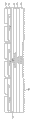
图1图示生长在生长衬底上的包括n型区域、发光区域和p型区域的半导体结构。 FIG. 1 illustrates a semiconductor structure including an n-type region, a light emitting region and a p-type region grown on a growth substrate.
图2图示结合到处置部(handle)的图1的结构。 Figure 2 illustrates the structure of Figure 1 incorporated into a handle.
图3图示在移除生长衬底并且结合到第二衬底之后图2的结构。 Figure 3 illustrates the structure of Figure 2 after removal of the growth substrate and bonding to a second substrate.
图4图示在移除处置部之后图3的结构。 FIG. 4 illustrates the structure of FIG. 3 after removal of the treatment portion.
图5图示在结合到第二衬底并且移除生长衬底之后图1的结构。 Figure 5 illustrates the structure of Figure 1 after bonding to a second substrate and removal of the growth substrate.
图6图示在形成金属p接触,蚀刻形成台面以及形成金属n接触之后图4所图示结构的一部分。 6 illustrates a portion of the structure illustrated in FIG. 4 after forming a metal p-contact, etching to form a mesa, and forming a metal n-contact.
图7图示在形成金属n接触,蚀刻形成台面以及形成金属p接触之后图5所图示结构的一部分。 7 illustrates a portion of the structure illustrated in FIG. 5 after forming a metal n-contact, etching to form a mesa, and forming a metal p-contact.
图8图示在调节衬底中波长转换材料的数量之后器件的晶片的一部分。 Figure 8 illustrates a portion of a wafer of devices after adjusting the amount of wavelength converting material in the substrate.
图9图示在纹理化衬底之后器件的晶片的一部分。 Figure 9 illustrates a portion of a wafer of devices after texturing the substrate.
图10图示在切割器件的晶片之后的三个器件。 Figure 10 illustrates three devices after dicing the wafer of devices.
图11图示在形成电介质涂层之后的三个器件。 Figure 11 illustrates the three devices after forming the dielectric coating.
图12图示在移除过量电介质涂层之后的三个器件。 Figure 12 illustrates the three devices after removal of excess dielectric coating.
图13图示用于形成磷光体转换LED的现有技术方法。 Figure 13 illustrates a prior art method for forming phosphor converted LEDs.
具体实施方式 Detailed ways
在图13的方法中,在半导体材料晶片生长,加工成器件以及切割成单独器件芯片之后,波长转换玻璃构件被结合到LED管芯。在加工和切割完成之后,LED芯片典型地只能够在最多~400℃的温度加工。在更高温度加工LED会导致LED性能特性劣化以及在加工期间沉积的层的潜在分层或破裂。许多合适玻璃层需要远超过400℃的结合温度。结果,图13的加工温度约束(~400℃)限制了可被使用的材料的选择。另外,与具有更高结合温度的合适玻璃相比,具有更低结合温度的合适玻璃趋于具有更强光学吸收,特别是在更短光学波长处。结合了更低温度结合玻璃的器件由此可能招致性能损失。 In the method of FIG. 13, the wavelength converting glass member is bonded to the LED die after the wafer of semiconductor material is grown, processed into devices, and diced into individual device chips. After processing and dicing are complete, LED chips can typically only be processed at temperatures up to ~400°C. Processing LEDs at higher temperatures can lead to degradation of LED performance characteristics and potential delamination or cracking of deposited layers during processing. Many suitable glass layers require bonding temperatures well in excess of 400°C. As a result, the processing temperature constraints of Figure 13 (~400°C) limit the choice of materials that can be used. Additionally, suitable glasses with lower bonding temperatures tend to have stronger optical absorption, especially at shorter optical wavelengths, than suitable glasses with higher bonding temperatures. Devices incorporating lower temperature bonding glasses may thus incur performance losses.
在本发明各实施例中,在生长半导体结构之后并且在半导体结构被进一步加工(例如通过形成金属接触)之前,在晶片级工艺中将包括布置在n型区域和p型区域之间的发光区域的半导体结构结合到高指数衬底。半导体结构随后被加工成诸如发光二极管的发光器件。如此处使用,“晶片”是指在其被分割成更小结构之前的结构,诸如用于许多发光器件的半导体材料生长在其上的生长衬底。尽管在下述示例中半导体发光器件为发射蓝光或UV光的III族氮化物LED,可以使用LED之外的半导体发光器件,诸如由其它材料系统(诸如其它III-V族材料、III族磷化物、III族砷化物、II-VI族材料、ZnO或Si基材料)制成的激光二极管和半导体发光器件。 In various embodiments of the invention, after growing the semiconductor structure and before the semiconductor structure is further processed (for example by forming metal contacts), a light emitting region arranged between the n-type region and the p-type region will be included in the wafer level process The semiconductor structure is bonded to a high index substrate. The semiconductor structure is subsequently processed into a light emitting device such as a light emitting diode. As used herein, "wafer" refers to a structure before it is divided into smaller structures, such as a growth substrate on which semiconductor material for many light emitting devices is grown. Although in the following examples the semiconductor light-emitting device is a III-nitride LED emitting blue or UV light, semiconductor light-emitting devices other than LEDs may be used, such as those made of other material systems (such as other III-V materials, III-phosphides, Laser diodes and semiconductor light-emitting devices made of group III arsenides, II-VI materials, ZnO or Si-based materials).
图1图示生长在生长衬底11上的半导体结构13。衬底11可以是任何合适衬底,诸如,例如蓝宝石、SiC、Si、GaN或复合衬底。半导体结构包括夹在n型区域12和p型区域16之间的发光或有源区域14。n型区域12可以首先生长并且可以包括不同组成和掺杂剂浓度的多个层,所述多个层例如包括诸如缓冲层或成核层的准备层,和/或设计成促进生长衬底移除的层(其可以是n型或非故意掺杂的),以及针对发光区域高效发射光所期望的具体光学或电学属性设计的n或甚至p型器件层。发光或有源区域14生长在n型区域12上。合适发光区域的示例包括单个厚或薄的发光层,或者包括由各垒层分隔的多个薄或厚的发光层的多量子阱发光区域。p型区域16可以随后生长在发光区域14上。与n型区域12类似,p型区域16可以包括不同组成、厚度和掺杂剂浓度的多个层(包括非故意掺杂的层或n型层)。器件中所有半导体材料的总厚度在一些实施例中小于10µm并且在一些实施例中小于6µm。在一些实施例中,半导体材料可以在生长之后可选地在200℃和800℃之间退火。
FIG. 1 illustrates a
在一些实施例中,图1中生长的结构附连到处置部20,如图2所图示。在移除生长衬底11期间,处置部20机械地支持半导体结构13。处置部20可以是例如蓝宝石、硅或任何其它合适材料。在一些实施例中,例如通过在热和压力下将处置部20和半导体结构13压在一起或者通过阳极结合(其中处置部20和半导体结构13在热和静电场下被压在一起),处置部20直接结合到半导体结构13。在一些实施例中,处置部20通过一种或多种结合层18被结合到半导体结构13。结合层可以仅仅形成于处置部20上,仅仅形成于半导体结构13上,或者形成于处置部20和半导体结构13二者上。结合层可以是任何合适材料,诸如,例如一种或多种硅氧化物。在形成结合层之后,处置部20和半导体结构13在热和压力下或者在热和静电场下被压在一起。在附连处置部20之后,通过任何适合于生长衬底材料的技术(包括例如激光剥离、蚀刻或机械技术)移除生长衬底11。
In some embodiments, the grown structure in FIG. 1 is attached to a
在图3图示的结构中,生长衬底已经从图2的结构移除,从而露出首先生长的层,此示例中n型区域12。可选的光学阻抗匹配层22可以形成于n型区域12上。光学阻抗匹配层22增强从半导体结构的提取,而不要求粗糙化半导体结构的表面。光学阻抗匹配层22可以是例如由包括蒸发和溅射的任何合适技术形成的抗反射叠层。在一些实施例中,n型区域12被粗糙化。在n型区域12被粗糙化的实施例中,使用柔性结合层23,该柔性结合层流动以填充粗糙化表面中的间隙,使得可以形成充分没有孔洞的结合。
In the structure illustrated in FIG. 3 , the growth substrate has been removed from the structure of FIG. 2 , exposing the first grown layer, in this example the n-
一种或多种结合层23形成于可选的光学阻抗匹配层22(如果存在)上或形成于n型区域12上。结合层23经常为高折射率(例如,在一些实施例中至少1.5)的低光学吸收层。结合层23可以形成于光学阻抗匹配层22上(或者层22不存在时,形成于半导体结构13上),形成于衬底24上,或者形成于这二者上。用于结合层23的合适材料的示例包括:III-V族半导体,其包括但不限于砷化镓、氮化镓、磷化镓和磷化铟镓;II-VI族半导体,其包括但不限于硒化镉、硫化镉、碲化镉、硫化锌、硒化锌和碲化锌;IV族半导体和化合物,其包括但不限于锗、硅和碳化硅;有机半导体,氧化物,金属氧化物,以及稀土氧化物,其包括但不限于铝、锑、砷、铋、硼、镉、铈、铬、钴、铜、镓、锗、铟、铟、铟锡、铅、锂、钼、钕、镍、铌、磷、钾、硅、钠、碲、铊、钛、钨、锌、或锆的氧化物或氮化物;卤氧化物,诸如氧氯化铋;氟化物、氯化物和溴化物,其包括但不限于钙、铅、镁、钾、钠和锌的氟化物、氯化物和溴化物;金属,其包括但不限于铟、镁、锡和锌;钇铝石榴石(YAG),磷化合物,砷化合物,锑化合物,氮化合物,高指数有机化合物;以及它们的混合物或合金。一个或多个结合层23可以通过包括下述的任何合适方法来应用:蒸发、溅射、化学气相沉积、滴涂、印刷、喷涂、旋涂或刮涂。高指数结合材料可以以流体形式沉积,并且可以保持流体一直到连接的时刻,或者在连接的时刻可以部分地固化或凝胶化,或者可以是固体,该固体在加热时粘性增加以实现容易的连接。高指数结合材料可以反应以形成可介于从凝胶化状态变化到硬树脂的固化的结合。
One or more bonding layers 23 are formed on optional optical impedance matching layer 22 (if present) or on n-
半导体结构经由结合层23结合到衬底24。衬底24可以是透明的高折射率材料,诸如预形成为衬底晶片随后结合到半导体结构13的玻璃。上述玻璃的折射率在一些实施例中可以在1.5至2.2的范围内或更高,与GaN的折射率(2.4)紧密匹配。用于衬底24的合适材料包括但不限于电绝缘材料、非半导体材料、玻璃料(frit
glass),合适的高折射率玻璃,诸如氯化铅,溴化铅,氟化钾,氟化锌,铝、锑、铋、硼、铅、锂、磷、钾、硅、钠、碲、铊、钨或锌的氧化物,或者其任何混合物。高折射率玻璃也包括诸如下述的材料:肖特(Schott)玻璃LaSFN35,LaF10,NZK7,NLAF21,LaSFN18,SF59或LaSF3;或者Ohara玻璃SLAH51或SLAM60,或者其混合物;例如,诸如(Ge,As,Sb,Ga)(S,Se,Te,F,Cl,I,Br)硫族化物和硫族卤化物玻璃的玻璃。在一些实施例中,衬底24可以包括下述较低指数材料或由其形成:诸如玻璃,镁氟化物以及聚合物。诸如硅树脂或硅氧烷的高和低指数树脂均可以从诸如日本东京信越化学工业有限公司的制造商获得。硅氧烷骨干的侧链可以被调整以改变硅树脂的折射率。
The semiconductor structure is bonded to a
基本上没有传统有机物基粘合剂(诸如环氧树脂)的玻璃趋于具有更高折射率,这是因为有机物粘合剂趋于具有低的折射率。这些有机物基粘合剂在短波长光和提升温度的组合下也趋于退化,从而将LED的最高操作温度限制到~150℃。因此,在一些实施例中,衬底24为不含有机物的材料,这可以允许LED的更高效操作和/或在更高温度操作。
Glasses substantially free of traditional organic-based binders such as epoxies tend to have a higher index of refraction because organic binders tend to have low indices of refraction. These organic-based adhesives also tend to degrade under the combination of short-wavelength light and elevated temperature, thereby limiting the maximum operating temperature of the LED to ~150°C. Thus, in some embodiments,
在一些实施例中,衬底24为任何一种上述材料的基质,一种或多种发光材料结合到该基质内,所述发光材料将由发光区域发射的波长的光转换为其它波长。由发光区域发射并且入射在波长转换材料上的光的所有或仅仅部分可以被波长转换材料转换。由发光区域发射的未被转换的光可以是最终光谱的一部分,不过不需要如此。常见组合的示例包括发射蓝光的LED与发射黄光的波长转换材料组合,发射蓝光的LED与发射绿光和红光波长转换材料组合,发射UV的LED与发射蓝光和黄光的波长转换材料组合,以及发射UV的LED与发射蓝光、绿光和红光的波长转换材料组合。发射其它颜色光的波长转换材料可以被添加以调节从器件发射的光谱。波长转换材料可以是传统磷光体颗粒、有机半导体、II-VI或III-V族半导体、II-VI或III-V族半导体量子点或纳米晶、染料、聚合物、或者诸如GaN的发光的材料。如果衬底24包括传统磷光体颗粒,在一些实施例中衬底24足够厚以容纳典型地具有大约5微米至大约50微米的尺寸的颗粒。可以使用包括下述的任何合适磷光体:石榴石基磷光体,诸如Y3Al5O12:Ce(YAG)、Lu3Al5O12:Ce(LuAG)、Y3Al5-xGaxO12:Ce(YAlGaG)、(Ba1-xSrx)SiO3:Eu(BOSE);以及氮化物基磷光体,诸如(Ca,Sr)AlSiN3:Eu和(Ca,Sr,Ba)2Si5N8:Eu。
In some embodiments,
在一些实施例中,衬底24为陶瓷,该陶瓷可以是波长转换的。陶瓷衬底24可以例如通过下述形成:烧结诸如任何一种上文所列磷光体的磷光体颗粒,或者烧结其它材料,诸如Al2O3,ZrO2,SiC,AlON,SiON,AlSiON,诸如钛酸钡、钛酸钙、钛酸锶、锆钛酸铅的钛酸盐,或者未激活的YAG。陶瓷衬底24可以是透明、半透明或散射的。
In some embodiments,
在一些实施例中,半导体结构13通过下述结合到衬底24:在提升的温度将这两个结构压在一起。例如,结合温度可以在一些实施例中高达800℃,在一些实施例中大于400℃,在一些实施例中大于500℃,以及在一些实施例中介于500和800℃。在一些实施例中,在结合的时间也可以应用小于90kN的压力。在一些实施例中,也可以在半导体结构13和衬底24之间应用电势差。
In some embodiments,
如图4所图示,在结合到衬底24之后,例如通过蚀刻、机械分离、激光剥离或者任何其它合适技术移除处置部20。例如通过蚀刻移除在移除处置部20之后余留的任何结合材料18。在图4所图示的结构中,半导体结构通过n型区域12的表面结合到衬底24。p型区域16的顶表面露出。
As illustrated in FIG. 4, after bonding to the
作为图2、3和4所图示工艺的可替换方案,图1的结构可以被加工成图5所图示的结构。在图5所图示的结构中,可选的光学阻抗匹配层22形成于图1所图示半导体结构的p型区域16的顶表面上。一种或多种结合层23形成,随后半导体结构结合到衬底24,如上文参考图3所描述。生长衬底11随后被移除,如上文所描述。在图5所图示的结构中,半导体结构13经由p型区域16结合到衬底24。n型区域12的顶表面露出。
As an alternative to the processes illustrated in FIGS. 2 , 3 and 4 , the structure of FIG. 1 may be processed into the structure illustrated in FIG. 5 . In the structure illustrated in FIG. 5 , an optional optical
图6图示在形成电连接到n和p型区域的金属接触之后图4的结构。首先形成p接触33。图示的p接触33包括两个金属层32和34。金属32可以通过例如蒸发或溅射被沉积,随后通过包括例如蚀刻或剥离的标准光刻操作被图案化。金属32可以是诸如与p型III族氮化物材料形成欧姆接触的反射金属,例如银。金属32也可以是过渡金属和银的多层叠层。过渡金属例如可以是镍。金属32在一些实施例中厚度介于100Å和2000Å,在一些实施例中厚度介于500Å和1700Å,以及在一些实施例中厚度介于1000Å和1600Å。该结构可以可选地在沉积金属32之后被退火。
FIG. 6 illustrates the structure of FIG. 4 after forming metal contacts electrically connected to the n and p-type regions. First the p-
可选的第二p接触金属34可以通过例如蒸发或溅射被沉积在p接触金属32上,随后诸如通过例如蚀刻或剥离的标准光刻操作被图案化。金属34诸如可以是最小程度地与银反应的任何导电材料,例如钛和钨的合金。这种合金可以或者被部分地氮化,被全部氮化,或者根本不氮化。金属34可替换地可以是铬、铂或硅,或者可以是针对附着到周围层或针对阻挡金属32扩散而优化的任何上述材料的多层叠层。金属34可以在一些实施例中厚度介于1000Å和10000Å,在一些实施例中厚度介于2000Å和8000Å,以及在一些实施例中厚度介于2000Å和7000Å。
An optional second p-
该结构随后通过标准光刻操作被图案化,并且通过例如反应离子蚀刻(RIE)或感应耦合等离子体(ICP)蚀刻被蚀刻,其中在反应离子蚀刻中,化学反应等离子体被用于移除半导体材料,其中感应耦合等离子体蚀刻为通过RF供电的磁场生成等离子体的RIE工艺。在一些实施例中,图案由用于图案化p接触金属34的光刻掩模确定。在这些实施例中,该蚀刻可以在p接触金属34的蚀刻之后在单个操作中被执行。在一些区域中,p型区域16的整个厚度以及发光区域14的整个厚度被移除,显露n型区域12的表面。
The structure is then patterned by standard photolithographic operations and etched by, for example, reactive ion etching (RIE) or inductively coupled plasma (ICP) etching, in which a chemically reactive plasma is used to remove semiconductor materials, where inductively coupled plasma etching is an RIE process in which plasma is generated by an RF-powered magnetic field. In some embodiments, the pattern is determined by a photolithographic mask used to pattern p-
金属n接触36形成于通过蚀刻掉p型区域和发光区域而露出的n型区域12的那部分上。n接触36可以是任何合适金属,包括铝或者包括铝、钛-钨合金、铜和金的金属的多层叠层。在n接触36为多层叠层的实施例中,第一金属(即毗邻n型区域12的金属)可以被选择以与GaN形成欧姆接触并且对于蓝光和白光是反射的。这种第一层可以是例如铝。n接触36可以通过任何合适工艺沉积,该工艺包括例如溅射、蒸发、电镀或这些工艺的组合。
A metal n-
电介质38可以例如通过等离子体增强化学气相沉积(PECVD)、化学气相沉积(CVD)或蒸发沉积在该结构上。电介质38电学隔离n接触36和p接触33。电介质38由标准光刻操作进行图案化,并且由ICP蚀刻或RIE蚀刻以露出n接触36和p接触33。电介质38可以是任何合适电介质,包括硅氮化物、硅氧化物以及硅氮氧化物。在一些实施例中,电介质38是反射叠层。电介质38可以在形成n接触36之前或之后形成。
结合垫40a和40b可以形成于n和p接触以及电介质38上,从而将n和p接触重新分配到大导电垫,所述大导电垫适合于诸如结合到例如PC板的另一结构。结合垫典型地为金属,但是可以是任何合适的导电材料。结合垫40a通过p接触33电连接到p型区域16。结合垫40b通过n接触36电连接到n型区域12。结合垫40可以是例如通过溅射或者通过溅射和电镀的组合而沉积的Cu或者包括例如Ti、TiW、Cu、Ni和Au的多层金属叠层。结合垫40a和40b可以通过间隙电隔离,如图6和7所图示,或者通过诸如上文参考电介质38所描述的材料的固体电介质电隔离。
图7图示在形成电连接到n和p型区域的金属接触之后图5的结构。图7与图6相反:n接触36可以首先形成,随后n型区域12和发光区域14的一部分被蚀刻掉以显露p型区域16,随后p接触33形成于p型区域16的露出部分上。n和p接触36和33通过电介质层38电隔离。结合垫40a和40b分别电连接到p和n接触33和36。n和p接触金属36和33、电介质38以及结合垫40可以是按照与上文参考图6所描述相同的方式形成的相同材料。
FIG. 7 illustrates the structure of FIG. 5 after forming metal contacts electrically connected to the n- and p-type regions. FIG. 7 is the opposite of FIG. 6 : n-
尽管在图6和7的每一个中仅仅图示一个器件,应理解,上文图示和描述的加工步骤典型地发生在包括多个器件的晶片上。在一些实施例中,n接触和/或p接触可以被分配,使得蚀刻形成图6中的多个n接触开口和图7中的多个p接触开口。在图8、9、10、11和12中图示多个器件,所述器件可以或者是图6所图示的器件,或者是图7所图示的器件。在图8、9、10、11和12中,半导体结构13可以或者如图6所图示使p型区域16位于顶部,或者如图7所图示使n型区域12位于顶部。类似地,在图8、9、10、11和12中被示为结构31的金属接触33和36以及电介质38可以形成为图6所图示的配置或者图7所图示的配置。
Although only one device is illustrated in each of Figures 6 and 7, it should be understood that the processing steps illustrated and described above typically occur on a wafer comprising multiple devices. In some embodiments, n-contacts and/or p-contacts may be allocated such that the etch forms multiple n-contact openings in FIG. 6 and multiple p-contact openings in FIG. 7 . A number of devices are illustrated in FIGS. 8 , 9 , 10 , 11 and 12 , which may be either the devices illustrated in FIG. 6 or the devices illustrated in FIG. 7 . In FIGS. 8 , 9 , 10 , 11 and 12 ,
在晶片上的单独器件完成之后,整个晶片可以被测试。在衬底24为波长转换的实施例中,每个LED的颜色可以在图8所图示的可选步骤中被调谐。图8的结构包括包含半导体结构13的晶片的一部分。三个器件42、44和46被图示。基于测试结果,通过基于测试结果调整每个器件上存在的波长转换材料的数量,可以进一步调谐晶片上每个单独LED管芯的颜色。如果在整个晶片测试该器件不产生期望波长谱,波长转换衬底24的厚度被改变,例如通过局部地沉积附加波长转换材料(器件42和46),或者通过利用消融、蚀刻或溶解而局部地移除某些波长转换材料(器件44)。如果需要,有可能数次测试并且重新调节波长转换材料厚度,直至产生期望的波长光谱。响应于由LED产生的光,光转换层的厚度被控制,从而得到高度可重现的颜色。此外,由于光转换层的厚度响应于由LED产生的特定波长而改变,因此可以容纳由遍布晶片的各LED产生的光的波长变化。因此,更少的LED会由于产生具有不期望的波长谱的光而被抛弃。
After the individual devices on the wafer are completed, the entire wafer can be tested. In embodiments where
在图9中,通过粗糙化或图案化而可选地纹理化与接触一个或多个结合层23的表面相对的衬底24的表面48,这可以提高光提取。纹理化可以通过包括例如蚀刻、激光消融的任何合适技术来执行,或者通过将另一结构(诸如光栅或比如菲涅耳透镜的透镜)层压到衬底24上来执行。
In FIG. 9, the
在图10中,保护性剥离聚合物层52沉积在晶片顶部上,随后器件的晶片被切割为各器件芯片。每个器件芯片可以包括单个发光二极管或者发光二极管群组。由于半导体结构13和衬底24一起被切片(dice),衬底不比器件宽,如图10、11和12图示。可以例如通过传统锯切,通过使用193nm、248nm或355nm光的激光消融,或者通过喷水切割来执行该切割。也可以经由划片和机械折断的组合来执行该切割,该划片例如通过传统锯切,通过使用193nm、248nm或355nm光的激光消融,或通过喷水切割来执行。
In Figure 10, a protective
在图11中,可选的反射涂层形成于器件的顶部56和各侧面54之上。例如,反射涂层形成于保护性剥离聚合物层52之上以及聚合物层52、结合垫40a和40b、结构31、半导体结构13、结合层23和衬底24的各侧面上。该涂层可以是例如由包括蒸发的任何合适技术形成的高反射电介质叠层。侧面涂层54减小或消除从每个器件的侧面的光泄漏。当保护性剥离聚合物层52被移除以露出结合垫40时,图12中器件的顶部56上的涂层被移除。器件现在可以通过焊接而附连到任何合适结构,例如附连到PC板。
In FIG. 11, an optional reflective coating is formed over the top 56 and
尽管上述示例图示倒装芯片器件,有可能使用其它器件几何,包括光通过接触从器件被提取的具有透明接触的器件以及具有顶部和底部接触的垂直器件。在垂直器件中,部分的衬底24可以被移除或者不形成从而容纳例如具有金属填充的通孔的接触。可替换地,垂直器件中的接触可以形成于导电衬底24上。在上文图示的示例中,大多数光朝向衬底24被引导离开半导体结构。在诸如具有透明接触的器件或者垂直器件的一些实施例中,大多数光可以朝向与衬底24相对的半导体结构的表面被引导离开半导体结构。在这种实施例中,诸如反射金属的反射结合层可以被使用,并且衬底24可以是透明或不透明的。金属结合层也可以用作接触。
Although the above examples illustrate flip-chip devices, it is possible to use other device geometries, including devices with transparent contacts where light is extracted from the device through the contacts, and vertical devices with top and bottom contacts. In vertical devices, portions of the
与传统加工相比,本发明各实施例可以提供优势。在图6和7图示的加工(即形成金属接触和电介质层)之前,半导体结构13可以在高达~800℃的温度被加工。由于在图6和7图示的加工之前半导体结构13被结合到衬底24,衬底24可以由高熔点的高折射率材料制成。高熔点的高折射率玻璃经常具有比较低熔点的高折射率玻璃低的光学吸收。使用具有较低光学吸收的衬底24可以改善器件的性能。另外,高温度软化点玻璃通常具有更低的热膨胀系数(CTE),与较低熔点玻璃的CTE相比更好地匹配III族氮化物半导体结构13的CTE。得到的结构因此可以具有减少的内建应力,这可以减少结构由于在温度循环期间积累的应力而破裂或分层的趋势,尽管半导体结构13在高温结合到衬底24。
Embodiments of the present invention may provide advantages over conventional processing. The
已经详细地描述了本发明,但是本领域技术人员将理解,考虑到本公开内容,可以对本发明进行各调整而不背离此处所述发明构思的精神。因此,不意图将本发明的范围限制在所图示和描述的特定实施例。 The present invention has been described in detail, but those skilled in the art will appreciate that, in view of the present disclosure, various modifications can be made therein without departing from the spirit of the inventive concepts described herein. Therefore, it is not intended that the scope of the invention be limited to the specific embodiments shown and described.
Claims (20)
Applications Claiming Priority (3)
| Application Number | Priority Date | Filing Date | Title |
|---|---|---|---|
| US201161527634P | 2011-08-26 | 2011-08-26 | |
| US61/527634 | 2011-08-26 | ||
| PCT/IB2012/054225 WO2013030718A1 (en) | 2011-08-26 | 2012-08-21 | Method of processing a semiconductor structure |
Publications (2)
| Publication Number | Publication Date |
|---|---|
| CN103748696A true CN103748696A (en) | 2014-04-23 |
| CN103748696B CN103748696B (en) | 2018-06-22 |
Family
ID=47148861
Family Applications (1)
| Application Number | Title | Priority Date | Filing Date |
|---|---|---|---|
| CN201280041603.5A Active CN103748696B (en) | 2011-08-26 | 2012-08-21 | The method for processing semiconductor structure |
Country Status (7)
| Country | Link |
|---|---|
| US (1) | US10056531B2 (en) |
| EP (1) | EP2748864B1 (en) |
| JP (2) | JP6305337B2 (en) |
| KR (2) | KR101965265B1 (en) |
| CN (1) | CN103748696B (en) |
| TW (2) | TWI583029B (en) |
| WO (1) | WO2013030718A1 (en) |
Cited By (3)
| Publication number | Priority date | Publication date | Assignee | Title |
|---|---|---|---|---|
| CN108630718A (en) * | 2017-03-21 | 2018-10-09 | 晶元光电股份有限公司 | Light emitting element |
| CN109461805A (en) * | 2018-03-07 | 2019-03-12 | 普瑞光电股份有限公司 | Automobile LED light source with the glass lens being located on the glass change-over panel comprising fluorophor |
| CN110581201A (en) * | 2018-06-08 | 2019-12-17 | 信越半导体株式会社 | Light-emitting component and method for manufacturing the light-emitting component |
Families Citing this family (13)
| Publication number | Priority date | Publication date | Assignee | Title |
|---|---|---|---|---|
| EP2732478B1 (en) | 2011-07-15 | 2018-09-19 | Lumileds Holding B.V. | Method of bonding a semiconductor device to a support substrate |
| WO2013118072A2 (en) | 2012-02-10 | 2013-08-15 | Koninklijke Philips N.V. | Wavelength converted light emitting device |
| KR20170069240A (en) * | 2014-10-01 | 2017-06-20 | 코닌클리케 필립스 엔.브이. | Light source with tunable emission spectrum |
| US10217914B2 (en) | 2015-05-27 | 2019-02-26 | Samsung Electronics Co., Ltd. | Semiconductor light emitting device |
| JP2017220479A (en) * | 2016-06-03 | 2017-12-14 | 株式会社ディスコ | Method for manufacturing light-emitting diode chip |
| JP2017224726A (en) * | 2016-06-15 | 2017-12-21 | 株式会社ディスコ | Method for manufacturing light-emitting diode chip |
| JP2017224728A (en) * | 2016-06-15 | 2017-12-21 | 株式会社ディスコ | Method for manufacturing light-emitting diode chip |
| JP2018014425A (en) * | 2016-07-21 | 2018-01-25 | 株式会社ディスコ | Method for manufacturing light-emitting diode chip |
| US10559727B2 (en) * | 2017-07-25 | 2020-02-11 | Shenzhen China Star Optoelectronics Semiconductor Display Technology Co., Ltd. | Manufacturing method of colorful Micro-LED, display modlue and terminals |
| DE112018007310T5 (en) | 2018-03-21 | 2020-12-17 | OSRAM Opto Semiconductors Gesellschaft mit beschränkter Haftung | OPTOELECTRONIC DEVICE HAVING A LUMINOUS PLATE AND METHOD OF MANUFACTURING THE OPTOELECTRONIC DEVICE |
| CN110544641A (en) * | 2018-05-28 | 2019-12-06 | 山东浪潮华光光电子股份有限公司 | Test method of light emitting diode chip |
| JP7108196B2 (en) | 2019-12-26 | 2022-07-28 | 日亜化学工業株式会社 | Light-emitting device, method for manufacturing wavelength conversion member, and method for manufacturing light-emitting device |
| KR20210123064A (en) * | 2020-04-02 | 2021-10-13 | 웨이브로드 주식회사 | Method of manufacturing a iii-nitride semiconducter device |
Citations (5)
| Publication number | Priority date | Publication date | Assignee | Title |
|---|---|---|---|---|
| EP0611131A1 (en) * | 1993-02-10 | 1994-08-17 | Sharp Kabushiki Kaisha | A method for producing a light-emitting diode having a transparent substrate |
| WO2005091390A1 (en) * | 2004-03-18 | 2005-09-29 | Showa Denko K.K. | Group iii nitride semiconductor light-emitting device and producing method thereof |
| JP2007016171A (en) * | 2005-07-08 | 2007-01-25 | Sharp Corp | Wavelength conversion member, light emitting device, and method of manufacturing wavelength conversion member |
| DE102008039790A1 (en) * | 2008-08-26 | 2010-03-04 | Osram Opto Semiconductors Gmbh | Optoelectronic component i.e. LED, for use as headlight in motor vehicle, has connecting terminals provided for supplying charge carriers to partial layers of layer sequence, where terminals are arranged at main side of layer sequence |
| WO2010110204A1 (en) * | 2009-03-27 | 2010-09-30 | コニカミノルタオプト株式会社 | Phosphor member, method for producing phosphor member, and lighting device |
Family Cites Families (22)
| Publication number | Priority date | Publication date | Assignee | Title |
|---|---|---|---|---|
| JP2002344029A (en) | 2001-05-17 | 2002-11-29 | Rohm Co Ltd | How to adjust the color tone of light emitting diodes |
| TWI231054B (en) * | 2003-03-13 | 2005-04-11 | Showa Denko Kk | Light-emitting diode and its manufacturing method |
| WO2005050748A1 (en) | 2003-11-19 | 2005-06-02 | Nichia Corporation | Semiconductor device and method for manufacturing same |
| JP4594708B2 (en) * | 2003-12-05 | 2010-12-08 | 昭和電工株式会社 | LIGHT EMITTING DIODE AND ITS MANUFACTURING METHOD, LIGHT EMITTING DIODE LAMP |
| JP2005259912A (en) | 2004-03-10 | 2005-09-22 | Shin Etsu Handotai Co Ltd | Manufacturing method of light emitting element |
| JP4116587B2 (en) * | 2004-04-13 | 2008-07-09 | 浜松ホトニクス株式会社 | Semiconductor light emitting device and manufacturing method thereof |
| JP4857596B2 (en) * | 2004-06-24 | 2012-01-18 | 豊田合成株式会社 | Method for manufacturing light emitting device |
| US7560294B2 (en) | 2004-06-07 | 2009-07-14 | Toyoda Gosei Co., Ltd. | Light emitting element and method of making same |
| US7553683B2 (en) | 2004-06-09 | 2009-06-30 | Philips Lumiled Lighting Co., Llc | Method of forming pre-fabricated wavelength converting elements for semiconductor light emitting devices |
| US20080070380A1 (en) * | 2004-06-11 | 2008-03-20 | Showda Denko K.K. | Production Method of Compound Semiconductor Device Wafer |
| JP4692059B2 (en) * | 2005-04-25 | 2011-06-01 | パナソニック電工株式会社 | Method for manufacturing light emitting device |
| US7456080B2 (en) * | 2005-12-19 | 2008-11-25 | Corning Incorporated | Semiconductor on glass insulator made using improved ion implantation process |
| JP2008135697A (en) | 2006-10-23 | 2008-06-12 | Rohm Co Ltd | Semiconductor light emitting device |
| US7521862B2 (en) | 2006-11-20 | 2009-04-21 | Philips Lumileds Lighting Co., Llc | Light emitting device including luminescent ceramic and light-scattering material |
| JP2008159628A (en) | 2006-12-20 | 2008-07-10 | Rohm Co Ltd | Semiconductor light-emitting element and manufacturing method of semiconductor light-emitting element |
| US7989236B2 (en) | 2007-12-27 | 2011-08-02 | Toyoda Gosei Co., Ltd. | Method of making phosphor containing glass plate, method of making light emitting device |
| US8877524B2 (en) * | 2008-03-31 | 2014-11-04 | Cree, Inc. | Emission tuning methods and devices fabricated utilizing methods |
| US8236582B2 (en) * | 2008-07-24 | 2012-08-07 | Philips Lumileds Lighting Company, Llc | Controlling edge emission in package-free LED die |
| US10147843B2 (en) | 2008-07-24 | 2018-12-04 | Lumileds Llc | Semiconductor light emitting device including a window layer and a light-directing structure |
| JP2010087292A (en) * | 2008-09-30 | 2010-04-15 | Toyoda Gosei Co Ltd | Light emitting element |
| EP2384073B1 (en) | 2009-01-27 | 2018-02-28 | Mitsubishi Electric Corporation | Transmission apparatus, communication system, and communication method |
| US8581229B2 (en) | 2009-11-23 | 2013-11-12 | Koninklijke Philips N.V. | III-V light emitting device with thin n-type region |
-
2012
- 2012-08-21 US US14/238,477 patent/US10056531B2/en active Active
- 2012-08-21 KR KR1020147007513A patent/KR101965265B1/en active Active
- 2012-08-21 EP EP12784063.5A patent/EP2748864B1/en active Active
- 2012-08-21 KR KR1020197008997A patent/KR102082499B1/en active Active
- 2012-08-21 WO PCT/IB2012/054225 patent/WO2013030718A1/en not_active Ceased
- 2012-08-21 CN CN201280041603.5A patent/CN103748696B/en active Active
- 2012-08-21 JP JP2014526585A patent/JP6305337B2/en active Active
- 2012-08-24 TW TW101130877A patent/TWI583029B/en active
- 2012-08-24 TW TW106103469A patent/TWI635628B/en active
-
2016
- 2016-07-21 JP JP2016142915A patent/JP6294402B2/en active Active
Patent Citations (5)
| Publication number | Priority date | Publication date | Assignee | Title |
|---|---|---|---|---|
| EP0611131A1 (en) * | 1993-02-10 | 1994-08-17 | Sharp Kabushiki Kaisha | A method for producing a light-emitting diode having a transparent substrate |
| WO2005091390A1 (en) * | 2004-03-18 | 2005-09-29 | Showa Denko K.K. | Group iii nitride semiconductor light-emitting device and producing method thereof |
| JP2007016171A (en) * | 2005-07-08 | 2007-01-25 | Sharp Corp | Wavelength conversion member, light emitting device, and method of manufacturing wavelength conversion member |
| DE102008039790A1 (en) * | 2008-08-26 | 2010-03-04 | Osram Opto Semiconductors Gmbh | Optoelectronic component i.e. LED, for use as headlight in motor vehicle, has connecting terminals provided for supplying charge carriers to partial layers of layer sequence, where terminals are arranged at main side of layer sequence |
| WO2010110204A1 (en) * | 2009-03-27 | 2010-09-30 | コニカミノルタオプト株式会社 | Phosphor member, method for producing phosphor member, and lighting device |
Cited By (4)
| Publication number | Priority date | Publication date | Assignee | Title |
|---|---|---|---|---|
| CN108630718A (en) * | 2017-03-21 | 2018-10-09 | 晶元光电股份有限公司 | Light emitting element |
| CN109461805A (en) * | 2018-03-07 | 2019-03-12 | 普瑞光电股份有限公司 | Automobile LED light source with the glass lens being located on the glass change-over panel comprising fluorophor |
| CN109461805B (en) * | 2018-03-07 | 2021-08-10 | 普瑞光电股份有限公司 | Automotive LED light source with glass lens on phosphor-containing glass conversion plate |
| CN110581201A (en) * | 2018-06-08 | 2019-12-17 | 信越半导体株式会社 | Light-emitting component and method for manufacturing the light-emitting component |
Also Published As
| Publication number | Publication date |
|---|---|
| JP2016213490A (en) | 2016-12-15 |
| TWI635628B (en) | 2018-09-11 |
| KR102082499B1 (en) | 2020-02-27 |
| JP6305337B2 (en) | 2018-04-04 |
| JP2014525674A (en) | 2014-09-29 |
| TW201318229A (en) | 2013-05-01 |
| JP6294402B2 (en) | 2018-03-14 |
| KR20190038671A (en) | 2019-04-08 |
| EP2748864B1 (en) | 2020-02-05 |
| US10056531B2 (en) | 2018-08-21 |
| WO2013030718A1 (en) | 2013-03-07 |
| KR101965265B1 (en) | 2019-04-04 |
| TW201717436A (en) | 2017-05-16 |
| EP2748864A1 (en) | 2014-07-02 |
| CN103748696B (en) | 2018-06-22 |
| KR20140053361A (en) | 2014-05-07 |
| TWI583029B (en) | 2017-05-11 |
| US20140179029A1 (en) | 2014-06-26 |
Similar Documents
| Publication | Publication Date | Title |
|---|---|---|
| CN103748696B (en) | The method for processing semiconductor structure | |
| JP6419077B2 (en) | Wavelength conversion light emitting device | |
| JP6462029B2 (en) | Method for bonding a substrate to a semiconductor light emitting device | |
| US9484513B2 (en) | Semiconductor light emitting device with thick metal layers | |
| US9362471B2 (en) | Semiconductor light emitting device with thick metal layers | |
| WO2013084103A1 (en) | Semiconductor light emitting device with thick metal layers |
Legal Events
| Date | Code | Title | Description |
|---|---|---|---|
| C06 | Publication | ||
| PB01 | Publication | ||
| C10 | Entry into substantive examination | ||
| SE01 | Entry into force of request for substantive examination | ||
| TA01 | Transfer of patent application right |
Effective date of registration: 20180326 Address after: Holland Schiphol Applicant after: LUMILEDS HOLDING B.V. Address before: Holland Ian Deho Finn Applicant before: Koninkl Philips Electronics NV |
|
| TA01 | Transfer of patent application right | ||
| GR01 | Patent grant | ||
| GR01 | Patent grant |