CN103744567A - Method for manufacturing capacitive touch screen and touch-control layer, and electronic device - Google Patents
Method for manufacturing capacitive touch screen and touch-control layer, and electronic device Download PDFInfo
- Publication number
- CN103744567A CN103744567A CN201410012835.9A CN201410012835A CN103744567A CN 103744567 A CN103744567 A CN 103744567A CN 201410012835 A CN201410012835 A CN 201410012835A CN 103744567 A CN103744567 A CN 103744567A
- Authority
- CN
- China
- Prior art keywords
- conductive inks
- metallic conductive
- line layer
- layer
- inks line
- Prior art date
- Legal status (The legal status is an assumption and is not a legal conclusion. Google has not performed a legal analysis and makes no representation as to the accuracy of the status listed.)
- Pending
Links
- 238000000034 method Methods 0.000 title claims abstract description 29
- 238000004519 manufacturing process Methods 0.000 title abstract description 15
- 239000011521 glass Substances 0.000 claims abstract description 54
- 239000000758 substrate Substances 0.000 claims abstract description 53
- 230000003287 optical effect Effects 0.000 claims abstract description 9
- 239000000976 ink Substances 0.000 claims description 146
- 238000007639 printing Methods 0.000 claims description 36
- 230000008569 process Effects 0.000 claims description 17
- 239000000463 material Substances 0.000 claims description 12
- 238000002360 preparation method Methods 0.000 claims description 7
- 239000002002 slurry Substances 0.000 claims description 7
- 239000007787 solid Substances 0.000 claims description 6
- RYGMFSIKBFXOCR-UHFFFAOYSA-N Copper Chemical compound [Cu] RYGMFSIKBFXOCR-UHFFFAOYSA-N 0.000 claims description 4
- BQCADISMDOOEFD-UHFFFAOYSA-N Silver Chemical compound [Ag] BQCADISMDOOEFD-UHFFFAOYSA-N 0.000 claims description 4
- 229910052802 copper Inorganic materials 0.000 claims description 4
- 239000010949 copper Substances 0.000 claims description 4
- 238000003825 pressing Methods 0.000 claims description 4
- 239000002904 solvent Substances 0.000 claims description 4
- ATJFFYVFTNAWJD-UHFFFAOYSA-N Tin Chemical compound [Sn] ATJFFYVFTNAWJD-UHFFFAOYSA-N 0.000 claims description 3
- 229910002056 binary alloy Inorganic materials 0.000 claims description 3
- 238000004140 cleaning Methods 0.000 claims description 3
- 239000000428 dust Substances 0.000 claims description 3
- 239000000945 filler Substances 0.000 claims description 3
- 239000012530 fluid Substances 0.000 claims description 3
- 239000003292 glue Substances 0.000 claims description 3
- 239000011858 nanopowder Substances 0.000 claims description 3
- 239000002352 surface water Substances 0.000 claims description 3
- 239000010410 layer Substances 0.000 abstract description 158
- 229910052751 metal Inorganic materials 0.000 abstract description 10
- 239000002184 metal Substances 0.000 abstract description 9
- 239000012790 adhesive layer Substances 0.000 abstract 1
- WABPQHHGFIMREM-UHFFFAOYSA-N lead(0) Chemical compound [Pb] WABPQHHGFIMREM-UHFFFAOYSA-N 0.000 abstract 1
- 229920000139 polyethylene terephthalate Polymers 0.000 description 19
- 239000004020 conductor Substances 0.000 description 5
- 230000008901 benefit Effects 0.000 description 4
- 239000003795 chemical substances by application Substances 0.000 description 4
- 230000000694 effects Effects 0.000 description 4
- MRNHPUHPBOKKQT-UHFFFAOYSA-N indium;tin;hydrate Chemical compound O.[In].[Sn] MRNHPUHPBOKKQT-UHFFFAOYSA-N 0.000 description 4
- 239000004973 liquid crystal related substance Substances 0.000 description 4
- 230000035945 sensitivity Effects 0.000 description 4
- 238000001514 detection method Methods 0.000 description 3
- 230000007613 environmental effect Effects 0.000 description 3
- 238000012797 qualification Methods 0.000 description 3
- 229920002799 BoPET Polymers 0.000 description 2
- CDBYLPFSWZWCQE-UHFFFAOYSA-L Sodium Carbonate Chemical class [Na+].[Na+].[O-]C([O-])=O CDBYLPFSWZWCQE-UHFFFAOYSA-L 0.000 description 2
- 230000008859 change Effects 0.000 description 2
- 239000011248 coating agent Substances 0.000 description 2
- 238000000576 coating method Methods 0.000 description 2
- 210000002858 crystal cell Anatomy 0.000 description 2
- 238000011161 development Methods 0.000 description 2
- 238000005516 engineering process Methods 0.000 description 2
- 238000010030 laminating Methods 0.000 description 2
- 239000011159 matrix material Substances 0.000 description 2
- 238000004321 preservation Methods 0.000 description 2
- 238000001771 vacuum deposition Methods 0.000 description 2
- 239000002912 waste gas Substances 0.000 description 2
- 239000002351 wastewater Substances 0.000 description 2
- OKTJSMMVPCPJKN-UHFFFAOYSA-N Carbon Chemical compound [C] OKTJSMMVPCPJKN-UHFFFAOYSA-N 0.000 description 1
- 239000002253 acid Substances 0.000 description 1
- 239000000853 adhesive Substances 0.000 description 1
- 239000000956 alloy Substances 0.000 description 1
- 238000005452 bending Methods 0.000 description 1
- 230000015572 biosynthetic process Effects 0.000 description 1
- 238000004364 calculation method Methods 0.000 description 1
- 239000003990 capacitor Substances 0.000 description 1
- 239000002131 composite material Substances 0.000 description 1
- 239000002322 conducting polymer Substances 0.000 description 1
- 229920001940 conductive polymer Polymers 0.000 description 1
- 238000010276 construction Methods 0.000 description 1
- 230000007812 deficiency Effects 0.000 description 1
- 238000010586 diagram Methods 0.000 description 1
- 238000005265 energy consumption Methods 0.000 description 1
- 238000005530 etching Methods 0.000 description 1
- 229910021389 graphene Inorganic materials 0.000 description 1
- 230000006872 improvement Effects 0.000 description 1
- 230000006698 induction Effects 0.000 description 1
- 239000004615 ingredient Substances 0.000 description 1
- 238000009413 insulation Methods 0.000 description 1
- 239000007769 metal material Substances 0.000 description 1
- 238000012986 modification Methods 0.000 description 1
- 230000004048 modification Effects 0.000 description 1
- 238000005498 polishing Methods 0.000 description 1
- 229920006267 polyester film Polymers 0.000 description 1
- 238000012545 processing Methods 0.000 description 1
- 230000001681 protective effect Effects 0.000 description 1
- 229910001404 rare earth metal oxide Inorganic materials 0.000 description 1
- 238000011160 research Methods 0.000 description 1
- 238000003892 spreading Methods 0.000 description 1
- 230000007480 spreading Effects 0.000 description 1
- 238000004381 surface treatment Methods 0.000 description 1
- 238000002834 transmittance Methods 0.000 description 1
- 229910052727 yttrium Inorganic materials 0.000 description 1
Images


Landscapes
- Position Input By Displaying (AREA)
Abstract
The invention is suitable for the technical field of touch screen structures, and discloses a method for manufacturing a capacitive touch screen and a touch-control layer, and an electronic device. The capacitive touch screen comprises a panel and a screen module, wherein an optical adhesive layer and a BM border layer are arranged between the panel and the screen module; the screen module comprises an upper polarizer, an upper glass substrate, a lower glass substrate, a lower polarizer and a backlight board which are sequentially arranged in a cascade manner from top to bottom, wherein a first metal conductive ink circuit layer is arranged on the panel, a second metal conductive ink circuit layer is arranged in the screen module, or both the first metal conductive ink circuit layer and the second metal conductive ink circuit layer are arranged in the screen module; each of the first metal conductive ink circuit layer and the second metal conductive ink circuit layer comprises a plurality of touch units, and each of the touch units is provided with a lead wire connected with a processor. The capacitive touch screen is sensitive in touch control and high in accuracy degree; the production method for the touch-control layer is simple, low in cost, energy-saving and environment-friendly, and capable of improving the use convenience and reliability of the electronic device with the touch screen.
Description
Technical field
The invention belongs to touch screen structure technical field, relate in particular to the manufacture method of a kind of capacitive touch screen and touch control layer thereof and there is the electronic equipment of this touch-screen.
Background technology
Capacitive touch screen is what to utilize the electric current induction of human body while touching to change to come to touch location.The touch technology of projecting type capacitor panel: projected capacitive touch screen is at one deck ITO(tin indium oxide) etch the ITO conducting wire module of different directions in electro-conductive glass coating.Etched figure in two kinds of modules, can regard X and Y-direction continually varying draw runner as them.Because X, Y framework are at different surfaces, its intersection forms a capacitive node.A draw runner can be treated as drive wire, and it is detection lines that another one draw runner is treated as.When electric current passes through a wire in drive wire, if the extraneous signal that has capacitance variations will cause the variation of capacitive node on another layer conductor so.The variation of detecting capacitance can measure by the electronic loop being attached thereto, then via A/D controller, transfers digital signal to and by computing machine, do calculation process and obtain (X, Y) shaft position, and then reaches the order ground of location.
In traditional capacitive touch screen, the general ITO that adopts is as conductive material, its method of making conductive pattern generally adopts vacuum coating+gold-tinted technique to complete, i.e. general technological process comprises vacuum coating → light blockage coating → exposure → development → etching → stripping etc.Due to the insulation course and the protective seam that generally comprise in touch screen structure between multilayer conductive circuit (containing lead line) and different layers, above-mentioned technique needs repeatedly (generally to want 4~6 times).This has brought series of problems, and as high in equipment investment, workshop area occupied is large, energy consumption is high, and development etch process need to use a large amount of soda acids and is unfavorable for environmental protection.Meanwhile, tin indium oxide is a kind of rare earth oxide, and resource is on the verge of exhaustion, and the conducting film impedance that this material is made is larger, and for the touch-screen of large-size, it touches precision and sensitivity is difficult to reach requirement.
In industry, also having some companies or research institution to deliver ITO(tin indium oxide) equivalent material makes the method for touch-screen, as adopt CNT, metal grill, nano-silver thread, conducting polymer composite etc., but material preparation difficulty or conducting film or conductive pattern are manufactured difficulty, complex process, is difficult to industrialization.
Summary of the invention
The object of the invention is to overcome above-mentioned the deficiencies in the prior art, manufacture method and the electronic equipment of a kind of capacitive touch screen and touch control layer are provided, touch-screen impedance is low, control highly sensitive, the simple environmental protection of manufacturing process, improved and had reliability and the convenience that the electronic equipment of this touch-screen uses.
Technical scheme of the present invention is: a kind of capacitive touch screen, comprise panel and screen module for pressing touch, between described panel and described screen module, be provided with described panel is sticked on to the transparent optical glue-line on described screen module, the surrounding of the one side that described panel is connected with described screen module is also provided with BM frame layer, described screen module comprises the upper polaroid that is cascading and sticks to each other from top to bottom, top glass substrate, lower glass substrate, lower polaroid and backlight, on described panel, be provided with the first metallic conductive inks line layer of one deck for sensing, in described screen module, be provided with the second metallic conductive inks line layer of one deck for sensing, or described the first metallic conductive inks line layer and described the second metallic conductive inks line layer are all arranged in described screen module, in described the first metallic conductive inks line layer and described the second metallic conductive inks line layer, be provided with the touch control unit of polylith for touch control, each described touch control unit is set up in parallel and each described touch control unit is all independently provided with the lead-in wire being connected with processor.
Further, between described panel and described upper polaroid, be also provided with PET thin layer, described PET thin layer upper, be provided with respectively the transparent optical glue-line for pasting with described panel and described upper polaroid below, described the first metallic conductive inks line layer and described the second metallic conductive inks line layer can also be separately positioned on the upper of described PET thin layer, lower two faces, or described the first metallic conductive inks line layer is arranged on the upper of described PET thin layer, any one side in lower two faces, described the second metallic conductive inks line layer is arranged in described screen module.
Particularly, be arranged on described the second metallic conductive inks line layer in described screen module and can be arranged in the upper surface of upper surface, lower surface or described top glass substrate of described upper polaroid or the upper surface of the lower surface of lower glass substrate or lower polaroid, lower surface arbitrarily on a selected face; Or be arranged on described the first metallic conductive inks line layer in described screen module and described the second metallic conductive inks line layer and can be arranged in the upper surface of upper surface, lower surface or described top glass substrate of described upper polaroid or the upper surface of the lower surface of lower glass substrate or lower polaroid, lower surface arbitrarily on selected two faces.
Preferably, described the first metallic conductive inks line layer and described the second metallic conductive inks line layer are the potpourri of a kind of or its binary alloy nano powder in metallic copper, argent, metallic tin and filler, solvent.
Particularly, in described the first metallic conductive inks line layer and described the second metallic conductive inks line layer, be provided with touch-control square, described touch control unit is arranged and is formed by multiple described touch-control squares, described lead-in wire is arranged on the termination of described touch control unit, and the live width of described metallic conductive inks line is 1~5 μ m.
The present invention also provides a kind of electronic equipment, comprises above-mentioned capacitive touch screen.
The present invention also provides a kind of printing process of above-mentioned capacitive touch screen touch control layer, comprises the steps:
Preparation process: the lower surface of described panel or the upper and lower surface of described PET thin layer or described in the upper and lower surface of polaroid or the upper and lower surface of the upper surface of described top glass substrate or the lower surface of described lower glass substrate or described lower polaroid arbitrarily selected two faces as to be printed, then described to be printed that selectes is cleaned with cleaning machine, finally with plasma electric slurry, the surface of described to be printed is processed;
Print steps: the metallic conductive inks material fluid of viscosity glue is passed through to high precision printing equipment, be printed on selected two described to be printed, on described in two to be printed, formed respectively the first metallic conductive inks line layer and the second metallic conductive inks line layer;
Roasting solid step: by print described the first metallic conductive inks line layer and described the second metallic conductive inks line layer two described in to be printed with baking box or continuous tunnel furnace, carry out, described the first metallic conductive inks line layer and described the second metallic conductive inks line layer that form are solidified.
Particularly, in described preparation process, when the surface of described to be printed is processed with plasma electric slurry, printing surface water droplet angle <30 °.
Particularly, in described print steps, printing equipment printing precision requires <1 μ m, and described the first metallic conductive inks line layer forming after printing and the circuit minimum feature of described the second metallic conductive inks line layer are 1~5 μ m.
Particularly, in described roasting solid step, baking temperature is 80 ℃~250 ℃, and baking time is 10min~60min, adopts baking box baking box interior pollution-free, and temperature difference < 5% in baking box; Adopting continuous tunnel furnace curing environment is hundred grades of dust free rooms, and continuous tunnel furnace constant temperature zone temperature difference < 5%.
Capacitive touch screen provided by the invention, by being provided with for the first metallic conductive inks line layer and the screen module of sensing, be provided with the second metallic conductive inks line layer for sensing on panel, or the first metallic conductive inks line layer and the second metallic conductive inks line layer are all arranged in screen module, and in first and second metallic conductive inks line layer, be formed with multiple touch control units that are set up in parallel, for responding to touch information.The circuit fineness of metallic conductive inks aboundresources, formation is high, and impedance is low, has electro-magnetic screen function, and good in anti-interference performance has improved the accuracy of touch-screen touch control.And, in screen module, thering is inter-adhesive sandwich construction, the first metallic conductive inks line layer and the second metallic conductive inks line layer can be arranged on different structural sheets, have improved the kind of touch-screen manufacture and the scope of application.
Adopt the electronic equipment of above-mentioned capacitive touch screen, this capacitive touch screen touch-control precisely, be quick on the draw, circuit is meticulous, meet the requirement that large scale touch-screen and narrow-frame touch panel are produced, and has improved the type kind of the electronic equipment with this touch-screen and the reliability of use.
Adopt the printing process of above-mentioned capacitive touch screen touch control layer, the cost of material is low for the method, typography is simple, can save large number quipments cost, and, promoted the qualification rate of product, also avoid producing waste gas waste water, energy-conserving and environment-protective.
Accompanying drawing explanation
Fig. 1 is the rear view of the capacitive touch screen that provides of the embodiment of the present invention;
Fig. 2 is the schematic diagram of touch control unit in the first metallic conductive inks line layer of providing of the embodiment of the present invention;
Fig. 3 is that the first metallic conductive inks line layer and the second metallic conductive inks line layer that the embodiment of the present invention provides is separately positioned on the diagrammatic cross-section on PET thin layer upper surface and lower surface;
Fig. 4 is that the first metallic conductive inks line layer that the embodiment of the present invention provides is located at PET thin layer upper surface and the second metallic conductive inks line layer is arranged on the diagrammatic cross-section on polaroid lower surface;
Fig. 5 is that the first metallic conductive inks line layer that the embodiment of the present invention provides is arranged on panel lower surface and the second metallic conductive inks line layer is arranged on the diagrammatic cross-section on polaroid lower surface;
Fig. 6 is that the first metallic conductive inks line layer that the embodiment of the present invention provides is arranged on panel lower surface and the second metallic conductive inks line layer is arranged on the diagrammatic cross-section on lower glass substrate lower surface;
Fig. 7 is that the first metallic conductive inks line layer that the embodiment of the present invention provides is arranged on polaroid upper surface and the second metallic conductive inks line layer is arranged on the diagrammatic cross-section on lower polaroid lower surface;
Fig. 8 is that the first metallic conductive inks line layer that the embodiment of the present invention provides is arranged on top glass substrate upper surface and the second metallic conductive inks line layer is arranged on the diagrammatic cross-section on lower glass substrate lower surface;
Fig. 9 is that the first metallic conductive inks line layer that the embodiment of the present invention provides is arranged on lower glass substrate lower surface and the second metallic conductive inks line layer is arranged on the diagrammatic cross-section on lower polaroid lower surface;
Embodiment
In order to make object of the present invention, technical scheme and advantage clearer, below in conjunction with drawings and Examples, the present invention is further elaborated.Should be appreciated that specific embodiment described herein, only in order to explain the present invention, is not intended to limit the present invention.
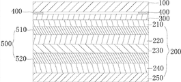
As shown in Figure 1 to Figure 3; a kind of capacitive touch screen 1 that the embodiment of the present invention that the embodiment of the present invention provides provides; comprise panel 100 and screen module 200 for pressing touch; between panel 100 and screen module 200, be provided with transparent optical glue-line 300; transparent optical glue-line 300 can also play panel 100 is sticked on to the effect on screen module 200 in the situation that guaranteeing transmittance; the panel 100 connecting not only can be directly used in touch, can also protect screen module 200.The surrounding of the one side that panel 100 is connected with screen module 200 is also provided with the 400 (abbreviation of BM:Black Matrix of BM frame layer, the Chinese meaning is black matrix"), BM frame layer have the color contrast of raising to, reduce the effect such as light leak, be arranged on the surrounding of panel 100, be used for separating color layer, make the display effect of whole touch-screen better, color is more bright-coloured.Screen module 200 comprises from top to bottom and being cascading, and the upper polaroid 210 sticking to each other, top glass substrate 220, lower glass substrate 230, lower polaroid 240 and backlight 250.Upper polaroid 210 passes through for the polarized light that limits certain orientation, top glass substrate 220 and the bonding preservation liquid crystal of lower glass substrate 230 uniform optical filter, lower glass substrate 230 is with the bonding preservation liquid crystal of top glass substrate 220 and place array line, lower polaroid 240 also passes through for the polarized light that limits certain orientation, backlight 250 is for providing light source, by so stacked combination, form the basic structure of touch-screen.On the lower surface of panel 100, be provided with the first metallic conductive inks line layer 510 of one deck for sensing, in screen module 200, be provided with the second metallic conductive inks line layer 520 of one deck for sensing, or the first metallic conductive inks line layer 510 and the second metallic conductive inks line layer 520 are all arranged in screen module 200, in the first metallic conductive inks line layer 510 and the second metallic conductive inks line layer 520, be provided with the touch control unit 511 of polylith for touch control, each touch control unit 511 is set up in parallel, and each touch control unit 511 is all independently provided with the lead-in wire 512 being connected with processor (not shown).520 points of the first metallic conductive inks line layer 510 and the second metallic conductive inks line layers are arranged, be configured for the sensing module of sensing touch point horizontal ordinate position and ordinate position, acting in conjunction can accurately detect the coordinate figure of touch point, like this, when user's finger touch is during to certain location point on screen, in the first metallic conductive inks line layer 510, understand output signals with the corresponding touch control unit 511 of the second metallic conductive inks line layer 520, when finger moves to another location point, again can be from other touch control unit 511 output signals, 512 signals that each touch control unit 511 can be produced that go between flow to processor, and then realization touches the function that operation is controlled.Particularly, in the present invention, adopt aboundresources, cheap metal or alloy material be main electrically conductive ink as conductive material, be used for making capacitive touch screen 1.Can there is the different structure layer with product in this conductive material, reach the function of touch detection.Metallic conductive inks is a kind of novel conductive material, than traditional ITO(tin indium oxide), possess Low ESR advantage.Lowest surfaces resistance can reach 0.1 Ω/ (Ω/ is face resistance unit) in theory, and possesses electro-magnetic screen function, can reduce signal and disturb; And the sheet resistance of the ITO material of conventional capacitive touch screen 1 is approximately 50~100 Ω/.Impedance is too high, can cause signal source to be disturbed more; Impedance reduces, and also means that producible touch-screen size is larger, and metallic conductive inks even can be used for producing the capacitive touch screen 1 of 100inch.Meanwhile, the precision that can produce circuit is higher, and live width is less.Conventional ITO live width minimum is generally 20~30 μ m, and metallic conductive inks live width minimum can be accomplished 2~5 μ m, can be used to the circuit that production precision is higher, density is larger, as narrow-frame touch panel etc., the range of application of the touch-screen of raising.The sensitivity of touch-screen touch-control and the touch-control accuracy of making are high, have guaranteed the reliability of using.
A kind of capacitive touch screen 1 provided by the invention, adopt aboundresources, cheap metallic conductive inks material to make the first metallic conductive inks line layer 510 and the second metallic conductive inks line layer 520, and according to specific requirement, the first metallic conductive inks line layer 510 and the second metallic conductive inks line layer 520 are arranged in the different structure layer of touch-screen, thereby reach the function of touch detection, realize the touch control of touch-screen.The first metallic conductive inks line layer 510 and the second metallic conductive inks line layer 520 have low-impedance advantage, can be used to the circuit that production precision is higher, density is larger, compared with prior art, compare, it can not only be applied on large-sized screen, and circuit, the live width made are less, can also be used for producing the touch-screen that squeezes frame, improve the kind of touch-screen making and the reliability of use.
Further, as shown in Figure 3 and Figure 4, between panel 100 and upper polaroid 210, be also provided with PET thin layer 600(PET film and have another name called: high temperature resistance polyester film).The above and below of PET thin layer 600 is provided with the transparent optical glue-line 300 for pasting with panel 100 and upper polaroid 210 respectively, when making, can be that the first metallic conductive inks line layer 510 and the second metallic conductive inks line layer 520 are separately positioned on upper and lower two surfaces of PET thin layer 600, also the first metallic conductive inks line layer 510 is arranged in any one side in upper and lower two surfaces of PET thin layer 600, the second metallic conductive inks line layer 520 is arranged in screen module 200.By such setting, the first metallic conductive inks line layer 510 on PET thin layer 600 upper and lower surfaces and the second metallic conductive inks line layer 520, after being subject to touching and pressing, can produce corresponding curent change, and then realize corresponding operation and control function.Meanwhile, PET thin layer 600 can also play the effect of blow-out disc, possesses certain impact resistance, has guaranteed the security that touch-screen is used.
Particularly, as shown in Fig. 3 to Fig. 9, the the second metallic conductive inks line layer 520 being arranged in screen module 200 can be the upper surface that is positioned at polaroid 210, the upper surface of the lower surface of the upper surface of lower surface or top glass substrate 220 or lower glass substrate 230 or lower polaroid 240, on a face of selecting arbitrarily in lower surface, or the first metallic conductive inks line layer 510 and the second metallic conductive inks line layer 520 that are arranged in screen module 200 can be the upper surfaces that lays respectively at polaroid 210, the upper surface of the lower surface of the upper surface of lower surface or top glass substrate 220 or lower glass substrate 230 or lower polaroid 240, on two faces selecting arbitrarily in lower surface, and first the position that arranges of metallic conductive inks line layer 510 and the second metallic conductive inks line layer 520 can exchange.By this setting, any can require to select the first metallic conductive inks line layer 510 and concrete being arranged on two sides of the second metallic conductive inks line layer 520 according to manufacturing, different set-up modes, the function that realizes its touch control operation that equally can be stable, and arrange like this and improved kind that touch-screen makes and the scope of application.
Further, as shown in Fig. 3 to Fig. 9, the first metallic conductive inks line layer 510 and the concrete set-up mode of the second metallic conductive inks line layer 520 are: the first metallic conductive inks line layer 510 and the second metallic conductive inks line layer 520 can be separately positioned on upper and lower two faces of PET thin layer 600; The upper surface that maybe one deck can be arranged to PET thin layer 600, another layer is arranged on upper surface or the lower surface of polaroid 210; Upper surface or the lower surface that maybe one deck can be arranged on to PET thin layer 600, another layer is arranged on the upper surface of top glass substrate 220; Upper surface or the lower surface that maybe one deck can be arranged on to PET thin layer 600, another layer is arranged on the lower surface of lower glass substrate 230; The lower surface that maybe one deck can be arranged on to panel 100, another layer is arranged on the lower surface of polaroid 210; The lower surface that maybe one deck can be arranged on to panel 100, another layer is arranged on the upper surface of top glass substrate 220; The lower surface that maybe one deck can be arranged on to panel 100, another layer is arranged on the lower surface of lower glass substrate 230; The lower surface that maybe one deck can be arranged on to panel 100, another layer is arranged on upper surface or the lower surface of lower polaroid 240; Upper surface or the lower surface that maybe one deck can be arranged on to upper polaroid 210, another layer is arranged on upper surface or the lower surface of lower polaroid 240; The upper surface that maybe one deck can be arranged on to upper polaroid 210, another layer is arranged on the upper surface of top glass substrate 220; Upper surface or the lower surface that maybe one deck can be arranged on to upper polaroid 210, another layer is arranged on the lower surface of lower glass substrate 230; The upper surface that maybe one deck can be arranged on to top glass substrate 220, another layer is arranged on the lower surface of lower glass substrate 230; The upper surface that maybe one deck can be arranged on to top glass substrate 220, another layer is arranged on upper surface or the lower surface of lower polaroid 240; The lower surface that maybe one deck can be arranged on to lower glass substrate 230, another layer is arranged on the lower surface of lower polaroid 240.When actual production is made, can carry out concrete selection according to production requirement.
Preferably, the first metallic conductive inks line layer 510 and the second metallic conductive inks line layer 520 are the potpourri of a kind of or its binary alloy nano powder in metallic copper, argent, metallic tin and filler, solvent.These rich material resources, cheap, by certain technique, be printed on corresponding layer, on each layer, form the circuit of many roundabout bendings or form latticed circuit or form as requested the circuit of other shape, and the circuit fine degree forming is high, can be used to produce the circuit that touch-control accuracy requirement is higher, density is larger, as squeezed frame, high touch-control precision capacitive touch screen 1 etc.Meanwhile, the circuit that adopts metallic conductive inks to make, lowest surfaces resistance can reach 0.1 Ω/ in theory, and possesses electro-magnetic screen function, can reduce signal and disturb, and even can be used for producing the capacitive touch screen 1 of 100inch, applied range.
Particularly, as shown in Figures 2 and 3, in the first metallic conductive inks line layer 510 and the second metallic conductive inks line layer 520, be provided with touch-control square 513, touch control unit 511 is arranged and is formed by multiple touch-control squares 513, and be latticed, the live width of metallic conductive inks line is 1~5 μ m, and lead-in wire 512 is arranged on the termination of touch control unit 511.Metallic conductive inks circuit is to latticed setting, and the live width of circuit is 1~5 μ m, circuit is meticulousr, so just, increase the contact area of metallic conductive inks circuit, then by lead-in wire 512, control signal has been exported, guaranteed the sensitivity that operation is controlled.
The present invention also provides a kind of electronic equipment, comprises above-mentioned capacitive touch screen 1.Capacitive touch screen 1 touch-control is accurate, and reaction sensitivity is high, and the kind of touch-screen is many, can make undersized screen, also can be large-sized screen, can also be made into and squeeze frame screen, improve the kind model of the some subset with this touch-screen and the reliability of use.
The present invention also provides a kind of printing process of capacitive touch screen 1 touch control layer, and printing process comprises the steps:
Preparation process: according to designing requirement, upper at the lower surface of panel 100 or PET thin layer 600, lower surface or upper polaroid 210 upper, the lower surface of the upper surface of lower surface or top glass substrate 220 or lower glass substrate 230 or lower polaroid 240 upper, in lower surface arbitrarily on selected two faces as to be printed, then selected to be printed is cleaned (when metallic conductive inks being printed on the lower surface of panel 100 with cleaning machine, just the lower surface of counter plate 100 first cleans), finally with the surface that plasma electric slurry is treated printing surface, process.
Print steps: the metal grill electrically conductive ink material fluid of viscosity glue is passed through to high precision printing equipment, be printed on selected two to be printed, on two to be printed, form respectively the first metallic conductive inks line layer 510 and the second metallic conductive inks line layer 520, the principal ingredient of metallic conductive inks material is nano-level conducting ink, appearance agent, spreading agent, levelling agent, hardening agent.
Roasting solid step: adopt baking box or continuous tunnel furnace to carry out two to be printed of printing the first metallic conductive inks line layer 510 and the second metallic conductive inks line layer 520, the first metallic conductive inks line layer 510 and the second metallic conductive inks line layer 520 that form are solidified.
Particularly, lead-in wire 512 also needs to be flexible PCB by FPC(FPC, not shown) be electrically connected with processor.Therefore adopt above-mentioned printing process the first metallic conductive inks line layer 510 and the second metallic conductive inks line layer 520 to be printed on respectively the upper of the lower surface of panel 100 or upper polaroid 210, the lower surface of the upper surface of lower surface or top glass substrate 220 or lower glass substrate 230 or lower polaroid 240 upper, after on two faces selecting arbitrarily in lower surface, bind with FPC again, then upper polaroid 210 is fitted on the liquid crystal cell being comprised of upper lower glass substrate 230, and at the lower surface of lower glass substrate 230, stick lower polaroid 240 and form module, finally at laminating panel 100.Any one side in the upper and lower table that the first metallic conductive inks line layer 510 is printed on to PET thin layer 600, when the second metallic conductive inks line layer 520 is printed on the upper surface of top glass substrate 220 or the lower surface of lower glass substrate 230, complete after printing, first upper polaroid 210 is fitted on the liquid crystal cell being combined to form by upper lower glass substrate 230, and stick lower polaroid 240 at the lower surface of lower glass substrate 230, then after laminating PET film, bind with FPC, assemble again backlight, the panel 100 of finally fitting.Concrete number of assembling steps after being completed for printing, can carry out concrete selection according to actual conditions.
Particularly, in preparation process, while processing with the surface that plasma electric slurry is treated printing surface, printing surface water droplet angle <30 °.Like this, while making plasma electric slurry carry out polishing on the surface for the treatment of printing surface (as upper surface of the upper and lower surface of the lower surface of panel 100, upper polaroid 210, top glass substrate 220 etc.), the surface treatment of to be printed can be obtained more evenly, smooth, for next step carries out type metal electrically conductive ink, give security.
Particularly, in print steps, printing equipment printing precision requires <1 μ m, and the first metallic conductive inks line layer 510 forming after printing and the circuit minimum feature of the second metallic conductive inks line layer 520 are 1~5 μ m.By such setting, can be more meticulous in order to the circuit live width of guaranteeing to make by printing, line density is higher, the requirement to conducting wire when squeezing frame, high touch-control precision capacitive touch screen 1 and produce to meet.
Particularly, in roasting solid step, baking temperature is 80 ℃~250 ℃, and baking time is 10min~60min, pollution-free in baking box while adopting baking box baking, and temperature difference < 5% in baking box; Adopting continuous tunnel furnace curing environment is hundred grades of dust free rooms, and continuous tunnel furnace constant temperature zone temperature difference < 5%.Print as requested after metallic conductive inks, need to carry out baking-curing to metallic conductive inks, to form stable metallic conductive inks layer.When baking, according to above-mentioned steps, toast, guarantee the efficiency of baking-curing and solidified the qualification rate of the rear touch control layer forming.
The printing process of capacitive touch screen 1 touch control layer provided by the invention, the first metallic conductive inks line layer 510 and the second metallic conductive inks line layer 520 can directly be printed on to be printed with printing equipment and above then be cured baking, form circuit.This technique can be saved large number quipments cost, material cost, and operation is simple, has reduced production cost, has promoted the qualification rate of product.And, adopt typography to produce, can save the energy, overcome traditional technique needs soda acid equal solvent simultaneously when printing, avoids producing a large amount of waste gas waste water, and the feature of environmental protection is good.The touch-screen making by this printing process is than traditional capacitive touch screen 1, has gentlier, thinner advantage.And, capacitive touch screen 1 module or single-point that this kind of printing process also can be applicable to capacitive touch screen 1 module of Nanometer Copper circuit or capacitive touch screen 1 module of electric ink circuit or Graphene circuit add gesture capacitive touch screen 1 module, applied range.
The foregoing is only preferred embodiment of the present invention, not in order to limit the present invention, all any modifications of doing within the spirit and principles in the present invention, be equal to and replace or improvement etc., within all should being included in protection scope of the present invention.
Claims (10)
1. a capacitive touch screen, comprise panel and screen module for pressing touch, between described panel and described screen module, be provided with described panel is sticked on to the transparent optical glue-line on described screen module, the surrounding of the one side that described panel is connected with described screen module is also provided with BM frame layer, described screen module comprises the upper polaroid that is cascading and sticks to each other from top to bottom, top glass substrate, lower glass substrate, lower polaroid and backlight, it is characterized in that, on described panel, be provided with the first metallic conductive inks line layer of one deck for sensing, in described screen module, be provided with the second metallic conductive inks line layer of one deck for sensing, or described the first metallic conductive inks line layer and described the second metallic conductive inks line layer are all arranged in described screen module, in described the first metallic conductive inks line layer and described the second metallic conductive inks line layer, be provided with the touch control unit of polylith for touch control, each described touch control unit is set up in parallel and each described touch control unit is all independently provided with the lead-in wire being connected with processor.
2. capacitive touch screen as claimed in claim 1, it is characterized in that, between described panel and described upper polaroid, be also provided with PET thin layer, described PET thin layer upper, be provided with respectively the described transparent optical glue-line for pasting with described panel and described upper polaroid below, described the first metallic conductive inks line layer and described the second metallic conductive inks line layer can also be separately positioned on the upper of described PET thin layer, lower two faces, or described the first metallic conductive inks line layer is arranged on the upper of described PET thin layer, any one side in lower two faces, described the second metallic conductive inks line layer is arranged in described screen module.
3. capacitive touch screen as claimed in claim 1 or 2, it is characterized in that, be arranged on described the second metallic conductive inks line layer in described screen module and can be arranged in the upper surface of upper surface, lower surface or described top glass substrate of described upper polaroid or the upper surface of the lower surface of lower glass substrate or lower polaroid, lower surface arbitrarily on a selected face; Or be arranged on described the first metallic conductive inks line layer in described screen module and described the second metallic conductive inks line layer and can be arranged in the upper surface of upper surface, lower surface or described top glass substrate of described upper polaroid or the upper surface of the lower surface of lower glass substrate or lower polaroid, lower surface arbitrarily on selected two faces.
4. capacitive touch screen as claimed in claim 1, it is characterized in that, described the first metallic conductive inks line layer and described the second metallic conductive inks line layer are the potpourri of a kind of or its binary alloy nano powder in metallic copper, argent, metallic tin and filler, solvent.
5. capacitive touch screen as claimed in claim 1, it is characterized in that, in described the first metallic conductive inks line layer and described the second metallic conductive inks line layer, be provided with touch-control square, described touch control unit is arranged and is formed by multiple described touch-control squares, described lead-in wire is arranged on the termination of described touch control unit, and the live width of described metallic conductive inks line is 1~5 μ m.
6. an electronic equipment, is characterized in that, comprises the capacitive touch screen described in any one in claim 1 to 5.
7. a printing process for capacitive touch screen touch control layer as described in claim 1~5 any one, is characterized in that, comprises the steps:
Preparation process: the lower surface of described panel or the upper and lower surface of described PET thin layer or described in the upper and lower surface of polaroid or the upper and lower surface of the upper surface of described top glass substrate or the lower surface of described lower glass substrate or described lower polaroid arbitrarily selected two faces as to be printed, then described to be printed that selectes is cleaned with cleaning machine, finally with plasma electric slurry, the surface of described to be printed is processed;
Print steps: the metallic conductive inks material fluid of viscosity glue is passed through to high precision printing equipment, be printed on selected two described to be printed, on described in two to be printed, formed respectively the first metallic conductive inks line layer and the second metallic conductive inks line layer;
Roasting solid step: by print described the first metallic conductive inks line layer and described the second metallic conductive inks line layer two described in to be printed with baking box or continuous tunnel furnace, carry out, described the first metallic conductive inks line layer and described the second metallic conductive inks line layer that form are solidified.
8. the printing process of capacitive touch screen touch control layer as claimed in claim 7, is characterized in that, in described preparation process, and when the surface of described to be printed is processed with plasma electric slurry, printing surface water droplet angle <30 °.
9. the printing process of capacitive touch screen touch control layer as claimed in claim 7, it is characterized in that, in described print steps, printing equipment printing precision requires <1 μ m, and described the first metallic conductive inks line layer forming after printing and the circuit minimum feature of described the second metallic conductive inks line layer are 1~5 μ m.
10. the printing process of capacitive touch screen touch control layer as claimed in claim 7, is characterized in that, in described roasting solid step, baking temperature is 80 ℃~250 ℃, baking time is 10min~60min, adopts baking box baking box interior pollution-free, and temperature difference < 5% in baking box; Adopting continuous tunnel furnace curing environment is hundred grades of dust free rooms, and continuous tunnel furnace constant temperature zone temperature difference < 5%.
Priority Applications (1)
| Application Number | Priority Date | Filing Date | Title |
|---|---|---|---|
| CN201410012835.9A CN103744567A (en) | 2014-01-10 | 2014-01-10 | Method for manufacturing capacitive touch screen and touch-control layer, and electronic device |
Applications Claiming Priority (1)
| Application Number | Priority Date | Filing Date | Title |
|---|---|---|---|
| CN201410012835.9A CN103744567A (en) | 2014-01-10 | 2014-01-10 | Method for manufacturing capacitive touch screen and touch-control layer, and electronic device |
Publications (1)
| Publication Number | Publication Date |
|---|---|
| CN103744567A true CN103744567A (en) | 2014-04-23 |
Family
ID=50501590
Family Applications (1)
| Application Number | Title | Priority Date | Filing Date |
|---|---|---|---|
| CN201410012835.9A Pending CN103744567A (en) | 2014-01-10 | 2014-01-10 | Method for manufacturing capacitive touch screen and touch-control layer, and electronic device |
Country Status (1)
| Country | Link |
|---|---|
| CN (1) | CN103744567A (en) |
Cited By (8)
| Publication number | Priority date | Publication date | Assignee | Title |
|---|---|---|---|---|
| CN106155446A (en) * | 2016-07-06 | 2016-11-23 | 深圳市骏达光电股份有限公司 | The frame patch method of the preparation method of touch-screen, touch-screen and LCM |
| CN106289555A (en) * | 2016-07-22 | 2017-01-04 | 京东方科技集团股份有限公司 | Display base plate |
| CN106371686A (en) * | 2016-10-14 | 2017-02-01 | 深圳市宇顺工业智能科技有限公司 | Flexible capacitive touch screen and manufacturing method thereof |
| CN108762595A (en) * | 2018-07-18 | 2018-11-06 | 牧东光电科技有限公司 | A kind of capacitive touch screen and preparation method thereof |
| CN111367430A (en) * | 2020-02-25 | 2020-07-03 | 合肥维信诺科技有限公司 | Touch display panel and touch display device |
| CN114077332A (en) * | 2020-08-20 | 2022-02-22 | 神讯电脑(昆山)有限公司 | Touch panel and touch equipment |
| CN114077331A (en) * | 2020-08-20 | 2022-02-22 | 神讯电脑(昆山)有限公司 | Touch Panels and Touch Devices |
| CN116373470A (en) * | 2023-06-05 | 2023-07-04 | 苏州优备精密智能装备股份有限公司 | Device and printing method for realizing inkjet printing based on visual guidance |
Citations (7)
| Publication number | Priority date | Publication date | Assignee | Title |
|---|---|---|---|---|
| CN101577148A (en) * | 2009-06-23 | 2009-11-11 | 中国乐凯胶片集团公司 | Transparent conducting film and preparation method thereof |
| CN101893954A (en) * | 2010-05-07 | 2010-11-24 | 佛山市顺德区锐新科屏蔽材料有限公司 | Novel manufacturing process of touch screen |
| KR20110094999A (en) * | 2010-02-18 | 2011-08-24 | 삼성전기주식회사 | Touch screen with display |
| CN102650917A (en) * | 2011-02-28 | 2012-08-29 | 乐金显示有限公司 | Liquid crystal display device comprising touch screen |
| CN103336618A (en) * | 2013-07-05 | 2013-10-02 | 南昌欧菲光显示技术有限公司 | Light polarizing-filtering module, manufacturing method thereof and touch display screen |
| CN103413593A (en) * | 2013-03-30 | 2013-11-27 | 深圳欧菲光科技股份有限公司 | Transparent electric conductor and preparation method thereof |
| CN103440070A (en) * | 2013-09-02 | 2013-12-11 | 中环高科(天津)股份有限公司 | Process for manufacturing touch screen through nano-silver paste |
-
2014
- 2014-01-10 CN CN201410012835.9A patent/CN103744567A/en active Pending
Patent Citations (7)
| Publication number | Priority date | Publication date | Assignee | Title |
|---|---|---|---|---|
| CN101577148A (en) * | 2009-06-23 | 2009-11-11 | 中国乐凯胶片集团公司 | Transparent conducting film and preparation method thereof |
| KR20110094999A (en) * | 2010-02-18 | 2011-08-24 | 삼성전기주식회사 | Touch screen with display |
| CN101893954A (en) * | 2010-05-07 | 2010-11-24 | 佛山市顺德区锐新科屏蔽材料有限公司 | Novel manufacturing process of touch screen |
| CN102650917A (en) * | 2011-02-28 | 2012-08-29 | 乐金显示有限公司 | Liquid crystal display device comprising touch screen |
| CN103413593A (en) * | 2013-03-30 | 2013-11-27 | 深圳欧菲光科技股份有限公司 | Transparent electric conductor and preparation method thereof |
| CN103336618A (en) * | 2013-07-05 | 2013-10-02 | 南昌欧菲光显示技术有限公司 | Light polarizing-filtering module, manufacturing method thereof and touch display screen |
| CN103440070A (en) * | 2013-09-02 | 2013-12-11 | 中环高科(天津)股份有限公司 | Process for manufacturing touch screen through nano-silver paste |
Cited By (11)
| Publication number | Priority date | Publication date | Assignee | Title |
|---|---|---|---|---|
| CN106155446A (en) * | 2016-07-06 | 2016-11-23 | 深圳市骏达光电股份有限公司 | The frame patch method of the preparation method of touch-screen, touch-screen and LCM |
| CN106289555A (en) * | 2016-07-22 | 2017-01-04 | 京东方科技集团股份有限公司 | Display base plate |
| CN106289555B (en) * | 2016-07-22 | 2018-09-18 | 京东方科技集团股份有限公司 | Display base plate |
| CN106371686A (en) * | 2016-10-14 | 2017-02-01 | 深圳市宇顺工业智能科技有限公司 | Flexible capacitive touch screen and manufacturing method thereof |
| CN108762595A (en) * | 2018-07-18 | 2018-11-06 | 牧东光电科技有限公司 | A kind of capacitive touch screen and preparation method thereof |
| CN108762595B (en) * | 2018-07-18 | 2024-08-13 | 牧东光电科技有限公司 | Capacitive touch screen and preparation method thereof |
| CN111367430A (en) * | 2020-02-25 | 2020-07-03 | 合肥维信诺科技有限公司 | Touch display panel and touch display device |
| CN114077332A (en) * | 2020-08-20 | 2022-02-22 | 神讯电脑(昆山)有限公司 | Touch panel and touch equipment |
| CN114077331A (en) * | 2020-08-20 | 2022-02-22 | 神讯电脑(昆山)有限公司 | Touch Panels and Touch Devices |
| CN116373470A (en) * | 2023-06-05 | 2023-07-04 | 苏州优备精密智能装备股份有限公司 | Device and printing method for realizing inkjet printing based on visual guidance |
| CN116373470B (en) * | 2023-06-05 | 2023-09-12 | 苏州优备精密智能装备股份有限公司 | Device and printing method for realizing ink-jet printing based on visual guidance |
Similar Documents
| Publication | Publication Date | Title |
|---|---|---|
| CN103744567A (en) | Method for manufacturing capacitive touch screen and touch-control layer, and electronic device | |
| CN102279682B (en) | The manufacture method of Novel capacitance type touch screen | |
| CN103294308B (en) | A kind of improved GF structures touch-screen and its FPC connection methods | |
| CN104484085B (en) | A capacitive touch screen, its touch positioning method and display device | |
| CN106227394B (en) | A kind of recessiveness cover board touch screen and its production method | |
| CN102279684B (en) | Novel electrode lead capacitive screen manufacturing method and its product and touch screen terminal | |
| TW201339937A (en) | Capacitive touch screen and manufacturing method thereof | |
| CN105549251A (en) | Touch type liquid crystal display device and electronic device | |
| CN103761017A (en) | Electronic equipment and manufacturing method for single-layered multipoint capacitive touch screen and touch layer | |
| US20180107324A1 (en) | Touch Display Substrate, Touch Display Panel and Manufacturing Method of Touch Display Substrate | |
| CN202615358U (en) | Capacitance type touch screen | |
| KR20140012501A (en) | Touch panel, display and method of the same | |
| CN105426007A (en) | On-cell touch display screen and portable electronic product | |
| CN103324376A (en) | One-chip type capacitive touch screen and preparation method thereof | |
| CN203338327U (en) | Improved optical guidance system (OGS) touch screen | |
| CN103336641A (en) | Capacitive touch screen and circuit lead-out method therefor | |
| CN104867404A (en) | Polaroid structure with touch electrode | |
| CN101719044A (en) | Capacitive touch screen and manufacturing method thereof | |
| CN105242805B (en) | A kind of pressure sensor | |
| CN202584057U (en) | Touch control screen | |
| CN202838283U (en) | Capacitor touch screen | |
| CN204406374U (en) | A kind of antistatic, embedded touch capacitance plate | |
| CN204790932U (en) | Narrow circuit line -spacing multiple spot touch -control liquid crystal disply device | |
| CN103713791A (en) | Capacitive-type touch module with single plastic sheet, production method for same, and OPS touch screen | |
| CN210864667U (en) | Touch display screen |
Legal Events
| Date | Code | Title | Description |
|---|---|---|---|
| C06 | Publication | ||
| PB01 | Publication | ||
| C10 | Entry into substantive examination | ||
| SE01 | Entry into force of request for substantive examination | ||
| RJ01 | Rejection of invention patent application after publication | ||
| RJ01 | Rejection of invention patent application after publication |
Application publication date: 20140423 |