CN103700704A - Semiconductor device - Google Patents
Semiconductor device Download PDFInfo
- Publication number
- CN103700704A CN103700704A CN201310628000.1A CN201310628000A CN103700704A CN 103700704 A CN103700704 A CN 103700704A CN 201310628000 A CN201310628000 A CN 201310628000A CN 103700704 A CN103700704 A CN 103700704A
- Authority
- CN
- China
- Prior art keywords
- oxide semiconductor
- film
- layer
- electrode layer
- semiconductor layer
- Prior art date
- Legal status (The legal status is an assumption and is not a legal conclusion. Google has not performed a legal analysis and makes no representation as to the accuracy of the status listed.)
- Granted
Links
Images


Classifications
-
- H—ELECTRICITY
- H10—SEMICONDUCTOR DEVICES; ELECTRIC SOLID-STATE DEVICES NOT OTHERWISE PROVIDED FOR
- H10D—INORGANIC ELECTRIC SEMICONDUCTOR DEVICES
- H10D30/00—Field-effect transistors [FET]
- H10D30/01—Manufacture or treatment
- H10D30/021—Manufacture or treatment of FETs having insulated gates [IGFET]
- H10D30/031—Manufacture or treatment of FETs having insulated gates [IGFET] of thin-film transistors [TFT]
-
- H—ELECTRICITY
- H10—SEMICONDUCTOR DEVICES; ELECTRIC SOLID-STATE DEVICES NOT OTHERWISE PROVIDED FOR
- H10D—INORGANIC ELECTRIC SEMICONDUCTOR DEVICES
- H10D30/00—Field-effect transistors [FET]
- H10D30/60—Insulated-gate field-effect transistors [IGFET]
- H10D30/67—Thin-film transistors [TFT]
- H10D30/6704—Thin-film transistors [TFT] having supplementary regions or layers in the thin films or in the insulated bulk substrates for controlling properties of the device
- H10D30/6713—Thin-film transistors [TFT] having supplementary regions or layers in the thin films or in the insulated bulk substrates for controlling properties of the device characterised by the properties of the source or drain regions, e.g. compositions or sectional shapes
-
- H—ELECTRICITY
- H10—SEMICONDUCTOR DEVICES; ELECTRIC SOLID-STATE DEVICES NOT OTHERWISE PROVIDED FOR
- H10D—INORGANIC ELECTRIC SEMICONDUCTOR DEVICES
- H10D30/00—Field-effect transistors [FET]
- H10D30/60—Insulated-gate field-effect transistors [IGFET]
- H10D30/67—Thin-film transistors [TFT]
- H10D30/6704—Thin-film transistors [TFT] having supplementary regions or layers in the thin films or in the insulated bulk substrates for controlling properties of the device
-
- H—ELECTRICITY
- H10—SEMICONDUCTOR DEVICES; ELECTRIC SOLID-STATE DEVICES NOT OTHERWISE PROVIDED FOR
- H10D—INORGANIC ELECTRIC SEMICONDUCTOR DEVICES
- H10D30/00—Field-effect transistors [FET]
- H10D30/60—Insulated-gate field-effect transistors [IGFET]
- H10D30/67—Thin-film transistors [TFT]
- H10D30/6729—Thin-film transistors [TFT] characterised by the electrodes
-
- H—ELECTRICITY
- H10—SEMICONDUCTOR DEVICES; ELECTRIC SOLID-STATE DEVICES NOT OTHERWISE PROVIDED FOR
- H10D—INORGANIC ELECTRIC SEMICONDUCTOR DEVICES
- H10D30/00—Field-effect transistors [FET]
- H10D30/60—Insulated-gate field-effect transistors [IGFET]
- H10D30/67—Thin-film transistors [TFT]
- H10D30/674—Thin-film transistors [TFT] characterised by the active materials
- H10D30/6755—Oxide semiconductors, e.g. zinc oxide, copper aluminium oxide or cadmium stannate
-
- H—ELECTRICITY
- H10—SEMICONDUCTOR DEVICES; ELECTRIC SOLID-STATE DEVICES NOT OTHERWISE PROVIDED FOR
- H10D—INORGANIC ELECTRIC SEMICONDUCTOR DEVICES
- H10D86/00—Integrated devices formed in or on insulating or conducting substrates, e.g. formed in silicon-on-insulator [SOI] substrates or on stainless steel or glass substrates
- H10D86/40—Integrated devices formed in or on insulating or conducting substrates, e.g. formed in silicon-on-insulator [SOI] substrates or on stainless steel or glass substrates characterised by multiple TFTs
- H10D86/451—Integrated devices formed in or on insulating or conducting substrates, e.g. formed in silicon-on-insulator [SOI] substrates or on stainless steel or glass substrates characterised by multiple TFTs characterised by the compositions or shapes of the interlayer dielectrics
-
- H—ELECTRICITY
- H10—SEMICONDUCTOR DEVICES; ELECTRIC SOLID-STATE DEVICES NOT OTHERWISE PROVIDED FOR
- H10D—INORGANIC ELECTRIC SEMICONDUCTOR DEVICES
- H10D86/00—Integrated devices formed in or on insulating or conducting substrates, e.g. formed in silicon-on-insulator [SOI] substrates or on stainless steel or glass substrates
- H10D86/40—Integrated devices formed in or on insulating or conducting substrates, e.g. formed in silicon-on-insulator [SOI] substrates or on stainless steel or glass substrates characterised by multiple TFTs
- H10D86/60—Integrated devices formed in or on insulating or conducting substrates, e.g. formed in silicon-on-insulator [SOI] substrates or on stainless steel or glass substrates characterised by multiple TFTs wherein the TFTs are in active matrices
-
- H—ELECTRICITY
- H10—SEMICONDUCTOR DEVICES; ELECTRIC SOLID-STATE DEVICES NOT OTHERWISE PROVIDED FOR
- H10D—INORGANIC ELECTRIC SEMICONDUCTOR DEVICES
- H10D99/00—Subject matter not provided for in other groups of this subclass
-
- H—ELECTRICITY
- H10—SEMICONDUCTOR DEVICES; ELECTRIC SOLID-STATE DEVICES NOT OTHERWISE PROVIDED FOR
- H10D—INORGANIC ELECTRIC SEMICONDUCTOR DEVICES
- H10D30/00—Field-effect transistors [FET]
- H10D30/01—Manufacture or treatment
- H10D30/021—Manufacture or treatment of FETs having insulated gates [IGFET]
- H10D30/031—Manufacture or treatment of FETs having insulated gates [IGFET] of thin-film transistors [TFT]
- H10D30/0312—Manufacture or treatment of FETs having insulated gates [IGFET] of thin-film transistors [TFT] characterised by the gate electrodes
-
- H—ELECTRICITY
- H10—SEMICONDUCTOR DEVICES; ELECTRIC SOLID-STATE DEVICES NOT OTHERWISE PROVIDED FOR
- H10D—INORGANIC ELECTRIC SEMICONDUCTOR DEVICES
- H10D86/00—Integrated devices formed in or on insulating or conducting substrates, e.g. formed in silicon-on-insulator [SOI] substrates or on stainless steel or glass substrates
- H10D86/40—Integrated devices formed in or on insulating or conducting substrates, e.g. formed in silicon-on-insulator [SOI] substrates or on stainless steel or glass substrates characterised by multiple TFTs
- H10D86/421—Integrated devices formed in or on insulating or conducting substrates, e.g. formed in silicon-on-insulator [SOI] substrates or on stainless steel or glass substrates characterised by multiple TFTs having a particular composition, shape or crystalline structure of the active layer
- H10D86/423—Integrated devices formed in or on insulating or conducting substrates, e.g. formed in silicon-on-insulator [SOI] substrates or on stainless steel or glass substrates characterised by multiple TFTs having a particular composition, shape or crystalline structure of the active layer comprising semiconductor materials not belonging to the Group IV, e.g. InGaZnO
Landscapes
- Thin Film Transistor (AREA)
- Liquid Crystal (AREA)
- Electroluminescent Light Sources (AREA)
- Electrodes Of Semiconductors (AREA)
- Electrochromic Elements, Electrophoresis, Or Variable Reflection Or Absorption Elements (AREA)
- Shift Register Type Memory (AREA)
Abstract
Description
技术领域technical field
本发明涉及其中使用氧化物半导体的半导体器件及其制造方法。The present invention relates to a semiconductor device in which an oxide semiconductor is used and a method of manufacturing the same.
背景技术Background technique
如在液晶显示器中典型见到的,在例如玻璃衬底等平板之上形成的薄膜晶体管使用非晶硅或多晶硅制造。使用非晶硅制造的薄膜晶体管具有低场效应迁移率,但可以在更大的玻璃衬底之上形成。相比之下,使用晶体硅制造的薄膜晶体管具有高场效应迁移率,但由于例如激光退火等结晶步骤,这样的晶体管不是一直适合在更大的玻璃衬底之上形成。As typically seen in liquid crystal displays, thin film transistors formed over a flat plate such as a glass substrate are fabricated using amorphous silicon or polycrystalline silicon. Thin-film transistors made using amorphous silicon have low field-effect mobility, but can be formed on larger glass substrates. In contrast, thin-film transistors fabricated using crystalline silicon have high field-effect mobility, but due to crystallization steps such as laser annealing, such transistors are not always suitable for forming on larger glass substrates.
其中使用氧化物半导体的薄膜晶体管被制造并且应用于电子器件或光学器件的技术吸引注意力。例如,专利文件1和专利文件2公开一项技术,通过该技术薄膜晶体管使用氧化锌或In-Ga-Zn-O基氧化物半导体作为氧化物半导体膜制造,并且这样的晶体管用作图像显示器的开关元件或其类似物。A technology in which a thin film transistor using an oxide semiconductor is manufactured and applied to an electronic device or an optical device is attracting attention. For example,
[参考文献][references]
[专利文件1]日本公开的专利申请号2007-123861[Patent Document 1] Japanese Published Patent Application No. 2007-123861
[专利文件2]日本公开的专利申请号2007-096055[Patent Document 2] Japanese Published Patent Application No. 2007-096055
发明内容Contents of the invention
这样的氧化物半导体的半导体特性受该氧化物半导体中的氧空位浓度显著影响。因此,为了抑制氧化物半导体的半导体特性中的变化,抑制氧化物半导体的氧化还原反应并且保持氧空位浓度是重要的。从而,湿气和氧进入氧化物半导体的混合通过在该氧化物半导体之上提供主要包括硅的氧化膜或氮化膜来防止。The semiconductor characteristics of such an oxide semiconductor are significantly affected by the concentration of oxygen vacancies in the oxide semiconductor. Therefore, in order to suppress changes in the semiconductor characteristics of the oxide semiconductor, it is important to suppress the oxidation-reduction reaction of the oxide semiconductor and maintain the oxygen vacancy concentration. Thus, mixing of moisture and oxygen into the oxide semiconductor is prevented by providing an oxide film or a nitride film mainly composed of silicon over the oxide semiconductor.
然而,通过使用氧化硅膜或氮化硅膜,已经难以满意地防止湿气和氧混合进入氧化物半导体。另外,如果氧化硅膜或氮化硅膜的厚度增加以便防止湿气和氧的渗入,容易引起裂缝。However, by using a silicon oxide film or a silicon nitride film, it has been difficult to satisfactorily prevent moisture and oxygen from mixing into an oxide semiconductor. In addition, if the thickness of the silicon oxide film or silicon nitride film is increased in order to prevent penetration of moisture and oxygen, cracks are easily caused.
此外,存在当例如碱金属(Li、Cs、Na或其类似物)、碱土金属(Ca、Mg或其类似物)或另一个金属元素以及湿气和氧等杂质扩散进入氧化物半导体时,氧化物半导体的半导体特性改变的问题。In addition, when impurities such as alkali metal (Li, Cs, Na, or the like), alkaline earth metal (Ca, Mg, or the like), or another metal element, and moisture and oxygen diffuse into the oxide semiconductor, oxidation occurs. The problem of changing the semiconductor characteristics of material semiconductors.
鉴于前面提到的问题,目的是防止例如湿气和氧等杂质混合进入氧化物半导体并且抑制其中使用氧化物半导体的半导体器件的半导体特性中的变化。另一个目的是提供具有高可靠性的半导体器件。In view of the aforementioned problems, it is an object to prevent impurities such as moisture and oxygen from being mixed into an oxide semiconductor and to suppress changes in semiconductor characteristics of a semiconductor device in which an oxide semiconductor is used. Another object is to provide a semiconductor device with high reliability.
公开的本发明的一个实施例是半导体器件,其包括提供在具有绝缘表面的衬底之上的栅电极层、提供在该栅电极层之上的栅极绝缘膜、提供在该栅极绝缘膜之上的源电极和漏电极、提供在该源电极和漏电极之上的第一氧化物半导体层,以及提供在该源电极与漏电极和该第一氧化物半导体层之间的源区和漏区。在该半导体器件中,阻挡膜提供与该第一氧化物半导体层接触。One embodiment of the disclosed invention is a semiconductor device including a gate electrode layer provided over a substrate having an insulating surface, a gate insulating film provided over the gate electrode layer, a gate insulating film provided over the gate insulating film The source electrode and the drain electrode above, the first oxide semiconductor layer provided above the source electrode and the drain electrode, and the source region and the first oxide semiconductor layer provided between the source electrode and the drain electrode and the first oxide semiconductor layer Drain area. In the semiconductor device, a barrier film is provided in contact with the first oxide semiconductor layer.
公开的本发明的另一个实施例是半导体器件,其包括提供在具有绝缘表面的衬底之上的栅电极层、提供在该栅电极层之上的栅极绝缘膜、提供在该栅电极层之上且该栅极绝缘膜插入其之间的第一氧化物半导体层、互相分开地提供在该第一氧化物半导体层之上的源区和漏区,提供在该源区之上并且与其接触的源电极以及提供在该漏区之上并且与其接触的漏电极。在该半导体器件中,阻挡膜提供与该第一氧化物半导体层接触。Another embodiment of the disclosed invention is a semiconductor device including a gate electrode layer provided over a substrate having an insulating surface, a gate insulating film provided over the gate electrode layer, a gate electrode layer provided over the gate electrode layer a first oxide semiconductor layer over which the gate insulating film is interposed, a source region and a drain region provided over the first oxide semiconductor layer separately from each other, provided over the source region and together with A source electrode in contact and a drain electrode provided over and in contact with the drain region. In the semiconductor device, a barrier film is provided in contact with the first oxide semiconductor layer.
公开的本发明的另一个实施例是半导体器件,其包括提供在具有绝缘表面的衬底之上的栅电极层、提供在该栅电极层之上的栅极绝缘膜、提供在该栅极绝缘膜之上的第一氧化物半导体层、提供在与该第一氧化物半导体层的沟道形成区重叠的区域中的沟道保护层、提供在该第一氧化物半导体层之上的源电极和漏电极,以及在该第一氧化物半导体层和该源电极与漏电极之间的源区和漏区。在该半导体器件中,阻挡膜提供与该沟道保护层接触。Another embodiment of the disclosed invention is a semiconductor device including a gate electrode layer provided over a substrate having an insulating surface, a gate insulating film provided over the gate electrode layer, a gate insulating film provided over the gate insulating a first oxide semiconductor layer over the film, a channel protective layer provided in a region overlapping with a channel formation region of the first oxide semiconductor layer, a source electrode provided over the first oxide semiconductor layer and a drain electrode, and a source region and a drain region between the first oxide semiconductor layer and the source electrode and the drain electrode. In the semiconductor device, a barrier film is provided in contact with the channel protective layer.
在前面提到的结构中,阻挡膜包括氧化铝膜、氮化铝膜、氧氮化铝膜和氮氧化铝膜中的一个或多个。阻挡膜的厚度优选地大于或等于1nm并且小于或等于200nm。In the aforementioned structure, the barrier film includes one or more of an aluminum oxide film, an aluminum nitride film, an aluminum oxynitride film, and an aluminum oxynitride film. The thickness of the barrier film is preferably greater than or equal to 1 nm and less than or equal to 200 nm.
另外,在前面提到的结构中,基底绝缘膜可提供在具有绝缘表面的衬底之上。该基底绝缘膜包括氧化铝膜、氮化铝膜、氧氮化铝膜和氮氧化铝膜中的一个或多个。In addition, in the aforementioned structure, a base insulating film may be provided over a substrate having an insulating surface. The base insulating film includes one or more of an aluminum oxide film, an aluminum nitride film, an aluminum oxynitride film, and an aluminum oxynitride film.
此外,在前面提到的结构中,栅极绝缘膜包括氧化铝膜、氮化铝膜、氧氮化铝膜和氮氧化铝膜中的一个或多个。Furthermore, in the aforementioned structure, the gate insulating film includes one or more of an aluminum oxide film, an aluminum nitride film, an aluminum oxynitride film, and an aluminum oxynitride film.
此外,在前面提到的结构中,沟道保护层包括氧化铝膜、氮化铝膜、氧氮化铝膜和氮氧化铝膜中的一个或多个。沟道保护层的厚度大于0nm并且小于或等于5nm。Furthermore, in the aforementioned structure, the channel protective layer includes one or more of an aluminum oxide film, an aluminum nitride film, an aluminum oxynitride film, and an aluminum oxynitride film. The thickness of the channel protective layer is greater than 0 nm and less than or equal to 5 nm.
在前面提到的结构中,源区和漏区是具有比第一氧化物半导体层更高电导率的第二氧化物半导体层。In the aforementioned structure, the source region and the drain region are the second oxide semiconductor layer having higher conductivity than the first oxide semiconductor layer.
可以在该说明书中使用的氧化物半导体的示例包括InMO3(ZnO)m(m>0)。这里,“M”是从镓(Ga)、铁(Fe)、镍(Ni)、锰(Mn)和钴(Co)选择的金属元素或多个金属元素。例如,当M是Ga时,仅包括Ga,或除Ga外还包括上文的金属元素,例如M包括Ga和Na、Ga和Fe,或类似的。此外,在上文的氧化物半导体中,可包括例如Fe或Ni等的过渡金属元素或该过渡金属的氧化物作为除被包括作为M的元素之外的杂质元素。在该说明书中,在上文的氧化物半导体中,在一些情况下至少包括镓作为M的氧化物半导体称为In-Ga-Zn-O基氧化物半导体,并且使用该材料的薄膜称为In-Ga-Zn-O基非单晶膜。Examples of oxide semiconductors that can be used in this specification include InMO 3 (ZnO) m (m>0). Here, 'M' is a metal element or metal elements selected from gallium (Ga), iron (Fe), nickel (Ni), manganese (Mn), and cobalt (Co). For example, when M is Ga, only Ga is included, or the above metal elements are included in addition to Ga, for example, M includes Ga and Na, Ga and Fe, or the like. Furthermore, in the above oxide semiconductor, a transition metal element such as Fe or Ni or an oxide of the transition metal may be included as an impurity element other than the element included as M. In this specification, among the above oxide semiconductors, an oxide semiconductor including at least gallium as M in some cases is called an In-Ga-Zn-O-based oxide semiconductor, and a thin film using this material is called an In -Ga-Zn-O based non-single crystal film.
注意在该说明书中术语“半导体器件”指一般来说可以通过利用半导体特性操作的器件,并且显示器、电光器件、半导体电路和电子器件被包括在该半导体器件的类别中。Note that the term "semiconductor device" in this specification refers to a device that can generally be operated by utilizing semiconductor characteristics, and displays, electro-optical devices, semiconductor circuits, and electronic devices are included in the category of this semiconductor device.
根据本发明的实施例,具有对例如湿气和氧等杂质的高阻挡性质的膜用于防止例如湿气和氧等杂质混合进入氧化物半导体,使得可以抑制其中使用氧化物半导体的半导体器件的半导体特性中的变化。此外,可以提高半导体器件的可靠性。According to an embodiment of the present invention, a film having a high barrier property to impurities such as moisture and oxygen is used to prevent impurities such as moisture and oxygen from being mixed into an oxide semiconductor, so that the deterioration of a semiconductor device in which an oxide semiconductor is used can be suppressed. Changes in semiconductor properties. In addition, the reliability of the semiconductor device can be improved.
附图说明Description of drawings
图1A是根据实施例1的半导体器件的平面图,并且图1B是沿图1A中的线A1-A2获取的剖视图;1A is a plan view of a semiconductor device according to
图2A至2E图示根据实施例1的半导体器件的制造方法;2A to 2E illustrate a method of manufacturing a semiconductor device according to
图3A至3C图示根据实施例1的半导体器件的制造方法;3A to 3C illustrate a method of manufacturing a semiconductor device according to
图4A至4C图示根据实施例1的半导体器件的制造方法;4A to 4C illustrate a method of manufacturing a semiconductor device according to
图5A1和5A2与图5B1和5B2图示根据实施例1的半导体器件;5A1 and 5A2 and FIGS. 5B1 and 5B2 illustrate a semiconductor device according to
图6图示根据实施例1的半导体器件;FIG. 6 illustrates a semiconductor device according to
图7A是根据实施例2的半导体器件的平面图,并且图7B是沿图7A中的线A1-A2获取的剖视图;7A is a plan view of a semiconductor device according to
图8A至8C图示根据实施例2的半导体器件的制造方法;8A to 8C illustrate a method of manufacturing a semiconductor device according to
图9A和9B图示根据实施例2的半导体器件的制造方法;9A and 9B illustrate a method of manufacturing a semiconductor device according to
图10A至10C图示根据实施例2的半导体器件的制造方法;10A to 10C illustrate a method of manufacturing a semiconductor device according to
图11A是根据实施例3的半导体器件的平面图,并且图11B是沿图11A中的线A1-A2获取的剖视图;11A is a plan view of a semiconductor device according to
图12A至12D图示根据实施例3的半导体器件的制造方法;12A to 12D illustrate a method of manufacturing a semiconductor device according to
图13图示根据实施例6的半导体器件;FIG. 13 illustrates a semiconductor device according to
图14A和14B是每个图示半导体器件的框图;14A and 14B are block diagrams of each illustrated semiconductor device;
图15图示信号线驱动电路的结构;Fig. 15 illustrates the structure of the signal line driving circuit;
图16是图示信号线驱动电路的操作的时序图;FIG. 16 is a timing chart illustrating the operation of the signal line driving circuit;
图17是图示信号线驱动电路的操作的时序图;FIG. 17 is a timing chart illustrating the operation of the signal line driving circuit;
图18图示移位寄存器的结构;Figure 18 illustrates the structure of a shift register;
图19图示在图18中图示的触发器的连接结构;Fig. 19 illustrates the connection structure of the flip-flop illustrated in Fig. 18;
图20图示在根据实施例7的半导体器件中的像素的等效电路;FIG. 20 illustrates an equivalent circuit of a pixel in the semiconductor device according to Embodiment 7;
图21A至21C每个图示根据实施例7的半导体器件;21A to 21C each illustrate a semiconductor device according to Embodiment 7;
图22A1和22A2与图22B图示根据实施例5的半导体器件;22A1 and 22A2 and FIG. 22B illustrate a semiconductor device according to Embodiment 5;
图23图示根据实施例5的半导体器件;FIG. 23 illustrates a semiconductor device according to Embodiment 5;
图24A和24B图示根据实施例7的半导体器件;24A and 24B illustrate a semiconductor device according to Embodiment 7;
图25A和25B每个图示电子纸的使用模式的示例;25A and 25B each illustrate an example of a usage mode of electronic paper;
图26是电子纸阅读器的示例的外视图;26 is an external view of an example of an electronic paper reader;
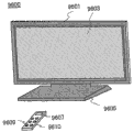
图27A是电视装置的示例的外视图并且图27B是数字相框的示例的外视图;27A is an external view of an example of a television set and FIG. 27B is an external view of an example of a digital photo frame;
图28A和28B每个图示游艺机的示例;以及28A and 28B each illustrate an example of an amusement machine; and
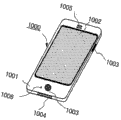
图29A和29B每个图示移动电话的示例。29A and 29B each illustrate an example of a mobile phone.
具体实施方式Detailed ways
实施例将参照附图描述。注意本发明不限于下文实施例中的说明,并且本发明的实施方式和细节可以采用各种方式改变而不偏离它的精神对于本领域内技术人员是明显的。此外,根据不同实施例的结构和方法可以用适当的组合实行。在下文描述的本发明的结构和方法中,相同的标号给予相同的部件或具有相似功能的部件,并且省略其重复说明。Embodiments will be described with reference to the drawings. Note that the present invention is not limited to the description in the following examples, and it will be obvious to those skilled in the art that the embodiments and details of the present invention can be changed in various ways without departing from its spirit. Furthermore, structures and methods according to different embodiments can be implemented in appropriate combinations. In structures and methods of the present invention described below, the same reference numerals are given to the same components or components having similar functions, and repeated explanations thereof are omitted.
在该说明书中,“膜”意思是在整个表面之上形成并且没有图案化的东西。“层,,意思是用抗蚀剂掩模或其类似物图案化成期望形状的东西。“膜,,和“层”之间的该区别是为了方便,并且在一些情况下使用它们而没有任何区别。同样关于堆叠层膜中的每层,在一些情况下使用“膜”和“层”而没有任何区别。In this specification, "film" means what is formed over the entire surface and is not patterned. "Layer" means something that is patterned into a desired shape with a resist mask or the like." This distinction between "film" and "layer" is for convenience, and in some cases they are used without any the difference. Also with respect to each layer in a stacked film, "film" and "layer" are used without any distinction in some cases.
注意在本说明书中,例如“第一”、“第二”和“第三”等包括在术语中的数字为方便而给出以便辨别元件,不限制数目、设置和步骤的顺序。Note that in this specification, numbers included in terms such as "first", "second" and "third" are given for convenience to identify elements and do not limit the number, arrangement and sequence of steps.
实施例1Example 1
在该实施例中,半导体器件和其的制造方法参照图1A和1B、图2A至2E、图3A至3C、图4A至4C、图5A1、5A2、5B1和5B2与图6描述。In this embodiment, a semiconductor device and its manufacturing method are described with reference to FIGS. 1A and 1B , FIGS. 2A to 2E , FIGS. 3A to 3C , FIGS. 4A to 4C , FIGS.
图1A和1B图示包括该实施例的薄膜晶体管的像素。图1A是平面图并且图1B是沿图1A中的线A1-A2获取的剖视图。1A and 1B illustrate a pixel including the thin film transistor of this embodiment. FIG. 1A is a plan view and FIG. 1B is a cross-sectional view taken along line A1 - A2 in FIG. 1A .
在图1A和1B中图示的薄膜晶体管150是所谓的反向交错薄膜晶体管。该薄膜晶体管150包括提供在衬底100之上的栅电极层101、覆盖该栅电极层101的栅极绝缘膜102、提供在该栅极绝缘膜102之上的氧化物半导体层107、提供在该氧化物半导体层107之上并且与其接触并且互相分开的一对氧化物半导体层111a和111b,以及分别与该对氧化物半导体层111a和111b接触并且互相分开的一对导电层110a和110b。The
氧化物半导体层107使用In-Ga-Zn-O基非单晶膜形成。另外,氧化物半导体层111a和111b(其使用具有比氧化物半导体层107更高电导率的In-Ga-Zn-O基非单晶膜形成)形成源区和漏区。此外,导电层110a和110b形成源电极层和漏电极层。起源电极和漏电极作用的导电层110a和110b(其互相分开形成)对应于互相分开形成的氧化物半导体层111a和111b。即,导电层110a提供在氧化物半导体层111a之上,并且导电层110b提供在氧化物半导体层111b之上。此外,每层图案化成期望的形状。注意氧化物半导体层111a和111b也称为n+层。The
在图1A和1B中图示的薄膜晶体管150是其中凹陷部分被包括在氧化物半导体层107中而它们置于形成源区和漏区的氧化物半导体层111a和111b之间的示例。这样的薄膜晶体管也称为沟道蚀刻型薄膜晶体管。The
在图1B中,阻挡膜113提供在导电层110a和110b之上。另外,该阻挡膜113提供为与氧化物半导体层107的一部分接触。该阻挡膜113提供成以便防止例如有机物质和金属;湿气;氧;以及在气氛中飘浮的类似物等杂质进入,并且优选地是致密膜。对例如湿气和氧等杂质的阻挡性质通过使用致密膜的形成提高。该阻挡膜113可以使用氧化铝膜、氮化铝膜、氧氮化铝膜或氮氧化铝膜形成为具有单层或堆叠层。该阻挡膜113的厚度优选地大于或等于1nm并且小于或等于200nm。注意该阻挡膜113的性质可以由X射线反射计(XRR)、热吸收能谱(TDS)、俄歇电子能谱(AES)或二次离子质谱(SIMS)发现。In FIG. 1B, a
当具有对湿气和氧的高阻挡性质的膜在氧化物半导体层之上形成以覆盖氧化物半导体层时,可以防止湿气和氧混合进入氧化物半导体层。因此,可以抑制氧化物半导体层的氧化还原反应和氧空位浓度中的变化。此外,可以防止例如有机物质和金属等包括在气氛中或在基底材料中的杂质混合进入氧化物半导体层。因此,可以抑制在其中使用氧化物半导体的半导体器件的半导体特性中的变化。此外,可以提高半导体器件的可靠性。When a film having a high barrier property to moisture and oxygen is formed over the oxide semiconductor layer to cover the oxide semiconductor layer, moisture and oxygen can be prevented from mixing into the oxide semiconductor layer. Therefore, oxidation-reduction reaction of the oxide semiconductor layer and variation in oxygen vacancy concentration can be suppressed. In addition, impurities such as organic substances and metals included in the atmosphere or in the base material can be prevented from being mixed into the oxide semiconductor layer. Therefore, variations in semiconductor characteristics of a semiconductor device in which an oxide semiconductor is used can be suppressed. In addition, the reliability of the semiconductor device can be improved.
在图1B中,在其中基底绝缘膜提供在衬底100和栅电极层101之间的情况下,该基底绝缘膜还可以使用氧化铝膜、氮化铝膜、氧氮化铝膜或氮氧化铝膜或其类似物形成为具有单层或堆叠层。当该基底绝缘膜使用致密膜形成时,可以防止湿气和氧从衬底100侧进入氧化物半导体层。另外,可以防止包括在衬底100中的杂质(例如碱金属(Li、Cs、Na或其类似物)、碱土金属(Ca、Mg或其类似物)或另一个金属元素等)进入氧化物半导体层。注意当半导体器件完成时,Na以小于或等于5×10¹⁹/cm3或优选地小于或等于1×1018/cm3包括在氧化物半导体层107中。从而,可以抑制其中使用氧化物半导体的半导体器件的半导体特性中的变化。因此,可以提高半导体器件的可靠性。In FIG. 1B, in the case where a base insulating film is provided between the
在图1A中图示的薄膜晶体管150可以应用于提供在由液晶显示器或电致发光(EL)显示器典型化的显示器的像素部分中的像素晶体管。因此,在图示的示例中,接触孔126提供在阻挡膜113中,像素电极层(透明导电层114)提供在阻挡膜113之上,并且该像素电极层(透明导电层114)和导电层110b通过提供在阻挡膜113中的该接触孔126互相连接。The
如在图1A中图示的,薄膜晶体管150的源电极和漏电极中的一个具有U形(或旋转的C形或马蹄形),并且环绕源电极和漏电极中的另一个。源电极和漏电极之间的距离保持几乎恒定。As illustrated in FIG. 1A , one of the source and drain electrodes of the
薄膜晶体管150具有上文的形状,由此薄膜晶体管150的沟道宽度可以增加并且从而电流量增加。此外,电特性中的变化可以减少。此外,可以抑制在制造工艺中由于掩模图案的未对准引起的可靠性的降低。该实施例不限于该形状,并且薄膜晶体管150的源电极和漏电极中的一个不是必须具有U形。The
接着,半导体器件的制造工艺的示例参照图2A至2E描述。Next, an example of a manufacturing process of a semiconductor device is described with reference to FIGS. 2A to 2E .
首先,栅电极层101在具有绝缘表面的衬底100之上形成,并且然后栅极绝缘膜102在栅电极层101之上形成。其后,氧化物半导体膜103和氧化物半导体膜104形成为堆叠的(参见图2A)。First, a
作为具有绝缘表面的衬底100,可以使用例如用于液晶显示器或其类似物的具有透可见光性质的玻璃衬底。前面提到的玻璃衬底优选地是无碱玻璃衬底。作为无碱玻璃衬底的材料,例如,使用例如铝硅玻璃、铝硼硅玻璃或硼硅酸钡玻璃等玻璃材料。另外,作为具有绝缘表面的衬底100,可以使用由例如陶瓷衬底、石英衬底或蓝宝石衬底等绝缘体形成的绝缘衬底;用例如硅等半导体材料形成并且其的表面用绝缘材料覆盖的半导体衬底;用例如金属或不锈钢等导体形成并且其的表面用绝缘材料覆盖的导电衬底;或其类似物。As the
注意如在图2A中图示的,将成为基底膜的绝缘膜130可提供在具有绝缘表面的衬底100之上。该绝缘膜130具有防止杂质从衬底100扩散的功能,例如碱金属(Li、Cs、Na或其类似物)、碱土金属(Ca、Mg或其类似物)或另一个金属元素等。注意当半导体器件完成时,Na以小于或等于5×10¹⁹/cm3或优选地小于或等于1×1018/cm3包括在氧化物半导体层107中。该绝缘膜130可以形成为具有从氮化硅膜、氧化硅膜、氮氧化硅膜、氧氮化硅膜、氧化铝膜、氮化铝膜、氧氮化铝膜和氮氧化铝膜选择的一个或多个膜的堆叠结构。Note that, as illustrated in FIG. 2A , an insulating
在导电膜在衬底100之上形成后,该导电膜使用通过光刻方法形成的抗蚀剂掩模选择性蚀刻,由此可以形成栅电极层101。在该情况下,为了改进与稍后形成的栅极绝缘膜102的覆盖并且防止断开,栅电极层101的边缘部分优选地被蚀刻以便具有锥形。注意栅电极层101包括电极和布线,其使用该导电膜形成,例如栅极布线等。After the conductive film is formed over the
栅电极层101可以使用例如铝、铜、钼、钛、铬、钽或钨等金属材料;包括这些材料中的任何材料作为主要成分的合金材料;包括这些材料中的任何材料作为主要成分的氮化物形成为具有单层或堆叠层。栅电极层101可取地使用例如铝等低电阻导电材料形成。注意在其中铝用于布线和电极的情况下,因为单独使用铝带来例如低耐热性和易于被腐蚀等劣势,铝优选地与耐热导电材料结合使用。For the
作为耐热导电材料,可以使用从钛、钽、钨、钼和铬选择的元素、或包括这些元素中的任何元素的合金、包括这些元素的组合的合金膜或包括这些元素中的任何元素的氮化物。用这样的耐热导电材料和铝(或铜)形成的膜被堆叠,使得可以形成布线和电极。As the heat-resistant conductive material, an element selected from titanium, tantalum, tungsten, molybdenum, and chromium, or an alloy including any of these elements, an alloy film including a combination of these elements, or an alloy including any of these elements can be used. nitride. Films formed of such a heat-resistant conductive material and aluminum (or copper) are stacked so that wiring and electrodes can be formed.
栅极绝缘膜102可以使用氧化硅膜、氧氮化硅膜、氮化硅膜、氮氧化硅膜、氧化铝膜、氮化铝膜、氧氮化铝膜、氮氧化铝膜或氧化钽膜形成为具有单层或堆叠层。栅极绝缘膜102可以通过溅射法或其类似方法形成到大于或等于50nm并且小于或等于250nm的厚度。例如,作为栅极绝缘膜102,具有100nm厚度的氧化硅膜可以通过溅射法形成。备选地,具有100nm厚度的氧化铝膜可以通过溅射法形成。For the
当绝缘膜130或栅极绝缘膜102使用致密膜形成时,可以防止湿气和氧从衬底100侧进入氧化物半导体层。另外,可以防止包括在衬底100中的杂质(例如碱金属(Li、Cs、Na或其类似物)、碱土金属(Ca、Mg或其类似物)或另一个金属元素等)进入氧化物半导体层。注意当半导体器件完成时,Na以小于或等于5×10¹⁹/cm3或优选地小于或等于1×1018/cm3包括在氧化物半导体层107中。从而,可以抑制其中使用氧化物半导体的半导体器件的半导体特性中的变化。因此,可以提高半导体器件的可靠性。When insulating
在氧化物半导体膜103在栅极绝缘膜102之上形成之前,栅极绝缘膜102的表面可经受等离子体处理。通过等离子体处理,可以去除附着到栅极绝缘膜102的表面的灰尘。Before the
等离子体处理可以采用例如氩(Ar)气等惰性气体引入真空腔并且偏压施加到处理对象(这里,在衬底100之上形成的栅极绝缘膜102)以便产生等离子体状态这样的方式执行。在其中Ar气引入腔的情况下,电子和Ar的阳离子在等离子体中存在并且Ar的阳离子在阴极方向上加速(朝衬底100侧)。该加速的Ar阳离子与在衬底100之上形成的栅极绝缘膜102的表面碰撞,由此栅极绝缘膜102的表面通过溅射被蚀刻从而被重整。在一些情况下,上文描述的这样的等离子体处理还称为“反向溅射”。在该实施例中,在等离子体处理中偏压施加于衬底100侧。备选地,等离子体处理可执行而不施加偏压,只要栅极绝缘膜102的表面可以被重整即可。The plasma processing can be performed in such a manner that an inert gas such as argon (Ar) gas is introduced into the vacuum chamber and a bias voltage is applied to the processing object (here, the
代替氩气,氦气可用作在等离子体处理中使用的气体。备选地,可采用添加氧、氢、氮或其类似物的氩气氛。进一步备选地,可采用添加Cl2、CF4或其类似物的氩气氛。Instead of argon, helium can be used as the gas used in plasma processing. Alternatively, an argon atmosphere added with oxygen, hydrogen, nitrogen or the like may be employed. Further alternatively, an argon atmosphere added with Cl 2 , CF 4 or the like may be employed.
氧化物半导体膜103可以使用In-Ga-Zn-O基非单晶膜形成。例如,氧化物半导体膜103使用包括In、Ga和Zn(In2O3:Ga2O3:ZnO=1:1:1)的氧化物半导体靶通过溅射法形成。对于溅射可采用下列条件,例如:衬底100和靶之间的距离是30mm至500mm;压强是0.1Pa至2.0Pa;DC电源是0.25kW至5.0kW(当使用具有直径8英寸的尺寸的靶时);并且气氛是氩气氛、氧气氛或氩和氧的混合气氛。The
优选地使用脉冲DC电源,因为灰尘可以被减少并且厚度可以均匀化。另外,执行上文的等离子体处理,并且然后氧化物半导体膜103被形成而没有暴露于气氛,使得可以防止灰尘和湿气附着到栅极绝缘膜102和氧化物半导体膜103之间的界面。氧化物半导体膜103的厚度可以是大约5nm至200nm。It is preferable to use a pulsed DC power supply because dust can be reduced and the thickness can be made uniform. In addition, the above plasma treatment is performed, and then the
作为上文的溅射法,可以采用其中高频电源用作溅射电源的RF溅射法、DC溅射法、其中直流偏置(direct current bias)采用脉冲施加的脉冲DC溅射法或类似方法。RF溅射法主要在形成绝缘膜的情况下使用,并且DC溅射法主要在形成金属膜的情况下使用。As the above sputtering method, an RF sputtering method in which a high-frequency power source is used as a sputtering power source, a DC sputtering method, a pulsed DC sputtering method in which a direct current bias is applied with a pulse, or the like can be used. method. The RF sputtering method is mainly used in the case of forming an insulating film, and the DC sputtering method is mainly used in the case of forming a metal film.
备选地,可使用其中多个靶用互相不同的材料形成的多靶溅射设备。在多靶溅射设备中,不同膜的堆叠可以在一个腔中形成,或一个膜可以在一个腔中同时使用多种材料通过溅射形成。备选地,可采用使用其中磁场产生系统提供在腔内的磁控溅射设备的方法(磁控溅射法)、其中使用通过使用微波产生的等离子体的ECR溅射法或类似方法。进一步备选地,可采用其中靶物质和溅射气体成分在膜形成时互相化学反应以形成其的化合物的反应溅射法、其中电压在膜形成时也施加到衬底的偏置溅射法或类似方法。Alternatively, a multi-target sputtering apparatus may be used in which a plurality of targets are formed of mutually different materials. In a multi-target sputtering device, a stack of different films can be formed in one chamber, or one film can be formed by sputtering using multiple materials simultaneously in one chamber. Alternatively, a method using a magnetron sputtering apparatus in which a magnetic field generating system is provided inside a chamber (magnetron sputtering method), an ECR sputtering method in which plasma generated by using microwaves is used, or the like may be employed. Further alternatively, a reactive sputtering method in which a target substance and sputtering gas components chemically react with each other at the time of film formation to form its compound, a bias sputtering method in which a voltage is also applied to the substrate at the time of film formation may be employed or similar methods.
接着,具有比氧化物半导体膜103更高电导率的氧化物半导体膜104在氧化物半导体膜103之上形成。氧化物半导体膜104可以使用In-Ga-Zn-O基非单晶膜形成。例如,氧化物半导体膜104可以使用包括In、Ga和Zn(In2O3:Ga2O3:ZnO=1:1:1)的氧化物半导体靶通过溅射法在氧化物半导体膜103之上形成。Next, an
另外,氧化物半导体膜104可以使用用于形成氧化物半导体膜103的靶(In2O3:Ga2O3:ZnO=1:1:1)形成。至于溅射条件,例如,温度可以是20℃至100℃,压强可以是0.1Pa至2.0Pa,功率是250W至3kW(在8英寸Φ的情况下)。另外,氩气以40sccm的流率引入。通过视情况控制靶的成分的比例或其他溅射形成条件,可以控制晶粒的存在或不存在、密度等。晶粒的直径可以是大约1nm至10nm。氧化物半导体膜104的厚度可是大约2nm至20nm。不用说,当晶粒包括在膜中时,晶粒的尺寸不超过膜的厚度。In addition, the
这里,氧化物半导体膜103的形成条件不同于氧化物半导体膜104的那些是优选的。例如,使在氧化物半导体膜103的形成条件中的氧气与氩气的流率比大于在氧化物半导体膜104的形成条件中的氧气与氩气的流率比。具体地,对于氧化物半导体膜104的形成条件,采用稀有气体(氩、氦或其类似物)气氛、或包括10%或更少的氧气和90%或更多的稀有气体的气氛。对于氧化物半导体膜103的形成条件,采用氧气氛或其中氧气与稀有气体的流率比是1或更多的气氛。氧化物半导体膜104可接连形成使得氧化物半导体膜103不暴露于气氛。注意氧化物半导体膜103和氧化物半导体膜104可使用不同材料形成。Here, formation conditions of the
接着,抗蚀剂掩模106在氧化物半导体膜104之上形成,并且氧化物半导体膜103和氧化物半导体膜104使用该抗蚀剂掩模106选择性蚀刻,使得形成岛形氧化物半导体层107和岛形氧化物半导体层108(参见图2B)。Next, a resist
这时湿法蚀刻或干法蚀刻可以被用作蚀刻法。这里,岛形氧化物半导体层107和岛形氧化物半导体层108通过使用醋酸、硝酸和磷酸的混合溶液通过湿法蚀刻去除氧化物半导体膜103和氧化物半导体膜104的不必要部分而形成。注意在上文的蚀刻后,去除抗蚀剂掩模106。另外,用于湿法蚀刻的蚀刻剂不限于上文的溶液,只要氧化物半导体膜103和氧化物半导体膜104可以使用该蚀刻剂蚀刻即可。当执行干法蚀刻时,优选使用包括氯的气体或添加氧的包括氯的气体。这是因为通过使用包括氯和氧的气体,可以容易获得氧化物半导体膜103(以及氧化物半导体膜104)相对于栅极绝缘膜102的蚀刻选择性,并且可以足够减小对栅极绝缘膜102的损伤。At this time wet etching or dry etching may be used as the etching method. Here, the island-shaped
在该实施例中,描述其中堆叠氧化物半导体层107和具有比氧化物半导体层107更高电导率的氧化物半导体层108的示例。备选地,氧化物半导体层107的单层可以单独形成。In this embodiment, an example is described in which the
接着,导电膜在岛形氧化物半导体层107之上形成。该导电膜可以使用由包括从铝、铜、钛、钽、钨、钼、镍、锰、铬、钕和钪选择的元素的金属;包括上文的元素中的任何元素的合金;包括上文的元素中的任何元素的氮化物;或其类似物形成的材料通过溅射法、真空蒸发法或类似方法形成。注意在其中热处理(例如,以大约200℃至600℃的热处理)在该导电膜形成后执行的情况下,该导电膜优选地具有给定的耐热性。Next, a conductive film is formed over the island-shaped
例如,导电膜可以形成为具有钛膜的单层结构。备选地,导电膜可形成为具有堆叠层结构。例如,导电膜可以形成为具有铝膜和钛膜的堆叠层结构。进一步备选地,可采用钛膜、包括钕的铝(A1-Nd)膜和钛膜的三层结构。进一步备选地,导电膜可形成为具有包括硅的铝膜的单层结构。For example, the conductive film can be formed as a single-layer structure with a titanium film. Alternatively, the conductive film may be formed to have a stacked layer structure. For example, the conductive film may be formed to have a stacked layer structure of an aluminum film and a titanium film. Further alternatively, a three-layer structure of a titanium film, an aluminum (Al-Nd) film including neodymium (Al-Nd), and a titanium film may be employed. Further alternatively, the conductive film may be formed to have a single-layer structure of an aluminum film including silicon.
接着,抗蚀剂掩模109a和109b在导电膜之上形成,并且然后导电膜被选择性蚀刻以形成导电层110a和110b。同时,岛形氧化物半导体层108被蚀刻以形成具有比氧化物半导体层107更高电导率的半导体区(氧化物半导体层111a和111b),并且去除氧化物半导体层107的一部分(靠近其的表面的一部分),使得凹陷部分112在氧化物半导体层107中形成(参见图2C)。Next, resist
通过去除氧化物半导体层107的一部分形成的凹陷部分112对应于在导电层110a和导电层110b之间并且也在具有比氧化物半导体层107更高电导率的半导体区(氧化物半导体层111a)和具有比氧化物半导体层107更高电导率的半导体区(氧化物半导体层111b)之间的区域。因此,导电层110a起晶体管的源电极和漏电极中的一个的作用,而导电层110b起晶体管的源电极和漏电极中的另一个的作用。注意在上文的蚀刻后,去除抗蚀剂掩模109a和109b。The recessed
这时湿法蚀刻或干法蚀刻可以被用作蚀刻方法。这里,干法蚀刻优选地使用包括氯的气体执行。干法蚀刻的使用与使用湿法蚀刻的情况相比实现布线结构或其类似物的小型化。另外,氧化物半导体层107的去除可以由于干法蚀刻的高可控性而通过干法蚀刻高可控性地执行。更优选地,氧添加到包括氯的气体。这是因为通过使用包括氯和氧的气体,可以容易获得氧化物半导体层107(以及氧化物半导体层108)相对于栅极绝缘膜102的蚀刻选择性,并且可以足够减小对栅极绝缘膜102的损伤。At this time wet etching or dry etching may be used as the etching method. Here, dry etching is preferably performed using a gas including chlorine. The use of dry etching enables miniaturization of the wiring structure or the like compared to the case of using wet etching. In addition, removal of the
其后,热处理优选地在200℃至600℃、典型地300℃至500℃执行。这里,热处理在350℃在氮气氛下执行一小时。通过该热处理,执行包括在氧化物半导体层107和氧化物半导体层111a和111b中的In-Ga-Zn-O基氧化物半导体的原子水平的重排。该热处理(还包括光亮退火或其类似的)是重要的,因为该热处理实现了氧化物半导体层107和氧化物半导体层111a和111b中打断载流子传送的畸变的释放。注意对于上文的热处理的时间没有特定限制,只要热处理在氧化物半导体层107的形成之后执行即可。Thereafter, heat treatment is preferably performed at 200°C to 600°C, typically 300°C to 500°C. Here, heat treatment was performed at 350° C. for one hour under a nitrogen atmosphere. Through this heat treatment, rearrangement at the atomic level of the In-Ga-Zn-O-based oxide semiconductor included in the
接着,氧化物半导体层107的表面优选地在阻挡膜113形成之前经受等离子体处理。作为氧化物半导体层107的表面的等离子体处理,可执行由氧自由基的氧自由基处理或反向溅射。Next, the surface of the
由氧自由基的氧自由基处理优选地在02、N20、包括氧的N2、包括氧的He、包括氧的Ar或其类似的气氛中执行。备选地,氧自由基处理可在Cl2或CF4添加到上文的气氛的气氛中执行。注意自由基处理优选地在没有施加偏压到衬底100侧的情况下执行。通过执行氧自由基处理,其中岛形氧化物半导体层107包括沟道形成区的薄膜晶体管可以是常关断薄膜晶体管,其当电压没有施加到栅电极时处于关断状态。此外,通过执行自由基处理,可以恢复由于蚀刻造成的对岛形氧化物半导体层107的损伤。The oxygen radical treatment by oxygen radicals is preferably performed in an atmosphere of 0 2 , N 2 0, N 2 including oxygen, He including oxygen, Ar including oxygen, or the like. Alternatively, the oxygen radical treatment can be performed in an atmosphere with Cl or CF added to the above atmosphere. Note that the radical treatment is preferably performed without applying a bias voltage to the
反向溅射可以采用例如氩(Ar)气等惰性气体引入真空腔并且偏压施加到处理对象(这里,衬底100)使得产生等离子体状态这样的方式执行。在该情况下,电子和Ar的阳离子在等离子体中存在并且Ar的阳离子在阴极方向上加速(朝衬底100侧)。该加速的Ar阳离子与在衬底100之上形成的氧化物半导体层107、栅极绝缘膜102和导电层110a和110b的表面碰撞,由此表面通过溅射被蚀刻从而被重整。注意氦气可代替氩气使用。备选地,可使用添加氧、氢、氮或其类似物的氩气氛。进一步备选地,可使用添加Cl2、CF4或其类似物的氩气氛。The reverse sputtering can be performed in such a manner that an inert gas such as argon (Ar) gas is introduced into the vacuum chamber and a bias voltage is applied to the processing object (here, the substrate 100 ) so that a plasma state is generated. In this case, electrons and cations of Ar exist in the plasma and the cations of Ar are accelerated in the cathode direction (toward the
当氧化物半导体层107的表面经受反向溅射时,由于氧化物半导体层107的表面暴露于气氛形成的氧化物和吸收的有机物质可以通过蚀刻去除。另外,氧化物半导体层107的表面可以活化并且因此可以加强与接着形成的阻挡膜113的化学键。反向溅射优选地采用RF溅射法形成。这是因为当接着形成的阻挡膜113通过RF溅射法形成时,阻挡膜113可以形成而不暴露于气氛。When the surface of the
接着,形成阻挡膜113以覆盖包括栅电极层101、氧化物半导体层107、氧化物半导体层111a和111b、导电层110a和110b等的薄膜晶体管150(参见图2D)。阻挡膜113优选地形成为与其中氧化物半导体层107暴露的区域接触。阻挡膜可以使用氧化铝膜、氮化铝膜、氧氮化铝膜或氮氧化铝膜形成为具有单层或堆叠层。Next,
氧化物半导体层107和氧化物半导体层111a和111b的半导体特性受氧化物半导体层中的氧空位浓度显著影响。湿气和氧进入氧化物半导体层107和氧化物半导体层111a和111b显著影响氧化物半导体层中的半导体特性。阻挡膜113优选地使用能够防止例如有机物质和金属、湿气、氧以及在气氛中飘浮的类似物等杂质进入的致密膜形成。当氧化硅膜或氮化硅膜用作阻挡膜113时,对湿气和氧的阻挡性质通过由于膜中分子链等引起的硅原子的空位的存在而被阻止。相比之下,氧化铝膜或其类似物由于它的高密度而具有优于氧化硅膜、氮化硅膜或其类似物的阻挡性质。因此,氧化铝膜或其类似物作为氧化物半导体层的阻挡膜的使用可以防止例如湿气和氧等杂质进入氧化物半导体层。The semiconductor characteristics of the
在形成起阻挡膜113的作用的氧化铝膜的情况下,氧化铝膜通过溅射法例如在氩气氛中使用氧化铝(Al2O3)靶来形成。为了获得极高的透光性质,氧化铝膜可包括杂质,特别是以大于原子百分比0%和小于原子百分比2.5%的氮。氮浓度可以视情况通过溅射条件(衬底温度、源气体和其流率、形成压强等)的调节而调节。备选地,氧化铝膜可在包括氧气的气氛中使用铝(Al)靶形成。特别地,氧化铝膜使用具有Φ8英寸的铝靶并且采用下列条件通过RF溅射法形成:1kW的形成功率;0.4Pa的形成压强;以10sccm的流率的氩气;以5sccm的流率的氧气;靶和衬底之间的160mm的距离;膜形成中20℃至25℃的衬底温度;以及1.5nm/min的膜形成速率。In the case of forming an aluminum oxide film functioning as the
在形成起阻挡膜113的作用的氮化铝膜的情况下,氮化铝膜通过溅射法例如在氩气和氮气的混合气氛中使用氮化铝(AlN)靶形成。特别地,氮化铝膜使用氮化铝(AlN)靶在以20sccm的流率的氩气和以20sccm的流率的氮气的混合气氛中形成。氮化铝膜可包括杂质,特别地以原子百分比0%或更多并且小于原子百分比10%的氧。氧浓度可以视情况通过溅射条件(衬底温度、源气体和其的流率、形成压强等)的调节而调节。备选地,氮化铝膜可在包括氮气的气氛中使用铝(Al)靶形成。In the case of forming an aluminum nitride film functioning as the
在形成起阻挡膜113的作用的氮氧化铝膜的情况下,氮氧化铝膜通过溅射法例如在氩气、氮气和氧气的混合气氛中使用氮化铝(AlN)靶形成。特别地,氮氧化铝膜使用氮化铝(AlN)靶在以20sccm的流率的氩气、以15sccm的流率的氮气和以5sccm的流率的氧气的混合气氛中形成。氮氧化铝膜可包括以若干原子百分比或更多或优选地原子百分比2.5%至47.5%的氮。氮浓度可以视情况通过溅射条件(衬底温度、源气体和其的流率、形成压强等)的调节而调节。备选地,氮氧化铝膜可在包括氮气和氧气的气氛中使用铝(Al)靶形成。In the case of forming an aluminum oxynitride film functioning as the
注意用于形成这些膜的方法不限于溅射法。备选地,可采用蒸发法或另一个已知技术。Note that the method for forming these films is not limited to the sputtering method. Alternatively, evaporation or another known technique may be used.
另外,形成的阻挡膜113可经受等离子体处理或用例如臭氧水等具有高氧化性的溶液的处理使得阻挡膜113中的氧缺陷被修复。等离子体处理可在氧、氮、一氧化二氮或该气体和另一个气体的混合气体的气氛中执行。通过等离子体处理,阻挡膜可以更致密。In addition, the formed
当具有对湿气和氧的高阻挡性质的膜在氧化物半导体层之上形成以覆盖氧化物半导体层时,可以防止湿气和氧混合进入氧化物半导体层。因此,可以抑制氧化物半导体层的氧化还原反应和氧空位浓度中的变化。此外,可以防止例如有机物质和金属等在气氛中飘浮的杂质混合进入氧化物半导体层。因此,可以抑制在其中使用氧化物半导体的半导体器件的半导体特性中的变化。此外,可以提高半导体器件的可靠性。When a film having a high barrier property to moisture and oxygen is formed over the oxide semiconductor layer to cover the oxide semiconductor layer, moisture and oxygen can be prevented from mixing into the oxide semiconductor layer. Therefore, oxidation-reduction reaction of the oxide semiconductor layer and variation in oxygen vacancy concentration can be suppressed. In addition, impurities such as organic substances and metals floating in the atmosphere can be prevented from being mixed into the oxide semiconductor layer. Therefore, variations in semiconductor characteristics of a semiconductor device in which an oxide semiconductor is used can be suppressed. In addition, the reliability of the semiconductor device can be improved.
注意在其中起基底膜作用的绝缘膜130或栅极绝缘膜102使用氧化铝膜、氮化铝膜、氧氮化铝膜或氮氧化铝膜形成的情况下,可以采用上文的制造方法。Note that in the case where insulating
接着,抗蚀剂掩模在阻挡膜113之上形成并且阻挡膜113选择性蚀刻以形成接触孔。其后,形成透明导电层114(参见图2E)。这时的蚀刻优选地是使用氯气的干法蚀刻。Next, a resist mask is formed over the
透明导电层114可以使用氧化铟(In2O3)、氧化铟和氧化锡的合金(In2O3-SnO2,缩写成ITO)、氧化铟和氧化锌的合金(In2O3-ZnO)或其类似物通过溅射法、真空蒸发法或类似方法形成。例如,形成透明导电膜,并且然后抗蚀剂掩模在该透明导电膜之上形成。然后,不必要的部分通过蚀刻去除,使得可以形成透明导电层114。The transparent
通过上文的工艺,可以形成薄膜晶体管150。采用该方式,形成薄膜晶体管150,其中具有对例如湿气和氧等杂质的高阻挡性质的膜用于防止例如湿气和氧等杂质混合进入氧化物半导体。因此,可以抑制其中使用氧化物半导体的半导体器件的半导体特性中的变化,并且此外,可以提高半导体器件的可靠性。Through the above processes, the
接着,作为半导体器件的示例的显示器的制造工艺参照图3A至3C和图4A至4C描述。注意在图3A至3C和图4A至4C中图示的制造工艺的许多部分是在图2A至2E中图示的那些所共有的。因此,省略相同部分的说明并且在下文详细做出不同部分的说明。Next, a manufacturing process of a display as an example of a semiconductor device is described with reference to FIGS. 3A to 3C and FIGS. 4A to 4C . Note that many parts of the manufacturing process illustrated in FIGS. 3A-3C and 4A-4C are common to those illustrated in FIGS. 2A-2E . Therefore, descriptions of the same parts are omitted and descriptions of different parts are made in detail below.
首先,布线和电极(包括栅电极层101的栅极布线、电容器布线120和第一端子121)在具有绝缘表面的衬底100之上形成(参见图3A)。该电容器布线120和该第一端子121可以使用与栅电极层101相同的材料形成。注意衬底100的材料和栅电极层101的材料和形成方法可以参照图2A。另外,将成为基底膜的绝缘膜130可提供在具有绝缘表面的衬底100之上。绝缘膜130的材料和形成方法可以参照图2A。First, wiring and electrodes (gate wiring including
接着,栅极绝缘膜102在栅电极层101之上形成,并且岛形氧化物半导体层107和岛形氧化物半导体层108在栅电极层101之上形成且绝缘膜102插入其之间(参见图3B)。栅极绝缘膜102的材料和形成方法可以参照图2A。氧化物半导体层107和氧化物半导体层108的材料和形成方法可以参照图2A和2B。Next, the
接着,接触孔122在栅极绝缘膜102中形成使得第一端子121暴露,并且然后导电膜123形成以覆盖栅极绝缘膜102、氧化物半导体层107和氧化物半导体层108(参见图3C)Next, a
导电膜123可以使用由包括从铝(Al)、铜(Cu)、钛(Ti)、钽(Ta)、钨(W)、钼(M0)、铬(Cr)、钕(Nd)和钪(Sc)选择的元素的金属;包括上文的元素中的任何元素的合金;包括上文的元素中的任何元素的氮化物;或其类似物形成的材料通过溅射法、真空蒸发法或类似方法形成。注意在其中热处理(例如,以大约200℃至600℃的热处理)在导电膜123形成后执行的情况下,导电膜123优选地具有给定的耐热性。The
例如,导电膜123可以形成为具有钛膜的单层结构。备选地,导电膜123可形成为具有堆叠层结构。例如,导电膜123可以形成为具有铝膜和钛膜的堆叠层结构。进一步备选地,可采用钛膜、包括钕的铝(Al-Nd)膜和钛膜的三层结构。进一步备选地,导电膜123可形成为具有包括硅的铝膜的单层结构。导电膜123和第一端子121通过接触孔122互相电连接。For example, the
接着,抗蚀剂掩模109a、109b、109c和109d在导电膜123之上形成,并且然后导电膜123选择性蚀刻以形成导电层110a和110b、第二端子124和连接电极125。同时,氧化物半导体层108被蚀刻以形成具有比氧化物半导体层107更高的电导率的半导体区(氧化物半导体层111a和111b),并且去除(沟道蚀刻)氧化物半导体层107的一部分(靠近其的表面的一部分)使得凹陷部分112在氧化物半导体层107中形成(参见图4A)。Next, resist
氧化物半导体层111a和111b起晶体管的源区和漏区的作用。导电层110a起晶体管的源电极和漏电极中的一个的作用,并且导电层110b起晶体管的源电极和漏电极中的另一个的作用。第二端子124可以电连接到源极布线(包括导电层110a或导电层110b的源极布线)。另外,连接电极125可以通过在栅极绝缘膜102中形成的接触孔122直接连接到第一端子121。The
这里,作为该步骤中的蚀刻,优选执行干法蚀刻。干法蚀刻的使用与使用湿法蚀刻的情况相比实现布线结构或其类似物的小型化。另外,岛形氧化物半导体层107的去除可以由于干法蚀刻的高可控性通过干法蚀刻高可控性地执行。用于干法蚀刻的气体等可以参照图2C。注意在上文的蚀刻后,去除抗蚀剂掩模109a、109b、109c和109d。Here, as etching in this step, dry etching is preferably performed. The use of dry etching enables miniaturization of the wiring structure or the like compared to the case of using wet etching. In addition, removal of the island-shaped
接着,热处理优选地在200℃至600℃、典型地300℃至500℃执行。例如,热处理在350℃在氮气氛下执行一小时。通过该热处理,执行包括在氧化物半导体层107和氧化物半导体层111a和111b中的In-Ga-Zn-O基非单晶膜的原子水平的重排。因为打断载流子传送的畸变可以通过该热处理释放,这里的热处理(还包括光亮退火或其类似的)是有效的。注意对于热处理的时间没有特定限制,只要热处理在氧化物半导体层107和氧化物半导体层111a和111b的形成之后执行即可。例如,热处理可在像素电极形成之后执行。Next, heat treatment is preferably performed at 200°C to 600°C, typically 300°C to 500°C. For example, heat treatment is performed at 350° C. for one hour under a nitrogen atmosphere. Through this heat treatment, rearrangement at the atomic level of the In-Ga-Zn-O-based non-single-crystal film included in the
接着,氧化物半导体层107的表面优选地在阻挡膜113形成之前经受等离子体处理。作为氧化物半导体层107的表面的等离子体处理,可执行由氧自由基的氧自由基处理或反向溅射。Next, the surface of the
由氧自由基的氧自由基处理优选地在O2、N2O、包括氧的N2、包括氧的He、包括氧的Ar或其类似的气氛中执行。备选地,氧自由基处理可在其中Cl2或CF4添加到上文的气氛的气氛中执行。注意自由基处理优选地在没有施加偏压到衬底100侧的情况下执行。通过执行氧自由基处理,其中岛形氧化物半导体层107包括沟道形成区的薄膜晶体管可以是常关断晶体管,其当电压没有施加到栅电极时处于关断状态。此外,通过执行自由基处理,可以恢复由于蚀刻造成的对岛形氧化物半导体层107的损伤。The oxygen radical treatment by oxygen radicals is preferably performed in an atmosphere of O 2 , N 2 O, N 2 including oxygen, He including oxygen, Ar including oxygen, or the like. Alternatively, the oxygen radical treatment can be performed in an atmosphere where Cl2 or CF4 is added to the above atmosphere. Note that the radical treatment is preferably performed without applying a bias voltage to the
反向溅射可以采用例如氩(Ar)气等惰性气体引入真空腔并且偏压施加到处理对象(这里,衬底100)使得产生等离子体状态这样的方式执行。在该情况下,电子和Ar的阳离子在等离子体中存在并且Ar的阳离子在阴极方向上加速(朝衬底100侧)。该加速的Ar阳离子与在衬底100之上形成的氧化物半导体层107、栅极绝缘膜102和导电层110a和110b的表面碰撞,由此表面通过溅射被蚀刻从而被重整。注意氦气可代替氩气使用。备选地,可使用添加氧、氢、氮或其类似物的氩气氛。进一步备选地,可使用添加Cl2、CF4或其类似物的氩气氛。The reverse sputtering can be performed in such a manner that an inert gas such as argon (Ar) gas is introduced into the vacuum chamber and a bias voltage is applied to the processing object (here, the substrate 100 ) so that a plasma state is generated. In this case, electrons and cations of Ar exist in the plasma and the cations of Ar are accelerated in the cathode direction (toward the
当氧化物半导体层107的表面经受反向溅射时,由于氧化物半导体层107的表面暴露于气氛形成的氧化物和吸收的有机物质可以通过蚀刻去除。另外,氧化物半导体层107的表面可以活化并且因此可以加强与接着形成的阻挡膜113的化学键。反向溅射优选地采用RF溅射法形成。这是因为当接着形成的阻挡膜113通过RF溅射法形成时,阻挡膜113可以形成而不暴露于气氛。When the surface of the
接着,阻挡膜113在薄膜晶体管150之上形成。阻挡膜113优选地提供为与其中氧化物半导体层107暴露的区域接触。阻挡膜113优选地使用致密膜形成,因为阻挡膜113被形成以防止例如有机物质或金属、湿气、氧或在气氛中飘浮的类似物等杂质进入。对例如湿气和氧等杂质的阻挡性质通过使用致密膜形成而提高。阻挡膜113可以通过溅射法或类似方法使用氧化铝膜、氮化铝膜、氧氮化铝膜或氮氧化铝膜形成为具有单层或堆叠层。阻挡膜113的制造方法可以参照图2D。Next, a
另外,形成的阻挡膜113可经受等离子体处理或用例如臭氧水等具有高氧化性的溶液的处理使得阻挡膜中的氧缺陷被修复。等离子体处理可在氧、氮、一氧化二氮或该气体和另一个气体的混合气体的气氛中执行。通过等离子体处理,阻挡膜可以更致密。In addition, the formed
当具有对湿气和氧的高阻挡性质的膜在氧化物半导体层之上形成以覆盖氧化物半导体层时,可以防止湿气和氧混合进入氧化物半导体层。因此,可以抑制氧化物半导体层的氧化还原反应和氧空位浓度中的变化。此外,可以防止例如有机物质和金属等在气氛中飘浮的杂质混合进入氧化物半导体层。因此,可以抑制其中使用氧化物半导体的半导体器件的半导体特性中的变化。因此,可以提高半导体器件的可靠性。When a film having a high barrier property to moisture and oxygen is formed over the oxide semiconductor layer to cover the oxide semiconductor layer, moisture and oxygen can be prevented from mixing into the oxide semiconductor layer. Therefore, oxidation-reduction reaction of the oxide semiconductor layer and variation in oxygen vacancy concentration can be suppressed. In addition, impurities such as organic substances and metals floating in the atmosphere can be prevented from being mixed into the oxide semiconductor layer. Therefore, variations in semiconductor characteristics of a semiconductor device in which an oxide semiconductor is used can be suppressed. Therefore, the reliability of the semiconductor device can be improved.
然后,抗蚀剂掩模在阻挡膜113之上形成,并且阻挡膜113选择性蚀刻使得形成达到导电层110b的接触孔126b、达到连接电极125的接触孔126c以及达到第二端子124的接触孔126a(参见图4B)。在该步骤中的蚀刻优选地通过采用使用氯气的干法蚀刻执行。Then, a resist mask is formed over the
接着,形成电连接到导电层110b的透明导电层114a、电连接到连接电极125的透明导电层114c以及电连接到第二端子124的透明导电层114b(参见图4C)。在该步骤的顶视图对应于图1A。Next, a transparent
透明导电层114a、114b和114c可以使用氧化铟(In2O3)、氧化铟和氧化锡的合金(In2O3-SnO2,在下文中缩写成ITO)、氧化铟和氧化锌的合金(In2O3-ZnO)或其类似物通过溅射法、真空蒸发法或类似方法形成。例如,形成透明导电膜,并且然后抗蚀剂掩模在该透明导电膜之上形成。然后,不必要的部分通过蚀刻去除,使得可以形成透明导电层114a、114b和114c。The transparent
透明导电层114a起像素电极的作用。透明导电层114b和114c充当用于连接到FPC的电极或布线。特别地,在连接电极125之上形成的透明导电层114c可以用作起栅极布线的输入端子的作用的连接端子电极。在第二端子124之上形成的透明导电层114b可以用作起源极布线的输入端子的作用的连接端子电极。The transparent
另外,电容器布线120、栅极绝缘膜102、阻挡膜113和透明导电层114a可以形成存储电容器。在该情况下,电容器布线120和透明导电层114a充当电极,并且栅极绝缘膜102和阻挡膜113充当电介质。In addition, the
此外,图5A1和5A2分别是该步骤的栅极布线端子部分的剖视图和其的顶视图。图5A1是沿图5A2的线C1-C2获取的剖视图。在图5A1中,在阻挡膜113之上形成的透明导电层114c是起输入端子作用的连接端子电极。此外,在图5A1中,在端子部分中,使用与栅极布线相同的材料形成的第一端子121和使用与源极布线相同的材料形成的连接电极125互相重叠且栅极绝缘膜102插入其之间,并且在端子部分互相直接接触以处于导通。另外,连接电极125和透明导电层114c通过在阻挡膜113中形成的接触孔互相直接接触并且处于导通。In addition, FIGS. 5A1 and 5A2 are a sectional view of the gate wiring terminal portion of this step and a top view thereof, respectively. FIG. 5A1 is a cross-sectional view taken along line C1 - C2 of FIG. 5A2 . In FIG. 5A1, a transparent
图5B1和5B2分别是源极布线端子部分的剖视图和顶视图。图5B1对应于沿图5B2中的线D1-D2获取的剖视图。在图5B1中,在阻挡膜113之上形成的透明导电层114b是起输入端子作用的连接端子电极。另外,图5B1图示其中材料与栅极布线的材料相同的电极127放置在电连接到源极布线的第二端子124下面并且在端子部分与第二端子124重叠且栅极绝缘层152插入其之间的情况。电极127不电连接到第二端子124。如果电极127设置到不同于第二端子124的电势的电势,例如浮动、GND或0V等,可以形成抵御噪声或静电有用的电容器。另外,第二端子124电连接到透明导电层114b且阻挡膜113插入其之间。5B1 and 5B2 are a sectional view and a top view of a source wiring terminal portion, respectively. FIG. 5B1 corresponds to a cross-sectional view taken along line D1 - D2 in FIG. 5B2 . In FIG. 5B1, a transparent
根据像素密度提供多个栅极布线、源极布线和电容器布线。同样在端子部分中,设置处于与栅极布线相同的电势的多个第一端子、处于与源极布线相同的电势的多个第二端子、处于与电容器布线相同的电势的多个第三端子等。对于端子中的每个的数目没有特定限制,并且端子的数目可由从业者视情况确定。A plurality of gate wirings, source wirings, and capacitor wirings are provided according to pixel density. Also in the terminal portion, a plurality of first terminals at the same potential as the gate wiring, a plurality of second terminals at the same potential as the source wiring, a plurality of third terminals at the same potential as the capacitor wiring are provided wait. There is no specific limit to the number of each of the terminals, and the number of terminals can be determined by a practitioner as appropriate.
通过上文的工艺,例如n沟道底栅极薄膜晶体管和存储电容器等元件可以使用六个光掩模完成。另外,这些元件采用矩阵设置以便对应于相应像素,由此可以获得用于制造有源矩阵显示器的一个衬底。在该说明书中,这样的衬底为了方便称为有源矩阵衬底。Through the above processes, elements such as n-channel bottom-gate thin film transistors and storage capacitors can be completed using six photomasks. In addition, these elements are arranged in a matrix so as to correspond to corresponding pixels, whereby one substrate for manufacturing an active matrix display can be obtained. In this specification, such a substrate is referred to as an active matrix substrate for convenience.
当制造有源矩阵液晶显示器时,有源矩阵衬底和提供有对电极的对衬底互相接合且液晶层插入其之间。注意电连接到对衬底上的对电极的公共电极提供在有源矩阵衬底之上,并且电连接到该公共电极的第四端子提供在端子部分中。提供该第四端子使得该公共电极固定到例如GND或0V等预定电势。When manufacturing an active matrix liquid crystal display, an active matrix substrate and a counter substrate provided with a counter electrode are bonded to each other with a liquid crystal layer interposed therebetween. Note that a common electrode electrically connected to the counter electrode on the counter substrate is provided over the active matrix substrate, and a fourth terminal electrically connected to the common electrode is provided in the terminal portion. The fourth terminal is provided so that the common electrode is fixed to a predetermined potential such as GND or 0V.
根据该实施例的结构不限于在图1A中图示的像素结构。结构的另一个示例在图6中图示。图6图示其中像素电极和邻近像素的栅极布线充当电极,并且阻挡膜和栅极绝缘膜充当电介质,由此存储电容器被形成而没有电容器布线的结构。在该情况下,可以省略电容器布线和连接到电容器布线的第三端子。The structure according to this embodiment is not limited to the pixel structure illustrated in FIG. 1A. Another example of a structure is illustrated in FIG. 6 . 6 illustrates a structure in which a pixel electrode and a gate wiring of an adjacent pixel serve as an electrode, and a barrier film and a gate insulating film serve as a dielectric, whereby a storage capacitor is formed without a capacitor wiring. In this case, the capacitor wiring and the third terminal connected to the capacitor wiring can be omitted.
该实施例可以视情况与其他实施例中的任何实施例结合实现。This embodiment can be implemented in combination with any of the other embodiments as appropriate.
实施例2Example 2
在该实施例中,不同于实施例1的半导体器件的半导体器件及其制造工艺参照图7A和7B、图8A至8C、图9A和9B以及图10A至10C描述。注意在该实施例中描述的半导体器件和制造工艺的许多部分与在实施例1中描述的那些相同。因此,省略相同部分的说明并且在下文详细做出不同部分的说明。In this embodiment, a semiconductor device different from that of
图7A和7B图示该实施例的薄膜晶体管。图7A是平面图,并且图7B是沿图7A中的线A1-A2获取的剖视图。7A and 7B illustrate the thin film transistor of this embodiment. FIG. 7A is a plan view, and FIG. 7B is a cross-sectional view taken along line A1 - A2 in FIG. 7A .
图7A和7B图示其中栅电极层201在具有绝缘表面的衬底200之上形成并且栅极绝缘膜202在该栅电极层201之上形成的薄膜晶体管250。起源电极和漏电极作用的导电层210a和210b提供在该栅极绝缘膜202之上与该栅电极层201重叠。另外,氧化物半导体层211a和211b分别提供在该导电层210a和210b之上。氧化物半导体层207提供为覆盖氧化物半导体层211a和211b。该氧化物半导体层207使用In-Ga-Zn-O基非单晶膜形成。该氧化物半导体层211a和211b(其是具有比该氧化物半导体层207更高电导率的In-Ga-Zn-O基非单晶膜)形成源区和漏区。注意该氧化物半导体层211a和211b也称为n+层。7A and 7B illustrate a
另外,如在图7B中图示的,阻挡膜213提供为与氧化物半导体层207接触,并且透明导电层214提供为以便在阻挡膜213的接触孔中接触导电层210b。In addition, as illustrated in FIG. 7B , a
在图7A和7B中图示的薄膜晶体管250具有叫做底栅极底接触结构的结构。在该实施例中描述的半导体器件中,栅极绝缘膜202在包括薄膜晶体管250的所有区域中存在,并且栅电极层201提供在栅极绝缘膜202和具有绝缘表面的衬底200之间。另外,包括起源电极和漏电极作用的导电层210a和210b的布线提供在栅极绝缘膜202之上,并且氧化物半导体层207提供在导电层210a和210b之上。此外,该布线延伸到氧化物半导体层207的外围部分的外面。氧化物半导体层211a和211b分别堆叠在导电层210a和210b之上。The
接着,半导体器件的制作工艺的示例参照图8A至8C以及图9A和9B描述。Next, an example of a manufacturing process of a semiconductor device is described with reference to FIGS. 8A to 8C and FIGS. 9A and 9B .
首先,栅电极层201在具有绝缘表面的衬底200之上形成。继续,栅极绝缘膜202在栅电极层201之上形成(参见图8A)。First, a
衬底200的材料、栅电极层201和栅极绝缘膜202的材料和形成方法可以参照在实施例1中描述的衬底100、栅电极层101和栅极绝缘膜102。另外,起基底绝缘膜的作用的绝缘膜230可提供在具有绝缘表面的衬底200之上。绝缘膜230的材料和形成方法可以参照在实施例1中描述的绝缘膜130。The material of the
然后,导电膜在栅极绝缘膜202之上形成。该导电膜的材料和形成方法可以参照在实施例1中描述的导电膜123。Then, a conductive film is formed over the
继续,第一氧化物半导体膜在导电膜之上形成。该第一氧化物半导体膜的材料和形成方法可以参照在实施例1中描述的氧化物半导体膜104。注意导电膜和该第一氧化物半导体膜优选地接连形成。导电膜和该第一氧化物半导体膜通过溅射法形成而不暴露于空气,使得在制造工艺中可以防止由于导电膜的暴露而造成灰尘粘附到导电膜。Continuing, a first oxide semiconductor film is formed over the conductive film. The material and formation method of the first oxide semiconductor film can refer to the
接着,抗蚀剂掩模在第一氧化物半导体膜之上形成。导电膜和第一氧化物半导体膜的不必要部分使用该抗蚀剂掩模通过选择性蚀刻去除以形成导电层210a和210b以及氧化物半导体层211a和211b(参见图8B)。氧化物半导体层211a和211b起源区和漏区的作用。导电膜和第一氧化物半导体膜可以通过湿法蚀刻或干法蚀刻来蚀刻。Next, a resist mask is formed over the first oxide semiconductor film. Unnecessary portions of the conductive film and the first oxide semiconductor film are removed by selective etching using this resist mask to form
接着,具有比第一氧化物半导体膜更低电导率的第二氧化物半导体膜在氧化物半导体层211a和211b之上形成。该第二氧化物半导体膜的材料和形成方法可以参照在实施例1中描述的氧化物半导体膜103。Next, a second oxide semiconductor film having a lower conductivity than the first oxide semiconductor film is formed over the
接着,抗蚀剂掩模在第二氧化物半导体膜之上形成。第二氧化物半导体膜的不必要部分使用该抗蚀剂掩模通过选择性蚀刻去除,使得形成氧化物半导体层207(参见图8C)。此外,这时,也蚀刻除了与氧化物半导体层207重叠的区域的氧化物半导体层211a和211b的部分。第二氧化物半导体膜可以通过湿法蚀刻或干法蚀刻来蚀刻。Next, a resist mask is formed over the second oxide semiconductor film. Unnecessary portions of the second oxide semiconductor film are removed by selective etching using this resist mask, so that an
在该实施例中,描述其中提供氧化物半导体层211a和211b与具有比氧化物半导体层211a和211b更低电导率的氧化物半导体层207的示例。备选地,单层氧化物半导体层207可以单独形成。In this embodiment, an example is described in which the oxide semiconductor layers 211 a and 211 b and the
其后,热处理优选地在200℃至600℃、典型地300℃至500℃执行。这里,热处理在350℃在氮气氛下执行一小时。通过该热处理,执行包括在岛形氧化物半导体层207和氧化物半导体层211a和211b中的In-Ga-Zn-O基氧化物半导体的原子水平的重排。该热处理(还包括光亮退火或其类似的)是重要的,因为该热处理实现岛形氧化物半导体层207中打断载流子传送的畸变的释放。注意对于上文的热处理的时间没有特定限制,只要热处理在氧化物半导体层207和氧化物半导体层211a和211b的形成之后执行即可。Thereafter, heat treatment is preferably performed at 200°C to 600°C, typically 300°C to 500°C. Here, heat treatment was performed at 350° C. for one hour under a nitrogen atmosphere. Through this heat treatment, rearrangement at the atomic level of the In-Ga-Zn-O-based oxide semiconductor included in the island-shaped
氧化物半导体层207的表面优选地在阻挡膜213形成之前经受等离子体处理。作为氧化物半导体层207的表面的等离子体处理,可执行由氧自由基的氧自由基处理或反向溅射。在氧化物半导体层207的表面上执行的氧自由基处理或反向溅射的方法可以参照在实施例1中描述的在氧化物半导体层107的表面上执行的氧自由基处理或反向溅射的方法。The surface of the
接着,阻挡膜213在薄膜晶体管250之上形成(参见图9A)。阻挡膜213优选地提供为与氧化物半导体层207接触。阻挡膜213优选地使用致密膜形成,因为阻挡膜213形成为以便防止例如有机物质和金属、湿气、氧或在气氛中飘浮的类似物等杂质进入。对例如湿气和氧等杂质的阻挡性质通过用致密膜形成提高。阻挡膜213可以通过溅射法或类似方法使用氧化铝膜、氮化铝膜、氧氮化铝膜或氮氧化铝膜形成为具有单层或堆叠层。阻挡膜213的制造方法可以参照在实施例1中描述的阻挡膜113。另外,形成的阻挡膜213可经受等离子体处理或用例如臭氧水等具有高氧化性的溶液的处理使得阻挡膜中的氧缺陷被修复。Next, a
当具有对湿气和氧的高阻挡性质的膜在氧化物半导体层之上形成以覆盖氧化物半导体层时,可以防止湿气和氧混合进入氧化物半导体层。因此,可以抑制氧化物半导体层的氧化还原反应和氧空位浓度中的变化。此外,可以防止例如有机物质或金属等在气氛中飘浮的杂质混合进入氧化物半导体层。因此,可以抑制其中使用氧化物半导体的半导体器件的半导体特性中的变化,并且此外,可以提高半导体器件的可靠性。When a film having a high barrier property to moisture and oxygen is formed over the oxide semiconductor layer to cover the oxide semiconductor layer, moisture and oxygen can be prevented from mixing into the oxide semiconductor layer. Therefore, oxidation-reduction reaction of the oxide semiconductor layer and variation in oxygen vacancy concentration can be suppressed. In addition, impurities such as organic substances or metals floating in the atmosphere can be prevented from being mixed into the oxide semiconductor layer. Therefore, variation in semiconductor characteristics of a semiconductor device in which an oxide semiconductor is used can be suppressed, and furthermore, reliability of the semiconductor device can be improved.
接着,抗蚀剂掩模在阻挡膜213之上形成,并且阻挡膜213选择性蚀刻以形成达到导电层210b的接触孔。其后,形成透明导电层214(参见图9B)。这时的蚀刻优选地使用氯气干法蚀刻。注意在该步骤的顶视图对应于图7A。该透明导电层214的材料和形成方法可以参照在实施例1中描述的透明导电层114。Next, a resist mask is formed over the
通过上文的工艺,可以形成薄膜晶体管250。采用该方式,形成薄膜晶体管250,其中具有对例如湿气和氧等杂质的高阻挡性质的膜用于防止例如湿气和氧等杂质混合进入氧化物半导体。因此,可以抑制其中使用氧化物半导体的半导体器件的半导体特性中的变化,并且此外,可以提高半导体器件的可靠性。Through the above processes, the
在该实施例中描述的半导体器件和其的制造工艺不限于在图7A和7B、图8A至8C以及图9A和9B中图示的那些。该实施例的另一个半导体器件和其的另一个制造工艺参照图10A至10C描述。注意省略与图7A和7B、图8A至8C以及图9A和9B相同的部分的说明并且做出不同部分的说明。The semiconductor device and its manufacturing process described in this embodiment are not limited to those illustrated in FIGS. 7A and 7B , FIGS. 8A to 8C , and FIGS. 9A and 9B . Another semiconductor device of this embodiment and another manufacturing process thereof are described with reference to FIGS. 10A to 10C. Note that descriptions of the same parts as in FIGS. 7A and 7B , FIGS. 8A to 8C , and FIGS. 9A and 9B are omitted and descriptions of different parts are made.
在图10A中,绝缘膜230、栅电极层201、栅极绝缘膜202、导电层210a和210b以及氧化物半导体层211a和211b根据在图8A和8B中图示的方法在衬底200之上形成。In FIG. 10A, an insulating
接着,具有比氧化物半导体层211a和211b更低电导率的氧化物半导体膜203在氧化物半导体层211a和211b之上形成。氧化物半导体膜203的材料和形成方法可以参照在实施例1中描述的氧化物半导体膜103。Next, an
接着,阻挡膜213在氧化物半导体膜203之上形成(参见图10B)。阻挡膜213的材料和形成方法可以参照在实施例1中描述的阻挡膜113。Next, a
接着,层间绝缘膜231在阻挡膜213之上形成。该层间绝缘膜231可以使用由例如丙烯酸树脂,聚酰亚胺树脂,聚酰胺树脂,酚醛树脂,酚醛清漆树脂,三聚氰胺甲醛树脂,环氧树脂,聚氨酯树脂或其类似物等有机材料形成的绝缘膜形成。此外,对于该层间绝缘膜231,可以使用由例如氧化硅膜、氮化硅膜、氧氮化硅膜或氮氧化硅膜等无机材料、或硅氧烷(包括用硅(Si)和氧(O)的键形成的骨架结构)树脂形成的绝缘膜,或也可使用由有机材料形成的这些绝缘膜中的任何绝缘膜和用无机材料形成的这些绝缘膜中的任何绝缘膜的堆叠层。Next, an
接着,抗蚀剂掩模在层间绝缘膜231之上形成,并且层间绝缘膜231、阻挡膜213、氧化物半导体膜203和氧化物半导体层211b被选择性蚀刻,使得形成达到导电层210b的接触孔。其后,形成透明导电层214(参见图10C)。Next, a resist mask is formed over the
在图10中图示的半导体器件可以形成而没有蚀刻氧化物半导体膜203。因此,可以省略用于蚀刻氧化物半导体膜203的掩模,使得制造工艺与在图7A和7B、图8A至8C以及图9A和9B中图示的相比可以简化。The semiconductor device illustrated in FIG. 10 can be formed without etching the
该实施例可以视情况与其他实施例中的任何实施例结合实现。This embodiment can be implemented in combination with any of the other embodiments as appropriate.
实施例3Example 3
在该实施例中,不同于实施例1和2的那些半导体器件的半导体器件和其的制造工艺参照图11A和11B以及图12A至12D描述。注意在该实施例中描述的制造工艺的许多部分与在实施例1和2中描述的那些相同。因此,省略相同部分的说明并且在下文详细做出不同部分的说明。In this embodiment, a semiconductor device different from those of
图11A和11B图示该实施例的薄膜晶体管。图11A是平面图,并且图11B是沿图11A中的线A1-A2获取的剖视图。11A and 11B illustrate the thin film transistor of this embodiment. FIG. 11A is a plan view, and FIG. 11B is a cross-sectional view taken along line A1 - A2 in FIG. 11A .
图11A和11B图示其中栅电极层301在具有绝缘表面的衬底300之上形成并且栅极绝缘膜302在该栅电极层301之上形成的薄膜晶体管350。氧化物半导体层307和覆盖与该氧化物半导体层307的沟道形成区重叠的区域的沟道保护层315在该栅极绝缘膜302之上形成。导电层310a和310b形成为以便在该栅电极层301之上互相面对,其中该氧化物半导体层307插入其之间。11A and 11B illustrate a
氧化物半导体层307提供在互相面对的导电层310a和310b下面以覆盖栅电极层301,其中栅极绝缘膜302插入氧化物半导体层307和栅电极层301之间。即,氧化物半导体层307提供为与覆盖与沟道形成区重叠的区域的沟道保护层315的底面、与栅电极层301重叠的栅极绝缘膜302的顶面以及氧化物半导体层311a和311b的底面接触。这里,第二氧化物半导体层311a和导电层310a采用该顺序从氧化物半导体层307侧堆叠。采用相似的方式,氧化物半导体层311b和导电层310b采用该顺序从氧化物半导体层307侧堆叠。氧化物半导体层307使用In-Ga-Zn-O基非单晶膜形成。氧化物半导体层311a和311b(其是具有比氧化物半导体层307更高电导率的In-Ga-Zn-O基非单晶层)形成源区和漏区。注意该氧化物半导体层311a和311b也称为n+层。阻挡膜313和透明导电层314如在图11A和11B中示出的那样提供。The
图11B图示反向交错(底栅极)晶体管的横截面结构。特别地,在图11B中图示的晶体管具有沟道保护(沟道终止)结构。Figure 1 IB illustrates the cross-sectional structure of an inverted staggered (bottom gate) transistor. In particular, the transistor illustrated in FIG. 11B has a channel protection (channel termination) structure.
接着,半导体器件的制造工艺的示例参照图12A至12D描述。Next, an example of a manufacturing process of a semiconductor device is described with reference to FIGS. 12A to 12D .
首先,栅电极层301在具有绝缘表面的衬底300之上形成。继续,栅极绝缘膜302在栅电极层301之上形成。衬底300的材料、栅电极层301和栅极绝缘膜302的材料和形成方法可以参照在实施例1中描述的衬底100、栅电极层101和栅极绝缘膜102。另外,可提供起基底绝缘膜的作用的绝缘膜330。First, a
接着,第一氧化物半导体膜303在电极层301之上形成,其中栅极绝缘膜302插入其之间(参见图12A)。该第一氧化物半导体膜303的材料和形成方法可以参照在实施例1中描述的氧化物半导体膜103。Next, a first
接着,绝缘膜在第一氧化物半导体膜303之上形成。该绝缘膜可以通过溅射法或类似方法使用氧化铝膜、氮化铝膜、氧氮化铝膜或氮氧化铝膜形成为具有单层或堆叠层。该绝缘膜优选地形成到大于0nm并且小于或等于5nm的厚度。该绝缘膜的制造方法可以参照在实施例1中描述的阻挡膜113。抗蚀剂掩模在该绝缘膜之上形成。该绝缘膜的不必要部分使用该抗蚀剂掩模通过选择性蚀刻去除,使得形成沟道保护层315(参见图12B)。该绝缘膜可以通过湿法蚀刻或干法蚀刻来蚀刻。Next, an insulating film is formed over the first
沟道保护层315提供为与氧化物半导体层307的沟道形成区重叠的区接触。提供沟道保护层315,使得在制作工艺中可以防止对氧化物半导体层307的沟道形成区的损伤(例如,由于等离子体或蚀刻中的蚀刻剂引起厚度减小或氧化)。因此,薄膜晶体管350的可靠性可以提高。另外,沟道保护层315可以形成到大于0nm并且小于或等于5nm的厚度。因此,可以抑制氧化物半导体层307由于蚀刻引起的厚度减小。The channel
氧化物半导体层307的表面优选地在沟道保护层315形成之前经受等离子体处理。作为氧化物半导体层307的表面的等离子体处理,可执行由氧自由基的氧自由基处理或反向溅射。在氧化物半导体层307的表面上执行的氧自由基处理或反向溅射的方法可以参照在实施例1中描述的在氧化物半导体层107的表面上执行的氧自由基处理或反向溅射的方法。The surface of the
然后,第二氧化物半导体膜在第一氧化物半导体膜和沟道保护层315之上形成。该第二氧化物半导体膜的材料和形成方法可以参照在实施例1中描述的氧化物半导体膜104。Then, a second oxide semiconductor film is formed over the first oxide semiconductor film and the channel
接着,抗蚀剂掩模在第二氧化物半导体膜之上形成,并且第一氧化物半导体膜和第二氧化物半导体膜选择性蚀刻,使得形成岛形氧化物半导体层307和岛形氧化物半导体层308。Next, a resist mask is formed over the second oxide semiconductor film, and the first oxide semiconductor film and the second oxide semiconductor film are selectively etched, so that the island-shaped
在该实施例中,描述其中提供氧化物半导体层307和具有比氧化物半导体层307更高电导率的氧化物半导体层308的示例。备选地,单层氧化物半导体层307可以单独形成。In this embodiment, an example is described in which the
接着,导电膜323在氧化物半导体层308和栅极绝缘膜302之上形成(参见图12C)。该导电膜323的材料和形成方法可以参照在实施例1中描述的导电膜123。Next, a
抗蚀剂掩模在导电膜323之上形成,并且导电膜323的不必要部分使用该抗蚀剂掩模通过选择性蚀刻去除,使得形成导电层310a和310b。同时,岛形氧化物半导体层308蚀刻成以便形成具有高电导率的半导体区(氧化物半导体层311a和311b)(参见图12D)。氧化物半导体层311a和311b起源区和漏区的作用。A resist mask is formed over the
其后,热处理优选地在200℃至600℃、典型地300℃至500℃执行。这里,热处理在350℃在氮气氛下执行一小时。通过该热处理,执行包括在岛形氧化物半导体层307中的In-Ga-Zn-O基氧化物半导体的原子水平的重排。该热处理(还包括光亮退火或其类似的)是重要的,因为该热处理实现岛形氧化物半导体层307中打断载流子传送的畸变的释放。注意对于上文的热处理的时间没有特定限制,只要热处理在氧化物半导体层307的形成之后执行即可。Thereafter, heat treatment is preferably performed at 200°C to 600°C, typically 300°C to 500°C. Here, heat treatment was performed at 350° C. for one hour under a nitrogen atmosphere. Through this heat treatment, rearrangement at the atomic level of the In-Ga-Zn-O-based oxide semiconductor included in the island-shaped
接着,形成阻挡膜313以覆盖包括栅电极层301、氧化物半导体层307、氧化物半导体层311a和311b、导电层310a和310b等的薄膜晶体管350。阻挡膜313优选地提供为与沟道保护层315接触。阻挡膜313优选地使用致密膜形成,因为阻挡膜313形成为以便防止例如有机物质和金属、湿气、氧或在气氛中飘浮的类似物等杂质进入。对例如湿气和氧等杂质的阻挡性质通过用致密膜形成提高。阻挡膜313可以通过溅射法或类似方法使用氧化铝膜、氮化铝膜、氧氮化铝膜或氮氧化铝膜形成为具有单层或堆叠层。Next, a
在该实施例中,沟道保护层315使用氧化铝膜、氮化铝膜、氧氮化铝膜或氮氧化铝膜形成为具有单层或堆叠层。因此,作为阻挡膜313,可使用氧化硅膜、氮化硅膜、氧氮化硅膜或氮氧化硅膜。In this embodiment, the channel
形成覆盖与氧化物半导体层307的沟道形成区重叠的区域的沟道保护层315,使得可以防止湿气和氧进入氧化物半导体层。因此,可以抑制氧化物半导体层的氧化还原反应和氧空位浓度中的变化。The channel
接着,抗蚀剂掩模在阻挡膜313之上形成,并且阻挡膜313选择性蚀刻以形成达到导电层310b的接触孔。其后,形成透明导电层314(参见图12D)。注意在该步骤的项视图对应于图11A。该透明导电层314的材料和形成方法可以参照在实施例1中描述的透明导电层114。Next, a resist mask is formed over the
通过上文的工艺,可以形成薄膜晶体管350。采用该方式,形成薄膜晶体管350,其中具有对例如湿气和氧等杂质的高阻挡性质的膜用于防止例如湿气和氧等杂质混合进入氧化物半导体。因此,可以抑制其中使用氧化物半导体的半导体器件的半导体特性中的变化,并且此外,可以提高半导体器件的可靠性。Through the above processes, the
该实施例可以视情况与其他实施例中的任何实施例结合实现。This embodiment can be implemented in combination with any of the other embodiments as appropriate.
实施例4Example 4
在该实施例中,将描述其中显示器中驱动电路的至少一部分和设置在像素部分中的薄膜晶体管在一个衬底之上形成的示例。In this embodiment, an example in which at least a part of a driver circuit in a display and a thin film transistor provided in a pixel portion is formed over one substrate will be described.
设置在像素部分中的薄膜晶体管根据实施例1形成。此外,在实施例1中描述的薄膜晶体管是n沟道TFT。从而,在驱动电路中可以使用n沟道TFT形成的驱动电路的部分在与像素部分的薄膜晶体管相同的衬底之上形成。The thin film transistor provided in the pixel portion was formed according to
图14A图示作为显示器的示例的有源矩阵液晶显示器的框图的示例。在图14A中图示的显示器在衬底5300之上包括像素部分5301,其包括多个每个提供有显示元件的像素;选择像素的扫描线驱动电路5302;以及控制输入到选择的像素的视频信号的信号线驱动电路5303。FIG. 14A illustrates an example of a block diagram of an active matrix liquid crystal display as an example of a display. The display illustrated in FIG. 14A includes, over a substrate 5300, a pixel portion 5301 including a plurality of pixels each provided with a display element; a scanning line driver circuit 5302 for selecting a pixel; and a video signal for controlling input to the selected pixel. The signal line driver circuit 5303 for the signal.
另外,在实施例1中描述的薄膜晶体管是n沟道TFT,并且包括该n沟道TFT的信号线驱动电路参照图15描述。In addition, the thin film transistor described in
在图15中图示的信号线驱动电路包括驱动IC5601、开关组5602_1至5602_M、第一布线5611、第二布线5612、第三布线5613和布线5621_1至5621_M。开关组5602_1至5602_M中的每个包括第一薄膜晶体管5603a、第二薄膜晶体管5603b和第三薄膜晶体管5603c。The signal line driving circuit illustrated in FIG. 15 includes a driving
驱动IC5601连接到第一布线5611、第二布线5612、第三布线5613和布线5621_1至5621_M。开关组5602_1至5602_M中的每个连接到第一布线5611、第二布线5612和第三布线5613,并且开关组5602_1至5602_M分别连接到布线5621_1至5621_M。布线5621_1至5621_M中的每个经由第一薄膜晶体管5603a、第二薄膜晶体管5603b和第三薄膜晶体管5603c连接到三个信号线(信号线Sm-2、信号线Sm-1和信号线Sm(m=3M))。例如,第J列的布线5621_J(布线5621_1至5621_M中的任一个)经由包括在开关组5602_J中的第一薄膜晶体管5603a、第二薄膜晶体管5603b和第三薄膜晶体管5603c连接到信号线Sj-2、信号线Sj-1和信号线Sj(j=3J)。The
信号输入到第一布线5611、第二布线5612和第三布线5613中的每个。Signals are input to each of the
注意驱动IC5601优选地使用单晶半导体形成。开关组5602_1至5602_M优选地在与像素部分相同的衬底之上形成。因此,驱动IC5601和开关组5602_1至5602_M优选地通过FPC或其类似物连接。备选地,驱动IC5601可通过例如接合等方法使用在与像素部分相同的衬底之上形成的单晶半导体形成。Note that the
接着,在图15中图示的信号线驱动电路的操作参照图16中的时序图描述。图16中的时序图示出其中选择第i级的扫描线Gi的情况。第i级的扫描线Gi的选择期分成第一子选择期T1、第二子选择期T2和第三子选择期T3。另外,即使当选择另一级的扫描线时,在图15中的信号线驱动电路如在图16中示出的那样操作。Next, the operation of the signal line driver circuit illustrated in FIG. 15 is described with reference to the timing chart in FIG. 16 . The timing chart in FIG. 16 shows the case where the scanning line Gi of the i-th stage is selected. The selection period of the i-th scan line Gi is divided into a first sub-selection period T1, a second sub-selection period T2, and a third sub-selection period T3. In addition, even when a scanning line of another stage is selected, the signal line driving circuit in FIG. 15 operates as shown in FIG. 16 .
注意在图16中的时序图示出其中第J列中的布线5621_J分别经由第一薄膜晶体管5603a、第二薄膜晶体管5603b和第三薄膜晶体管5603c连接到信号线Sj-2、信号线Sj-1和信号线sj的情况。Note that the timing chart in FIG. 16 shows that the wiring 5621_J in the J-th column is connected to the signal line Sj-2, the signal line Sj-1 via the first
在图16中的时序图示出选择第i级的扫描线Gi的时序、第一薄膜晶体管5603a的导通/关断的时序5703a、第二薄膜晶体管5603b的导通/关断的时序5703b、第三薄膜晶体管5603c的导通/关断的时序5703c和输入到第J列中的布线5621_J的信号5721_J。The timing diagram in FIG. 16 shows the timing of selecting the i-th scan line Gi, the timing 5703a of turning on/off the first
在第一子选择期T1、第二子选择期T2和第三子选择期T3中,不同的视频信号输入到布线5621_1至5621_M。例如,在第一子选择期T1中输入到布线5621_J的视频信号输入到信号线sj-2,在第二子选择期T2中输入到布线5621_J的视频信号输入到信号线sj-1,并且在第三子选择期T3中输入到布线5621_J的视频信号输入到信号线sj。另外,在第一子选择期T1、第二子选择期T2和第三子选择期T3中,输入到布线5621_J的视频信号分别由Data_j-2、Data_j-1和Data_j指示。In the first sub-selection period T1, the second sub-selection period T2, and the third sub-selection period T3, different video signals are input to the wirings 5621_1 to 5621_M. For example, a video signal input to the wiring 5621_J in the first sub-selection period T1 is input to the signal line sj-2, a video signal input to the wiring 5621_J in the second sub-selection period T2 is input to the signal line sj-1, and The video signal input to the wiring 5621_J in the third sub-selection period T3 is input to the signal line sj. In addition, in the first sub-selection period T1, the second sub-selection period T2, and the third sub-selection period T3, video signals input to the wiring 5621_J are indicated by Data_j-2, Data_j-1, and Data_j, respectively.
如在图16中示出的,在第一子选择期T1中,第一薄膜晶体管5603a导通,并且第二薄膜晶体管5603b和第三薄膜晶体管5603c关断。此时,输入到布线5621_J的Data_j-2经由第一薄膜晶体管5603a输入到信号线Sj-2。在第二子选择期T2中,第二薄膜晶体管5603b导通,并且第一薄膜晶体管5603a和第三薄膜晶体管5603c关断。此时,输入到布线5621_J的Data_j-1经由第二薄膜晶体管5603b输入到信号线Sj-1。在第三子选择期T3中,第三薄膜晶体管5603c导通,并且第一薄膜晶体管5603a和第二薄膜晶体管5603b关断。此时,输入到布线5621_J的Data_j经由第三薄膜晶体管5603c输入到信号线Sj。As shown in FIG. 16, in the first sub-selection period T1, the first
如上文描述的,在图15中的信号线驱动电路中,通过将一个栅极选择期分成三个,视频信号可以在一个栅极选择期中从一个布线5621J输入到三个信号线。因此,在图15中的信号线驱动电路中,提供有驱动IC5601的衬底和提供有像素部分的衬底的连接的数目可以是信号线的数目的大约1/3。连接的数目减少到信号线的数目的大约1/3,使得在图15中的信号线驱动电路的可靠性、良率等可以提高。As described above, in the signal line driver circuit in FIG. 15 , by dividing one gate selection period into three, video signals can be input to three signal lines from one wiring 5621J in one gate selection period. Therefore, in the signal line driver circuit in FIG. 15, the number of connections of the substrate provided with the
注意对于薄膜晶体管的设置、数目、驱动方法等没有特定限制,只要一个栅极选择期分成多个子选择期,并且视频信号如在图16中图示的在相应子选择期中从一个布线输入到多个信号线。Note that there are no specific limitations on the arrangement, number, driving method, etc. of the thin film transistors, as long as one gate selection period is divided into a plurality of sub-selection periods, and video signals are input from one wiring to multiple sub-selection periods in the corresponding sub-selection periods as illustrated in FIG. 16 . a signal line.
例如,当视频信号在三个或更多子选择期中的每个中从一个布线输入到三个或更多信号线中的每个时,必须增加薄膜晶体管和用于控制该薄膜晶体管的布线。注意当一个栅极选择期分成四个或更多子选择期时,一个子选择期变得更短。因此,一个栅极选择期优选地分成两个或三个子选择期。For example, when a video signal is input from one wiring to each of three or more signal lines in each of three or more sub-selection periods, a thin film transistor and a wiring for controlling the thin film transistor must be added. Note that when one gate selection period is divided into four or more sub-selection periods, one sub-selection period becomes shorter. Therefore, one gate selection period is preferably divided into two or three sub-selection periods.
作为另一个示例,一个选择期可如在图17中的时序图中图示的分成预充电期Tp、第一子选择期T1、第二子选择期T2和第三子选择期T3。在图17中的时序图图示选择第i级的扫描线Gi的时序、第一薄膜晶体管5603a的导通/关断的时序5803a、第二薄膜晶体管5603b的导通/关断的时序5803b、第三薄膜晶体管5603c的导通/关断的时序5803c和输入到第J列中的布线5621_J的信号5821_J。如在图17中示出的,第一薄膜晶体管5603a、第二薄膜晶体管5603b和第三薄膜晶体管5603c在预充电期Tp中导通。此时,输入到布线5621_J的预充电电压Vp分别经由第一薄膜晶体管5603a、第二薄膜晶体管5603b和第三薄膜晶体管5603c输入到信号线sj-2、信号线sj-1和信号线sj。在第一子选择期T1中,第一薄膜晶体管5603a导通,并且第二薄膜晶体管5603b和第三薄膜晶体管5603c关断。此时,输入到布线5621_J的Data_j-2经由第一薄膜晶体管5603a输入到信号线sj-2。在第二子选择期T2中,第二薄膜晶体管5603b导通,并且第一薄膜晶体管5603a和第三薄膜晶体管5603c关断。此时,输入到布线5621_J的Data_j-1经由第二薄膜晶体管5603b输入到信号线sj-1。在第三子选择期T3中,第三薄膜晶体管5603c导通,并且第一薄膜晶体管5603a和第二薄膜晶体管5603b关断。此时,输入到布线5621_J的Data_j经由第三薄膜晶体管5603c输入到信号线sj。As another example, one selection period may be divided into a precharge period Tp, a first sub-selection period T1, a second sub-selection period T2, and a third sub-selection period T3 as illustrated in the timing diagram of FIG. 17 . The timing diagram in FIG. 17 illustrates the timing of selecting the scanning line Gi of the i-th stage, the timing 5803a of turning on/off the first
如上文描述的,在应用图17中的时序图的图15中的信号线驱动电路中,视频信号可以以高速写入像素,因为信号线可以通过在子选择期之前提供预充电选择期而预充电。注意与图16的那些相似的图17中的部分由公共标号指示并且省略相同的部分和具有相似功能的部分的详细说明。As described above, in the signal line driver circuit in FIG. 15 to which the timing chart in FIG. Charge. Note that parts in FIG. 17 that are similar to those of FIG. 16 are denoted by common reference numerals and detailed description of the same parts and parts with similar functions is omitted.
此外,描述扫描线驱动电路的结构。该扫描线驱动电路包括移位寄存器和缓冲器。另外,该扫描线驱动电路在一些情况下包括电平转移器。在该扫描线驱动电路中,当时钟信号(CLK)和起动脉冲信号(SP)输入到移位寄存器时,产生选择信号。该产生的选择信号由缓冲器缓冲并且放大,并且所得的信号供应给对应的扫描线。在一条线的像素中的晶体管的栅电极连接到该扫描线。此外,因为在一条线的像素中的晶体管必须同时导通,使用可以馈送大电流的缓冲器。In addition, the structure of the scanning line driving circuit is described. The scanning line driving circuit includes a shift register and a buffer. In addition, the scanning line driving circuit includes a level shifter in some cases. In this scanning line driving circuit, when a clock signal (CLK) and a start pulse signal (SP) are input to the shift register, a selection signal is generated. The generated selection signal is buffered and amplified by a buffer, and the resulting signal is supplied to a corresponding scan line. Gate electrodes of transistors in pixels of one line are connected to the scanning line. Also, since the transistors in the pixels of one line must be turned on at the same time, a buffer that can feed a large current is used.
用于扫描线驱动电路的一部分的移位寄存器的一个模式参照图18和图19描述。One mode of the shift register used for a part of the scanning line driving circuit is described with reference to FIGS. 18 and 19 .
图18图示移位寄存器的电路结构。在图18中图示的移位寄存器包括作为触发器5701_1至5701_n的多个触发器。另外,移位寄存器用第一时钟信号、第二时钟信号、起动脉冲信号和复位信号的输入操作。FIG. 18 illustrates a circuit structure of a shift register. The shift register illustrated in FIG. 18 includes a plurality of flip-flops as flip-flops 5701_1 to 5701_n. In addition, the shift register operates with inputs of a first clock signal, a second clock signal, a start pulse signal, and a reset signal.
描述在图18中图示的移位寄存器的连接关系。第一级的触发器5701_1连接到第一布线5711、第二布线5712、第四布线5714、第五布线5715、第七布线5717_1和第七布线5717_2。第二级的触发器5701_2连接到第三布线5713、第四布线5714、第五布线5715、第七布线5717_1、第七布线5717_2和第七布线5717_3。The connection relationship of the shift register illustrated in FIG. 18 is described. The flip-flop 5701_1 of the first stage is connected to the
采用相似的方式,第i级的触发器5701_i(触发器5701_1至5701_n中的任一个)连接到第二布线5712和第三布线5713中的一个、第四布线5714、第五布线5715、第七布线5717_i-1、第七布线5717_i和第七布线5717_i+1。这里,当“i”是奇数时,第i级的触发器5701_i连接到第二布线5712;当“i”是偶数时,第i级的触发器5701_i连接到第三布线5713。In a similar manner, the flip-flop 5701_i (any one of the flip-flops 5701_1 to 5701_n) of the i-th stage is connected to one of the
第n级的触发器5701_n连接到第二布线5712和第三布线5713中的一个、第四布线5714、第五布线5715、第七布线5717_n-1、第七布线5717_n和第六布线5716。The flip-flop 5701_n of the nth stage is connected to one of the
注意第一布线5711、第二布线5712、第三布线5713和第六布线5716分别可称为第一信号线、第二信号线、第三信号线和第四信号。第四布线5714和第五布线5715分别可称为第一电源线和第二电源线。Note that the
接着,图19图示在图18中图示的触发器的细节。在图19中图示的触发器包括第一薄膜晶体管5571、第二薄膜晶体管5572、第三薄膜晶体管5573、第四薄膜晶体管5574、第五薄膜晶体管5575、第六薄膜晶体管5576、第七薄膜晶体管5577和第八薄膜晶体管5578。第一薄膜晶体管5571、第二薄膜晶体管5572、第三薄膜晶体管5573、第四薄膜晶体管5574、第五薄膜晶体管5575、第六薄膜晶体管5576、第七薄膜晶体管5577和第八薄膜晶体管5578中的每个是n沟道晶体管并且当栅-源电压(Vgs)超过阈值电压(Vth)时导通。Next, FIG. 19 illustrates details of the flip-flop illustrated in FIG. 18 . The flip-flop illustrated in FIG. 19 includes a first
另外,在图19中图示的触发器包括第一布线5501、第二布线5502、第三布线5503、第四布线5504、第五布线5505和第六布线5506。In addition, the flip-flop illustrated in FIG. 19 includes a
注意这里的所有薄膜晶体管是增强模式n沟道晶体管;然而,本发明不限于此。例如,驱动电路可以使用阻抑模式n沟道晶体管(depression-mode n-channel transstor)操作。Note that all thin film transistors here are enhancement mode n-channel transistors; however, the present invention is not limited thereto. For example, the driver circuit may operate using depression-mode n-channel transistors.
接着,在下文描述在图19中图示的触发器的连接结构。Next, the connection structure of the flip-flop illustrated in FIG. 19 is described below.
第一薄膜晶体管5571的第一电极(源电极和漏电极中的一个)连接到第四布线5504。第一薄膜晶体管5571的第二电极(源电极和漏电极中的另一个)连接到第三布线5503。A first electrode (one of a source electrode and a drain electrode) of the first
第二薄膜晶体管5572的第一电极连接到第六布线5506并且第二薄膜晶体管5572的第二电极连接到第三布线5503。A first electrode of the second
第三薄膜晶体管5573的第一电极和栅电极连接到第五布线5505并且第三薄膜晶体管5573的第二电极连接到第二薄膜晶体管5572的栅电极。The first electrode and gate electrode of the third
第四薄膜晶体管5574的第一电极连接到第六布线5506,第四薄膜晶体管5574的栅电极连接到第一薄膜晶体管5571的栅电极,并且第四薄膜晶体管5574的第二电极连接到第二薄膜晶体管5572的栅电极。The first electrode of the fourth
第五薄膜晶体管5575的第一电极连接到第五布线5505,第五薄膜晶体管5575的栅电极连接到第一布线5501,并且第五薄膜晶体管5575的第二电极连接到第一薄膜晶体管5571的栅电极。The first electrode of the fifth
第六薄膜晶体管5576的第一电极连接到第六布线5506,第六薄膜晶体管5576的栅电极连接到第二薄膜晶体管5572的栅电极,并且第六薄膜晶体管5576的第二电极连接到第一薄膜晶体管5571的栅电极。The first electrode of the sixth
第七薄膜晶体管5577的第一电极连接到第六布线5506,第七薄膜晶体管5577的栅电极连接到第二布线5502,并且第七薄膜晶体管5577的第二电极连接到第一薄膜晶体管5571的栅电极。The first electrode of the seventh
第八薄膜晶体管5578的第一电极连接到第六布线5506,第八薄膜晶体管5578的栅电极连接到第一布线5501,并且第八薄膜晶体管5578的第二电极连接到第二薄膜晶体管5572的栅电极。The first electrode of the eighth
注意第一薄膜晶体管5571的栅电极、第四薄膜晶体管5574的栅电极、第五薄膜晶体管5575的第二电极、第六薄膜晶体管5576的第二电极和第七薄膜晶体管5577的第二电极被连接处的点称为节点5543。第二薄膜晶体管5572的栅电极、第三薄膜晶体管5573的第二电极、第四薄膜晶体管5574的第二电极、第六薄膜晶体管5576的栅电极和第八薄膜晶体管5578的第二电极被连接处的点称为节点5544。Note that the gate electrode of the first
注意第一布线5501、第二布线5502、第三布线5503和第四布线5504可分别称为第一信号线、第二信号线、第三信号线和第四信号线。第五布线5505和第六布线5506可分别称为第一电源线和第二电源线。Note that the
在第i级的触发器5701_i中,图19中的第一布线5501连接到图18中的第七布线5717_i-1。在图19中的第二布线5502连接到图18中的第七布线5717_i+1。在图19中的第三布线5503连接到第七布线5717_i。在图19中的第六布线5506连接到第五布线5715。In the flip-flop 5701_i of the i-th stage, the
如果“i”是奇数,图19中的第四布线5504连接到图18中的第二布线5712;如果“i”是偶数,图19中的第四布线5504连接到图18中的第三布线5713。另外,图19中的第五布线5505连接到图18中的第四布线5714。If "i" is an odd number, the
注意在第一级的触发器5701_1中,图19中的第一布线5501连接到图18中的第一布线5711。另外,在第n级的触发器5701_n中,图19中的第二布线5502连接到图18中的第六布线5716。Note that in the flip-flop 5701_1 of the first stage, the
注意信号线驱动电路和扫描线驱动电路可以仅使用在实施例1中描述的n沟道TFT形成。在实施例1中描述的n沟道TFT具有高迁移率,并且从而驱动电路的驱动频率可以增加。另外,在实施例1中图示的n沟道TFT中,因为寄生电容由使用In-Ga-Zn-O基非单晶膜形成的源区和漏区减少,频率特性(称为f特性)是高的。例如,使用在实施例1中描述的n沟道TFT的扫描线驱动电路可以以高速操作,并且从而帧频可以增加并且可以实现黑像(black image)等的插入。Note that the signal line driver circuit and the scan line driver circuit can be formed using only the n-channel TFTs described in
另外,当扫描线驱动电路中的晶体管的沟道宽度增加或提供多个扫描线驱动电路时,可以实现更高的帧频。当提供多个扫描线驱动电路时,用于驱动偶数编号扫描线的扫描线驱动电路提供在一边上而用于驱动奇数编号扫描线的扫描线驱动电路提供在对边上;从而,可以实现帧频的增加。另外,信号通过多个扫描线驱动电路到一个扫描线的输出具有扩大显示器尺寸的优势。In addition, when the channel width of the transistor in the scanning line driving circuit is increased or a plurality of scanning line driving circuits are provided, a higher frame frequency can be realized. When a plurality of scanning line driving circuits are provided, scanning line driving circuits for driving even-numbered scanning lines are provided on one side and scanning line driving circuits for driving odd-numbered scanning lines are provided on the opposite side; thus, frame increase in frequency. In addition, the output of signals to one scan line through a plurality of scan line driving circuits has the advantage of enlarging the size of the display.
此外,当制造作为显示器的示例的有源矩阵发光显示器时,多个晶体管设置在至少一个像素中,并且从而优选地设置多个扫描线驱动电路。图14B是图示有源矩阵发光显示器的示例的框图。Furthermore, when manufacturing an active matrix light emitting display as an example of a display, a plurality of transistors are provided in at least one pixel, and thus a plurality of scanning line driver circuits are preferably provided. 14B is a block diagram illustrating an example of an active matrix light emitting display.
在图14B中图示的发光显示器在衬底5400之上包括具有多个每个提供有显示元件的像素的像素部分5401、选择像素的第一扫描线驱动电路5402和第二扫描线驱动电路5404以及控制视频信号到选择像素的输入的信号线驱动电路5403。The light emitting display illustrated in FIG. 14B includes, over a
当输入到图14B中图示的显示器的像素的视频信号是数字信号时,像素通过晶体管的导通/关断的切换处于发光状态或不发光状态。从而,灰度可以使用面积比灰度法或时间比灰度法显示。面积比灰度法指一个像素分成多个子像素并且每个子像素基于视频信号独立地被驱动使得显示灰度的驱动方法。此外,时间比灰度法指控制像素处于发光状态的时段使得显示灰度的驱动方法。When a video signal input to a pixel of the display illustrated in FIG. 14B is a digital signal, the pixel is in a light-emitting state or a non-light-emitting state through switching of on/off of a transistor. Thus, the grayscale can be displayed using the area ratio grayscale method or the time ratio grayscale method. The area ratio grayscale method refers to a driving method in which one pixel is divided into a plurality of subpixels and each subpixel is independently driven based on a video signal so that grayscale is displayed. In addition, the time-ratio grayscale method refers to a driving method of controlling a period during which a pixel is in a light emitting state so that grayscale is displayed.
因为发光元件的响应速度高于液晶元件或其类似物的响应速度,发光元件比液晶元件更适合时间比灰度法。在用时间灰度法显示的情况下,一个帧周期分成多个子帧周期。然后,根据视频信号,像素中的发光元件在每个子帧周期中设置处于发光状态或不发光状态。通过将一帧分成多个子帧,像素在一个帧周期中发光的总时间长度可以用视频信号控制使得显示灰度。Since the response speed of the light emitting element is higher than that of the liquid crystal element or the like, the light emitting element is more suitable for the time ratio gray scale method than the liquid crystal element. In the case of display using the time grayscale method, one frame period is divided into a plurality of subframe periods. Then, according to the video signal, the light-emitting elements in the pixels are set in a light-emitting state or a non-light-emitting state in each sub-frame period. By dividing one frame into multiple subframes, the total length of time that pixels emit light in one frame period can be controlled with video signals to display grayscale.
在图14B中图示的发光显示器中,在其中两个开关TFT设置在一个像素中的情况下,第一扫描线驱动电路5402产生输入到充当一个开关TFT的栅极布线的第一扫描线的信号,并且第二描线驱动电路5404产生输入到充当另一个开关TFT的栅极布线的第二扫描线的信号;然而,一个扫描线驱动电路可产生输入到第一扫描线的信号和输入到第二扫描线的信号两者。另外,例如,存在根据包括在一个像素中的开关TFT的数目在每个像素中提供用于控制开关元件的操作的多个扫描线的可能性。在该情况下,一个扫描线驱动电路可产生输入到该多个扫描线的所有信号,或多个扫描线驱动电路可产生输入到该多个扫描线的信号。In the light-emitting display illustrated in FIG. 14B , in the case where two switching TFTs are provided in one pixel, the first scanning
另外,同样在发光显示器中,在驱动电路中可以由n沟道TFT形成的驱动电路的一部分可以在与像素部分的薄膜晶体管相同的衬底之上形成。备选地,信号线驱动电路和扫描线驱动电路可以仅使用在实施例1中描述的n沟道TFT形成。In addition, also in a light-emitting display, a part of a driver circuit that may be formed of an n-channel TFT in a driver circuit may be formed over the same substrate as a thin film transistor of a pixel portion. Alternatively, the signal line driver circuit and the scan line driver circuit may be formed using only the n-channel TFTs described in
此外,上文描述的驱动电路可以用于电子纸(其使用电连接到开关元件的元件驱动电子墨水),而不限于应用至液晶显示器或发光显示器。该电子纸也称为电泳显示器(电泳显示)并且具有以下优势:它具有与普通纸相同水平的可读性,它具有比其他显示器更低的功耗并且它可以做得薄和轻量。In addition, the driving circuit described above can be used for electronic paper (which drives electronic ink using elements electrically connected to switching elements), without being limited to application to liquid crystal displays or light emitting displays. This electronic paper is also called an electrophoretic display (electrophoretic display) and has the advantages that it has the same level of readability as ordinary paper, it has lower power consumption than other displays and it can be made thin and lightweight.
电泳显示可以具有各种模式。例如,电泳显示包括分散在溶剂或溶质中的多个微胶囊,每个微胶囊包括带正电荷的第一颗粒和带负电荷的第二颗粒。在该情况下,通过施加电场于该微胶囊,在微胶囊中的颗粒在互相相反的方向上移动并且仅聚集在一边的颗粒的颜色可以展现。注意第一颗粒和第二颗粒每个包括色素并且在没有电场的情况下不移动。此外,第一颗粒和第二颗粒的颜色互相不同(包括无色或色素缺乏)。Electrophoretic displays can have various modes. For example, an electrophoretic display includes a plurality of microcapsules dispersed in a solvent or solute, each microcapsule including a first positively charged particle and a second negatively charged particle. In this case, by applying an electric field to the microcapsules, the particles in the microcapsules move in opposite directions to each other and only the color of the particles gathered on one side can be developed. Note that the first particle and the second particle each include a pigment and do not move in the absence of an electric field. In addition, the colors of the first particle and the second particle are different from each other (including colorless or lack of pigment).
采用该方式,电泳显示是利用其中颗粒通过电场或其类似而移动的系统的显示。电泳显示不需要液晶显示器中所需要的起偏器和对衬底,由此电泳显示的厚度和重量可以显著减小。In this way, electrophoretic display is display using a system in which particles are moved by an electric field or the like. The electrophoretic display does not require polarizers and counter substrates required in liquid crystal displays, whereby the thickness and weight of the electrophoretic display can be significantly reduced.
通过将前面提到的微胶囊分散在溶剂中获得的溶液称为电子墨水。该电子墨水可以印刷在玻璃、塑料、布、纸或其类似物的表面上。此外,通过使用滤色器具有色素的颗粒,彩色显示也是可能的。A solution obtained by dispersing the aforementioned microcapsules in a solvent is called electronic ink. The electronic ink can be printed on the surface of glass, plastic, cloth, paper or the like. In addition, color display is also possible by using color filters with pigmented particles.
当多个微胶囊设置在有源矩阵衬底之上并且微胶囊插入在该有源矩阵衬底之上形成的电极和另一个电极之间时,完成有源矩阵显示器。该有源矩阵显示器可以通过施加电场于微胶囊执行显示。作为该有源矩阵衬底,例如,可以使用利用在实施例1中获得的薄膜晶体管的有源矩阵衬底。An active matrix display is completed when a plurality of microcapsules are disposed over an active matrix substrate and the microcapsules are interposed between an electrode formed over the active matrix substrate and another electrode. The active matrix display can perform display by applying an electric field to the microcapsules. As the active matrix substrate, for example, an active matrix substrate using the thin film transistor obtained in
注意在微胶囊中的第一颗粒和第二颗粒可每个用从导电材料、绝缘材料、半导体材料、磁性材料、液晶材料、铁电材料、电致发光材料、电变色材料或磁泳材料选择的单个材料形成或用这些材料中的任何材料的复合材料形成。Note that the first particle and the second particle in the microcapsule can each be selected from a conductive material, an insulating material, a semiconductor material, a magnetic material, a liquid crystal material, a ferroelectric material, an electroluminescent material, an electrochromic material, or a magnetophoretic material. Formed from a single material of any of these materials or from a composite material of any of these materials.
通过上文的工艺,高度可靠的显示器可以制造作为半导体器件。Through the above process, a highly reliable display can be manufactured as a semiconductor device.
该实施例可以视情况与其他实施例中的任何实施例结合实现。This embodiment can be implemented in combination with any of the other embodiments as appropriate.
实施例5Example 5
在该实施例中,制造薄膜晶体管,并且具有显示功能的半导体器件(也称为显示器)可以使用薄膜晶体管用于像素部分以及另外用于驱动电路来制造。此外,驱动电路的一部分或整体可以使用根据本发明的实施例的薄膜晶体管在与像素部分相同的衬底之上形成,由此可以获得板上系统。In this embodiment, a thin film transistor is manufactured, and a semiconductor device having a display function (also referred to as a display) can be manufactured using the thin film transistor for a pixel portion and additionally for a driver circuit. Furthermore, a part or the whole of the driving circuit can be formed over the same substrate as the pixel part using the thin film transistor according to the embodiment of the present invention, whereby a system-on-board can be obtained.
显示器包括显示元件。作为显示元件,可以使用液晶元件(也称为液晶显示元件)或发光元件(也称为发光显示元件)。发光元件在它的类别中包括亮度由电流或电压控制的元件,并且具体地包括无机电致发光(EL)元件、有机EL元件等。此外,可以使用对比度由电效应改变的显示介质,例如电子墨水等。The display includes display elements. As the display element, a liquid crystal element (also called a liquid crystal display element) or a light emitting element (also called a light emitting display element) can be used. The light-emitting element includes, among its categories, elements whose luminance is controlled by current or voltage, and specifically includes inorganic electroluminescence (EL) elements, organic EL elements, and the like. In addition, a display medium whose contrast is changed by an electric effect, such as electronic ink or the like may be used.
另外,显示器包括其中密封显示元件的面板和其中包括控制器或其类似物的IC安装在该面板上的模块。在显示元件在显示器的制造工艺中完成之前,显示器包括对应于一个模式的元件衬底,并且该元件衬底提供有用于供应电流给在多个像素中的每个中的显示元件的装置。具体地,该元件衬底可处于仅提供有显示元件的像素电极的状态,在待成为像素电极的导电膜形成后并且在该导电膜蚀刻以形成像素电极之前的状态,或其他状态中的任何状态。In addition, the display includes a panel in which display elements are sealed and a module in which an IC including a controller or the like is mounted on the panel. Before the display elements are completed in the manufacturing process of the display, the display includes an element substrate corresponding to one mode, and the element substrate is provided with means for supplying current to the display elements in each of the plurality of pixels. Specifically, the element substrate may be in a state provided with only a pixel electrode of a display element, a state after a conductive film to be a pixel electrode is formed and before the conductive film is etched to form a pixel electrode, or any of other states. state.
注意在该说明书中显示器意思是图像显示器、显示器或光源(包括照明装置)。此外,该显示器在它的类别中包括下列模块中的任何模块:附连例如柔性印刷电路(FPC)、带式自动接合(TAB)带或带式载体封装件(TCP)等连接器的模块;具有在其的末端提供有印刷线路板的TAB带或TCP的模块;以及具有通过玻璃上芯片(COG)法直接安装在显示元件上的集成电路(IC)的模块。Note that a display in this specification means an image display, a display, or a light source (including a lighting device). Furthermore, the display includes in its class any of the following modules: a module to which a connector such as a flexible printed circuit (FPC), a tape automated bonding (TAB) tape or a tape carrier package (TCP) is attached; A module having a TAB tape or a TCP provided at its end with a printed wiring board; and a module having an integrated circuit (IC) directly mounted on a display element by a chip-on-glass (COG) method.
在该实施例中,液晶显示器示出为半导体器件的示例。本发明的半导体器件的一个实施例的液晶显示面板的外观和横截面将参照图22A1至22B描述。图22A1和22A2是其中高度可靠的薄膜晶体管4010和4011(其中每个包括实施例1中描述的In-Ga-Zn-O基非单晶膜作为半导体层并且提供有阻挡膜)和液晶元件4013用密封剂4005密封在第一衬底4001和第二衬底4006之间的面板的顶视图。图22B是沿图22A1和22A2的线M-N的剖视图。In this embodiment, a liquid crystal display is shown as an example of a semiconductor device. The appearance and cross-section of a liquid crystal display panel which is one embodiment of the semiconductor device of the present invention will be described with reference to FIGS. 22A1 to 22B. 22A1 and 22A2 are diagrams in which highly reliable
提供密封剂4005以便包围提供在第一衬底4001之上的像素部分4002和扫描线驱动电路4004。第二衬底4006提供在像素部分4002和扫描线驱动电路4004之上。因此,像素部分4002和扫描线驱动电路4004通过第一衬底4001、密封剂4005和第二衬底4006与液晶层4008密封在一起。在分开制备的衬底之上使用单晶半导体膜或多晶半导体膜形成的信号线驱动电路4003安装在第一衬底4001之上不同于由密封剂4005包围的区域的区域中。A
注意分开形成的驱动电路的连接方法不特定限制,并且可以使用COG法、金属线接合法、TAB法或类似方法。图22A1图示通过COG法安装信号线驱动电路4003的示例,并且图22A2图示通过TAB法安装信号线驱动电路4003的示例。Note that the connection method of the separately formed driver circuits is not particularly limited, and a COG method, a wire bonding method, a TAB method, or the like may be used. FIG. 22A1 illustrates an example of mounting the signal
提供在第一衬底4001之上的像素部分4002和扫描线驱动器电路4004每个包括多个薄膜晶体管。图22B图示包括在像素部分4002中的薄膜晶体管4010和包括在扫描线驱动电路4004中薄膜晶体管4011。阻挡膜4020和绝缘层4021提供在薄膜晶体管4010和4011之上。The
薄膜晶体管4010和4011中的每个对应于在实施例1中描述的包括In-Ga-Zn-O基非单晶膜作为半导体层的高度可靠的薄膜晶体管。在该实施例中,薄膜晶体管4010和4011是n沟道薄膜晶体管。Each of the
包括在液晶元件4013中的像素电极层4030电连接到薄膜晶体管4010。液晶元件4013的对电极层4031在第二衬底4006上形成。其中像素电极层4030、对电极层4031和液晶层4008互相重叠的部分对应于液晶元件4013。注意像素电极层4030和对电极层4031分别提供有绝缘膜4032和绝缘膜4033,其每个起定向膜的作用,并且夹住液晶层4008,其中绝缘层4032和4033插入其之间。The
注意第一衬底4001和第二衬底4006可以通过使用玻璃、金属(典型地,不锈钢)、陶瓷或塑料形成。作为塑料的示例,可以使用玻璃纤维增强塑料(FRP)板、聚氟乙烯(PVF)膜、聚酯膜或丙烯酸树脂膜。另外,可以使用具有其中铝箔夹在PVF膜或聚酯膜之间的结构的薄板。Note that the
标号4035指示通过选择性蚀刻绝缘膜获得的柱状间隔并且提供为以便控制像素电极层4030和对电极层4031之间的距离(单元间隙)。此外,还可使用球形间隔。另外,对电极层4031电连接到在与薄膜晶体管4010相同的衬底之上形成的公共电势线。对电极层4031和公共电势线使用公共连接部分互相电连接,其中设置在一对衬底之间的导电颗粒插入其之间。注意导电颗粒包括在密封剂4005中。Reference numeral 4035 denotes a columnar interval obtained by selectively etching an insulating film and is provided so as to control the distance (cell gap) between the
备选地,可使用定向膜对于其是不必要的显示蓝相的液晶。蓝相是液晶相中的一个,其在胆甾液晶的温度增加时刚好在胆甾相变化成各向同性相之前产生。因为蓝相仅在窄温度范围内产生,其中混合5wt%或更多的手性剂的液晶组成用于液晶层4008以便改进温度范围。包括显示蓝相的液晶和手性剂的液晶组成具有响应速度与10μs至100μs一样短的这样的特性,定向过程是不必要的,因为液晶组成具有光学各向同性,并且视角依赖性是小的。Alternatively, a liquid crystal showing a blue phase for which an alignment film is unnecessary may be used. The blue phase is one of the liquid crystal phases that is generated just before the cholesteric phase is changed into the isotropic phase when the temperature of the cholesteric liquid crystal is increased. Since the blue phase is generated only in a narrow temperature range, a liquid crystal composition in which 5 wt% or more of a chiral agent is mixed is used for the
注意在该实施例中描述的液晶显示器是透射液晶显示器的示例;然而,该实施例中描述的液晶显示器可以应用于反射液晶显示器和半透射液晶显示器。Note that the liquid crystal display described in this embodiment is an example of a transmissive liquid crystal display; however, the liquid crystal display described in this embodiment can be applied to a reflective liquid crystal display and a semi-transmissive liquid crystal display.
在该实施例中,描述液晶显示器的示例,其中起偏振片提供在比衬底更靠外的位置中(在观看者侧上)并且用于显示元件的着色层和电极层提供在比衬底更靠内的位置中;然而,该起偏振片可提供在比衬底更靠内的位置中。起偏振片和着色层的堆叠结构不限于该实施例,并且可视情况根据起偏振片和着色层的材料或制造步骤的条件设置。此外,可提供充当黑底的光阻挡膜。In this embodiment, an example of a liquid crystal display is described in which a polarizing plate is provided in a position more outside than a substrate (on the viewer's side) and a coloring layer and an electrode layer for a display element are provided in a position other than the substrate. In a position further inward; however, the polarizing plate may be provided in a position further inward than the substrate. The stacked structure of the polarizing plate and the colored layer is not limited to this embodiment, and may be set depending on the conditions of the materials of the polarizing plate and the colored layer or the conditions of the manufacturing steps. In addition, a light blocking film serving as a black matrix may be provided.
在该实施例中,在实施例1中获得的薄膜晶体管用起保护层或平坦化绝缘膜的作用的绝缘层(阻挡膜4020和绝缘层4021)覆盖使得薄膜晶体管的表面不平坦性减小并且薄膜晶体管的可靠性提高。阻挡膜4020的厚度优选地大于或等于1nm并且小于或等于200nm。注意阻挡膜4020被提供为用以防止在空气中飘浮的例如有机物质、金属物质或湿气等污染杂质进入并且优选是致密膜。对例如湿气和氧等杂质的阻挡性质通过使用致密膜的形成来提高。阻挡膜4020可以形成为具有通过溅射法使用氧化硅膜、氮化硅膜、氧氮化硅膜、氮氧化硅膜、氧化铝膜、氮化铝膜、氧氮化铝膜和/或氮氧化铝膜形成的单层或堆叠层。在该实施例中,保护膜通过溅射法形成;然而,该实施例不特定限制于此。保护膜可通过各种方法中的任何方法形成。In this example, the thin film transistor obtained in Example 1 is covered with insulating layers (
这里,阻挡膜4020使用氧化铝膜形成。当具有对湿气和氧的高阻挡性质的膜形成为用以覆盖氧化物半导体层时,可以防止湿气和氧混合进入氧化物半导体层。因此,可以抑制氧化物半导体层的氧化还原反应和氧空位浓度中的变化。此外,可以防止例如有机物质和金属等在气氛中飘浮或基底材料中的杂质混合进入氧化物半导体层。因此,可以抑制在其中使用氧化物半导体的半导体器件的半导体特性中的变化。此外,可以提高半导体器件的可靠性。Here, the
另外,氮化硅膜、氧化硅膜、氮氧化硅膜或氧氮化硅膜可在阻挡膜4020之上形成(没有图示)。例如,氮化硅膜通过溅射法在阻挡膜4020之上形成。当氮化硅膜提供在阻挡膜4020之上时,防止例如钠等可移动离子进入半导体区改变TFT的电特性是可能的。In addition, a silicon nitride film, a silicon oxide film, a silicon oxynitride film, or a silicon oxynitride film may be formed over the barrier film 4020 (not shown). For example, a silicon nitride film is formed over the
另外,在形成阻挡膜4020后,半导体层可退火(在300℃至400℃)。In addition, after forming the
另外,绝缘层4021在阻挡膜4020之上形成。例如聚酰亚胺、丙烯酸、苯并环丁烯、聚酰胺或环氧树脂等具有耐热性的有机材料可以用于绝缘层4021。除了这样的有机材料,使用低介电常数材料(低k材料)、硅氧烷基树脂、PSG(磷硅玻璃),BPSG(硼磷硅玻璃)或其类似物也是可能的。注意绝缘层4021可通过堆叠用这些材料形成的多层绝缘膜形成。In addition, an insulating
注意硅氧烷基树脂是用作为起始材料并且具有Si-O-Si键的硅氧烷基材料形成的树脂。该硅氧烷基树脂可包括有机基(例如,烷基或芳基)或氟基作为取代基。另外,有机基可包括氟基。Note that the siloxane-based resin is a resin formed using a siloxane-based material as a starting material and having a Si—O—Si bond. The siloxane-based resin may include an organic group (for example, an alkyl group or an aryl group) or a fluorine group as a substituent. In addition, the organic group may include a fluorine group.
对于绝缘层4021的形成方法没有特定限制,并且可以根据绝缘层4021的材料采用下列方法中任何方法:溅射法、SOG法、旋涂法、浸渍法、喷涂法、液体排出方法(例如,喷墨方法、丝网印刷、胶版印刷或类似的)、刮片、辊涂机、淋涂机、刮涂机等。当绝缘层4021使用材料溶液形成时,半导体层可在与绝缘层4021的烘烤步骤相同的时间退火(在300℃至400℃)。绝缘层4021的烘烤步骤还充当半导体层的退火步骤,并且半导体器件可以高效制造。There is no particular limitation on the method of forming the insulating
像素电极层4030和对电极层4031可以使用透光导电材料形成,例如含氧化钨的氧化铟、含氧化钨的氧化铟锌、含氧化钛的氧化铟、含氧化钛的氧化铟锡、氧化铟锡(在下文中称为ITO)、氧化铟锌、添加氧化硅的氧化铟锡等。The
另外,包含导电高分子(也称为导电聚合物)的导电组成可以用于形成像素电极层4030和对电极层4031。用该导电组成形成的像素电极优选地具有小于或等于1.0×10⁴欧姆每平方的薄层电阻和在550nm波长处大于或等于70%的透射率。此外,包含在该导电组成中的导电高分子的电阻率优选地小于或等于0.1Ω·cm。In addition, a conductive composition including a conductive polymer (also referred to as a conductive polymer) can be used to form the
作为导电高分子,可以使用所谓的π电子共轭导电高分子。作为其的示例,可以给出聚苯胺或其的衍生物、聚吡咯或其的衍生物、聚噻吩或其的衍生物、它们中的两种或更多种的共聚物等。As the conductive polymer, a so-called π-electron conjugated conductive polymer can be used. As examples thereof, polyaniline or a derivative thereof, polypyrrole or a derivative thereof, polythiophene or a derivative thereof, a copolymer of two or more thereof, and the like can be given.
此外,多种信号和电势从FPC4018供应给分开形成的信号线驱动电路4003、扫描线驱动电路4004和像素部分4002。In addition, various signals and potentials are supplied from the
在该实施例中,连接端子电极4015使用与包括在液晶元件4013中的像素电极层4030相同的导电膜形成,并且端子电极4016用与薄膜晶体管4010和4011的源电极层和漏电极层相同的导电膜形成。In this embodiment, the
连接端子电极4015通过各向异性导电膜4019电连接到包括在FPC4018中的端子。The
注意图22A1至22B图示其中信号线驱动电路4003分开形成并且安装在第一衬底4001上的示例;然而,该实施例不限于该结构。扫描线驱动电路可分开形成并且然后安装,或仅信号线驱动电路的部分或扫描线驱动电路的部分可分开形成并且然后安装。Note that FIGS. 22A1 to 22B illustrate an example in which the signal
图23图示其中TFT衬底2600用于液晶显示模块的示例,其对应于半导体器件的一个模式。FIG. 23 illustrates an example in which a
图23图示液晶显示模块的示例,其中TFT衬底2600和对衬底2601用密封剂2602互相固定,并且包括TFT或其类似物的像素部分2603、包括液晶层的显示元件2604、着色层2605和起偏振片2606提供在衬底之间以形成显示区。该着色层2605对于执行彩色显示是必需的。在RGB系统的情况下,对应于红色、绿色和蓝色的颜色的着色层提供给相应像素。起偏振片2606和2607以及漫射板2613提供在TFT衬底2600和对衬底2601外面。光源包括冷阴极管2610和反光板2611,并且电路衬底2612通过柔性布线板2609连接到TFT衬底2600的布线电路部分2608并且包括例如控制电路或电源电路等的外部电路。起偏振片和液晶层可堆叠,其中延迟板插在其之间。23 illustrates an example of a liquid crystal display module in which a
对于液晶显示模块,可以使用TN(扭曲向列)模式,IPS(共面转换)模式、FFS(边缘场开关)模式、MVA(多畴垂直排列)模式、PVA(图案垂直排列)模式、ASM(轴对称排列微单元)模式、OCB(光学补偿双折射)模式、FLC(铁电液晶)模式、AFLC(反铁电液晶)模式或其类似的液晶。For LCD modules, TN (twisted nematic) mode, IPS (in-plane switching) mode, FFS (fringe field switching) mode, MVA (multi-domain vertical alignment) mode, PVA (patterned vertical alignment) mode, ASM ( Axisymmetric Alignment Cell) mode, OCB (Optically Compensatory Birefringence) mode, FLC (Ferroelectric Liquid Crystal) mode, AFLC (Antiferroelectric Liquid Crystal) mode or similar liquid crystals.
通过上文的工艺,高度可靠的液晶显示器可以制造作为半导体器件。Through the above process, a highly reliable liquid crystal display can be manufactured as a semiconductor device.
该实施例可以视情况与其他实施例中的任何实施例结合实现。This embodiment can be implemented in combination with any of the other embodiments as appropriate.
实施例6Example 6
在该实施例中,电子纸描述为半导体器件的示例。In this embodiment, electronic paper is described as an example of a semiconductor device.
图18图示作为半导体器件的示例的有源矩阵电子纸。用于半导体器件的薄膜晶体管581可以采用与在实施例1至3中的任何实施例中描述的薄膜晶体管相似的方式制造。在该实施例中描述的半导体器件是在实施例1中描述的半导体器件。FIG. 18 illustrates active matrix electronic paper as an example of a semiconductor device. The thin film transistor 581 used for the semiconductor device can be manufactured in a similar manner to the thin film transistor described in any of
在图13中的电子纸是使用扭转球显示系统的显示器的示例。该扭转球显示系统指其中每个采用黑色和白色着色的球形颗粒设置在第一电极层和第二电极层(其是用于显示元件的电极层)之间,并且电势差在第一电极层和第二电极层之间产生以控制球形颗粒的取向,使得执行显示的方法。The electronic paper in FIG. 13 is an example of a display using a twisting ball display system. The twisted ball display system means that spherical particles each colored in black and white are disposed between a first electrode layer and a second electrode layer (which is an electrode layer for a display element), and the potential difference is between the first electrode layer and the second electrode layer. Between the second electrode layer is created to control the orientation of the spherical particles so that the method of display is performed.
图13图示其中阻挡层形成为具有双层结构的示例。在衬底580之上形成的薄膜晶体管581是具有底栅极结构的薄膜晶体管,并且源电极层或漏电极层通过在阻挡膜583、阻挡膜584和绝缘层585中形成的接触孔电连接到第一电极层587。在该第一电极层587和第二电极层588之间,提供每个具有黑区590a和白区590b的球形颗粒589,其由充有液体的空腔594包围。在球形颗粒589周围的空间填充有例如树脂等填料595(参见图13)。在图13中,第一电极层587对应于像素电极,并且第二电极层588对应于公共电极。第二电极层588电连接到提供在与薄膜晶体管581相同的衬底之上的公共电势线。提供为用于衬底596的第二电极层588和公共电势电极可以使用在上文的实施例中描述的公共连接部分互相电连接,其中设置在一对衬底之间的导电颗粒插入其之间。FIG. 13 illustrates an example in which a barrier layer is formed to have a two-layer structure. The thin film transistor 581 formed over the substrate 580 is a thin film transistor having a bottom gate structure, and the source electrode layer or the drain electrode layer is electrically connected to the The first electrode layer 587 . Between the first electrode layer 587 and the second electrode layer 588, spherical particles 589 each having a black area 590a and a white area 590b are provided, which are surrounded by a cavity 594 filled with liquid. The space around the spherical particles 589 is filled with a filler 595 such as resin (see FIG. 13 ). In FIG. 13, the first electrode layer 587 corresponds to a pixel electrode, and the second electrode layer 588 corresponds to a common electrode. The second electrode layer 588 is electrically connected to a common potential line provided over the same substrate as the thin film transistor 581 . The second electrode layer 588 provided for the substrate 596 and the common potential electrode can be electrically connected to each other using the common connection portion described in the above embodiment in which conductive particles provided between a pair of substrates are interposed therebetween between.
此外,代替扭转球,还可以使用电泳元件。在该情况下,使用具有大约10μm至200μm的直径的微胶囊,其中透明液体、带正电荷的白色微粒和带负电荷的黑色微粒装入胶囊。在提供在第一电极层和第二电极层之间的微胶囊中,当电场由第一电极层和第二电极层施加时,白色微粒和黑色微粒移动到相反侧,使得可以显示白色或黑色。使用该原理的显示元件是电泳显示元件并且一般叫做电子纸。该电泳显示元件具有比液晶显示元件更高的反射率,从而辅助光是不必要的,功耗是低的,并且显示部分可以在昏暗的地方辨认出。另外,即使当电力没有供应给显示部分时,可以维持已经显示一次的图像。因此,即使具有显示功能的半导体器件(其可简单地称为显示器或提供有显示器的半导体器件)远离电波源,也可以存储显示的图像。Furthermore, instead of twisting balls, electrophoretic elements can also be used. In this case, microcapsules having a diameter of about 10 μm to 200 μm in which a transparent liquid, positively charged white microparticles, and negatively charged black microparticles are encapsulated are used. In the microcapsule provided between the first electrode layer and the second electrode layer, when an electric field is applied by the first electrode layer and the second electrode layer, white particles and black particles move to opposite sides, so that white or black can be displayed . A display element using this principle is an electrophoretic display element and is generally called electronic paper. The electrophoretic display element has a higher reflectance than a liquid crystal display element, so that auxiliary light is unnecessary, power consumption is low, and the display portion can be recognized in a dark place. In addition, even when power is not supplied to the display portion, an image that has been displayed once can be maintained. Therefore, even if a semiconductor device having a display function (which may simply be called a display or a semiconductor device provided with a display) is far away from an electric wave source, a displayed image can be stored.
通过该工艺,高度可靠的电子纸可以制造为半导体器件。Through this process, highly reliable e-paper can be fabricated as a semiconductor device.
该实施例可以视情况与其他实施例中描述的结构中的任何结构结合实现。This embodiment can be implemented in combination with any of the structures described in other embodiments as appropriate.
实施例7Example 7
在该实施例中,发光显示器描述为半导体器件的示例。作为包括在显示器中的显示元件,这里描述利用电致发光的发光元件。利用电致发光的发光元件根据发光材料是有机化合物还是无机化合物而分类。一般,前者称为有机EL元件,而后者称为无机EL元件。In this embodiment, a light emitting display is described as an example of a semiconductor device. As a display element included in a display, a light emitting element utilizing electroluminescence is described here. Light-emitting elements utilizing electroluminescence are classified according to whether the light-emitting material is an organic compound or an inorganic compound. Generally, the former is called an organic EL element, and the latter is called an inorganic EL element.
在有机EL元件中,通过施加电压到发光元件,电子和空穴从一对电极分别注入包含发光有机化合物的层,并且电流流动。载流子(电子和空穴)复合,从而激发发光有机化合物。发光有机化合物从激发态返回基态,由此发射光。由于这样的机制,该发光元件称为电流激发发光元件。In an organic EL element, by applying a voltage to a light-emitting element, electrons and holes are respectively injected from a pair of electrodes into a layer containing a light-emitting organic compound, and a current flows. The charge carriers (electrons and holes) recombine, thereby exciting the light-emitting organic compound. The light-emitting organic compound returns from an excited state to a ground state, thereby emitting light. Due to such a mechanism, the light-emitting element is called a current-excited light-emitting element.
无机EL元件根据它们的元件结构分类成分散型无机EL元件和薄膜型无机EL元件。分散型无机EL元件具有发光层,其中发光材料的颗粒分散在粘合剂中,并且它的光发射机制是施主受主复合型光发射,其利用施主能级和受主能级。薄膜型无机EL元件具有其中发光层夹在介电层之间的结构,其进一步夹在电极之间,并且它的光发射机制是定域型光发射,其利用金属离子的内电子层电子跃迁。注意这里使用有机EL元件作为发光元件来描述。Inorganic EL elements are classified into dispersion type inorganic EL elements and thin film type inorganic EL elements according to their element structures. A dispersion-type inorganic EL element has a light-emitting layer in which particles of a light-emitting material are dispersed in a binder, and its light emission mechanism is a donor-acceptor recombination type light emission that utilizes a donor level and an acceptor level. A thin-film type inorganic EL element has a structure in which a light-emitting layer is sandwiched between dielectric layers, which are further sandwiched between electrodes, and its light emission mechanism is localized type light emission that utilizes inner shell electron transitions of metal ions . Note that description is made here using an organic EL element as a light emitting element.
图20图示可以应用数字时间灰度驱动的像素结构的示例,其作为半导体器件的示例。FIG. 20 illustrates an example of a pixel structure to which digital time grayscale driving can be applied, as an example of a semiconductor device.
描述可以应用数字时间灰度驱动的像素的结构和操作。在该实施例中,一个像素包括两个n沟道晶体管,其中每个包括氧化物半导体层(In-Ga-Zn-O基非单晶膜)作为沟道形成区。Describes the structure and operation of pixels to which digital temporal grayscale drive can be applied. In this embodiment, one pixel includes two n-channel transistors, each of which includes an oxide semiconductor layer (In-Ga-Zn-O-based non-single-crystal film) as a channel formation region.
像素6400包括开关晶体管6401、驱动晶体管6402、发光元件6404和电容器6403。开关晶体管6401的栅极连接到扫描线6406,开关晶体管6401的第一电极(源电极和漏电极中的一个)连接到信号线6405,并且开关晶体管6401的第二电极(源电极和漏电极中的另一个)连接到驱动晶体管6402的栅极。驱动晶体管6402的栅极通过电容器6403连接到电力供应线6407,驱动晶体管6402的第一电极连接到电力供应线6407,并且驱动晶体管6402的第二电极连接到发光元件6404的第一电极(像素电极)。发光元件6404的第二电极对应于公共电极6408。该公共电极6408电连接到在相同衬底之上形成的公共电势线。该公共电极6408电连接到在相同衬底之上形成的公共电势线。A
发光元件6404的第二电极(公共电极6408)设置到低电力供应电势。注意该低电力供应电势是参考设置到电力供应线6407的高电力供应电势满足“低电力供应电势<高电力供应电势”的电势。作为低电力供应电势,例如可采用GND、0V或其类似的。高电力供应电势和低电力供应电势之间的电势差施加到发光元件6404并且电流供应给发光元件6404,使得发光元件6404发光。这里,为了使发光元件6404发光,每个电势设置为使得高电力供应电势和低电力供应电势之间的电势差是正向阈值电压或更高。The second electrode (common electrode 6408) of the
注意驱动晶体管6402的栅极电容可用作电容器6403的代替物,使得可以省略电容器6403。驱动晶体管6402的栅极电容可在沟道区和栅电极之间形成。Note that the gate capacitance of
在电压输入电压驱动方法的情况下,视频信号输入到驱动晶体管6402的栅极使得驱动晶体管6402处于充分导通和关断的两个状态中的任一个。即,驱动晶体管6402在线性区中操作。因为驱动晶体管6402在线性区中操作,高于电力供应线6407的电压的电压施加于驱动晶体管6402的栅极。注意高于或等于“电力供应线的电压+驱动晶体管6402的Vth”的电压施加于信号线6405。In the case of the voltage input voltage driving method, a video signal is input to the gate of the driving
在代替数字时间灰度驱动执行模拟灰度驱动的情况下,可以通过改变信号输入使用与在图20中的相同的像素结构。In the case of performing analog grayscale driving instead of digital time grayscale driving, the same pixel structure as in FIG. 20 can be used by changing the signal input.
在执行模拟灰度驱动的情况下,高于或等于“发光元件6404的正向电压+驱动晶体管6402的Vth”的电压施加于驱动晶体管6402的栅极。“发光元件6404的正向电压”指示获得期望的亮度的电压,并且至少高于正向阈值电压。输入驱动晶体管6402在饱和区中操作所借助的视频信号,使得电流可以供应给发光元件6404。为了驱动晶体管6402在饱和区中操作,电力供应线6407的电势设置为高于驱动晶体管6402的栅极电势。当使用模拟视频信号时,根据视频信号将电流馈送到发光元件6404并且执行模拟灰度驱动是可能的。In the case of performing analog gradation driving, a voltage higher than or equal to "forward voltage of the
注意在图20中图示的像素结构不限于此。例如,开关、电阻器、电容器、晶体管、逻辑电路或其类似物可添加到图20中图示的像素。Note that the pixel structure illustrated in FIG. 20 is not limited thereto. For example, switches, resistors, capacitors, transistors, logic circuits, or the like may be added to the pixels illustrated in FIG. 20 .
接着,发光元件的结构参照图21A至21C描述。像素的横截面结构通过采用n沟道驱动TFT作为示例来描述。在图21A至21C中图示的用于半导体器件的驱动TFT7001、7011和7021可以采用与在买施例1中描述的薄膜晶体管相似的方式制造,并且是每个包括In-Ga-Zn-O基非单晶膜作为半导体层的高度可靠的薄膜晶体管。另外,在图21A至21C中,阻挡膜提供为具有双层结构。Next, the structure of the light emitting element is described with reference to FIGS. 21A to 21C. The cross-sectional structure of a pixel is described by taking an n-channel driving TFT as an example. Driving
在图21A中,阻挡膜7008和7009可以使用氧化铝膜、氮化铝膜、氧氮化铝膜或氮氧化铝膜形成。此外,在图21B中的阻挡膜7018和7019和阻挡膜7028和7029也可以使用氧化铝膜、氮化铝膜、氧氮化铝膜或氮氧化铝膜形成。In FIG. 21A,
当具有对湿气和氧的高阻挡性质的膜形成以覆盖氧化物半导体层时,可以防止湿气和氧混合进入氧化物半导体层。因此,可以抑制氧化物半导体层的氧化还原反应和氧空位浓度中的变化。此外,可以防止例如有机物质和金属等在气氛中飘浮或包括在基底材料中的杂质混合进入氧化物半导体层。因此,可以抑制在其中使用氧化物半导体的半导体器件的半导体特性中的变化。此外,可以提高半导体器件的可靠性。When a film having a high barrier property to moisture and oxygen is formed to cover the oxide semiconductor layer, it is possible to prevent moisture and oxygen from being mixed into the oxide semiconductor layer. Therefore, oxidation-reduction reaction of the oxide semiconductor layer and variation in oxygen vacancy concentration can be suppressed. In addition, impurities such as organic substances and metals floating in the atmosphere or included in the base material can be prevented from being mixed into the oxide semiconductor layer. Therefore, variations in semiconductor characteristics of a semiconductor device in which an oxide semiconductor is used can be suppressed. In addition, the reliability of the semiconductor device can be improved.
为了取出从发光元件发射的光,需要阳极和阴极中的至少一个透光。薄膜晶体管和发光元件在衬底之上形成。发光元件可以具有顶发射结构,其中光发射通过与衬底相对的表面取出;底发射结构,其中光发射光通过在衬底侧上的表面取出;或双发射结构,其中光发射通过与衬底相对的表面和在衬底侧上的表面取出。本发明的实施例的像素结构可以应用于具有这些发射结构中的任何结构的发光元件。In order to take out the light emitted from the light emitting element, at least one of the anode and the cathode needs to transmit light. Thin film transistors and light emitting elements are formed over the substrate. The light emitting element may have a top emission structure in which light emission is taken out through a surface opposite to the substrate; a bottom emission structure in which light emission light is taken out through a surface on the substrate side; or a dual emission structure in which light emission is taken out through a surface opposite to the substrate. The opposite surface and the surface on the substrate side are taken out. The pixel structure of the embodiments of the present invention can be applied to a light emitting element having any of these emission structures.
具有顶发射结构的发光元件参照图21A描述。A light emitting element having a top emission structure is described with reference to FIG. 21A.
图21A是在驱动TFT7001是n沟道TFT并且光从发光元件7002发射到阳极7005侧的情况下的像素的剖视图。在图21A中,发光元件7002的阴极7003电连接到驱动TFT7001,并且发光层7004和阳极7005按该顺序堆叠在阴极7003之上。阴极7003可以使用多种导电材料形成,只要它们具有低功函数并且反射光即可。例如,优选地使用Ca、A1、CaF2、MgAg、A1Li或类似物。发光层7004可使用单层或堆叠的多层形成。当发光层7004使用多个层形成时,发光层7004通过按下列顺序在阴极7003之上堆叠电子注射层、电子传输层、光发射层、空穴传输层和空穴注射层形成。形成所有这些层不是必须的。阳极7005使用透光导电材料形成,例如包括氧化钨的氧化铟、包括氧化钨的氧化铟锌、包括氧化钛的氧化铟、包括氧化钛的氧化铟锡、氧化铟锡(在下文中称为ITO)、氧化铟锌或添加氧化硅的氧化铟锡的膜等。21A is a cross-sectional view of a pixel in the case where the driving
发光元件7002对应于其中发光层7004夹在阴极7003和阳极7005之间的区域。在图21A中图示的像素的情况下,如由箭头指示的,光从发光元件7002发射到阳极7005侧。A
接着,具有底发射结构的发光元件参照图21B描述。图21B是在驱动TFT7011是n沟道晶体管并且光从发光元件7012发射到阴极7013侧的情况下的像素的剖视图。在图21B中,发光元件7012的阴极7013在电连接到驱动TFT7011的透光导电膜7017之上形成,并且发光层7014和阳极7015按该顺序堆叠在阴极7013之上。当阳极7015具有透光性质时,用于反射或阻挡光的光阻挡膜7016可形成以覆盖阳极7015。对于阴极7013,如同在图21A的情况下,可以使用多种材料,只要它们是具有低功函数的导电材料即可。阴极7013形成以具有可以透光的厚度(优选地,大约5nm至30nm)。例如,具有20nm厚度的铝膜可以用作阴极7013。与图21A的情况相似,发光层7014可使用单层或堆叠的多层形成。阳极7015不要求透光,但如同在图21A的情况下可以使用透光导电材料形成。作为光阻挡膜7016,例如可以使用反射光的金属或其类似物;然而,它不限于金属膜。例如,还可以使用添加黑色色素的树脂或其类似物。Next, a light emitting element having a bottom emission structure is described with reference to FIG. 21B. 21B is a cross-sectional view of a pixel in the case where the driving
发光元件7012对应于其中发光层7014夹在阴极7013和阳极7015之间的区域。在图21B中图示的像素的情况下,如由箭头指示的,光从发光元件7012发射到阴极7013侧。A
接着,具有双发射结构的发光元件将参照图21C描述。在图21C中,发光元件7022的阴极7023在电连接到驱动TFT7021的透光导电膜7027之上形成,并且发光层7024和阳极7025按该顺序堆叠在阴极7023之上。如同在图21A的情况下,阴极7023可以使用多种导电材料形成,只要它们具有低功函数即可。阴极7023形成以具有可以透光的厚度。例如,具有20nm厚度的Al膜可以用作阴极7023。如同在图21A,发光层7024可使用单层或堆叠的多层形成。阳极7025如同在图21A的情况下可以使用透光导电材料形成。Next, a light emitting element having a dual emission structure will be described with reference to FIG. 21C. In FIG. 21C, a
发光元件7022对应于其中阴极7023、发光层7024和阳极7025互相重叠的区域。在图21C中图示的像素的情况下,如由箭头指示的,光从发光元件7022发射到阳极7025侧和阴极7023侧。A
注意,尽管有机EL元件这里描述作为发光元件,无机EL元件也可以提供为发光元件。Note that although an organic EL element is described here as a light emitting element, an inorganic EL element may also be provided as a light emitting element.
在该实施例中,描述其中控制发光元件的驱动的薄膜晶体管(驱动TFT)电连接到发光元件的示例;然而,可采用其中用于电流控制的TFT连接在驱动TFT和发光元件之间的结构。In this embodiment, an example is described in which a thin film transistor (driving TFT) that controls driving of a light emitting element is electrically connected to the light emitting element; however, a structure in which a TFT for current control is connected between the driving TFT and the light emitting element may be employed .
在该实施例中描述的半导体器件不限于在图21A至21C中图示的结构,并且可以基于根据本发明的技术的精神采用各种方式修改。The semiconductor device described in this embodiment is not limited to the structures illustrated in FIGS. 21A to 21C and can be modified in various ways based on the spirit of the technology according to the present invention.
接着,发光显示面板(也称为发光面板)(其是半导体器件的一个实施例)的外观和横截面参照图24A和24B描述。图24A是其中在实施例1中描述的第一衬底4501之上形成的并且每个包括In-Ga-Zn-O基非单晶膜作为半导体层的高度可靠薄膜晶体管4509和4510与发光元件4511用密封剂4505密封在第一衬底4501和第二衬底4506之间的面板的顶视图。图24B是沿图24A的线H-I获取的剖视图。Next, the appearance and cross-section of a light-emitting display panel (also referred to as a light-emitting panel), which is one example of a semiconductor device, are described with reference to FIGS. 24A and 24B . 24A is a diagram in which highly reliable
提供密封剂4505以便包围提供在第一衬底4501上的像素部分4502、信号线驱动电路4503a与4503b和扫描线驱动电路4504a与4504b。另外,第二衬底4506提供在像素部分4502、信号线驱动电路4503a与4503b和扫描线驱动电路4504a与4504b上。因此,像素部分4502、信号线驱动电路4503a与4503b和扫描线驱动电路4504a与4504b通过第一衬底4501、密封剂4505和第二衬底4506与填料4507密封在一起。面板用保护膜(例如层叠膜或紫外线可硬化树脂膜)或具有高气密性和极少脱气的覆盖材料封装(密封)使得面板如上文描述的那样不暴露于外部空气是优选的。A
在第一衬底4501之上形成的像素部分4502、信号线驱动电路4503a与4503b和扫描线驱动电路4504a与4504b每个包括多个薄膜晶体管并且包括在像素部分4502中的薄膜晶体管4510和包括在信号线驱动电路4503a中的薄膜晶体管4509在图24B中作为示例图示。The
作为薄膜晶体管4509和4510中的每个,可以使用如在实施例1中描述的包括In-Ga-Zn-O基非单晶膜作为半导体层的高度可靠的薄膜晶体管。在该实施例中,薄膜晶体管4509和4510是n沟道薄膜晶体管。As each of the
此外,标号4511指示发光元件。作为包括在该发光元件4511中的像素电极的第一电极层4517电连接到薄膜晶体管4510的源电极层或漏电极层。注意发光元件4511的结构是第一电极层4517、电致发光层4512和第二电极层4513的堆叠层结构,但本发明不限于在该实施例中描述的那样。发光元件4511的结构可以根据光从发光元件4511取出的方向或其类似的视情况改变。In addition,
隔断壁4520使用有机树脂膜、无机绝缘膜或有机聚硅氧烷形成。隔断壁4520使用感光材料形成并且开口在第一电极层4517之上形成使得开口的侧壁形成为具有连续曲率的斜面是特别优选的。The
电致发光层4512可用单层或堆叠的多层形成。The
保护膜可在第二电极层4513和隔断壁4520之上形成以便防止氧、氢、湿气、二氧化碳或其类似物进入发光元件4511。作为保护膜,可以形成氮化硅膜、氮氧化硅膜、DLC膜或其类似物。A protective film may be formed over the
另外,多种信号和电势从PFC4518a与4518b供应给信号线驱动电路4503a与4503b、扫描线驱动电路4504a与4504b和像素部分4502。In addition, various signals and potentials are supplied from the
在该实施例中,连接端子电极4515用与包括在发光元件4511中的第一电极层4517相同的导电膜形成,并且端子电极4516用与包括在薄膜晶体管4509和4510中的源和漏电极层相同的导电膜形成。In this embodiment, the
连接端子电极4515通过各向异性导电膜4519电连接到包括在FPC4518a中的端子。The
位于光从发光元件4511取出的方向上的第二衬底4506需要具有透光性质。在该情况下,使用例如玻璃板、塑料板、聚酯膜或丙烯酸膜等透光材料。The
作为填料4507,除例如氮或氩等惰性气体外,可以使用紫外线可硬化树脂或热固性树脂。例如,可以使用PVC(聚氯乙烯)、丙烯酸、聚酰亚胺、环氧树脂、硅酮树脂、PVB(聚乙烯醇缩丁醛)或EVA(乙烯醋酸乙烯酯)。在该实施例中,氮用于填料4507。As the
另外,如果需要,可视情况在发光元件的发光表面上提供例如起偏振片、圆形起偏振片(包括椭圆起偏振片)、延迟板(四分之一波长板或半波波长板)或滤色片等光学膜。此外,起偏振片或圆形起偏振片可提供有抗反射膜。例如,可以执行防眩处理,由此反射光可以通过表面上的凸起和凹陷漫射以便减少眩光。In addition, if necessary, on the light-emitting surface of the light-emitting element, for example, a polarizing plate, a circular polarizing plate (including an elliptical polarizing plate), a retardation plate (a quarter-wavelength plate or a half-wavelength plate) or Optical films such as color filters. In addition, a polarizing plate or a circular polarizing plate may be provided with an antireflection film. For example, an anti-glare treatment may be performed whereby reflected light may be diffused by protrusions and depressions on the surface to reduce glare.
信号线驱动电路4503a与4503b和扫描线驱动电路4504a与4504b可提供为在分开制备的衬底之上使用单晶半导体膜或多晶半导体膜形成的驱动电路。另外,仅信号线驱动电路或其的部分或扫描线驱动电路或其的部分可分开形成和安装。该实施例不限于在图24A和24B中图示的结构。The signal
通过上文的工艺,高度可靠的发光显示器(显示面板)可以制造为半导体器件。Through the above processes, a highly reliable light emitting display (display panel) can be manufactured as a semiconductor device.
该实施例可以视情况与其他实施例中的任何实施例结合实现。This embodiment can be implemented in combination with any of the other embodiments as appropriate.
实施例8Example 8
根据本发明的半导体器件可以应用于电子纸。电子纸可以用于多种领域的电子装置,只要它们可以显示数据即可。例如,根据本发明的电子纸可以应用于电子书(e书)阅读器、海报、在例如列车等车辆中的广告、例如信用卡等多种卡片中的显示等。该电子装置的示例在图25A和25B和图26中图示。The semiconductor device according to the present invention can be applied to electronic paper. Electronic paper can be used for electronic devices in various fields as long as they can display data. For example, the electronic paper according to the present invention can be applied to electronic book (e-book) readers, posters, advertisements in vehicles such as trains, displays in various cards such as credit cards, and the like. Examples of such electronic devices are illustrated in FIGS. 25A and 25B and FIG. 26 .
图25A图示使用电子纸形成的海报2631。在其中广告介质是印刷纸的情况下,广告由人力更换;然而,通过使用电子纸,广告显示可在短时间中改变。此外,图像可以稳定地显示而没有变形。注意该海报可配置成无线地传送和接收数据。FIG. 25A illustrates a poster 2631 formed using electronic paper. In the case where the advertising medium is printed paper, the advertisement is replaced by human power; however, by using electronic paper, the advertisement display can be changed in a short time. In addition, images can be displayed stably without distortion. Note that the poster can be configured to transmit and receive data wirelessly.
图25B图示在例如列车等车辆中的广告2632。在其中广告介质是印刷纸的情况下,广告由人力更换;然而,通过使用电子纸,广告显示可在没有许多人力的情况下短时间中改变。此外,图像可以稳定地显示而没有变形。注意该车辆中的广告可配置成无线地传送和接收数据。Figure 25B illustrates an
图26图示电子书阅读器2700的示例。例如,该电子书阅读器2700包括两个外壳,外壳2701和外壳2703。该外壳2701和外壳2703用铰链2711结合使得该电子书阅读器2700可以打开和关闭,其中铰链2711作为轴。利用这样的结构,该电子书阅读器2700可以像纸质书一样操作。FIG. 26 illustrates an example of an
显示部分2705和显示部分2707分别包含在外壳2701和外壳2703中。显示部分2705和显示部分2707可配置成显示一幅图像或不同图像。在显示部分2705和显示部分2707显示不同图像的情况下,例如,在右侧的显示部分(在图26中的显示部分2705)可以显示文本并且在左侧的显示部分(在图26中的显示部分2707)可以显示图形。A
图26图示其中外壳2701提供有操作部分等的示例。例如,外壳2701提供有电源开关2721、操作键2723、扬声器2725等。利用操作键2723,可以翻页。注意键盘、指点装置或其类似物可提供在提供显示部分的外壳的表面上。此外,外部连接端子(耳机端子、USB端子、可以连接到例如AC适配器和USB电缆等各种电缆的端子或其类似物)、记录介质插入部分或其类似物可提供在外壳的背面或侧面上。此外,电子书阅读器2700可具有电子辞典的作用。FIG. 26 illustrates an example in which a
电子书阅读器2700可配置成无线地传送和接收数据。可以采用其中期望的书籍数据或类似物从电子书服务器无线地购买并且下载的结构。
实施例9Example 9
根据本发明的半导体器件可以应用于多种电子装置(包括游艺机)。电子装置的示例包括电视机(也称为电视或电视接收器)、计算机或类似物的监视器、例如数字拍摄装置或数字摄像机等拍摄装置、数字相框、移动电话手持机(也称为移动电话或移动电话装置)、便携式游戏机、便携信息终端、音频重现装置、例如弹珠机等大型游戏机等。The semiconductor device according to the present invention can be applied to various electronic devices (including amusement machines). Examples of electronic devices include televisions (also known as televisions or television receivers), monitors of computers or the like, capture devices such as digital cameras or digital video cameras, digital photo frames, mobile phone handsets (also known as mobile phone or mobile phone devices), portable game machines, portable information terminals, audio reproduction devices, large game machines such as pachinko machines, etc.
图27A图示电视机9600的示例。在电视机9600中,显示部分9603包含在外壳9601中。该显示部分9603可以显示图像。此外,该外壳9601由底座9605支撑。FIG. 27A illustrates an example of a
电视机9600可以用外壳9601的操作开关或单独的遥控器9610操作。频道和音量可以用遥控器9610的操作键9609控制,使得可以控制在显示部分9603上显示的图像。此外,遥控器9610可提供有用于显示从遥控器9610输出的数据的显示部分9607。The
注意电视机9600提供有接收器、调制解调器等。利用该接收器,可以接收一般的电视广播。此外,当电视机9600通过经由该调制解调器的有线或无线连接连接到通信网络时,可以执行单向(从传送器到接收器)或双向(在传送器和接收器之间或在接收器之间)数据通信。Note that the
图27B图示数字相框9700的示例。例如,在数字相框9700中,显示部分9703包含在外壳9701中。显示部分9703可以显示各种图像,例如,显示部分9703可以显示用数字拍摄装置或其类似物拍摄的图像数据并且起通常的相框的作用。FIG. 27B illustrates an example of a
注意数字相框9700提供有操作部分、外部连接部分(USB端子、可以连接到例如USB电缆等各种电缆的端子或其类似物)、记录介质插入部分等。尽管这些部件可提供在提供显示部分的表面上,对于数字相框9700的设计,将它们提供在侧面或后表面上是优选的。例如,存储用数字拍摄装置拍摄的图像的数据的存储器插入数字相框的记录介质插入部分中,由此图像数据可以传输并且然后在显示部分9703上显示。Note that the
数字相框9700可配置成无线地发送并且接收数据。可采用其中期望的图像数据无线地传输以显示的结构。
图28A是便携式游戏机并且包括两个外壳,外壳9881和外壳9891,其与接头部分9893连接使得便携式游戏机可以打开或折叠。显示面板9882包含在外壳9881中,并且显示面板9883包含在外壳9891中。另外,在图28A中图示的便携式游戏机提供有扬声器部分9884、记录介质插入部分9886、LED灯9890、输入装置(操作键9885、连接端子9887、传感器9888(具有测量力、位移、位置、速度、加速度、角速度、转数、距离、光、液体、磁性、温度、化学物质、声、时间、硬度、电场、电流、电压、电功率、辐射线、流率、湿度、梯度、振动、气味或红外线的功能)和麦克风9889)等。不用说,便携式游戏机的结构不限于上文描述的那个。便携式游戏机可具有其中视情况提供另外的附件设备而只要至少提供半导体器件即可的结构。在图28A中图示的便携式游戏机具有读取存储在记录介质中的程序或数据以在显示面板上显示它的功能,和通过无线通信与另一个便携式游戏机共享信息的功能。注意在图28A中图示的便携式游戏机的功能不限于上文描述的那些,并且便携式游戏机可以具有多种功能。28A is a portable game machine and includes two casings, a casing 9881 and a casing 9891, which are connected with a joint portion 9893 so that the portable game machine can be opened or folded. A display panel 9882 is contained in a casing 9881 , and a display panel 9883 is contained in a casing 9891 . In addition, the portable game machine illustrated in FIG. 28A is provided with a speaker portion 9884, a recording medium insertion portion 9886, an LED lamp 9890, an input device (operation keys 9885, connection terminals 9887, sensors 9888 (with measuring force, displacement, position, Velocity, acceleration, angular velocity, revolutions, distance, light, liquid, magnetism, temperature, chemical substance, sound, time, hardness, electric field, current, voltage, electrical power, radiation, flow rate, humidity, gradient, vibration, smell or Infrared function) and microphone 9889) etc. Needless to say, the structure of the portable game machine is not limited to the one described above. The portable game machine may have a structure in which additional accessory equipment is provided as the case may be as long as at least a semiconductor device is provided. The portable game machine illustrated in FIG. 28A has a function of reading a program or data stored in a recording medium to display it on a display panel, and a function of sharing information with another portable game machine by wireless communication. Note that the functions of the portable game machine illustrated in FIG. 28A are not limited to those described above, and the portable game machine may have various functions.
图28B图示投币机9900的示例,其是大型游艺机。在该投币机9900中,显示部分9903包含在外壳9901中。另外,投币机9900提供有例如起动杆或停止开关等操作装置、投币孔、扬声器或其类似物。不用说,投币机9900的结构不限于上文描述的结构。投币机可具有其中视情况提供另外的附件设备而只要至少提供根据本发明的半导体器件即可的结构。FIG. 28B illustrates an example of a slot machine 9900, which is a large-scale amusement machine. In this slot machine 9900 , a display portion 9903 is contained in a casing 9901 . In addition, the slot machine 9900 is provided with an operating device such as a start lever or a stop switch, a coin slot, a speaker, or the like. Needless to say, the structure of the slot machine 9900 is not limited to the structure described above. The slot machine may have a structure in which additional accessory equipment is provided as the case may be as long as at least the semiconductor device according to the present invention is provided.
图29A图示移动电话手持机1000的示例。该移动电话手持机1000提供有包含在外壳1001中显示部分1002、操作按钮1003、外部连接端口1004、扬声器1005、麦克风1006等。FIG. 29A illustrates an example of a
当在图29A中图示的移动电话手持机1000的显示部分1002用手指或类似物触碰时,数据可以输入移动电话手持机1000。此外,例如进行呼叫或发文本信息等操作可以通过用手指或类似物触碰显示部分1002执行。When the
主要存在显示部分1002的三个屏幕模式。第一模式是主要用于显示图像的显示模式。第二模式是主要用于输入例如文本等的数据的输入模式。第三模式是两个模式的组合,即显示模式和输入模式的组合的显示和输入模式。There are mainly three screen modes of the
例如,在进行呼叫或发文本信息的情况下,对显示部分1002选择主要用于输入文本的文本输入模式使得可以输入在屏幕上显示的字符。在该情况下,在几乎显示部分1002的屏幕的所有区域上显示键盘或数字键是优选的。For example, in the case of making a call or sending a text message, selecting a text input mode mainly for inputting text on the
当包括用于探测倾斜的例如陀螺仪或加速度传感器等的传感器的检测装置提供在移动电话手持机1000内部时,在显示部分1002的屏幕上的显示可以通过确定移动电话手持机1000的取向自动地改变(移动电话手持机1000是水平还是竖直放置以用于横向模式或竖向模式)。When a detection device including a sensor such as a gyroscope or an acceleration sensor for detecting tilt is provided inside the
屏幕模式通过触碰显示部分1002或使用外壳1001的操作按钮1003改变。备选地,屏幕模式可根据在显示部分1002上显示的图像的种类改变。例如,当在显示部分上显示的图像的信号是移动图像数据的信号时,屏幕模式改变到显示模式。当信号是文本数据时,屏幕模式改变到输入模式。The screen mode is changed by touching the
此外,在输入模式中,在检测由在显示部分1002中的光学传感器检测的信号时当通过触碰显示部分1002的输入在一定时期不进行时,屏幕模式可被控制以便从输入模式改变到显示模式。Furthermore, in the input mode, when an input by touching the
显示部分1002可起图像传感器的作用。例如,当显示部分1002用手掌或手指触碰时取得掌纹、指纹或其类似物的图像,由此可以执行个人身份验证。此外,通过在显示部分中提供发射近红外光的背光或感测光源,可以取得手指纹理、手掌纹理或其类似物的图像。The
图29B也图示移动电话手持机的示例。图29B中的移动电话手持机包括显示器9410和通信装置9400。该显示器9410包括外壳9411,其包括显示部分9412和操作按钮9413。该通信装置9400包括外壳9401,其包括操作按钮9402、外部输入端子9403、麦克风9404、扬声器9405和当收到来电呼叫时发射光的发光部分9406。具有显示功能的显示器9410可以在由箭头指示的两个方向上从通信装置9400分离。因此,显示器9410和具有电话功能的通信装置9400可以沿其的短轴或其的长轴互相附连。当仅需要显示功能时,显示器9410可以单独使用,同时通信装置9400从显示器9410分离。通信装置9400和显示器9410每个可以通过无线通信或有线通信传送和接收图像或输入信息并且每个具有可充电电池。Figure 29B also illustrates an example of a mobile phone handset. The mobile phone handset in FIG. 29B includes a
该申请基于在2008年11月7日向日本专利局提交的日本专利申请序列号2008-286278,其全部内容通过引用结合于此。This application is based on Japanese Patent Application Serial No. 2008-286278 filed with the Japan Patent Office on November 7, 2008, the entire contents of which are hereby incorporated by reference.
标号说明Label description
100衬底;101栅电极层;102栅极绝缘膜;103氧化物半导体膜;104氧化物半导体膜;106抗蚀剂掩模;107氧化物半导体层;108氧化物半导体层;109a抗蚀剂掩模;109b抗蚀剂掩模;110a导电层;110b导电层;111a氧化物半导体层;111b氧化物半导体层;112凹陷部分;113阻挡膜;114透明导电层;114a透明导电层;114b透明导电层;114c透明导电层;120电容器布线;121第一端子;122接触孔;123导电膜;124第二端子;125连接电极;126接触孔;126a接触孔;126b接触孔;126c接触孔;127电极;130绝缘膜;150薄膜晶体管;200衬底;201栅电极层;202栅极绝缘膜;203氧化物半导体膜;207氧化物半导体层;210a导电层;210b导电层;211a氧化物半导体层;211b氧化物半导体层;213阻挡膜;214透明导电层;230绝缘膜;250薄膜晶体管;300衬底;301栅电极层;302栅极绝缘膜;303第一氧化物半导体膜;307氧化物半导体层;308氧化物半导体层;310a导电层;310b导电层;311a氧化物半导体层;311b氧化物半导体层;313阻挡膜;314透明导电层;315沟道保护层;323导电层;330绝缘膜;350薄膜晶体管;580衬底;581薄膜晶体管;583阻挡膜;584阻挡膜;585绝缘层;587第一电极层;588第二电极层;589球形颗粒;590a黑区;590b白区;594空腔;595填料;596衬底;1000蜂窝电话;1001外壳;1002显示部分;1003操作按钮;1004外部连接端口;1005扬声器;1006麦克风;2600TFT衬底;2601对衬底;2602密封剂;2603像素部分;2604显示元件;2605着色层;2606起偏振片;2607起偏振片;2608布线电路部分;2609柔性布线板;2610冷阴极管;2611反光板;2612电路衬底;2613漫射板;2631海报;2632车辆中的广告;2700电子书阅读器;2701外壳;2703外壳;2705显示部分;2707显示部分;2711轴部分;2721电源开关;2723操作键;2725扬声器;4001第一衬底;4002像素部分;4003信号线驱动电路;4004扫描线驱动电路;4005密封剂;4006第二衬底;4008液晶层;4010薄膜晶体管;4011薄膜晶体管;4013液晶元件;4015连接端子电极;4016端子电极;4018FPC;4019各向异性导电膜;4020阻挡膜;4021绝缘层;4030像素电极层;4031对电极层;4032绝缘层;4033绝缘膜;4035柱状间隔;4501第一衬底;4502像素部分;4503a信号线驱动电路;4503b信号线驱动电路;4504a扫描线驱动电路;4504b扫描线驱动电路;4505密封剂;4506第二衬底;4507填料;4509薄膜晶体管;4510薄膜晶体管;4511发光元件;4512电致发光层;4513第二电极层;4515连接端子电极;4516端子电极;4517第一电极层;4518a FPC;4518b FPC;4519各向异性导电膜;4520隔断壁;5300衬底;5301像素部分;5302扫描线驱动电路;5303信号线驱动电路;5400衬底;5401像素部分;5402第一扫描线驱动电路;5403信号线驱动电路;5404第二扫描线驱动电路;5501第一布线;5502第二布线;5503第三布线;5504第四布线;5505第五布线;5506第六布线;5543节点;5544节点;5571第一薄膜晶体管;5572第二薄膜晶体管;5573第三薄膜晶体管;5574第四薄膜晶体管;5575第五薄膜晶体管;5576第六薄膜晶体管;5577第七薄膜晶体管;5578第八薄膜晶体管;5601驱动IC;5602_1至5602_M开关组;5603a第一薄膜晶体管;5603b第二薄膜晶体管;5603c第三薄膜晶体管;5611第一布线;5612第二布线;5613第三布线;5621_1至5621_M布线;5701触发器;5703a时序;5703b时序;5703c时序;5711第一布线;5712第二布线;5713第三布线;5714第四布线;5715第五布线;5716第六布线;5717_1至5717_n第七布线;5721_J信号;5803a时序;5803b时序;5803c时序;5821_J信号;6400像素;6401开关晶体管;6402驱动晶体管;6403电容元件;6404发光元件;6405信号线;6406扫描线;6407电力供应线;6408公共电极;7001驱动TFT;7002发光元件;7003阴极;7004发光层;7005阳极;7008阻挡膜;7009阻挡膜;7011驱动TFT;7012发光元件;7013阴极;7014发光层;7015阳极;7016光阻挡膜;7017导电膜;7018阻挡膜;7019阻挡膜;7021驱动TFT;7022发光元件;7023阴极;7024发光层;7025阳极;7027导电膜;7028阻挡膜;7029阻挡膜;9400通信装置;9401外壳;9402操作按钮;9403外部输入端子;9404麦克风;9405扬声器;9406发光部分;9410显示装置;9411外壳;9412显示部分;9413操作按钮;9600电视机;9601外壳;9603显示部分;9605底座;9607显示部分;9609操作键;9610遥控器;9700数字相框;9701外壳;9703显示部分;9881外壳;9882显示部分;9883显示部分;9884扬声器部分;9885操作键;9886记录介质插入部分;9887连接端子;9888传感器;9889麦克风;9890LED灯;9891外壳;9893连接部分;9900投币机;9901外壳;9903显示部分100 substrate; 101 gate electrode layer; 102 gate insulating film; 103 oxide semiconductor film; 104 oxide semiconductor film; 106 resist mask; 107 oxide semiconductor layer; 108 oxide semiconductor layer; 109a resist mask; 109b resist mask; 110a conductive layer; 110b conductive layer; 111a oxide semiconductor layer; 111b oxide semiconductor layer; 112 recessed part; 113 barrier film; 114 transparent conductive layer; 114c transparent conductive layer; 120 capacitor wiring; 121 first terminal; 122 contact hole; 123 conductive film; 124 second terminal; 125 connecting electrode; 126 contact hole; 126a contact hole; 126b contact hole; 126c contact hole; 127 electrode; 130 insulating film; 150 thin film transistor; 200 substrate; 201 gate electrode layer; 202 gate insulating film; 203 oxide semiconductor film; 207 oxide semiconductor layer; 210a conductive layer; 210b conductive layer; 211a oxide semiconductor 211b oxide semiconductor layer; 213 barrier film; 214 transparent conductive layer; 230 insulating film; 250 thin film transistor; 300 substrate; 301 gate electrode layer; 302 gate insulating film; 303 first oxide semiconductor film; 307 oxidation 308 oxide semiconductor layer; 310a conductive layer; 310b conductive layer; 311a oxide semiconductor layer; 311b oxide semiconductor layer; 313 barrier film; 314 transparent conductive layer; 315 channel protection layer; 323 conductive layer; 330 580 substrate; 581 thin film transistor; 583 barrier film; 584 barrier film; 585 insulating layer; 587 first electrode layer; 588 second electrode layer; 589 spherical particles; 590a black area; 590b white area ; 594 cavity; 595 filler; 596 substrate; 1000 cellular phone; 1001 shell; 1002 display part; 1003 operation button; 1004 external connection port; 1005 speaker; 1006 microphone; ;2603 pixel part; 2604 display element; 2605 coloring layer; 2606 polarizer; 2607 polarizer; 2608 wiring circuit part; 2609 flexible wiring board; 2610 cold cathode tube; Board; 2631 poster; 2632 advertisement in vehicle; 2700 electronic book reader; 2701 casing; 2703 casing; 2705 display part; 2707 display part; 4002 pixel part; 4003 signal line drive circuit; 4004 scan line drive circuit; 4005 sealant; 4006 second substrate; 4008 liquid crystal layer; 4010 film Transistor; 4011 thin film transistor; 4013 liquid crystal element; 4015 connection terminal electrode; 4016 terminal electrode; 4018FPC; 4019 anisotropic conductive film; 4020 barrier film; 4021 insulating layer; 4030 pixel electrode layer; 4033 insulating film; 4035 columnar spacer; 4501 first substrate; 4502 pixel part; 4503a signal line driving circuit; 4503b signal line driving circuit; 4504a scanning line driving circuit; 4504b scanning line driving circuit; Bottom; 4507 filler; 4509 thin film transistor; 4510 thin film transistor; 4511 light-emitting element; 4512 electroluminescent layer; 4513 second electrode layer; 4515 connection terminal electrode; 4516 terminal electrode; 4517 first electrode layer; 4519 Anisotropic Conductive Film; 4520 Partition Wall; 5300 Substrate; 5301 Pixel Part; 5302 Scanning Line Driving Circuit; 5303 Signal Line Driving Circuit; 5400 Substrate; 5401 Pixel Part; 5402 First Scanning Line Driving Circuit; Driving circuit; 5404 second scanning line driving circuit; 5501 first wiring; 5502 second wiring; 5503 third wiring; 5504 fourth wiring; 5505 fifth wiring; 5506 sixth wiring; 5543 node; 5544 node; 5571 first TFT; 5572 second TFT; 5573 third TFT; 5574 fourth TFT; 5575 fifth TFT; 5576 sixth TFT; 5577 seventh TFT; 5578 eighth TFT; 5601 driver IC; 5602_1 To 5602_M switch group; 5603a first TFT; 5603b second TFT; 5603c third TFT; 5611 first wiring; 5612 second wiring; 5613 third wiring; 5621_1 to 5621_M wiring; 5703b timing; 5703c timing; 5711 first wiring; 5712 second wiring; 5713 third wiring; 5714 fourth wiring; 5715 fifth wiring; 5716 sixth wiring; 5717_1 to 5717_n seventh wiring; 5721_J signal; 5803a timing; 5803b Timing; 5803c timing; 5821_J signal; 6400 pixels; 6401 switching transistor; 6402 driving transistor; 6403 capacitor element; 6404 light emitting element; 6405 signal line; 6406 scanning line; 6407 power supply line; Component; 7003 cathode; 7004 light-emitting layer; 7005 anode; 7008 barrier film; 7009 barrier film; 7011 drive TFT; 701 2 light-emitting element; 7013 cathode; 7014 light-emitting layer; 7015 anode; 7016 light blocking film; 7017 conductive film; 7018 barrier film; 7019 barrier film; 7021 drive TFT; Conductive film; 7028 barrier film; 7029 barrier film; 9400 communication device; 9401 shell; 9402 operation button; 9403 external input terminal; 9404 microphone; 9405 speaker; 9406 light-emitting part; Button; 9600 TV set; 9601 shell; 9603 display part; 9605 base; 9607 display part; 9609 operation key; 9610 remote control; 9700 digital photo frame; 9701 shell; 9703 display part; 9884 speaker part; 9885 operation key; 9886 recording medium insertion part; 9887 connection terminal; 9888 sensor; 9889 microphone; 9890 LED light; 9891 shell; 9893 connection part;
Claims (9)
Applications Claiming Priority (3)
| Application Number | Priority Date | Filing Date | Title |
|---|---|---|---|
| JP2008-286278 | 2008-11-07 | ||
| JP2008286278 | 2008-11-07 | ||
| CN2009801454047A CN102210025A (en) | 2008-11-07 | 2009-10-26 | Semiconductor device |
Related Parent Applications (1)
| Application Number | Title | Priority Date | Filing Date |
|---|---|---|---|
| CN2009801454047A Division CN102210025A (en) | 2008-11-07 | 2009-10-26 | Semiconductor device |
Publications (2)
| Publication Number | Publication Date |
|---|---|
| CN103700704A true CN103700704A (en) | 2014-04-02 |
| CN103700704B CN103700704B (en) | 2017-07-11 |
Family
ID=42152870
Family Applications (4)
| Application Number | Title | Priority Date | Filing Date |
|---|---|---|---|
| CN201310628000.1A Expired - Fee Related CN103700704B (en) | 2008-11-07 | 2009-10-26 | Semiconductor devices |
| CN201510900929.4A Expired - Fee Related CN105552129B (en) | 2008-11-07 | 2009-10-26 | Semiconductor devices |
| CN201310628941.5A Expired - Fee Related CN103730509B (en) | 2008-11-07 | 2009-10-26 | Semiconductor devices |
| CN2009801454047A Pending CN102210025A (en) | 2008-11-07 | 2009-10-26 | Semiconductor device |
Family Applications After (3)
| Application Number | Title | Priority Date | Filing Date |
|---|---|---|---|
| CN201510900929.4A Expired - Fee Related CN105552129B (en) | 2008-11-07 | 2009-10-26 | Semiconductor devices |
| CN201310628941.5A Expired - Fee Related CN103730509B (en) | 2008-11-07 | 2009-10-26 | Semiconductor devices |
| CN2009801454047A Pending CN102210025A (en) | 2008-11-07 | 2009-10-26 | Semiconductor device |
Country Status (6)
| Country | Link |
|---|---|
| US (3) | US8502216B2 (en) |
| JP (5) | JP5663157B2 (en) |
| KR (7) | KR20110084523A (en) |
| CN (4) | CN103700704B (en) |
| TW (4) | TWI552356B (en) |
| WO (1) | WO2010053060A1 (en) |
Cited By (1)
| Publication number | Priority date | Publication date | Assignee | Title |
|---|---|---|---|---|
| CN104992951A (en) * | 2015-06-19 | 2015-10-21 | 深圳市华星光电技术有限公司 | Array substrate, manufacturing method thereof and display panel |
Families Citing this family (141)
| Publication number | Priority date | Publication date | Assignee | Title |
|---|---|---|---|---|
| WO2008146624A1 (en) * | 2007-05-30 | 2008-12-04 | Rohm Co., Ltd. | Acceleration sensor and method for manufacturing the same |
| CN101719493B (en) | 2008-10-08 | 2014-05-14 | 株式会社半导体能源研究所 | Display device |
| JP5361651B2 (en) | 2008-10-22 | 2013-12-04 | 株式会社半導体エネルギー研究所 | Method for manufacturing semiconductor device |
| JP5616012B2 (en) * | 2008-10-24 | 2014-10-29 | 株式会社半導体エネルギー研究所 | Method for manufacturing semiconductor device |
| US8741702B2 (en) * | 2008-10-24 | 2014-06-03 | Semiconductor Energy Laboratory Co., Ltd. | Method for manufacturing semiconductor device |
| EP2180518B1 (en) | 2008-10-24 | 2018-04-25 | Semiconductor Energy Laboratory Co, Ltd. | Method for manufacturing semiconductor device |
| KR101667909B1 (en) | 2008-10-24 | 2016-10-28 | 가부시키가이샤 한도오따이 에네루기 켄큐쇼 | Method for manufacturing semiconductor device |
| CN103700704B (en) * | 2008-11-07 | 2017-07-11 | 株式会社半导体能源研究所 | Semiconductor devices |
| TWI518913B (en) | 2008-11-07 | 2016-01-21 | 半導體能源研究所股份有限公司 | Semiconductor device and method of manufacturing same |
| US8247276B2 (en) | 2009-02-20 | 2012-08-21 | Semiconductor Energy Laboratory Co., Ltd. | Thin film transistor, method for manufacturing the same, and semiconductor device |
| KR102503687B1 (en) | 2009-07-03 | 2023-02-27 | 가부시키가이샤 한도오따이 에네루기 켄큐쇼 | Method for manufacturing semiconductor device |
| KR101782176B1 (en) | 2009-07-18 | 2017-09-26 | 가부시키가이샤 한도오따이 에네루기 켄큐쇼 | Semiconductor device and method for manufacturing the same |
| KR20190045396A (en) * | 2009-09-16 | 2019-05-02 | 가부시키가이샤 한도오따이 에네루기 켄큐쇼 | Transistor |
| KR20170046186A (en) * | 2009-09-16 | 2017-04-28 | 가부시키가이샤 한도오따이 에네루기 켄큐쇼 | Semiconductor device and electronic device |
| KR102054650B1 (en) | 2009-09-24 | 2019-12-11 | 가부시키가이샤 한도오따이 에네루기 켄큐쇼 | Oxide semiconductor film and semiconductor device |
| KR20120084751A (en) | 2009-10-05 | 2012-07-30 | 가부시키가이샤 한도오따이 에네루기 켄큐쇼 | Semiconductor device and manufacturing method thereof |
| KR101623619B1 (en) | 2009-10-08 | 2016-05-23 | 가부시키가이샤 한도오따이 에네루기 켄큐쇼 | Oxide semiconductor layer and semiconductor device |
| KR102108943B1 (en) | 2009-10-08 | 2020-05-12 | 가부시키가이샤 한도오따이 에네루기 켄큐쇼 | Semiconductor device |
| KR101959693B1 (en) | 2009-10-09 | 2019-03-18 | 가부시키가이샤 한도오따이 에네루기 켄큐쇼 | Semiconductor device and manufacturing method thereof |
| TWI467770B (en) * | 2009-10-26 | 2015-01-01 | Prime View Int Co Ltd | Display and its thin film transistor array substrate and thin film transistor |
| KR101770981B1 (en) | 2009-10-30 | 2017-08-24 | 가부시키가이샤 한도오따이 에네루기 켄큐쇼 | Logic circuit and semiconductor device |
| KR20120102653A (en) | 2009-10-30 | 2012-09-18 | 가부시키가이샤 한도오따이 에네루기 켄큐쇼 | Semiconductor device and method for manufacturing the same |
| KR101959370B1 (en) | 2009-11-06 | 2019-03-19 | 가부시키가이샤 한도오따이 에네루기 켄큐쇼 | Semiconductor device and manufacturing method thereof |
| KR102148664B1 (en) | 2009-11-06 | 2020-08-28 | 가부시키가이샤 한도오따이 에네루기 켄큐쇼 | Semiconductor device and manufacturing method thereof |
| KR102138547B1 (en) | 2009-11-13 | 2020-07-28 | 가부시키가이샤 한도오따이 에네루기 켄큐쇼 | Semiconductor device and manufacturing method thereof |
| KR101857693B1 (en) | 2009-12-04 | 2018-05-14 | 가부시키가이샤 한도오따이 에네루기 켄큐쇼 | Display device |
| KR102241766B1 (en) | 2009-12-04 | 2021-04-19 | 가부시키가이샤 한도오따이 에네루기 켄큐쇼 | Semiconductor device and manufacturing method thereof |
| KR20230003378A (en) | 2010-02-26 | 2023-01-05 | 가부시키가이샤 한도오따이 에네루기 켄큐쇼 | Semiconductor device |
| KR101877377B1 (en) | 2010-04-23 | 2018-07-11 | 가부시키가이샤 한도오따이 에네루기 켄큐쇼 | Manufacturing method of semiconductor device |
| JP5852793B2 (en) * | 2010-05-21 | 2016-02-03 | 株式会社半導体エネルギー研究所 | Method for manufacturing liquid crystal display device |
| US8895375B2 (en) | 2010-06-01 | 2014-11-25 | Semiconductor Energy Laboratory Co., Ltd. | Field effect transistor and method for manufacturing the same |
| KR102110724B1 (en) | 2010-06-11 | 2020-06-08 | 가부시키가이샤 한도오따이 에네루기 켄큐쇼 | Semiconductor device and method for manufacturing the same |
| US8552425B2 (en) | 2010-06-18 | 2013-10-08 | Semiconductor Energy Laboratory Co., Ltd. | Semiconductor device |
| KR20180135118A (en) * | 2010-07-02 | 2018-12-19 | 가부시키가이샤 한도오따이 에네루기 켄큐쇼 | Semiconductor device and manufacturing method thereof |
| CN103038866A (en) * | 2010-07-02 | 2013-04-10 | 合同会社先端配线材料研究所 | Semiconductor device |
| US20120001179A1 (en) * | 2010-07-02 | 2012-01-05 | Semiconductor Energy Laboratory Co., Ltd. | Semiconductor device |
| JP2012015436A (en) * | 2010-07-05 | 2012-01-19 | Sony Corp | Thin film transistor and display device |
| KR101671952B1 (en) * | 2010-07-23 | 2016-11-04 | 삼성디스플레이 주식회사 | Display substrate and method of manufacturing the same |
| JP5806043B2 (en) * | 2010-08-27 | 2015-11-10 | 株式会社半導体エネルギー研究所 | Method for manufacturing semiconductor device |
| US8871565B2 (en) * | 2010-09-13 | 2014-10-28 | Semiconductor Energy Laboratory Co., Ltd. | Method for manufacturing semiconductor device |
| US8558960B2 (en) | 2010-09-13 | 2013-10-15 | Semiconductor Energy Laboratory Co., Ltd. | Liquid crystal display device and method for manufacturing the same |
| KR101932576B1 (en) | 2010-09-13 | 2018-12-26 | 가부시키가이샤 한도오따이 에네루기 켄큐쇼 | Semiconductor device and method for manufacturing the same |
| TWI556317B (en) | 2010-10-07 | 2016-11-01 | 半導體能源研究所股份有限公司 | Thin film element, semiconductor device, and method of manufacturing same |
| TWI476931B (en) * | 2010-10-21 | 2015-03-11 | 友達光電股份有限公司 | Thin film transistor and pixel structure having the same |
| JP5647860B2 (en) | 2010-10-28 | 2015-01-07 | 富士フイルム株式会社 | Thin film transistor and manufacturing method thereof |
| JP5668917B2 (en) * | 2010-11-05 | 2015-02-12 | ソニー株式会社 | Thin film transistor and manufacturing method thereof |
| JP5624628B2 (en) * | 2010-11-10 | 2014-11-12 | 株式会社日立製作所 | Semiconductor device |
| KR101995082B1 (en) | 2010-12-03 | 2019-07-02 | 가부시키가이샤 한도오따이 에네루기 켄큐쇼 | Oxide semiconductor film and semiconductor device |
| JP5912467B2 (en) * | 2010-12-10 | 2016-04-27 | 株式会社半導体エネルギー研究所 | Photoelectric conversion circuit and display device |
| JP5975635B2 (en) | 2010-12-28 | 2016-08-23 | 株式会社半導体エネルギー研究所 | Semiconductor device |
| JP5731369B2 (en) | 2010-12-28 | 2015-06-10 | 株式会社半導体エネルギー研究所 | Method for manufacturing semiconductor device |
| US8912080B2 (en) * | 2011-01-12 | 2014-12-16 | Semiconductor Energy Laboratory Co., Ltd. | Manufacturing method of the semiconductor device |
| TWI521612B (en) | 2011-03-11 | 2016-02-11 | 半導體能源研究所股份有限公司 | Semiconductor device manufacturing method |
| TWI602249B (en) * | 2011-03-11 | 2017-10-11 | 半導體能源研究所股份有限公司 | Semiconductor device manufacturing method |
| US9082860B2 (en) | 2011-03-31 | 2015-07-14 | Semiconductor Energy Laboratory Co., Ltd. | Semiconductor device |
| US8541266B2 (en) | 2011-04-01 | 2013-09-24 | Semiconductor Energy Laboratory Co., Ltd. | Method for manufacturing semiconductor device |
| US9960278B2 (en) * | 2011-04-06 | 2018-05-01 | Yuhei Sato | Manufacturing method of semiconductor device |
| US9012905B2 (en) | 2011-04-08 | 2015-04-21 | Semiconductor Energy Laboratory Co., Ltd. | Semiconductor device including transistor comprising oxide semiconductor and method for manufacturing the same |
| TWI671911B (en) | 2011-05-05 | 2019-09-11 | 日商半導體能源研究所股份有限公司 | Semiconductor device and method for manufacturing the same |
| US8709922B2 (en) | 2011-05-06 | 2014-04-29 | Semiconductor Energy Laboratory Co., Ltd. | Semiconductor device |
| TWI610464B (en) * | 2011-06-13 | 2018-01-01 | 新世紀光電股份有限公司 | Light emitting diode structure |
| US8901554B2 (en) * | 2011-06-17 | 2014-12-02 | Semiconductor Energy Laboratory Co., Ltd. | Semiconductor device including channel formation region including oxide semiconductor |
| US9660092B2 (en) | 2011-08-31 | 2017-05-23 | Semiconductor Energy Laboratory Co., Ltd. | Oxide semiconductor thin film transistor including oxygen release layer |
| US9252279B2 (en) * | 2011-08-31 | 2016-02-02 | Semiconductor Energy Laboratory Co., Ltd. | Semiconductor device and manufacturing method thereof |
| WO2013042562A1 (en) | 2011-09-22 | 2013-03-28 | Semiconductor Energy Laboratory Co., Ltd. | Semiconductor device |
| KR102108572B1 (en) | 2011-09-26 | 2020-05-07 | 가부시키가이샤 한도오따이 에네루기 켄큐쇼 | Semiconductor device and method for manufacturing the same |
| CN103843145B (en) | 2011-09-29 | 2017-03-29 | 株式会社半导体能源研究所 | Semiconductor device |
| KR20140074384A (en) | 2011-10-14 | 2014-06-17 | 가부시키가이샤 한도오따이 에네루기 켄큐쇼 | Semiconductor device |
| KR20130040706A (en) | 2011-10-14 | 2013-04-24 | 가부시키가이샤 한도오따이 에네루기 켄큐쇼 | Semiconductor device and method of manufacturing semiconductor device |
| JP6226518B2 (en) * | 2011-10-24 | 2017-11-08 | 株式会社半導体エネルギー研究所 | Semiconductor device |
| US10026847B2 (en) | 2011-11-18 | 2018-07-17 | Semiconductor Energy Laboratory Co., Ltd. | Semiconductor element, method for manufacturing semiconductor element, and semiconductor device including semiconductor element |
| US8962386B2 (en) | 2011-11-25 | 2015-02-24 | Semiconductor Energy Laboratory Co., Ltd. | Semiconductor device and method for manufacturing the same |
| JP6059968B2 (en) * | 2011-11-25 | 2017-01-11 | 株式会社半導体エネルギー研究所 | Semiconductor device and liquid crystal display device |
| US8785258B2 (en) * | 2011-12-20 | 2014-07-22 | Semiconductor Energy Laboratory Co., Ltd. | Method for manufacturing semiconductor device |
| KR102100425B1 (en) | 2011-12-27 | 2020-04-13 | 가부시키가이샤 한도오따이 에네루기 켄큐쇼 | Semiconductor device and method for manufacturing the same |
| JP6220526B2 (en) | 2012-02-29 | 2017-10-25 | 株式会社半導体エネルギー研究所 | Method for manufacturing semiconductor device |
| JP2013183001A (en) | 2012-03-01 | 2013-09-12 | Semiconductor Energy Lab Co Ltd | Semiconductor device |
| US8981370B2 (en) * | 2012-03-08 | 2015-03-17 | Semiconductor Energy Laboratory Co., Ltd. | Semiconductor device |
| KR20130126240A (en) | 2012-05-11 | 2013-11-20 | 삼성디스플레이 주식회사 | Thin film transistor array panel |
| KR101438039B1 (en) * | 2012-05-24 | 2014-11-03 | 엘지디스플레이 주식회사 | Oxide thin film transistor, method for fabricating tft, display device having tft and method for fabricating the same |
| CN102723359B (en) * | 2012-06-13 | 2015-04-29 | 京东方科技集团股份有限公司 | Thin-film transistor, manufacture method of thin-film transistor, array substrate and display device |
| JP2014027263A (en) * | 2012-06-15 | 2014-02-06 | Semiconductor Energy Lab Co Ltd | Semiconductor device and manufacturing method of the same |
| US8900938B2 (en) * | 2012-07-02 | 2014-12-02 | Shenzhen China Star Optoelectronics Technology Co., Ltd. | Manufacturing method of array substrate, array substrate and LCD device |
| KR102078991B1 (en) * | 2012-08-01 | 2020-02-19 | 엘지디스플레이 주식회사 | Array Substrate Including Oxide Thin Film Transistor And Method Of Fabricating The Same |
| KR102042483B1 (en) * | 2012-09-24 | 2019-11-12 | 한국전자통신연구원 | Thin film transistor and forming the same |
| JP6351947B2 (en) | 2012-10-12 | 2018-07-04 | 株式会社半導体エネルギー研究所 | Method for manufacturing liquid crystal display device |
| TWI681233B (en) | 2012-10-12 | 2020-01-01 | 日商半導體能源研究所股份有限公司 | Liquid crystal display device, touch panel and method for manufacturing liquid crystal display device |
| TWI529390B (en) * | 2012-11-21 | 2016-04-11 | 茂丞科技股份有限公司 | Biosensor module, component, manufacturing method and electronic device using same |
| JP6021586B2 (en) * | 2012-10-17 | 2016-11-09 | 株式会社半導体エネルギー研究所 | Semiconductor device |
| JP6059501B2 (en) * | 2012-10-17 | 2017-01-11 | 株式会社半導体エネルギー研究所 | Method for manufacturing semiconductor device |
| JP2014082388A (en) | 2012-10-17 | 2014-05-08 | Semiconductor Energy Lab Co Ltd | Semiconductor device |
| JP6204145B2 (en) | 2012-10-23 | 2017-09-27 | 株式会社半導体エネルギー研究所 | Semiconductor device |
| WO2014065343A1 (en) | 2012-10-24 | 2014-05-01 | Semiconductor Energy Laboratory Co., Ltd. | Semiconductor device |
| CN102891183B (en) * | 2012-10-25 | 2015-09-30 | 深圳市华星光电技术有限公司 | Thin-film transistor and active matrix flat panel display device |
| KR102001057B1 (en) | 2012-10-31 | 2019-07-18 | 엘지디스플레이 주식회사 | Method of fabricating array substrate |
| KR102072099B1 (en) | 2012-11-08 | 2020-01-31 | 가부시키가이샤 한도오따이 에네루기 켄큐쇼 | Metal oxide film and method for forming metal oxide film |
| TWI613813B (en) | 2012-11-16 | 2018-02-01 | 半導體能源研究所股份有限公司 | Semiconductor device |
| US9385239B2 (en) * | 2013-03-15 | 2016-07-05 | Applied Materials, Inc. | Buffer layers for metal oxide semiconductors for TFT |
| US9153650B2 (en) | 2013-03-19 | 2015-10-06 | Semiconductor Energy Laboratory Co., Ltd. | Oxide semiconductor |
| JP6028642B2 (en) * | 2013-03-22 | 2016-11-16 | 凸版印刷株式会社 | Thin film transistor array |
| TWI631711B (en) * | 2013-05-01 | 2018-08-01 | 半導體能源研究所股份有限公司 | Semiconductor device |
| TWI664731B (en) | 2013-05-20 | 2019-07-01 | 半導體能源研究所股份有限公司 | Semiconductor device |
| US9806198B2 (en) | 2013-06-05 | 2017-10-31 | Semiconductor Energy Laboratory Co., Ltd. | Semiconductor device and method for manufacturing the same |
| TWI652822B (en) | 2013-06-19 | 2019-03-01 | 日商半導體能源研究所股份有限公司 | Oxide semiconductor film and method of forming same |
| TWI608523B (en) | 2013-07-19 | 2017-12-11 | 半導體能源研究所股份有限公司 | Oxide semiconductor film, method of manufacturing oxide semiconductor film, and semiconductor device |
| JP6394171B2 (en) | 2013-10-30 | 2018-09-26 | 株式会社リコー | Field effect transistor, display element, image display device, and system |
| JP6327548B2 (en) * | 2013-11-26 | 2018-05-23 | 国立研究開発法人物質・材料研究機構 | Thin film transistor and manufacturing method thereof |
| US9882014B2 (en) | 2013-11-29 | 2018-01-30 | Semiconductor Energy Laboratory Co., Ltd. | Semiconductor device and method for manufacturing the same |
| US9991392B2 (en) | 2013-12-03 | 2018-06-05 | Semiconductor Energy Laboratory Co., Ltd. | Semiconductor device and manufacturing method thereof |
| US9960280B2 (en) | 2013-12-26 | 2018-05-01 | Semiconductor Energy Laboratory Co., Ltd. | Semiconductor device |
| US9472678B2 (en) | 2013-12-27 | 2016-10-18 | Semiconductor Energy Laboratory Co., Ltd. | Semiconductor device |
| WO2015132697A1 (en) | 2014-03-07 | 2015-09-11 | Semiconductor Energy Laboratory Co., Ltd. | Semiconductor device |
| JP6531422B2 (en) * | 2014-03-11 | 2019-06-19 | 東京エレクトロン株式会社 | PLASMA PROCESSING APPARATUS, SUBSTRATE PROCESSING SYSTEM, METHOD FOR MANUFACTURING THIN FILM TRANSISTOR, AND STORAGE MEDIUM |
| JP2015173177A (en) * | 2014-03-11 | 2015-10-01 | 株式会社東芝 | semiconductor light-emitting element |
| CN104037233B (en) * | 2014-06-10 | 2018-01-09 | 京东方科技集团股份有限公司 | Thin film transistor (TFT) and preparation method thereof, OLED backboards and display device |
| CN104377230B (en) * | 2014-11-18 | 2017-09-19 | 京东方科技集团股份有限公司 | Dot structure and preparation method thereof, array base palte, display device |
| KR102245730B1 (en) | 2014-11-19 | 2021-04-29 | 삼성디스플레이 주식회사 | Thin film transistor substrate |
| TWI669819B (en) | 2014-11-28 | 2019-08-21 | 日商半導體能源研究所股份有限公司 | Semiconductor device, module, and electronic device |
| KR102260886B1 (en) * | 2014-12-10 | 2021-06-07 | 삼성디스플레이 주식회사 | Thin film transistor |
| US10186618B2 (en) * | 2015-03-18 | 2019-01-22 | Semiconductor Energy Laboratory Co., Ltd. | Semiconductor device and manufacturing method thereof |
| KR102582523B1 (en) | 2015-03-19 | 2023-09-26 | 가부시키가이샤 한도오따이 에네루기 켄큐쇼 | Semiconductor device and electronic device |
| CN105161494A (en) * | 2015-06-19 | 2015-12-16 | 深圳市华星光电技术有限公司 | Array substrate, manufacturing method of array substrate and display panel |
| CN104966739A (en) * | 2015-07-02 | 2015-10-07 | 深圳市华星光电技术有限公司 | Oxide thin-film transistor and preparation method thereof |
| KR102655935B1 (en) * | 2016-02-12 | 2024-04-11 | 가부시키가이샤 한도오따이 에네루기 켄큐쇼 | Semiconductor device and display device including the semiconductor device |
| CN105870201B (en) * | 2016-06-08 | 2019-01-22 | 深圳市华星光电技术有限公司 | TFT device structure and fabrication method thereof |
| JP6802653B2 (en) | 2016-07-15 | 2020-12-16 | 株式会社ジャパンディスプレイ | Display device |
| WO2018051208A1 (en) | 2016-09-14 | 2018-03-22 | Semiconductor Energy Laboratory Co., Ltd. | Semiconductor device and manufacturing method of the same |
| JP6756560B2 (en) * | 2016-09-27 | 2020-09-16 | 株式会社ジャパンディスプレイ | Display device |
| CN118102714A (en) | 2017-03-13 | 2024-05-28 | 株式会社半导体能源研究所 | Semiconductor device and method for manufacturing semiconductor device |
| JP6844845B2 (en) | 2017-05-31 | 2021-03-17 | 三国電子有限会社 | Display device |
| KR20200033868A (en) | 2017-07-31 | 2020-03-30 | 가부시키가이샤 한도오따이 에네루기 켄큐쇼 | Semiconductor device and manufacturing method of semiconductor device |
| CN107579079B (en) * | 2017-09-20 | 2020-07-31 | 京东方科技集团股份有限公司 | A thin film transistor and preparation method thereof, array substrate and display device |
| KR102263122B1 (en) * | 2017-10-19 | 2021-06-09 | 삼성디스플레이 주식회사 | Transistor panel |
| JP7190729B2 (en) | 2018-08-31 | 2022-12-16 | 三国電子有限会社 | ORGANIC ELECTROLUMINESCENT DEVICE HAVING CARRIER INJECTION CONTROL ELECTRODE |
| JP7246681B2 (en) | 2018-09-26 | 2023-03-28 | 三国電子有限会社 | TRANSISTOR, TRANSISTOR MANUFACTURING METHOD, AND DISPLAY DEVICE INCLUDING TRANSISTOR |
| TW202038326A (en) * | 2019-01-11 | 2020-10-16 | 日商索尼半導體解決方案公司 | Etching method of oxide semiconductor film |
| JP7356815B2 (en) * | 2019-05-14 | 2023-10-05 | トライベイル テクノロジーズ, エルエルシー | Thin film transistor substrates and display devices |
| JP7444436B2 (en) | 2020-02-05 | 2024-03-06 | 三国電子有限会社 | liquid crystal display device |
| JP7704505B2 (en) * | 2021-07-01 | 2025-07-08 | 東京エレクトロン株式会社 | Method for manufacturing semiconductor devices |
| KR102743089B1 (en) * | 2023-08-10 | 2024-12-16 | 경북대학교 산학협력단 | Electronic device with vertically controlled carrier concentrations and manufacturing method thereof |
| CN117585988A (en) * | 2023-11-17 | 2024-02-23 | 江苏师范大学 | High-thermal-conductivity high-mechanical-property multilayer composite structural ceramic and preparation method thereof |
Citations (4)
| Publication number | Priority date | Publication date | Assignee | Title |
|---|---|---|---|---|
| US20060244107A1 (en) * | 2003-06-20 | 2006-11-02 | Toshinori Sugihara | Semiconductor device, manufacturing method, and electronic device |
| US20070072439A1 (en) * | 2005-09-29 | 2007-03-29 | Semiconductor Energy Laboratory Co., Ltd. | Semiconductor device and manufacturing method thereof |
| CN101027757A (en) * | 2004-07-30 | 2007-08-29 | 株式会社半导体能源研究所 | Laser irradiation apparatus and laser irradiation method |
| CN101179029A (en) * | 2006-11-09 | 2008-05-14 | 中华映管股份有限公司 | Thin film transistor and method of manufacturing the same |
Family Cites Families (156)
| Publication number | Priority date | Publication date | Assignee | Title |
|---|---|---|---|---|
| JPS60198861A (en) | 1984-03-23 | 1985-10-08 | Fujitsu Ltd | Thin film transistor |
| JPH0244256B2 (en) | 1987-01-28 | 1990-10-03 | Kagaku Gijutsucho Mukizaishitsu Kenkyushocho | INGAZN2O5DESHIMESARERUROTSUHOSHOKEINOSOJOKOZOOJUSURUKAGOBUTSUOYOBISONOSEIZOHO |
| JPS63210023A (en) | 1987-02-24 | 1988-08-31 | Natl Inst For Res In Inorg Mater | Compound having a hexagonal layered structure represented by InGaZn↓4O↓7 and its manufacturing method |
| JPH0244260B2 (en) | 1987-02-24 | 1990-10-03 | Kagaku Gijutsucho Mukizaishitsu Kenkyushocho | INGAZN5O8DESHIMESARERUROTSUHOSHOKEINOSOJOKOZOOJUSURUKAGOBUTSUOYOBISONOSEIZOHO |
| JPH0244258B2 (en) | 1987-02-24 | 1990-10-03 | Kagaku Gijutsucho Mukizaishitsu Kenkyushocho | INGAZN3O6DESHIMESARERUROTSUHOSHOKEINOSOJOKOZOOJUSURUKAGOBUTSUOYOBISONOSEIZOHO |
| JPH0244262B2 (en) | 1987-02-27 | 1990-10-03 | Kagaku Gijutsucho Mukizaishitsu Kenkyushocho | INGAZN6O9DESHIMESARERUROTSUHOSHOKEINOSOJOKOZOOJUSURUKAGOBUTSUOYOBISONOSEIZOHO |
| JPH0244263B2 (en) | 1987-04-22 | 1990-10-03 | Kagaku Gijutsucho Mukizaishitsu Kenkyushocho | INGAZN7O10DESHIMESARERUROTSUHOSHOKEINOSOJOKOZOOJUSURUKAGOBUTSUOYOBISONOSEIZOHO |
| US6849872B1 (en) | 1991-08-26 | 2005-02-01 | Semiconductor Energy Laboratory Co., Ltd. | Thin film transistor |
| JPH05175503A (en) | 1991-10-23 | 1993-07-13 | Kyocera Corp | Thin film transistor and manufacturing method thereof |
| JPH05251705A (en) | 1992-03-04 | 1993-09-28 | Fuji Xerox Co Ltd | Thin-film transistor |
| JPH0682830A (en) * | 1992-08-31 | 1994-03-25 | Dainippon Printing Co Ltd | Active matrix liquid crystal display device and manufacturing method thereof |
| JP3479375B2 (en) | 1995-03-27 | 2003-12-15 | 科学技術振興事業団 | Metal oxide semiconductor device in which a pn junction is formed with a thin film transistor made of a metal oxide semiconductor such as cuprous oxide, and methods for manufacturing the same |
| DE69635107D1 (en) | 1995-08-03 | 2005-09-29 | Koninkl Philips Electronics Nv | SEMICONDUCTOR ARRANGEMENT WITH A TRANSPARENT CIRCUIT ELEMENT |
| JP3625598B2 (en) | 1995-12-30 | 2005-03-02 | 三星電子株式会社 | Manufacturing method of liquid crystal display device |
| JP4170454B2 (en) | 1998-07-24 | 2008-10-22 | Hoya株式会社 | Article having transparent conductive oxide thin film and method for producing the same |
| JP2000150861A (en) | 1998-11-16 | 2000-05-30 | Tdk Corp | Oxide thin film |
| JP3276930B2 (en) | 1998-11-17 | 2002-04-22 | 科学技術振興事業団 | Transistor and semiconductor device |
| JP2001007342A (en) | 1999-04-20 | 2001-01-12 | Semiconductor Energy Lab Co Ltd | Semiconductor device and manufacturing method thereof |
| TW556357B (en) | 1999-06-28 | 2003-10-01 | Semiconductor Energy Lab | Method of manufacturing an electro-optical device |
| JP4877675B2 (en) | 1999-06-28 | 2012-02-15 | 株式会社半導体エネルギー研究所 | Method for manufacturing electro-optical device |
| TW460731B (en) | 1999-09-03 | 2001-10-21 | Ind Tech Res Inst | Electrode structure and production method of wide viewing angle LCD |
| US20030017658A1 (en) | 2000-02-15 | 2003-01-23 | Hikaru Nishitani | Non-single crystal film, substrate with non-single crystal film, method and apparatus for producing the same, method and apparatus for inspecting the same, thin film trasistor, thin film transistor array and image display using it |
| JP2001308009A (en) | 2000-02-15 | 2001-11-02 | Matsushita Electric Ind Co Ltd | Non-single-crystal film, substrate with non-single-crystal film, manufacturing method and manufacturing apparatus, inspection method and inspection apparatus thereof, thin film transistor using the same, thin film transistor array, and image display device |
| JP4089858B2 (en) | 2000-09-01 | 2008-05-28 | 国立大学法人東北大学 | Semiconductor device |
| KR20020038482A (en) | 2000-11-15 | 2002-05-23 | 모리시타 요이찌 | Thin film transistor array, method for producing the same, and display panel using the same |
| JP3997731B2 (en) | 2001-03-19 | 2007-10-24 | 富士ゼロックス株式会社 | Method for forming a crystalline semiconductor thin film on a substrate |
| JP2002289859A (en) | 2001-03-23 | 2002-10-04 | Minolta Co Ltd | Thin film transistor |
| JP4090716B2 (en) | 2001-09-10 | 2008-05-28 | 雅司 川崎 | Thin film transistor and matrix display device |
| JP3925839B2 (en) | 2001-09-10 | 2007-06-06 | シャープ株式会社 | Semiconductor memory device and test method thereof |
| JP4164562B2 (en) | 2002-09-11 | 2008-10-15 | 独立行政法人科学技術振興機構 | Transparent thin film field effect transistor using homologous thin film as active layer |
| EP1443130B1 (en) | 2001-11-05 | 2011-09-28 | Japan Science and Technology Agency | Natural superlattice homologous single crystal thin film, method for preparation thereof, and device using said single crystal thin film |
| JP4083486B2 (en) | 2002-02-21 | 2008-04-30 | 独立行政法人科学技術振興機構 | Method for producing LnCuO (S, Se, Te) single crystal thin film |
| US7049190B2 (en) | 2002-03-15 | 2006-05-23 | Sanyo Electric Co., Ltd. | Method for forming ZnO film, method for forming ZnO semiconductor layer, method for fabricating semiconductor device, and semiconductor device |
| JP3933591B2 (en) | 2002-03-26 | 2007-06-20 | 淳二 城戸 | Organic electroluminescent device |
| JP2003342653A (en) * | 2002-05-17 | 2003-12-03 | Idemitsu Kosan Co Ltd | Wiring material and wiring board using the same |
| US20050127364A1 (en) | 2002-05-17 | 2005-06-16 | Idemitsu Kosan Co., Ltd. | Wiring material and wiring board using the same |
| US7339187B2 (en) | 2002-05-21 | 2008-03-04 | State Of Oregon Acting By And Through The Oregon State Board Of Higher Education On Behalf Of Oregon State University | Transistor structures |
| JP2004022625A (en) | 2002-06-13 | 2004-01-22 | Murata Mfg Co Ltd | Semiconductor device and method of manufacturing the semiconductor device |
| US7105868B2 (en) | 2002-06-24 | 2006-09-12 | Cermet, Inc. | High-electron mobility transistor with zinc oxide |
| US6909145B2 (en) | 2002-09-23 | 2005-06-21 | International Business Machines Corporation | Metal spacer gate for CMOS FET |
| US7067843B2 (en) | 2002-10-11 | 2006-06-27 | E. I. Du Pont De Nemours And Company | Transparent oxide semiconductor thin film transistors |
| KR100897505B1 (en) | 2002-11-19 | 2009-05-15 | 삼성전자주식회사 | Thin film transistor substrate of liquid crystal display device and manufacturing method thereof |
| JP4166105B2 (en) | 2003-03-06 | 2008-10-15 | シャープ株式会社 | Semiconductor device and manufacturing method thereof |
| JP2004273732A (en) | 2003-03-07 | 2004-09-30 | Sharp Corp | Active matrix substrate and manufacturing method thereof |
| US7262463B2 (en) | 2003-07-25 | 2007-08-28 | Hewlett-Packard Development Company, L.P. | Transistor including a deposited channel region having a doped portion |
| JP3923458B2 (en) | 2003-09-10 | 2007-05-30 | 株式会社半導体エネルギー研究所 | Semiconductor device |
| JP4478038B2 (en) | 2004-02-27 | 2010-06-09 | 株式会社半導体理工学研究センター | Semiconductor device and manufacturing method thereof |
| US7145174B2 (en) | 2004-03-12 | 2006-12-05 | Hewlett-Packard Development Company, Lp. | Semiconductor device |
| US7282782B2 (en) | 2004-03-12 | 2007-10-16 | Hewlett-Packard Development Company, L.P. | Combined binary oxide semiconductor device |
| EP1737044B1 (en) | 2004-03-12 | 2014-12-10 | Japan Science and Technology Agency | Amorphous oxide and thin film transistor |
| US7297977B2 (en) | 2004-03-12 | 2007-11-20 | Hewlett-Packard Development Company, L.P. | Semiconductor device |
| US7211825B2 (en) | 2004-06-14 | 2007-05-01 | Yi-Chi Shih | Indium oxide-based thin film transistors and circuits |
| TWI282031B (en) | 2004-08-31 | 2007-06-01 | Univ Tohoku Nat Univ Corp | Copper alloy and a liquid crystal display device |
| JP2006100760A (en) | 2004-09-02 | 2006-04-13 | Casio Comput Co Ltd | Thin film transistor and manufacturing method thereof |
| US7285501B2 (en) | 2004-09-17 | 2007-10-23 | Hewlett-Packard Development Company, L.P. | Method of forming a solution processed device |
| US7298084B2 (en) | 2004-11-02 | 2007-11-20 | 3M Innovative Properties Company | Methods and displays utilizing integrated zinc oxide row and column drivers in conjunction with organic light emitting diodes |
| JP5118811B2 (en) | 2004-11-10 | 2013-01-16 | キヤノン株式会社 | Light emitting device and display device |
| US7453065B2 (en) | 2004-11-10 | 2008-11-18 | Canon Kabushiki Kaisha | Sensor and image pickup device |
| CA2585190A1 (en) | 2004-11-10 | 2006-05-18 | Canon Kabushiki Kaisha | Amorphous oxide and field effect transistor |
| US7791072B2 (en) | 2004-11-10 | 2010-09-07 | Canon Kabushiki Kaisha | Display |
| US7829444B2 (en) | 2004-11-10 | 2010-11-09 | Canon Kabushiki Kaisha | Field effect transistor manufacturing method |
| JP5138163B2 (en) * | 2004-11-10 | 2013-02-06 | キヤノン株式会社 | Field effect transistor |
| KR100911698B1 (en) | 2004-11-10 | 2009-08-10 | 캐논 가부시끼가이샤 | Field effect transistor employing an amorphous oxide |
| US7863611B2 (en) | 2004-11-10 | 2011-01-04 | Canon Kabushiki Kaisha | Integrated circuits utilizing amorphous oxides |
| US7579224B2 (en) | 2005-01-21 | 2009-08-25 | Semiconductor Energy Laboratory Co., Ltd. | Method for manufacturing a thin film semiconductor device |
| TWI569441B (en) | 2005-01-28 | 2017-02-01 | 半導體能源研究所股份有限公司 | Semiconductor device, electronic device, and method of manufacturing semiconductor device |
| TWI562380B (en) | 2005-01-28 | 2016-12-11 | Semiconductor Energy Lab Co Ltd | Semiconductor device, electronic device, and method of manufacturing semiconductor device |
| US7858451B2 (en) | 2005-02-03 | 2010-12-28 | Semiconductor Energy Laboratory Co., Ltd. | Electronic device, semiconductor device and manufacturing method thereof |
| US7948171B2 (en) | 2005-02-18 | 2011-05-24 | Semiconductor Energy Laboratory Co., Ltd. | Light emitting device |
| US20060197092A1 (en) | 2005-03-03 | 2006-09-07 | Randy Hoffman | System and method for forming conductive material on a substrate |
| US7598518B2 (en) * | 2005-03-07 | 2009-10-06 | Ricoh Company, Ltd. | Organic transistor with light emission, organic transistor unit and display device incorporating the organic transistor |
| US8681077B2 (en) | 2005-03-18 | 2014-03-25 | Semiconductor Energy Laboratory Co., Ltd. | Semiconductor device, and display device, driving method and electronic apparatus thereof |
| US7544967B2 (en) | 2005-03-28 | 2009-06-09 | Massachusetts Institute Of Technology | Low voltage flexible organic/transparent transistor for selective gas sensing, photodetecting and CMOS device applications |
| US7645478B2 (en) | 2005-03-31 | 2010-01-12 | 3M Innovative Properties Company | Methods of making displays |
| US8300031B2 (en) | 2005-04-20 | 2012-10-30 | Semiconductor Energy Laboratory Co., Ltd. | Semiconductor device comprising transistor having gate and drain connected through a current-voltage conversion element |
| JP4542008B2 (en) | 2005-06-07 | 2010-09-08 | 株式会社神戸製鋼所 | Display device |
| JP2006344849A (en) | 2005-06-10 | 2006-12-21 | Casio Comput Co Ltd | Thin film transistor |
| US7402506B2 (en) | 2005-06-16 | 2008-07-22 | Eastman Kodak Company | Methods of making thin film transistors comprising zinc-oxide-based semiconductor materials and transistors made thereby |
| US7691666B2 (en) | 2005-06-16 | 2010-04-06 | Eastman Kodak Company | Methods of making thin film transistors comprising zinc-oxide-based semiconductor materials and transistors made thereby |
| US7507618B2 (en) | 2005-06-27 | 2009-03-24 | 3M Innovative Properties Company | Method for making electronic devices using metal oxide nanoparticles |
| KR100711890B1 (en) | 2005-07-28 | 2007-04-25 | 삼성에스디아이 주식회사 | OLED display and manufacturing method thereof |
| JP2007059128A (en) | 2005-08-23 | 2007-03-08 | Canon Inc | Organic EL display device and manufacturing method thereof |
| JP2007073705A (en) | 2005-09-06 | 2007-03-22 | Canon Inc | Oxide semiconductor channel thin film transistor and method for manufacturing the same |
| JP5116225B2 (en) | 2005-09-06 | 2013-01-09 | キヤノン株式会社 | Manufacturing method of oxide semiconductor device |
| JP4850457B2 (en) | 2005-09-06 | 2012-01-11 | キヤノン株式会社 | Thin film transistor and thin film diode |
| JP4280736B2 (en) | 2005-09-06 | 2009-06-17 | キヤノン株式会社 | Semiconductor element |
| JP5064747B2 (en) * | 2005-09-29 | 2012-10-31 | 株式会社半導体エネルギー研究所 | Semiconductor device, electrophoretic display device, display module, electronic device, and method for manufacturing semiconductor device |
| JP5078246B2 (en) | 2005-09-29 | 2012-11-21 | 株式会社半導体エネルギー研究所 | Semiconductor device and manufacturing method of semiconductor device |
| US7982215B2 (en) | 2005-10-05 | 2011-07-19 | Idemitsu Kosan Co., Ltd. | TFT substrate and method for manufacturing TFT substrate |
| JP2007115808A (en) | 2005-10-19 | 2007-05-10 | Toppan Printing Co Ltd | Transistor |
| JP5037808B2 (en) | 2005-10-20 | 2012-10-03 | キヤノン株式会社 | Field effect transistor using amorphous oxide, and display device using the transistor |
| TWI279920B (en) | 2005-10-24 | 2007-04-21 | Chunghwa Picture Tubes Ltd | Thin film transistor array substrate and liquid crystal display panel |
| JP5089139B2 (en) * | 2005-11-15 | 2012-12-05 | 株式会社半導体エネルギー研究所 | Method for manufacturing semiconductor device |
| KR101117948B1 (en) | 2005-11-15 | 2012-02-15 | 가부시키가이샤 한도오따이 에네루기 켄큐쇼 | Method of Manufacturing a Liquid Crystal Display Device |
| JP5376750B2 (en) | 2005-11-18 | 2013-12-25 | 出光興産株式会社 | Semiconductor thin film, manufacturing method thereof, thin film transistor, active matrix drive display panel |
| JP5250929B2 (en) * | 2005-11-30 | 2013-07-31 | 凸版印刷株式会社 | Transistor and manufacturing method thereof |
| JP5200322B2 (en) | 2005-12-07 | 2013-06-05 | 凸版印刷株式会社 | Semiconductor device and manufacturing method thereof |
| TWI292281B (en) | 2005-12-29 | 2008-01-01 | Ind Tech Res Inst | Pixel structure of active organic light emitting diode and method of fabricating the same |
| US7867636B2 (en) | 2006-01-11 | 2011-01-11 | Murata Manufacturing Co., Ltd. | Transparent conductive film and method for manufacturing the same |
| JP4977478B2 (en) | 2006-01-21 | 2012-07-18 | 三星電子株式会社 | ZnO film and method of manufacturing TFT using the same |
| US7576394B2 (en) | 2006-02-02 | 2009-08-18 | Kochi Industrial Promotion Center | Thin film transistor including low resistance conductive thin films and manufacturing method thereof |
| US7977169B2 (en) | 2006-02-15 | 2011-07-12 | Kochi Industrial Promotion Center | Semiconductor device including active layer made of zinc oxide with controlled orientations and manufacturing method thereof |
| TWI429028B (en) | 2006-03-31 | 2014-03-01 | 半導體能源研究所股份有限公司 | Non-volatile semiconductor memory device and method of manufacturing same |
| US8629490B2 (en) * | 2006-03-31 | 2014-01-14 | Semiconductor Energy Laboratory Co., Ltd. | Nonvolatile semiconductor storage device with floating gate electrode and control gate electrode |
| KR20070101595A (en) | 2006-04-11 | 2007-10-17 | 삼성전자주식회사 | ZnO TFT |
| KR100785038B1 (en) | 2006-04-17 | 2007-12-12 | 삼성전자주식회사 | Amorphous ZnO based Thin Film Transistor |
| US7785938B2 (en) | 2006-04-28 | 2010-08-31 | Semiconductor Energy Laboratory Co., Ltd | Semiconductor integrated circuit, manufacturing method thereof, and semiconductor device using semiconductor integrated circuit |
| JP5227536B2 (en) * | 2006-04-28 | 2013-07-03 | 株式会社半導体エネルギー研究所 | Method for manufacturing semiconductor integrated circuit |
| US20070252928A1 (en) | 2006-04-28 | 2007-11-01 | Toppan Printing Co., Ltd. | Structure, transmission type liquid crystal display, reflection type display and manufacturing method thereof |
| JP5250944B2 (en) * | 2006-04-28 | 2013-07-31 | 凸版印刷株式会社 | Structure, transmissive liquid crystal display device, semiconductor circuit manufacturing method, and transmissive liquid crystal display device manufacturing method |
| JP2007311404A (en) | 2006-05-16 | 2007-11-29 | Fuji Electric Holdings Co Ltd | Thin film transistor manufacturing method |
| KR20070115235A (en) * | 2006-06-01 | 2007-12-05 | 삼성전자주식회사 | Display device with improved aperture ratio and manufacturing method thereof |
| JP2008013848A (en) | 2006-06-08 | 2008-01-24 | Tokyo Electron Ltd | Film forming apparatus and film forming method |
| JP5028033B2 (en) | 2006-06-13 | 2012-09-19 | キヤノン株式会社 | Oxide semiconductor film dry etching method |
| JPWO2007148601A1 (en) | 2006-06-19 | 2009-11-19 | パナソニック株式会社 | THIN FILM TRANSISTOR, MANUFACTURING METHOD THEREOF, AND ELECTRONIC DEVICE USING THE SAME |
| US7541213B2 (en) | 2006-07-21 | 2009-06-02 | Semiconductor Energy Laboratory Co., Ltd. | Semiconductor device and manufacturing method thereof |
| JP4609797B2 (en) | 2006-08-09 | 2011-01-12 | Nec液晶テクノロジー株式会社 | Thin film device and manufacturing method thereof |
| JP4999400B2 (en) | 2006-08-09 | 2012-08-15 | キヤノン株式会社 | Oxide semiconductor film dry etching method |
| JP4332545B2 (en) | 2006-09-15 | 2009-09-16 | キヤノン株式会社 | Field effect transistor and manufacturing method thereof |
| JP5164357B2 (en) | 2006-09-27 | 2013-03-21 | キヤノン株式会社 | Semiconductor device and manufacturing method of semiconductor device |
| JP4274219B2 (en) | 2006-09-27 | 2009-06-03 | セイコーエプソン株式会社 | Electronic devices, organic electroluminescence devices, organic thin film semiconductor devices |
| US7622371B2 (en) | 2006-10-10 | 2009-11-24 | Hewlett-Packard Development Company, L.P. | Fused nanocrystal thin film semiconductor and method |
| CN100557805C (en) | 2006-10-19 | 2009-11-04 | 中华映管股份有限公司 | pixel structure |
| KR101425635B1 (en) * | 2006-11-29 | 2014-08-06 | 삼성디스플레이 주식회사 | Oxide thin film transistor substrate manufacturing method and oxide thin film transistor substrate |
| US7772021B2 (en) | 2006-11-29 | 2010-08-10 | Samsung Electronics Co., Ltd. | Flat panel displays comprising a thin-film transistor having a semiconductive oxide in its channel and methods of fabricating the same for use in flat panel displays |
| JP2008140684A (en) | 2006-12-04 | 2008-06-19 | Toppan Printing Co Ltd | Color EL display and manufacturing method thereof |
| JP4785721B2 (en) * | 2006-12-05 | 2011-10-05 | キヤノン株式会社 | Etching method, pattern forming method, thin film transistor manufacturing method, and etching solution |
| KR20080052107A (en) | 2006-12-07 | 2008-06-11 | 엘지전자 주식회사 | Thin film transistor with oxide semiconductor layer |
| KR101303578B1 (en) | 2007-01-05 | 2013-09-09 | 삼성전자주식회사 | Etching method of thin film |
| KR20080066338A (en) | 2007-01-12 | 2008-07-16 | 엘지전자 주식회사 | Thin film transistor and flat panel display device using same |
| KR20080068240A (en) | 2007-01-18 | 2008-07-23 | 삼성전자주식회사 | Method of manufacturing thin film transistor substrate |
| US8207063B2 (en) | 2007-01-26 | 2012-06-26 | Eastman Kodak Company | Process for atomic layer deposition |
| TWI478347B (en) | 2007-02-09 | 2015-03-21 | 出光興產股份有限公司 | A thin film transistor, a thin film transistor substrate, and an image display device, and an image display device, and a semiconductor device |
| KR101312259B1 (en) | 2007-02-09 | 2013-09-25 | 삼성전자주식회사 | Thin film transistor and method for forming the same |
| JP2008252068A (en) | 2007-03-08 | 2008-10-16 | Semiconductor Energy Lab Co Ltd | Semiconductor device and manufacturing method thereof |
| KR100851215B1 (en) | 2007-03-14 | 2008-08-07 | 삼성에스디아이 주식회사 | Thin film transistor and organic light emitting display device using same |
| JP4727684B2 (en) | 2007-03-27 | 2011-07-20 | 富士フイルム株式会社 | Thin film field effect transistor and display device using the same |
| US8173487B2 (en) | 2007-04-06 | 2012-05-08 | Sharp Kabushiki Kaisha | Semiconductor element, method for manufacturing same, and electronic device including same |
| US7633164B2 (en) | 2007-04-10 | 2009-12-15 | Tohoku University | Liquid crystal display device and manufacturing method therefor |
| CN101285165A (en) * | 2007-04-11 | 2008-10-15 | 北京京东方光电科技有限公司 | Target material used for TFT LCD electrode film preparation, target material and electrode film preparation method |
| US7795613B2 (en) | 2007-04-17 | 2010-09-14 | Toppan Printing Co., Ltd. | Structure with transistor |
| KR101325053B1 (en) | 2007-04-18 | 2013-11-05 | 삼성디스플레이 주식회사 | Thin film transistor substrate and manufacturing method thereof |
| KR20080094300A (en) | 2007-04-19 | 2008-10-23 | 삼성전자주식회사 | Thin film transistors and methods of manufacturing the same and flat panel displays comprising thin film transistors |
| KR101334181B1 (en) | 2007-04-20 | 2013-11-28 | 삼성전자주식회사 | Thin Film Transistor having selectively crystallized channel layer and method of manufacturing the same |
| CN101663762B (en) | 2007-04-25 | 2011-09-21 | 佳能株式会社 | Oxynitride semiconductor |
| KR101345376B1 (en) | 2007-05-29 | 2013-12-24 | 삼성전자주식회사 | Fabrication method of ZnO family Thin film transistor |
| JP5196467B2 (en) | 2007-05-30 | 2013-05-15 | 東京エレクトロン株式会社 | Semiconductor device manufacturing method, semiconductor manufacturing apparatus, and storage medium |
| JP2009016782A (en) | 2007-06-04 | 2009-01-22 | Tokyo Electron Ltd | Film forming method and film forming apparatus |
| KR101518091B1 (en) | 2007-12-13 | 2015-05-06 | 이데미쓰 고산 가부시키가이샤 | Field effect transistor using oxide semiconductor and method for manufacturing the same |
| US8202365B2 (en) | 2007-12-17 | 2012-06-19 | Fujifilm Corporation | Process for producing oriented inorganic crystalline film, and semiconductor device using the oriented inorganic crystalline film |
| TWI606592B (en) * | 2008-09-01 | 2017-11-21 | 半導體能源研究所股份有限公司 | Semiconductor device manufacturing method |
| JP4623179B2 (en) | 2008-09-18 | 2011-02-02 | ソニー株式会社 | Thin film transistor and manufacturing method thereof |
| KR102668391B1 (en) | 2008-09-19 | 2024-05-24 | 가부시키가이샤 한도오따이 에네루기 켄큐쇼 | Semiconductor device |
| JP5451280B2 (en) | 2008-10-09 | 2014-03-26 | キヤノン株式会社 | Wurtzite crystal growth substrate, manufacturing method thereof, and semiconductor device |
| CN103700704B (en) | 2008-11-07 | 2017-07-11 | 株式会社半导体能源研究所 | Semiconductor devices |
| KR101757443B1 (en) | 2010-12-08 | 2017-07-13 | 엘지디스플레이 주식회사 | micro crystalline silicon thin film transistor, display device and manufacturing method of the same |
-
2009
- 2009-10-26 CN CN201310628000.1A patent/CN103700704B/en not_active Expired - Fee Related
- 2009-10-26 KR KR1020117012855A patent/KR20110084523A/en not_active Ceased
- 2009-10-26 WO PCT/JP2009/068735 patent/WO2010053060A1/en not_active Ceased
- 2009-10-26 KR KR1020157014314A patent/KR101659703B1/en active Active
- 2009-10-26 KR KR1020187005773A patent/KR101980167B1/en not_active Expired - Fee Related
- 2009-10-26 CN CN201510900929.4A patent/CN105552129B/en not_active Expired - Fee Related
- 2009-10-26 KR KR1020137031848A patent/KR101711249B1/en active Active
- 2009-10-26 CN CN201310628941.5A patent/CN103730509B/en not_active Expired - Fee Related
- 2009-10-26 KR KR1020197013785A patent/KR102149626B1/en not_active Expired - Fee Related
- 2009-10-26 KR KR1020137031846A patent/KR20130138352A/en not_active Ceased
- 2009-10-26 CN CN2009801454047A patent/CN102210025A/en active Pending
- 2009-10-26 KR KR1020177004508A patent/KR20170021903A/en not_active Ceased
- 2009-11-02 JP JP2009251914A patent/JP5663157B2/en not_active Expired - Fee Related
- 2009-11-02 TW TW102142686A patent/TWI552356B/en active
- 2009-11-02 TW TW102142687A patent/TWI553876B/en active
- 2009-11-02 TW TW098137145A patent/TWI524535B/en active
- 2009-11-02 TW TW105120965A patent/TWI614904B/en active
- 2009-11-05 US US12/612,700 patent/US8502216B2/en active Active
-
2013
- 2013-07-18 US US13/944,992 patent/US20130299824A1/en not_active Abandoned
- 2013-11-13 JP JP2013234670A patent/JP5716073B2/en active Active
- 2013-11-13 JP JP2013234671A patent/JP5716074B2/en active Active
- 2013-12-03 US US14/095,189 patent/US10158005B2/en active Active
-
2014
- 2014-07-02 JP JP2014136709A patent/JP5848409B2/en active Active
-
2015
- 2015-02-12 JP JP2015025276A patent/JP5947933B2/en active Active
Patent Citations (4)
| Publication number | Priority date | Publication date | Assignee | Title |
|---|---|---|---|---|
| US20060244107A1 (en) * | 2003-06-20 | 2006-11-02 | Toshinori Sugihara | Semiconductor device, manufacturing method, and electronic device |
| CN101027757A (en) * | 2004-07-30 | 2007-08-29 | 株式会社半导体能源研究所 | Laser irradiation apparatus and laser irradiation method |
| US20070072439A1 (en) * | 2005-09-29 | 2007-03-29 | Semiconductor Energy Laboratory Co., Ltd. | Semiconductor device and manufacturing method thereof |
| CN101179029A (en) * | 2006-11-09 | 2008-05-14 | 中华映管股份有限公司 | Thin film transistor and method of manufacturing the same |
Cited By (2)
| Publication number | Priority date | Publication date | Assignee | Title |
|---|---|---|---|---|
| CN104992951A (en) * | 2015-06-19 | 2015-10-21 | 深圳市华星光电技术有限公司 | Array substrate, manufacturing method thereof and display panel |
| WO2016201751A1 (en) * | 2015-06-19 | 2016-12-22 | 深圳市华星光电技术有限公司 | Array substrate and manufacturing method therefor, and display panel |
Also Published As
Similar Documents
| Publication | Publication Date | Title |
|---|---|---|
| CN103700704B (en) | Semiconductor devices | |
| TWI487104B (en) | Semiconductor device and method of manufacturing same | |
| JP5419580B2 (en) | Method for manufacturing semiconductor device | |
| KR101911386B1 (en) | Display device | |
| TWI478307B (en) | Display device | |
| TW202025500A (en) | Semiconductor device and manufacturing method thereof |
Legal Events
| Date | Code | Title | Description |
|---|---|---|---|
| C06 | Publication | ||
| PB01 | Publication | ||
| C10 | Entry into substantive examination | ||
| SE01 | Entry into force of request for substantive examination | ||
| GR01 | Patent grant | ||
| GR01 | Patent grant | ||
| CF01 | Termination of patent right due to non-payment of annual fee | ||
| CF01 | Termination of patent right due to non-payment of annual fee |
Granted publication date: 20170711 |