CN103593084A - Touch panel and electronic device thereof - Google Patents
Touch panel and electronic device thereof Download PDFInfo
- Publication number
- CN103593084A CN103593084A CN201310196574.6A CN201310196574A CN103593084A CN 103593084 A CN103593084 A CN 103593084A CN 201310196574 A CN201310196574 A CN 201310196574A CN 103593084 A CN103593084 A CN 103593084A
- Authority
- CN
- China
- Prior art keywords
- base material
- contact panel
- antenna element
- antenna
- pin
- Prior art date
- Legal status (The legal status is an assumption and is not a legal conclusion. Google has not performed a legal analysis and makes no representation as to the accuracy of the status listed.)
- Pending
Links
Images


Classifications
-
- G—PHYSICS
- G06—COMPUTING OR CALCULATING; COUNTING
- G06F—ELECTRIC DIGITAL DATA PROCESSING
- G06F3/00—Input arrangements for transferring data to be processed into a form capable of being handled by the computer; Output arrangements for transferring data from processing unit to output unit, e.g. interface arrangements
- G06F3/01—Input arrangements or combined input and output arrangements for interaction between user and computer
- G06F3/03—Arrangements for converting the position or the displacement of a member into a coded form
- G06F3/041—Digitisers, e.g. for touch screens or touch pads, characterised by the transducing means
- G06F3/0416—Control or interface arrangements specially adapted for digitisers
- G06F3/04164—Connections between sensors and controllers, e.g. routing lines between electrodes and connection pads
-
- H—ELECTRICITY
- H01—ELECTRIC ELEMENTS
- H01Q—ANTENNAS, i.e. RADIO AERIALS
- H01Q1/00—Details of, or arrangements associated with, antennas
- H01Q1/12—Supports; Mounting means
- H01Q1/22—Supports; Mounting means by structural association with other equipment or articles
-
- H—ELECTRICITY
- H01—ELECTRIC ELEMENTS
- H01Q—ANTENNAS, i.e. RADIO AERIALS
- H01Q1/00—Details of, or arrangements associated with, antennas
- H01Q1/12—Supports; Mounting means
- H01Q1/22—Supports; Mounting means by structural association with other equipment or articles
- H01Q1/24—Supports; Mounting means by structural association with other equipment or articles with receiving set
- H01Q1/241—Supports; Mounting means by structural association with other equipment or articles with receiving set used in mobile communications, e.g. GSM
- H01Q1/242—Supports; Mounting means by structural association with other equipment or articles with receiving set used in mobile communications, e.g. GSM specially adapted for hand-held use
- H01Q1/243—Supports; Mounting means by structural association with other equipment or articles with receiving set used in mobile communications, e.g. GSM specially adapted for hand-held use with built-in antennas
-
- H—ELECTRICITY
- H01—ELECTRIC ELEMENTS
- H01Q—ANTENNAS, i.e. RADIO AERIALS
- H01Q1/00—Details of, or arrangements associated with, antennas
- H01Q1/36—Structural form of radiating elements, e.g. cone, spiral, umbrella; Particular materials used therewith
- H01Q1/38—Structural form of radiating elements, e.g. cone, spiral, umbrella; Particular materials used therewith formed by a conductive layer on an insulating support
-
- H—ELECTRICITY
- H01—ELECTRIC ELEMENTS
- H01Q—ANTENNAS, i.e. RADIO AERIALS
- H01Q1/00—Details of, or arrangements associated with, antennas
- H01Q1/40—Radiating elements coated with or embedded in protective material
Landscapes
- Engineering & Computer Science (AREA)
- General Engineering & Computer Science (AREA)
- Theoretical Computer Science (AREA)
- Human Computer Interaction (AREA)
- Physics & Mathematics (AREA)
- General Physics & Mathematics (AREA)
- Computer Networks & Wireless Communication (AREA)
- Position Input By Displaying (AREA)
- Telephone Set Structure (AREA)
- Support Of Aerials (AREA)
Abstract
本发明公开一种触控面板及其电子装置,触控面板包括一第一基材、一天线元件以及一装饰层,第一基材定义有一触控输入区及一周边区,其中周边区位于触控输入区旁,天线元件位于周边区,装饰层位于周边区遮蔽天线模块。
The invention discloses a touch panel and an electronic device thereof. The touch panel includes a first base material, an antenna element and a decorative layer. The first base material defines a touch input area and a peripheral area, wherein the peripheral area is located Next to the touch input area, the antenna elements are located in the peripheral area, and the decorative layer is located in the peripheral area to shield the antenna module.
Description
Technical field
The present invention relates to a kind of panel and electronic installation, particularly relate to a kind of contact panel and electronic installation thereof.
Background technology
All types of touch-control input devices has been widely used in electronic product, for example: mobile phone and panel computer mainly with contact panel as input media, user can directly contact hand easily the surface of input panel and assign instruction, or on the surface of contact panel, vacillates operating mouse or carry out the input of handwriting.
In general, contact panel can be divided into the polytypes such as resistance-type, condenser type, ultrasonic formula and infrared-type, traditional contact panel comprises two substrates, on each substrate, forms sensing cell, sense line and insulation course etc., and substrate adopts for example glass of transparent material conventionally.Sensing cell is sensing user's touch-control input, and sense line is to connect sensing cell so that the input detecting from sensing cell is transferred to treatment circuit.Sensing cell is made with transparent conductive material conventionally, and the edge that sense line is positioned at substrate makes with metal material conventionally.
Two substrates are with bonding bonding at each substrate edges with material, due to bonding, with material, be generally light transmissive material, sense line is non-light transmissive material, therefore the bonding pattern that cannot visually cover insulation course and sense line with material, still can see the pattern of insulation course and sense line when user watches contact panel from substrate-side.For solving the inaesthetic problem of this vision, conventional art need additionally add upper side frame at housing, in the time of in contact panel is assembled in housing, utilize frame that the contact panel part (for example insulation course and sense line) that wish behaviour is not watched is covered, this also causes the shortcoming of the necessary retention outer rim of housing of product.On the other hand, also having traditional method is the lighttight material of extra formation in insulation course and sense line, for covering insulation course and sense line, it is not visually exposed.
In addition, if the electronic installation assembling with contact panel will provide radio function, for example wireless communication or Wireless Data Transmission, it must additionally arrange the elements such as wireless treatment circuit and antenna.In order to allow antenna have good transmitting-receiving ability, antenna is the outer organ that is built in electronic installation that is hung on or attaches conventionally, yet, such set-up mode, antenna may be subject to the interference of organ and cause signal attenuation.And antenna is not effectively integrated in electronic installation, make its volume of electronic installation product of buying for ordinary consumer still have the space dwindling again.
Therefore, how to provide a kind of contact panel and electronic installation thereof, can avoid again antenna visually to expose by integral antenna, become an important problem.
Summary of the invention
Because above-mentioned problem, the contact panel and the electronic installation thereof that the object of the present invention is to provide a kind of integral antenna to avoid again antenna visually to expose.
For reaching above-mentioned purpose, according to a kind of contact panel of the present invention, comprise one first base material, an antenna element and a decorative layer, the first base material definition has a touch-control input field and a surrounding zone, wherein surrounding zone is positioned at by touch-control input field, antenna element is positioned at surrounding zone, and decorative layer is positioned at surrounding zone and covers Anneta module.
In an embodiment, contact panel also comprises a sensing cell and a sense line, and sensing cell is formed on the first base material and is positioned at touch-control input field, and sense line is formed on the first base material and is positioned at surrounding zone, by decorative layer, is covered and is connected sensing cell.
In an embodiment, contact panel also comprises an aerial signal circuit, and it is positioned at surrounding zone and is covered by decorative layer, connects antenna element.For instance, aerial signal circuit is formed on the first base material, and antenna element is arranged on the first base material.
In an embodiment, contact panel also comprises an antenna traces pin, and it is formed on the first base material and is positioned at surrounding zone, connects aerial signal circuit.For instance, antenna traces pin is covered by decorative layer, and the perforation by the first base material is connected directly to aerial signal circuit.
In an embodiment, contact panel also comprises a sense line pin, and it is formed on the first base material and is positioned at surrounding zone, is connected to same outside wire rod with antenna traces pin.In addition, to be connected to respectively two outside wire rods be also feasible for sense line pin and antenna traces pin.
In an embodiment, antenna element is connected directly to an outside wire rod by a perforation of the first base material.
In an embodiment, contact panel also comprises one second base material, and itself and the first base material are assembled, and antenna element and decorative layer are between the first base material and the second base material.For instance, aforementioned sensing cell, sense line or antenna traces also can be between the first base material and the second base materials.
In an embodiment, the second base material is not laid with conducting wire or circuit, for example, as the circuit of touch-control sensor, the circuit of connection touch-control sensor.The second base material can say simple protection material, only has the first base material to be just laid with circuit in whole contact panel.
In an embodiment, decorative layer is arranged at an inside surface of the second base material.In addition, decorative layer also can be arranged on antenna element, and antenna element is arranged on the first base material.
In an embodiment, contact panel is an electric resistance touch-control panel or a capacitance type touch-control panel.
In an embodiment, contact panel also comprises an antenna traces pin, and its perforation by the first base material connects antenna element.
In an embodiment, contact panel also comprises an antenna traces pin, and antenna element embeds the surrounding zone of the first base material, and antenna traces pin couples the side that antenna element exposes.
For reaching above-mentioned purpose, according to a kind of electronic installation of the present invention, comprise an electronic module, contact panel and a radio-frequency module as the aforementioned, contact panel is assembled with electronic module, and radio-frequency module couples the antenna element of contact panel.
From the above, in contact panel of the present invention and electronic installation thereof, antenna element is integrated in the middle of contact panel, therefore can allow electronic installation save additionally arranges the space of antenna and has good receiving and transmitting signal quality concurrently, the decorated layer of antenna covers again, therefore antenna visually there is no the anxiety of exposing, thereby make contact panel comparatively attractive in appearance.
Accompanying drawing explanation
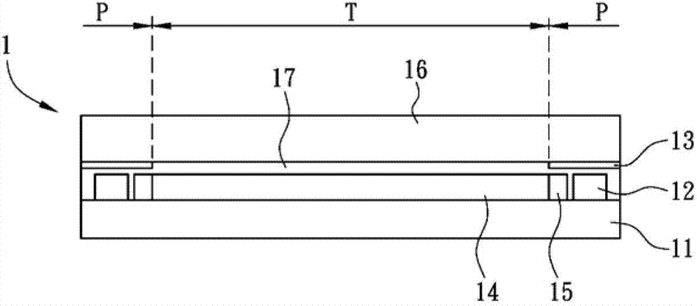
Figure 1A to Fig. 1 C is the side schematic view of the contact panel of preferred embodiment of the present invention;
The schematic top plan view of the contact panel that Fig. 2 A to Fig. 2 G is preferred embodiment of the present invention; And
The side schematic view of the electronic installation being assembled by contact panel that Fig. 3 A and Fig. 3 B are preferred embodiment of the present invention.
Main element symbol description
1,1a~1i, 32: contact panel
10,320: antenna traces pin
11: the first base materials
12: antenna element
13: decorative layer
14: sensing cell
15: sense line
16: the second base materials
17: bonding material
18: aerial signal circuit
19: sense line pin
21: outside wire rod
22: flexible printed wiring board
3a, 3b: electronic installation
31: electronic module
311: display panel
312: circuit board
33: radio-frequency module
34: wire rod
P: surrounding zone
T: touch-control input field
Embodiment
Hereinafter with reference to relevant drawings, a kind of contact panel and electronic installation thereof according to preferred embodiment of the present invention are described, wherein identical element is illustrated the reference marks with identical.
Figure 1A to Fig. 1 C is the side schematic view of the contact panel 1 of preferred embodiment of the present invention, as shown in Figure 1A, a contact panel 1 comprises one first base material 11, an antenna element 12, a decorative layer 13, a sensing cell 14, a sense line 15 and one second base material 16.Wherein, the material of antenna element 12 comprises the alloy of silver, copper, nickel, titanium or above-mentioned material.
The first base material 11 definition have a touch-control input field T and a surrounding zone P, and wherein surrounding zone P is positioned at by the T of touch-control input field, and antenna element 12 is positioned at surrounding zone P, and decorative layer 13 is positioned at surrounding zone P and covers antenna element 12.
Sensing cell 14 is formed on the first base material 11 and is positioned at touch-control input field T, and sense line 15 is formed on the first base material 11 and is positioned at surrounding zone P, and is covered and connected sensing cell 14 by decorative layer 13.
The second base material 16 and the first base material 11 assemblings, antenna element 12, decorative layer 13, sensing cell 14 and sense line 15 are between the first base material 11 and the second base material 16.For instance, a jointing material 17 is in conjunction with the second base material 16 and the first base material 11, and bonding material 17 is for example optical cement, and jointing material 17 can directly or indirectly be coated on the second base material 16 and the first base material 11.
For instance, the second base material 16 is not laid with conducting wire or circuit, for example, as the circuit of touch-control sensor, the circuit of connection touch-control sensor.The second base material 16 can say simple protection material, and it normally covers mirror (cover lens).The normally transparent substrate of the first base material 11, its material is for example glass or plastic cement, only has the first base material 11 to be just laid with circuit in whole contact panel, such contact panel can say the contact panel of monobasal.
Sensing cell 14 can patterned processing and is defined touch-control sensing circuit, and its material is for example tin indium oxide (Indium tin oxide, ITO), and the material of decorative layer 13 is for example insulating material.For instance, sensing cell 14 defines and has a plurality of wires as touch-control sensing circuit on the T of the touch-control input field of the first base material 11, and 13, the not decorated layer of these circuits covers.
In Figure 1A, antenna element 12 is arranged on the first base material 11, and decorative layer 13 is arranged at an inside surface of the second base material 16, covers antenna element 12 and sense line 15 simultaneously.Decorative layer 13 is not arranged on the first base material 11, it can first be formed on the inside surface of the second base material 16, after treating that antenna element 12, sensing cell 14 and sense line 15 have also been arranged on the inside surface of the first base material 11, recycling jointing material 17 is bonding by the inside surface of the second base material 16 and the first base material 11.
In Figure 1B, decorative layer 13 is not arranged on the second base material 16 but is arranged in antenna element 12 and sense line 15, antenna element 12 is arranged on the first base material 11, after antenna element 12, decorative layer 13, sensing cell 14 and sense line 15 have been arranged on the inside surface of the first base material 11, recycling jointing material 17 is bonding by the inside surface of the second base material 16 and the first base material 11.
In Fig. 1 C, decorative layer 13 is arranged at an inside surface of the second base material 16, antenna element 12 is arranged on decorative layer 13, after treating that sensing cell 14 and sense line 15 have also been arranged on the inside surface of the first base material 11, recycling jointing material 17 is bonding by the inside surface of the second base material 16 and the first base material 11.
In Figure 1A to Fig. 1 C, the second base material 16 is normally designed to the outside of whole device, and user operates contact panel from outside, therefore, from outside, it seems, decorative layer 13 all can cover antenna element 12 and sense line 15, these elements visually can not exposed, thus comparatively attractive in appearance.
In addition, in Figure 1A and Figure 1B, also can be provided with the elements such as aerial signal circuit and sense line pin on the first base material 11, relevant embodiment will be in following explanation.
The schematic top plan view of the contact panel that Fig. 2 A to Fig. 2 G is preferred embodiment of the present invention, as shown in Fig. 2 A to Fig. 2 G, for the element that allows decorative layer 13 hide can be known and show on figure, therefore decorative layer 13 is only drawn in profile line part in figure, the right-hand part of contact panel 1c~1i specially do not show decorative layer 13.
In addition, contact panel 1c~1i can only have a base material, and decorative layer 13 tops arrange without another base material.In addition, contact panel 1c~1i also can have two base materials, and decorative layer 13 tops also have another base material setting.No matter have or not, another base material is set, in diagram, also omits and draw another base material.
In Fig. 2 A to Fig. 2 C, contact panel 1c~1e also comprises aerial signal circuit 18, antenna traces pin 10 and sense line pin 19.Sense line pin 19 is formed on the first base material 11 and is positioned at surrounding zone P, it connects sense line 15, aerial signal circuit 18 is positioned at surrounding zone P and is covered by decorative layer 13, antenna traces pin 10 is formed on the first base material 11 and is positioned at surrounding zone P, and aerial signal circuit 18 connects antenna element 12 and antenna traces pin 10.For instance, aerial signal circuit 18 is formed on the first base material 11, and antenna element 12 is arranged on the first base material 11.
For instance, antenna traces pin 10 is covered by decorative layer 13, and the perforation by the first base material 11 is connected directly to aerial signal circuit 18.Sense line pin 19 is covered by decorative layer 13, and the perforation by the first base material 11 is connected directly to sense line 15.
In Fig. 2 A, sense line pin 19 is connected to an outside wire rod 21, and outside wire rod 21 is for example flexible printed wiring board (Flexible Printed Circuit Board, FPC) 22, and antenna traces pin 10 is connected to another outside wire rod.
In Fig. 2 B, sense line pin 19 is connected to same outside wire rod with antenna traces pin 10, for example, be connected to flexible printed wiring board.
In Fig. 2 C, the pin of antenna element 12 can directly contact and be connected to antenna traces pin 10.
In Fig. 2 D, antenna element 12 is connected directly to an outside wire rod 21 by the perforation of the first base material 11.Or antenna element 12 extends along the side of the first base material 11, and is connected with outside wire rod on the side of the first base material 11.
Please refer to again shown in Fig. 2 E to Fig. 2 G, it is the enforcement aspect of not using aerial signal circuit 18.As shown in Figure 2 E, between antenna element 12 and antenna traces pin 10, by aerial signal circuit 18, be not connected, and by antenna traces pin 10 by the perforation of the first base material 11, directly couple antenna element 12 and for example radio-frequency module.Again as shown in Figure 2 F, because the first base material 11 is in side hollow out, for being set, antenna element 12 embeds setting, therefore the right side that antenna traces pin 10 can directly be exposed by antenna element 12 directly couples for example radio-frequency module by antenna element 12.Again as shown in Figure 2 G, certainly, in the structure shown in similar Fig. 2 F, antenna traces pin 10 also can directly couple for example radio-frequency module by antenna element 12 by the perforation of the first base material 11.
In the above description, contact panel 1~1i is an electric resistance touch-control panel or a capacitance type touch-control panel, and capacitance type touch-control panel is for example projected capacitive touch panel.In addition, between antenna element 12 and aerial signal circuit 18, there is at least above interval of 0.5mm, thereby avoid phase mutual interference.Whether again, the thickness of antenna element 12 can be 10um to 30um, and can be arranged on the optional position of surrounding zone P, only will consider to cover by 13, decorated layer, other are non-limiting person.Therefore the magnitude setting of antenna element 12 and corresponding contact and circuit is not limited with one group certainly, and the demand of optical signal transmission, can for two, three or more.
The side schematic view of the electronic installation being assembled by contact panel that Fig. 3 A and Fig. 3 B are preferred embodiment of the present invention, as shown in Fig. 3 A and Fig. 3 B, electronic installation 3a, 3b comprise an electronic module 31, contact panel 32 and a radio-frequency module 33, contact panel 32 and electronic module 31 assemblings, radio-frequency module 33 couples the antenna element of contact panel 32.Contact panel 32 can be the contact panel 1~1i of previous embodiment, therefore the details of contact panel 32 does not repeat them here.
Electronic module is that for example display panel, motherboard or other possess the electronic component of specific function.Display panel is such as being display panels or organic LED panel etc.Motherboard is the circuit board that is provided with integrated circuit and is furnished with circuit, and it can provide the function of certain operations or processing, and integrated circuit is for example processor or memory body, on motherboard, separately can be provided with the elements such as electric capacity or resistance.
In Fig. 3 A, electronic module 31 comprises a display panel 311 and a circuit board 312, and the display surface of display panel 311 is towards the first base material of contact panel 32, and the second base material of contact panel 32 is positioned at outside and can be used as protective.It is other that radio-frequency module 33 can be arranged at circuit board 312, and directly contact with the antenna traces pin 320 of the antenna element of contact panel 32.As for, antenna traces pin 320 can be connected with antenna element by aforesaid aerial signal circuit on first substrate, or directly the perforation by first substrate is connected with antenna element.
In Fig. 3 B, radio-frequency module 33 is to be connected with the antenna traces pin 320 of contact panel 32 by a wire rod 34.Certainly, antenna traces pin 320 can be directly by boring a hole or being connected with antenna element by aerial signal circuit, and the present invention does not limit in this.
Because antenna element is integrated in contact panel in the outer part, except can more simplifying the volume of electronic installation, also have good transmitting-receiving ability concurrently.
In sum, in contact panel of the present invention and electronic installation thereof, antenna element is integrated in the middle of contact panel, therefore can allow electronic installation save additionally arranges the space of antenna and has good receiving and transmitting signal quality concurrently, the decorated layer of antenna covers again, therefore antenna visually there is no the anxiety of exposing, thereby make contact panel comparatively attractive in appearance.
The foregoing is only illustrative, but not be restricted person.Anyly do not depart from spirit of the present invention and category, and the equivalent modifications that it is carried out or change all should be contained in appended claim.
Claims (13)
1. a contact panel, comprising:
The first base material, definition has touch-control input field and surrounding zone, and wherein this surrounding zone is positioned at by this touch-control input field;
Antenna element, is positioned at this surrounding zone; And
Decorative layer, is positioned at this surrounding zone, covers this Anneta module.
2. contact panel as claimed in claim 1, also comprises:
The second base material, with this first base material assembling, this antenna element and this decorative layer are between this first base material and this second base material.
3. contact panel as claimed in claim 1, also comprises:
Sensing cell, is formed on this first base material and is positioned at this touch-control input field; And
Sense line, is formed on this first base material and is positioned at this surrounding zone, by this decorative layer, is covered and is connected this sensing cell.
4. contact panel as claimed in claim 1, also comprises:
Aerial signal circuit, is positioned at this surrounding zone and is covered by this decorative layer, connects this antenna element.
5. contact panel as claimed in claim 4, wherein this aerial signal circuit is formed on this first base material, and this antenna element is arranged on this first base material.
6. contact panel as claimed in claim 5, also comprises:
Antenna traces pin, is formed on this first base material and is positioned at this surrounding zone, connects this aerial signal circuit.
7. contact panel as claimed in claim 6, wherein this antenna traces pin is covered by this decorative layer, and the perforation by this first base material is connected directly to this aerial signal circuit.
8. contact panel as claimed in claim 6, also comprises:
Sense line pin, is formed on this first base material and is positioned at this surrounding zone, is connected to same outside wire rod with this antenna traces pin.
9. contact panel as claimed in claim 6, also comprises:
Sense line pin, is formed on this first base material and is positioned at this surrounding zone, is connected to respectively two outside wire rods with this antenna traces pin.
10. contact panel as claimed in claim 1, wherein this antenna element is connected directly to an outside wire rod by a perforation of this first base material.
11. contact panels as claimed in claim 1, also comprise:
Antenna traces pin, by this antenna element of perforation connection of this first base material.
12. contact panels as claimed in claim 1, also comprise:
Antenna traces pin, this antenna element embeds this surrounding zone of this first base material, and this antenna traces pin couples the side that this antenna element exposes.
13. 1 kinds of electronic installations, comprising:
Electronic module;
As claim 1 to 12 contact panel of wherein, itself and this electronic module assembling; And
Radio-frequency module, couples this antenna element of this contact panel.
Applications Claiming Priority (2)
| Application Number | Priority Date | Filing Date | Title |
|---|---|---|---|
| TW101129247 | 2012-08-13 | ||
| TW101129247A TWI475439B (en) | 2012-08-13 | 2012-08-13 | Touch panel and electronic device thereof |
Publications (1)
| Publication Number | Publication Date |
|---|---|
| CN103593084A true CN103593084A (en) | 2014-02-19 |
Family
ID=50065837
Family Applications (1)
| Application Number | Title | Priority Date | Filing Date |
|---|---|---|---|
| CN201310196574.6A Pending CN103593084A (en) | 2012-08-13 | 2013-05-24 | Touch panel and electronic device thereof |
Country Status (3)
| Country | Link |
|---|---|
| US (1) | US9274627B2 (en) |
| CN (1) | CN103593084A (en) |
| TW (1) | TWI475439B (en) |
Cited By (5)
| Publication number | Priority date | Publication date | Assignee | Title |
|---|---|---|---|---|
| CN106484163A (en) * | 2015-08-28 | 2017-03-08 | 介面光电股份有限公司 | Metal grid touch control film with antenna module and embedded touch control display device |
| TWI588700B (en) * | 2015-05-26 | 2017-06-21 | 宸鴻科技(廈門)有限公司 | Touch-sensitive device |
| CN107209604A (en) * | 2015-07-03 | 2017-09-26 | 日本写真印刷株式会社 | And the contact panel provided with antenna |
| CN109213272A (en) * | 2017-06-30 | 2019-01-15 | 纬创资通股份有限公司 | electronic device |
| CN112684927A (en) * | 2019-10-18 | 2021-04-20 | 昆山国显光电有限公司 | Touch display panel and manufacturing method thereof |
Families Citing this family (9)
| Publication number | Priority date | Publication date | Assignee | Title |
|---|---|---|---|---|
| TWI475439B (en) * | 2012-08-13 | 2015-03-01 | Wistron Corp | Touch panel and electronic device thereof |
| CN105511658A (en) | 2014-10-09 | 2016-04-20 | 中兴通讯股份有限公司 | Touch screen and terminal |
| JP6348874B2 (en) * | 2015-05-19 | 2018-06-27 | 富士フイルム株式会社 | Touch sensor panel |
| JP6030276B1 (en) * | 2015-07-03 | 2016-11-24 | 日本写真印刷株式会社 | Touch panel with antenna |
| JP6672881B2 (en) * | 2016-02-24 | 2020-03-25 | 凸版印刷株式会社 | Touch panel and information processing device |
| WO2018147109A1 (en) * | 2017-02-10 | 2018-08-16 | アルプス電気株式会社 | Display device |
| US11275473B2 (en) * | 2019-06-13 | 2022-03-15 | Samsung Display Co., Ltd. | Display panel and display device including the same |
| KR102915058B1 (en) * | 2019-10-08 | 2026-01-21 | 삼성디스플레이 주식회사 | Display apparatus |
| CN114327146B (en) * | 2021-12-31 | 2023-10-20 | 云谷(固安)科技有限公司 | Display panels and display devices |
Citations (3)
| Publication number | Priority date | Publication date | Assignee | Title |
|---|---|---|---|---|
| CN102124428A (en) * | 2008-08-21 | 2011-07-13 | 日本写真印刷株式会社 | Protective panel with excellent surface flatness and touch input function, and electronic device having the protective panel |
| TWM416105U (en) * | 2011-03-18 | 2011-11-11 | Auden Technology Corp | Touch structure and touch panel with antenna function |
| CN202221808U (en) * | 2011-07-27 | 2012-05-16 | 青岛长弓塑模有限公司 | Panel possessing externally-mounted type antenna |
Family Cites Families (3)
| Publication number | Priority date | Publication date | Assignee | Title |
|---|---|---|---|---|
| KR101342731B1 (en) * | 2007-01-04 | 2013-12-19 | 니폰샤신인사츠가부시키가이샤 | Protective panel having touch panel function |
| TWM425335U (en) * | 2011-12-02 | 2012-03-21 | Luminous Optical Technology Co Ltd | Touch panel structure with antenna |
| TWI475439B (en) * | 2012-08-13 | 2015-03-01 | Wistron Corp | Touch panel and electronic device thereof |
-
2012
- 2012-08-13 TW TW101129247A patent/TWI475439B/en active
-
2013
- 2013-05-24 CN CN201310196574.6A patent/CN103593084A/en active Pending
- 2013-05-28 US US13/902,990 patent/US9274627B2/en active Active
Patent Citations (3)
| Publication number | Priority date | Publication date | Assignee | Title |
|---|---|---|---|---|
| CN102124428A (en) * | 2008-08-21 | 2011-07-13 | 日本写真印刷株式会社 | Protective panel with excellent surface flatness and touch input function, and electronic device having the protective panel |
| TWM416105U (en) * | 2011-03-18 | 2011-11-11 | Auden Technology Corp | Touch structure and touch panel with antenna function |
| CN202221808U (en) * | 2011-07-27 | 2012-05-16 | 青岛长弓塑模有限公司 | Panel possessing externally-mounted type antenna |
Cited By (9)
| Publication number | Priority date | Publication date | Assignee | Title |
|---|---|---|---|---|
| TWI588700B (en) * | 2015-05-26 | 2017-06-21 | 宸鴻科技(廈門)有限公司 | Touch-sensitive device |
| CN107209604A (en) * | 2015-07-03 | 2017-09-26 | 日本写真印刷株式会社 | And the contact panel provided with antenna |
| US9904430B2 (en) | 2015-07-03 | 2018-02-27 | Nissha Co., Ltd. | Antenna-equipped touch panel having an opening between antenna pattern and detection pattern |
| CN107209604B (en) * | 2015-07-03 | 2020-12-29 | 日本写真印刷株式会社 | touch panel with antenna |
| CN106484163A (en) * | 2015-08-28 | 2017-03-08 | 介面光电股份有限公司 | Metal grid touch control film with antenna module and embedded touch control display device |
| CN109213272A (en) * | 2017-06-30 | 2019-01-15 | 纬创资通股份有限公司 | electronic device |
| CN109213272B (en) * | 2017-06-30 | 2020-08-14 | 纬创资通股份有限公司 | electronic device |
| CN112684927A (en) * | 2019-10-18 | 2021-04-20 | 昆山国显光电有限公司 | Touch display panel and manufacturing method thereof |
| CN112684927B (en) * | 2019-10-18 | 2022-10-21 | 昆山国显光电有限公司 | Touch display panel and manufacturing method thereof |
Also Published As
| Publication number | Publication date |
|---|---|
| US9274627B2 (en) | 2016-03-01 |
| TW201407438A (en) | 2014-02-16 |
| US20140043261A1 (en) | 2014-02-13 |
| TWI475439B (en) | 2015-03-01 |
Similar Documents
| Publication | Publication Date | Title |
|---|---|---|
| CN103593084A (en) | Touch panel and electronic device thereof | |
| US8946578B2 (en) | Touch panel and a manufacturing method thereof | |
| TWI602091B (en) | Touch module with transparent antenna and touch display apparatus using same | |
| EP2090967B1 (en) | Capacitive touch panel | |
| US9239653B2 (en) | Touch panel and method of fabricating the same | |
| CN108646946B (en) | Flexible touch panel, manufacturing method thereof and flexible touch display | |
| KR101138138B1 (en) | Translucent touch screens including invisible electronic component connections | |
| EP2597551A2 (en) | Touch panel having border without color difference and manufacturing method thereof | |
| US20130257791A1 (en) | Capacitive touch screen and manufacturing method thereof | |
| US10545596B2 (en) | Touch display device | |
| TWM483477U (en) | Touch panel | |
| CN103186274B (en) | Contact panel and preparation method thereof | |
| CN104216551A (en) | Touch control panel | |
| CN109375822B (en) | Touch screen, touch screen and mobile terminal | |
| US20140145971A1 (en) | TOUCH Panel | |
| KR101418159B1 (en) | Touch panel | |
| CN106557191A (en) | Touch display device with fingerprint identification function and fingerprint identification module thereof | |
| TWI472977B (en) | Touch panel and method of manufacturing same | |
| TWI471786B (en) | Touch panel | |
| CN107589866A (en) | Flexible touch sensing and contact panel | |
| CN103576951A (en) | Touch panel, manufacturing method and display device of touch panel | |
| CN207586885U (en) | A kind of flexible bendable CTP and electronic equipment | |
| CN207819880U (en) | Flexible circuit board, biological information sensing module and electronic equipment | |
| CN202584060U (en) | Touch panel | |
| CN203133801U (en) | Touch panel |
Legal Events
| Date | Code | Title | Description |
|---|---|---|---|
| C06 | Publication | ||
| PB01 | Publication | ||
| SE01 | Entry into force of request for substantive examination | ||
| SE01 | Entry into force of request for substantive examination | ||
| RJ01 | Rejection of invention patent application after publication | ||
| RJ01 | Rejection of invention patent application after publication |
Application publication date: 20140219 |