CN103258770A - Method of manufacturing semiconductor device and method of manufacturing electronic device - Google Patents
Method of manufacturing semiconductor device and method of manufacturing electronic device Download PDFInfo
- Publication number
- CN103258770A CN103258770A CN2013100487662A CN201310048766A CN103258770A CN 103258770 A CN103258770 A CN 103258770A CN 2013100487662 A CN2013100487662 A CN 2013100487662A CN 201310048766 A CN201310048766 A CN 201310048766A CN 103258770 A CN103258770 A CN 103258770A
- Authority
- CN
- China
- Prior art keywords
- film
- adhesive layer
- layer
- semiconductor element
- substrate
- Prior art date
- Legal status (The legal status is an assumption and is not a legal conclusion. Google has not performed a legal analysis and makes no representation as to the accuracy of the status listed.)
- Granted
Links
Images


Classifications
-
- H—ELECTRICITY
- H10—SEMICONDUCTOR DEVICES; ELECTRIC SOLID-STATE DEVICES NOT OTHERWISE PROVIDED FOR
- H10W—GENERIC PACKAGES, INTERCONNECTIONS, CONNECTORS OR OTHER CONSTRUCTIONAL DETAILS OF DEVICES COVERED BY CLASS H10
- H10W74/00—Encapsulations, e.g. protective coatings
- H10W74/01—Manufacture or treatment
- H10W74/019—Manufacture or treatment using temporary auxiliary substrates
-
- H—ELECTRICITY
- H10—SEMICONDUCTOR DEVICES; ELECTRIC SOLID-STATE DEVICES NOT OTHERWISE PROVIDED FOR
- H10P—GENERIC PROCESSES OR APPARATUS FOR THE MANUFACTURE OR TREATMENT OF DEVICES COVERED BY CLASS H10
- H10P72/00—Handling or holding of wafers, substrates or devices during manufacture or treatment thereof
- H10P72/70—Handling or holding of wafers, substrates or devices during manufacture or treatment thereof for supporting or gripping
- H10P72/74—Handling or holding of wafers, substrates or devices during manufacture or treatment thereof for supporting or gripping using temporarily an auxiliary support
-
- H—ELECTRICITY
- H10—SEMICONDUCTOR DEVICES; ELECTRIC SOLID-STATE DEVICES NOT OTHERWISE PROVIDED FOR
- H10W—GENERIC PACKAGES, INTERCONNECTIONS, CONNECTORS OR OTHER CONSTRUCTIONAL DETAILS OF DEVICES COVERED BY CLASS H10
- H10W70/00—Package substrates; Interposers; Redistribution layers [RDL]
- H10W70/01—Manufacture or treatment
- H10W70/05—Manufacture or treatment of insulating or insulated package substrates, or of interposers, or of redistribution layers
- H10W70/08—Manufacture or treatment of insulating or insulated package substrates, or of interposers, or of redistribution layers by depositing layers on the chip or wafer, e.g. "chip-first" RDLs
- H10W70/09—Manufacture or treatment of insulating or insulated package substrates, or of interposers, or of redistribution layers by depositing layers on the chip or wafer, e.g. "chip-first" RDLs extending onto an encapsulation that laterally surrounds the chip or wafer, e.g. fan-out wafer level package [FOWLP] RDLs
-
- H—ELECTRICITY
- H10—SEMICONDUCTOR DEVICES; ELECTRIC SOLID-STATE DEVICES NOT OTHERWISE PROVIDED FOR
- H10W—GENERIC PACKAGES, INTERCONNECTIONS, CONNECTORS OR OTHER CONSTRUCTIONAL DETAILS OF DEVICES COVERED BY CLASS H10
- H10W70/00—Package substrates; Interposers; Redistribution layers [RDL]
- H10W70/60—Insulating or insulated package substrates; Interposers; Redistribution layers
-
- H—ELECTRICITY
- H10—SEMICONDUCTOR DEVICES; ELECTRIC SOLID-STATE DEVICES NOT OTHERWISE PROVIDED FOR
- H10W—GENERIC PACKAGES, INTERCONNECTIONS, CONNECTORS OR OTHER CONSTRUCTIONAL DETAILS OF DEVICES COVERED BY CLASS H10
- H10W72/00—Interconnections or connectors in packages
- H10W72/01—Manufacture or treatment
- H10W72/0198—Manufacture or treatment batch processes
-
- H—ELECTRICITY
- H10—SEMICONDUCTOR DEVICES; ELECTRIC SOLID-STATE DEVICES NOT OTHERWISE PROVIDED FOR
- H10P—GENERIC PROCESSES OR APPARATUS FOR THE MANUFACTURE OR TREATMENT OF DEVICES COVERED BY CLASS H10
- H10P72/00—Handling or holding of wafers, substrates or devices during manufacture or treatment thereof
- H10P72/70—Handling or holding of wafers, substrates or devices during manufacture or treatment thereof for supporting or gripping
- H10P72/74—Handling or holding of wafers, substrates or devices during manufacture or treatment thereof for supporting or gripping using temporarily an auxiliary support
- H10P72/7412—Handling or holding of wafers, substrates or devices during manufacture or treatment thereof for supporting or gripping using temporarily an auxiliary support the auxiliary support including means facilitating the separation of a device or wafer from the auxiliary support
-
- H—ELECTRICITY
- H10—SEMICONDUCTOR DEVICES; ELECTRIC SOLID-STATE DEVICES NOT OTHERWISE PROVIDED FOR
- H10P—GENERIC PROCESSES OR APPARATUS FOR THE MANUFACTURE OR TREATMENT OF DEVICES COVERED BY CLASS H10
- H10P72/00—Handling or holding of wafers, substrates or devices during manufacture or treatment thereof
- H10P72/70—Handling or holding of wafers, substrates or devices during manufacture or treatment thereof for supporting or gripping
- H10P72/74—Handling or holding of wafers, substrates or devices during manufacture or treatment thereof for supporting or gripping using temporarily an auxiliary support
- H10P72/744—Details of chemical or physical process used for separating the auxiliary support from a device or a wafer
-
- H—ELECTRICITY
- H10—SEMICONDUCTOR DEVICES; ELECTRIC SOLID-STATE DEVICES NOT OTHERWISE PROVIDED FOR
- H10W—GENERIC PACKAGES, INTERCONNECTIONS, CONNECTORS OR OTHER CONSTRUCTIONAL DETAILS OF DEVICES COVERED BY CLASS H10
- H10W72/00—Interconnections or connectors in packages
- H10W72/20—Bump connectors, e.g. solder bumps or copper pillars; Dummy bumps; Thermal bumps
- H10W72/241—Dispositions, e.g. layouts
-
- H—ELECTRICITY
- H10—SEMICONDUCTOR DEVICES; ELECTRIC SOLID-STATE DEVICES NOT OTHERWISE PROVIDED FOR
- H10W—GENERIC PACKAGES, INTERCONNECTIONS, CONNECTORS OR OTHER CONSTRUCTIONAL DETAILS OF DEVICES COVERED BY CLASS H10
- H10W72/00—Interconnections or connectors in packages
- H10W72/90—Bond pads, in general
- H10W72/941—Dispositions of bond pads
- H10W72/9413—Dispositions of bond pads on encapsulations
-
- H—ELECTRICITY
- H10—SEMICONDUCTOR DEVICES; ELECTRIC SOLID-STATE DEVICES NOT OTHERWISE PROVIDED FOR
- H10W—GENERIC PACKAGES, INTERCONNECTIONS, CONNECTORS OR OTHER CONSTRUCTIONAL DETAILS OF DEVICES COVERED BY CLASS H10
- H10W74/00—Encapsulations, e.g. protective coatings
- H10W74/01—Manufacture or treatment
- H10W74/014—Manufacture or treatment using batch processing
-
- H—ELECTRICITY
- H10—SEMICONDUCTOR DEVICES; ELECTRIC SOLID-STATE DEVICES NOT OTHERWISE PROVIDED FOR
- H10W—GENERIC PACKAGES, INTERCONNECTIONS, CONNECTORS OR OTHER CONSTRUCTIONAL DETAILS OF DEVICES COVERED BY CLASS H10
- H10W74/00—Encapsulations, e.g. protective coatings
- H10W74/10—Encapsulations, e.g. protective coatings characterised by their shape or disposition
- H10W74/111—Encapsulations, e.g. protective coatings characterised by their shape or disposition the semiconductor body being completely enclosed
- H10W74/114—Encapsulations, e.g. protective coatings characterised by their shape or disposition the semiconductor body being completely enclosed by a substrate and the encapsulations
- H10W74/117—Encapsulations, e.g. protective coatings characterised by their shape or disposition the semiconductor body being completely enclosed by a substrate and the encapsulations the substrate having spherical bumps for external connection
-
- H—ELECTRICITY
- H10—SEMICONDUCTOR DEVICES; ELECTRIC SOLID-STATE DEVICES NOT OTHERWISE PROVIDED FOR
- H10W—GENERIC PACKAGES, INTERCONNECTIONS, CONNECTORS OR OTHER CONSTRUCTIONAL DETAILS OF DEVICES COVERED BY CLASS H10
- H10W90/00—Package configurations
Landscapes
- Encapsulation Of And Coatings For Semiconductor Or Solid State Devices (AREA)
- Adhesive Tapes (AREA)
- Engineering & Computer Science (AREA)
- Manufacturing & Machinery (AREA)
- Dicing (AREA)
Abstract
Description
技术领域technical field
本文中所讨论的实施例涉及一种制造半导体装置的方法和制造电子装置的方法。Embodiments discussed herein relate to a method of manufacturing a semiconductor device and a method of manufacturing an electronic device.
背景技术Background technique
晶片级封装(wafer level package,WLP)被认为是包含诸如裸芯片的半导体元件(电子部件)的半导体封装(半导体装置)的示例。WLP也被称为晶片级芯片尺寸封装(wafer-level chip size package,WL-CSP)或晶片芯片尺寸封装(wafer chip size package,W-CSP)。WLP使位于裸芯片端部的端子能够在芯片区域内(即,扇入)被重新布置。此外,因为随着裸芯片的端子数量增加难以在芯片区域内对端子进行重新布置,所以使端子能够在芯片区域之外(即,扇出)重新布置的WLP也正在被开发。A wafer level package (WLP) is considered as an example of a semiconductor package (semiconductor device) including a semiconductor element (electronic part) such as a bare chip. WLP is also known as wafer-level chip size package (WL-CSP) or wafer chip size package (W-CSP). WLP enables terminals located at the ends of the die to be rearranged within the chip area (ie, fan-in). Furthermore, since it is difficult to rearrange terminals within a chip area as the number of terminals of a bare chip increases, WLPs that enable rearrangement of terminals outside the chip area (ie, fan-out) are also being developed.
在已知的制造这种半导体封装的方法中,半导体元件附着到由粘接性材料组成的被设置在支承构件上的粘接片或粘接层,并用树脂密封以形成伪晶片;将伪晶片与粘接层分离;布线层形成在伪晶片的与粘接层分离的表面上;以及切割伪晶片。由此,获得了单独的半导体封装。在该制造方法中,通过例如紫外线照射、化学处理或加热处理来降低粘接层的粘接性来将伪晶片与粘接层分离。In a known method of manufacturing such a semiconductor package, a semiconductor element is attached to an adhesive sheet or an adhesive layer composed of an adhesive material provided on a support member and sealed with a resin to form a dummy wafer; the dummy wafer separating from the adhesive layer; forming a wiring layer on the surface of the dummy wafer separated from the adhesive layer; and dicing the dummy wafer. Thereby, individual semiconductor packages are obtained. In this manufacturing method, the dummy wafer is separated from the adhesive layer by reducing the adhesiveness of the adhesive layer by, for example, ultraviolet irradiation, chemical treatment, or heat treatment.
在另一种已知的方法中,粘接层由下述粘接性材料构成:其具有相对于用于密封半导体元件的树脂有效的脱模性(release property)和溶剂的溶解度。In another known method, the adhesive layer is composed of an adhesive material having effective release properties and solubility in solvents with respect to the resin used to seal the semiconductor element.
如下是相关技术的示例:美国专利第7202107B2号的说明书、日本专利第4403631号和日本特开专利公开第2002-299500号。Examples of related art are as follows: specification of US Patent No. 7202107B2, Japanese Patent No. 4403631, and Japanese Laid-Open Patent Publication No. 2002-299500.
在将形成在粘接层上的伪晶片(基片)与粘接层分离的方法中,可对粘接层进行紫外线照射、化学处理或加热处理,以降低粘接层的粘接性。In the method of separating the dummy wafer (substrate) formed on the adhesive layer from the adhesive layer, the adhesive layer may be subjected to ultraviolet irradiation, chemical treatment, or heat treatment to reduce the adhesiveness of the adhesive layer.
一旦粘接层的粘接性降低,无论如何都难以重复使用粘接层,并且每次形成伪晶片时使用新的粘接层。因此,难以降低用于制造半导体装置(半导体封装)的工时和成本。此外,使用如上面描述那样制造的半导体装置,也会增加电子装置的成本。Once the adhesiveness of the adhesive layer decreases, it is difficult to reuse the adhesive layer anyway, and a new adhesive layer is used every time a dummy wafer is formed. Therefore, it is difficult to reduce man-hours and costs for manufacturing semiconductor devices (semiconductor packages). Furthermore, using a semiconductor device fabricated as described above also increases the cost of the electronic device.
发明内容Contents of the invention
在一个方面,本发明的实施例提供了用于降低工时和成本的半导体装置和电子装置的制造方法。In one aspect, embodiments of the present invention provide a method of manufacturing a semiconductor device and an electronic device for reducing man-hours and costs.
根据本发明的一个方面,一种制造半导体装置的方法包括:在支承构件上设置第一粘接层;在该第一粘接层上设置膜;在该膜上布置半导体元件;在布置有半导体元件的膜上设置树脂层,并在膜上形成包括半导体元件和树脂层的基片;以及使膜和基片与第一粘接层分离。According to an aspect of the present invention, a method of manufacturing a semiconductor device includes: providing a first adhesive layer on a supporting member; providing a film on the first adhesive layer; disposing a semiconductor element on the film; providing a resin layer on the film of the element, and forming a substrate including the semiconductor element and the resin layer on the film; and separating the film and the substrate from the first adhesive layer.
本发明的目的和优点将通过在权利要求中具体指出的要素和组合得以实现和获得。The objects and advantages of the invention will be realized and attained by means of the elements and combinations particularly pointed out in the claims.
应该被理解的是,前面的一般性描述和以下的详细描述对于所要求保护的本发明都是示例性和解释性的,而不是限制性的。It is to be understood that both the foregoing general description and the following detailed description are exemplary and explanatory, and not restrictive, of the invention as claimed.
附图说明Description of drawings
图1A至图1C示出了制造半导体装置的方法的示例(第1部分);1A to 1C illustrate an example of a method of manufacturing a semiconductor device (Part 1);
图2A至图2D示出了制造半导体装置的方法的示例(第2部分);2A to 2D illustrate an example of a method of manufacturing a semiconductor device (Part 2);
图3A至图3D示出了另一种制造半导体装置的方法;3A to 3D illustrate another method of manufacturing a semiconductor device;
图4A和图4B示出了粘接层的配置的示例;Figure 4A and Figure 4B show the example of the configuration of adhesive layer;
图5A和图5B示出了形成粘接层的方法的示例(第1部分);5A and 5B show an example of a method of forming an adhesive layer (Part 1);
图6A和图6B示出了形成粘接层的方法的示例(第2部分);6A and 6B illustrate an example of a method of forming an adhesive layer (Part 2);
图7A和图7B示出了膜的配置的示例;Figures 7A and 7B show examples of membrane configurations;
图8示出了半导体装置的制造过程的示例(第1部分);FIG. 8 shows an example of a manufacturing process of a semiconductor device (Part 1);
图9示出了半导体装置的制造过程的示例(第2部分);FIG. 9 shows an example of a manufacturing process of a semiconductor device (part 2);
图10示出了半导体装置的制造过程的示例(第3部分);FIG. 10 shows an example of a manufacturing process of a semiconductor device (part 3);
图11示出了半导体装置的制造过程的示例(第4部分);FIG. 11 shows an example of a manufacturing process of a semiconductor device (Part 4);
图12示出了半导体装置的制造过程的示例(第5部分);FIG. 12 shows an example of a manufacturing process of a semiconductor device (Part 5);
图13示出了半导体装置的制造过程的示例(第6部分);Figure 13 shows an example of a manufacturing process of a semiconductor device (Part 6);
图14示出了半导体装置的制造过程的示例(第7部分);Figure 14 shows an example of a manufacturing process of a semiconductor device (Part 7);
图15示出了半导体装置的制造过程的示例(第8部分);Figure 15 shows an example of a manufacturing process of a semiconductor device (Part 8);
图16A至图16D示出了半导体装置的制造过程的示例(第9部分);16A to 16D show an example of a manufacturing process of a semiconductor device (Part 9);
图17A至图17D示出了半导体装置的制造过程的示例(第10部分);以及17A to 17D show an example of a manufacturing process of a semiconductor device (Part 10); and
图18示出了电子装置的示例。FIG. 18 shows an example of an electronic device.
具体实施方式Detailed ways
图1A至1C和图2A至2D示出了制造半导体装置的方法的示例。图1A是示出了设置粘接层和膜的示例的相关部分的示意性截面视图。图1B是示出了布置半导体元件的示例的相关部分的示意性截面视图。图1C是示出了设置树脂层(形成伪晶片)的示例的相关部分的示意性截面视图。图2A和2B是示出了同时分离伪晶片和膜的示例的相关部分的示意性截面视图。图2C和2D是示出了分离膜的示例的相关部分的示意性截面视图。1A to 1C and 2A to 2D illustrate an example of a method of manufacturing a semiconductor device. FIG. 1A is a schematic sectional view of a relevant part showing an example in which an adhesive layer and a film are provided. FIG. 1B is a schematic cross-sectional view of a relevant portion showing an example of arranging semiconductor elements. FIG. 1C is a schematic sectional view of a relevant part showing an example in which a resin layer is provided (dummy wafer is formed). 2A and 2B are schematic sectional views of relevant parts showing an example of simultaneously separating a dummy wafer and a film. 2C and 2D are schematic cross-sectional views showing relevant parts of an example of a separation membrane.
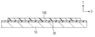
当制造半导体装置时,首先,如图1A所示,粘接层20被设置在支承构件10上,并且膜(粘接膜)100被设置在粘接层20上。支承构件10可以由半导体(例如,硅)基片、玻璃基片、金属(例如,不锈钢)基片、陶瓷基片等制成。粘接层20和膜100可以由粘接性树脂制成,该粘接性树脂诸如为环氧树脂、丙烯酸树脂、聚酰亚胺树脂、硅酮树脂、或聚氨酯树脂。膜100由粘接性和柔性的材料制成。此外,膜100具有与在下面的粘接层20不同的形状(在本文中,示出了膜100在平面视图中的尺寸小于粘接层20在平面视图中的尺寸的示例)。下面将描述粘接层20和膜100的细节。When manufacturing a semiconductor device, first, as shown in FIG. 1A , an
在粘接层20和膜100被设置在支承构件10上之后,作为电子部件的半导体元件30被布置在膜100上,如图1B所示。半导体元件30被附着到膜100,使得设置有电极31的表面(电极表面)30a面向膜100。半导体元件30可以是裸芯片,例如,由诸如硅或砷化镓的半导体材料构成的大规模集成电路(large-scale integrated circuit,LSI)。半导体元件30可以使用倒装芯片接合机、贴装机等被布置在膜100上。After the
图1B仅示出了一个半导体元件30,但是布置在膜100上的半导体元件30可以多于一个。与图1B中所示的配置类似,多个半导体元件30可以被布置在单个膜100上的预定位置处,使得电极表面30a面向粘接层20。FIG. 1B shows only one
在半导体元件30被布置在膜100上之后,树脂层40被设置在膜100上,如图1C所示。树脂层40可以由用于密封半导体元件30的任何非导电性密封树脂材料制成。树脂层40可以包含非导电填料,例如氧化铝、二氧化硅、氢氧化铝、或氮化铝、或包含它们中的至少一种的无机填料。树脂层40通过例如模塑而被设置在膜100上。替选地,树脂层40可以通过用树脂来填充膜100上的半导体元件30周围的框架而设置在膜100上。设置在膜100上的树脂层40通过加热或紫外线照射而被固化。以这种方式,树脂层40被设置在膜100上,并且伪晶片(基片)50被形成在膜100上,在该伪晶片(基片)50中,半导体元件30用树脂层40来密封。After the
树脂层40在此阶段不必被完全固化。正如下面将描述的那样,树脂层40被固化到下面这样的程度就足够了,即伪晶片50在与粘接层20和膜100分离之后能够被拿起(handle),同时保持在晶片状态下。The
在此阶段树脂层40的固化条件(温度条件、紫外线照射条件等)根据树脂层40、粘接层20和膜100的材料来确定,以使得粘接层20和膜100的粘接性被保持。替选地,粘接层20和膜100的材料根据树脂层40的材料和固化条件来确定。The curing conditions (temperature conditions, ultraviolet irradiation conditions, etc.) of the
伪晶片50被形成为在平面视图中具有比膜100更小的尺寸。替选地,在平面视图中具有比伪晶片50更大的尺寸的膜100被预先形成在粘接层20上。膜100具有这样的形状和尺寸,该形状和尺寸使得膜100的至少一部分在平面视图中延伸超出伪晶片50。The
接下来,如图2A和2B所示,膜100和形成在膜100上的伪晶片50同时与粘接层20分离。当膜100和伪晶片50同时与粘接层20分离时,如图2A所示,首先,膜100的没有形成伪晶片50的边缘100a与粘接层20分离。随后,如图2B所示,膜100和伪晶片50一起从先前分离的边缘100a与粘接层20分离。以这种方式,伪晶片50和膜100同时与粘接层20和支承构件10分离。Next, as shown in FIGS. 2A and 2B , the
当同时将伪晶片50和膜100与粘接层20分离时,降低粘接层20的粘接性的处理(诸如紫外线照射、化学处理、或加热处理)可以被省略。在未进行降低粘接层20的粘接性的处理的情况下,如图2A和2B所示,伪晶片50和膜100可以通过使用从边缘100a将膜100与粘接层20分离的方法而同时容易地与粘接层20分离。When the
在伪晶片50和膜100同时与粘接层20分离之后,将膜100与伪晶片50分离,如图2C和2D所示。当膜100与伪晶片50分离时,如图2C所示,首先,膜100的没有形成伪晶片50的边缘100b与伪晶片50分离。随后,如图2D所示,整个膜100从先前分离的边缘100b与伪晶片50分离。通过进行该过程,获得了与支承构件10、粘接层20和膜100分离的伪晶片50。After the
当将膜100与伪晶片50分离时,降低膜100的粘接性的处理(诸如紫外线照射、化学处理或加热处理)可以被省略。在未进行降低膜100的粘接性的处理的情况下,如图2C和2D所示,膜100可以通过使用从边缘100b将膜100与伪晶片50分离的方法而容易地与伪晶片50分离。When separating the
与膜100分离的伪晶片50可以进行加热或紫外线照射,以进一步固化树脂层40。包括被电连接到半导体元件30的电极31的导电部分(过孔、引线等)的布线层(重新布线层)被形成在如此形成的伪晶片50的与膜100分离的表面(即,露出半导体元件30的电极表面30a的表面)上。在布线层形成之后,树脂层40和布线层在半导体元件30周围的位置处被切割,并由此形成了各自包括半导体元件30的单独的半导体装置(半导体封装)。The
现在,将描述制造半导体装置的另一种方法以进行比较。图3A至3C示出了制造半导体装置的另一种方法。图3A是示出了设置粘接层的示例的相关部分的示意性截面视图。图3B是示出了布置半导体元件的示例的相关部分的示意性截面视图。图3C是示出了设置树脂层(形成伪晶片)的示例的相关部分的示意性截面视图。图3D是示出了分离伪晶片的示例的相关部分的示意性截面视图。Now, another method of manufacturing a semiconductor device will be described for comparison. 3A to 3C illustrate another method of manufacturing a semiconductor device. Fig. 3A is a schematic sectional view of a relevant part showing an example in which an adhesive layer is provided. 3B is a schematic cross-sectional view of a relevant portion showing an example of arranging semiconductor elements. 3C is a schematic cross-sectional view of a relevant part showing an example in which a resin layer is provided (dummy wafer is formed). FIG. 3D is a schematic sectional view of a relevant part showing an example of separating a dummy wafer.
在该方法中,首先,如图3A所示,粘接层20被设置在支承构件10上。接下来,如图3B所示,半导体元件30被布置在粘接层20上,使得其电极表面30a面向粘接层20。随后,如图3C所示,树脂层40被设置在其上布置有半导体元件30的粘接层20上。通过固化树脂层40,伪晶片50被形成在粘接层20上。然后,如图3D所示,伪晶片50与粘接层20分离。布线层被形成在伪晶片50的与粘接层20分离的表面上,并且伪晶片50被切割成单独的半导体装置(半导体封装)。In this method, first, as shown in FIG. 3A , the
在该方法中的图3D所示的过程中,当伪晶片50将要与粘接层20分离时,对粘接层20进行例如紫外线照射处理、化学处理、加热处理等以降低粘接层20的粘接性,然后,伪晶片50与粘接层20分离。在这种情况下,已进行紫外线照射、化学处理、加热处理等以降低粘接性的粘接层20难以重复使用。因此,在该方法中,使用过的被降低了粘接性的粘接层20被丢弃,并且每次形成伪晶片50时都使用新的粘接层20。执行降低粘接层20的粘接性的处理以及因而发生的无法重复使用粘接层20,导致了制造伪晶片50的工时和成本的增加以及从伪晶片50生产半导体封装的成本的增加。In the process shown in FIG. 3D in this method, when the
具有低粘接性的粘接层20也可以被预先设置在支承构件10上,并手工将形成在粘接层20上的伪晶片50分离。然而,即使使用这种具有相对低粘接性的粘接层20,从粘接层20分离伪晶片50也是不容易的,因为支承构件10和包含固化的树脂层40的伪晶片50都是刚性和不太可能产生形变的。此外,如果使用具有低粘接性的粘接层20,则其上设置的半导体元件30会由于在通过模塑形成树脂层40时施加的压力或在固化时树脂层40的收缩而产生位移。半导体元件30的位移会在后续过程中形成布线层时导致导电部分和半导体元件30之间的有故障的电连接。The
相比之下,当膜100被设置在伪晶片50和粘接层20之间时,如在图1A至1C所示的方法中,在不降低粘接层20的粘接性的情况下,伪晶片50和膜100可以同时并容易地与粘接层20分离。随后,膜100与伪晶片50分离以得到分离的伪晶片50。In contrast, when the
如已经描述的,伪晶片50可以使用膜100与粘接层20分离,而不执行降低粘接层20的粘接性的处理。因此,变得可以重复使用粘接层20。更具体地,如图1A至1C所示,首先,半导体元件30通过在粘接层20与半导体元件30之间的膜100被布置在支承构件10上的粘接层20上,并且树脂层40被设置在其上以形成第一伪晶片50。随后,如图2A和2B所示,伪晶片50和膜100一起同时与粘接层20分离。随后,另一半导体元件30通过在粘接层20与另一半导体元件30之间的膜100被布置在已经与伪晶片50和膜100分离的粘接层20上,并且另一树脂层40被设置在其上以形成第二伪晶片50。该第二伪晶片50和膜100一起同时与粘接层20分离。已经与第二伪晶片50和膜100分离的粘接层20还可以被用来形成第三伪晶片50。As already described, the
通过省略降低粘接层20的粘接性的处理以使得能够重复使用粘接层20,变得可以减少执行降低粘接性的处理的工时和每次形成伪晶片50时更换设置在支承构件10上的粘接层20的工时。除了这种工时减少之外,还可以降低成本。其结果是,可以降低伪晶片50和半导体封装的成本。By omitting the process of reducing the adhesiveness of the
此外,从以下观点来看,上述使用膜100的方法有利于重复使用粘接层20。换句话说,伪晶片50通过在粘接层20与伪晶片50之间的膜100被形成在粘接层20上,由此,粘接层20不与树脂层40接触。因此,当要重复使用粘接层20时,粘接层20可以在与伪晶片50和膜100分离后不通过进行清洁就重复使用。In addition, the above-described method of using the
此外,当在膜100和伪晶片同时与粘接层20分离之后膜100与伪晶片50分离时,降低膜100的粘接性的处理可以被省略。因此,也可以重复使用膜100。通过重复使用膜100以及粘接层20,变得可以降低成本。Furthermore, when the
将在下面详细描述在上述制造半导体装置的方法中所使用的粘接层20和膜100。首先,将描述设置在支承构件10上的粘接层20。The
粘接层20可以由例如环氧树脂、丙烯酸树脂、聚酰亚胺树脂、硅酮树脂、聚氨酯树脂、或包含它们中的至少一种的材料构成。粘接层20可以通过将由上述材料构成的粘接膜附着到支承构件10而被设置在支承构件10上。替选地,粘接层20可以通过经由旋涂、喷涂或印刷将上述材料涂敷在支承构件10上而被设置在支承构件10上。The
即使在树脂层40被模塑在粘接层20上并加热以固化之后,粘接层20仍保持其粘接性。此外,粘接层20在例如其平面方向(图2A到2D中的方向S)上具有这样的粘接性,该粘接性使得保持膜100附着在其上而不产生位移,直到膜100(以及伪晶片50)与其分离为止。此外,粘接层20在例如膜100被分离的方向(图2A到2D中的方向T)上具有使得膜100被容易地分离的粘接性。例如,粘接层20与在膜100被设置的平面方向S上相比,在膜100被分离的方向T上表现出更低的粘接性。Even after the
在图4A和4B中示出了具有上述特性的粘接层20。图4A和图4B示出了粘接层的配置的示例。图4A是示出了粘接层的示例的相关部分的示意性截面视图,图4B是示出了粘接层的示例的相关部分的立体示意图。An
如图4A所示,粘接层20在表面(即,其上要设置膜100的表面)上具有例如凹凸部22。凹凸部22的配置的示例包括:凸部22a以点图案被布置,线形凸部22a被彼此平行地布置,以及线形平行的凸部22a被彼此垂直地布置,从而形成网格图案。替选地,如图4B所示,凹坑状的凹凸部可以被形成,其中环状的凸部22a围绕凹部22b。As shown in FIG. 4A , the
具有凹凸部22的粘接层20可以通过压印、等离子体处理、干蚀刻处理、湿蚀刻处理等形成。现在,参照图5A、5B、6A和6B,将描述形成具有如图4B所示的凹坑状的凹凸部22的粘接层20的方法。The
图5A、5B、6A和6B示出了形成粘接层的方法。图5A、5B、6A和6B是示出了形成粘接层的凹凸部的相关部分的示意性截面视图。例如,当粘接层20的凹坑状的凹凸部22通过压印形成时,如图5A所示,准备具有对应于粘接层20的凹凸部22的凹凸部310的模具300。更具体地,准备以下模具300:其具有对应于粘接层20的凸部22a的凹部310a、以及对应于粘接层20的凹部22b的凸部310b。然后,模具300被压抵住层20a,该层20a由用于粘接层20的粘接性材料形成并被设置在支承构件10上。其结果是,如图5B所示,获得了以下粘接层20:其具有分别对应于成形模具300的凹部310a和凸部310b的凸部22a和凹部22b。5A, 5B, 6A and 6B illustrate a method of forming an adhesive layer. 5A , 5B, 6A, and 6B are schematic cross-sectional views showing relevant portions of concavo-convex portions forming an adhesive layer. For example, when the concave-
图6A和图6B中示出了使用等离子体处理的、另一种形成粘接层20的凹坑状的凹凸部22的方法。在该方法中,例如,一种丙烯酸树脂填料20ba和包含粘接性环氧树脂或聚酰亚胺树脂的基体材料20bb的混合物被设置在支承构件10上,从而形成如图6A所示的层20b。层20b的表面随后用例如氧等离子体320进行处理。此时,因为丙烯酸树脂填料20ba的蚀刻率高于包含环氧树脂或聚酰亚胺树脂的基体材料20bb,所以层20b的表面上的丙烯酸树脂填料20ba被选择性地去除。其结果是,如图6B所示,凹部22b在丙烯酸树脂填料20ba被选择性地去除的部分处形成,并且由此获得了具有凹坑状的凹凸部22的粘接层20。FIG. 6A and FIG. 6B show another method of forming the concave-
可以使用平均粒子直径为例如100nm至500nm的丙烯酸树脂填料20ba。通过使用丙烯酸树脂填料20ba,可以形成凹凸部22,其中,围绕像凹坑一样凹陷的凹部22b的凸部22a的直径D处于0.1μm至10μm的范围内,凸部22a的高度H处于0.2nm至1000nm的范围内。The acrylic resin filler 20ba having an average particle diameter of, for example, 100 nm to 500 nm can be used. By using the acrylic resin filler 20ba, the concave-
注意,可以用于通过图6A和6B所示出的方法形成粘接层20的材料的组合并不限于上述示例。此外,虽然本文中描述了通过等离子体处理形成凹凸部22的情况,但是替选地凹凸部22可以通过借助干蚀刻处理或湿蚀刻处理实现的选择性蚀刻而形成。Note that combinations of materials that can be used to form the
上述粘接层20在膜100被分离的方向T上具有400N/cm或更小的粘接性,以及在膜100被设置的平面方向S上具有10N/cm2或更大的粘接性(尺寸为5mm×5mm、厚度为0.5mm的硅芯片被放置在粘接层20上,并使用晶片剪切测试机(die shear tester)测量平面方向S上的粘接性)。The above-mentioned
使用具有凹凸部22的粘接层20使得能够抑制其上设置的膜100(以及伪晶片50)在方向S上的位移,并能够同时并容易地分离形成于其上的膜100和伪晶片50。Using the
接下来,将描述设置在粘接层20上的膜100。图7A和图7B示出了膜的配置的示例。图7A和7B是示出了膜的示例的相关部分的示意性截面视图。Next, the
如图7A所示,膜100可以包括例如基部构件(基部层)110和设置在基部构件的一个表面上的粘接剂(粘接层)120。如图7A所示,包括基部构件110和设置在其一个表面上的粘接剂120的膜100被设置在支承构件10的粘接层20上(图1A),以使得基部构件110面向粘接层20,并且使得粘接剂120面朝上(方向T)。半导体元件30和树脂层40被设置在膜100的粘接剂120上,由此形成伪晶片50(图1B和1C)。As shown in FIG. 7A , the
基部构件110可以由诸如聚酰亚胺树脂、硅酮树脂、或氟碳树脂的耐热性树脂材料构成。粘接剂120可以由例如环氧树脂、丙烯酸树脂、聚酰亚胺树脂、硅酮树脂、聚氨酯树脂、或包含它们中的至少一种的材料构成。The
粘接剂120能够抑制设置于其上的半导体元件30在方向S上的位移,并保持半导体元件30附着于其上,直到膜100与伪晶片50分离为止。例如,当在膜100上形成伪晶片50时将被设置成密封半导体元件30的树脂层40固化时,树脂层40会收缩。由于树脂层40的固化收缩而引起的半导体元件30在方向S上的位移会在后续的过程中把布线层形成在伪晶片50上时,导致引线或过孔与半导体元件30之间的有故障的电连接。通过设置能够抑制半导体元件30在方向S上的位移并在膜100上保持半导体元件30附着在其上的粘接剂120,即使当树脂层40的固化收缩发生时,也可以在后续过程中在某些情况下精确地形成布线层。The adhesive 120 can suppress displacement in the direction S of the
如图7B所示,粘接剂120可以被设置在基部构件110的两侧上。包括基部构件110和设置在其两侧的粘合剂120的膜100被设置,以使得一侧的粘接剂120面向支承构件10上的粘接层20,另一侧的粘接剂120面朝上(方向T)(图1A)。半导体元件30和树脂层40被设置在膜100的上部粘接剂120上,由此形成伪晶片50(图1B和1C)。As shown in FIG. 7B , an adhesive 120 may be provided on both sides of the
如图7A和7B所示,基部构件110和粘接剂120的组成和厚度被确定,以使得当基部构件110和粘接剂120被堆叠成膜100时膜为柔性的。优选地,膜100的组成和厚度被确定,以使得膜100为柔性并且足够坚固,以便能够与粘接层20和伪晶片50分离,而不被损坏。膜100的厚度例如为10μm或更大。As shown in FIGS. 7A and 7B , the composition and thickness of the
与设置在粘接层20上的凹凸部类似的凹凸部22可以被设置在粘接剂120上,所述粘接剂120被设置在膜100的其上形成伪晶片50的表面上。在前面的描述中,已经阐述了半导体元件30作为设置在膜100上的电子部件的示例。除了半导体元件30之外,诸如芯片电容器的另外的电子部件也可以被设置在膜100上。将参照图8到图17来描述制造半导体装置的方法的示例,其中每个半导体装置包括半导体元件30和诸如芯片电容器的另外的电子部件(芯片部件)。Concave-
图8至17示出了半导体装置的制造过程的示例。图8是示出了设置粘接层和膜的示例的相关部分的示意性截面视图。图9是示出了布置电子部件的示例的相关部分的示意性截面视图。图10是示出了设置树脂层(形成伪晶片)的示例的相关部分的示意性截面视图。图11是示出了同时分离伪晶片和膜的示例的相关部分的示意性截面视图。图12是示出了分离膜的示例的相关部分的示意性截面视图。图13是从膜被分离的一侧观察的、伪晶片的示意性平面视图。图14是示出了形成布线层的示例的相关部分的示意性截面视图。图15是示出了获得单独的半导体装置的示例的相关部分的示意性截面视图。图16和17示出了形成布线层。8 to 17 show examples of the manufacturing process of the semiconductor device. Fig. 8 is a schematic sectional view of a relevant part showing an example in which an adhesive layer and a film are provided. Fig. 9 is a schematic sectional view of a relevant part showing an example of arranging electronic components. 10 is a schematic cross-sectional view of a relevant part showing an example of providing a resin layer (forming a dummy wafer). Fig. 11 is a schematic sectional view of a relevant part showing an example of simultaneously separating a dummy wafer and a film. Fig. 12 is a schematic cross-sectional view showing a relevant part of an example of a separation membrane. Fig. 13 is a schematic plan view of a dummy wafer viewed from the side where the film is separated. FIG. 14 is a schematic cross-sectional view of a relevant part showing an example of forming a wiring layer. FIG. 15 is a schematic cross-sectional view of a relevant part showing an example of obtaining a separate semiconductor device. 16 and 17 illustrate the formation of wiring layers.
首先,如图8所示,粘接层20被设置在平坦的支承构件10上。例如,设置了如图4A和4B中所示的粘接层20,粘接层20具有上面关于方向S和T所描述的粘接性(即,在方向T上的粘接性低于在方向S上的粘接性)。First, as shown in FIG. 8 , an
如图8所示,膜100被设置在粘接层20上。例如,如图7A所示,包括基部构件110和设置在其一个表面上的粘接剂120的膜100被设置。膜100具有与粘接层20不同的形状(平面视图中的尺寸)。通过设置具有在平面视图中与粘接层20不同的尺寸的膜100,膜100和伪晶片50可以容易地与粘接层20分离。膜100在平面视图中的尺寸可以大于或小于粘接层20在平面视图中的尺寸。图8示出了膜100在平面视图中的尺寸小于粘接层20在平面视图中的尺寸的情况。As shown in FIG. 8 , the
接下来,如图9所示,半导体元件30和诸如芯片电容器的芯片部件60被布置在膜100(粘合剂120)的预定区域处。半导体元件30的电极表面30a处的电极31被附着到膜100的粘接剂120,以及芯片部件60的电极61被附着到膜100的粘接剂120。例如,半导体元件30和芯片部件60通过使用倒装芯片接合机和贴装机被分别布置在膜100的预定区域。Next, as shown in FIG. 9 , a
接下来,如图10所示,树脂层40被设置在其上设置有半导体元件30和芯片部件60的膜100上,并且树脂层40被固化,从而形成伪晶片50。此时,树脂层40被设置为使得伪晶片50在平面视图中的尺寸小于膜100在平面视图中的尺寸(使得膜100的边缘100c延伸超出伪晶片50)。利用这种配置,膜100可以容易地与伪晶片50分离,如下面将描述的。Next, as shown in FIG. 10 , a
接下来,如图11所示,膜100和伪晶片50一起同时与粘接层20分离。此时,首先,具有在平面视图中与粘接层20不同的尺寸的膜100的边缘100c(即,没有形成伪晶片50的边缘)与粘接层20分离,并且整个膜100和伪晶片50一起从边缘100c同时与粘接层20分离。尽管粘接层20下方的支承构件10和膜100上方的伪晶片50具有一定的刚性,但是通过使用以此方式设置在其间的膜100,伪晶片50可以容易地与粘接层20和支承构件10分离。Next, as shown in FIG. 11 , the
接下来,如图12所示,在伪晶片50和膜100同时与粘接层20分离之后,膜100与伪晶片50分离。此时,整个膜100从膜100的边缘100d与伪晶片50分离(即,未形成伪晶片50的边缘)。通过由具有一定强度的柔性材料制造膜100以及通过使其一部分从伪晶片50伸出,膜100可以平滑地并容易地与伪晶片50分离。Next, as shown in FIG. 12 , after the
在膜100与伪晶片50分离之后,执行加热处理、紫外线照射处理等以进一步固化树脂层40(完全固化)。通过进行上述过程,获得了伪晶片50,其中,半导体元件30的电极31和芯片部件60的电极61在膜100已经被去除的表面上从树脂层40露出,如图12和13所示。After the
如图14所示的布线层70被形成在伪晶片50的与支承构件10、粘接层20和膜100分离的表面上,半导体元件30的电极31和芯片部件60的电极61从该表面露出。布线层70包括:导电部分70a,例如过孔和引线,其将与半导体元件30的电极31和芯片部件60的电极61电连接;以及被设置在导电部分70a周围的绝缘部分70b。此外,布线层70在其表面上具有由阻焊剂等构成的保护膜70c。The
该布线层70可以通过进行例如图16和17所示的过程来形成。为方便起见,本文中将采取伪晶片50中的芯片部件60和半导体元件30的对作为示例来描述形成布线层70的方法。This
首先,如图16B所示,诸如光敏性环氧树脂的光敏性树脂71(70b)被涂敷到如图16A所示的已经与膜100分离的伪晶片50。光敏性树脂71被涂敷到伪晶片50的已经与膜100分离的表面,即,露出半导体元件30的电极31和芯片部件60的电极61的表面。接下来,如图16C所示,执行曝光、显影以及固化,以设置与半导体元件30的电极31和芯片部件60的电极61连通的开口71a。可以在设置开口71a之后执行等离子体处理。接下来,如图16D所示,由例如钛或铬构成的金属接触层以及铜层通过溅射而形成,从而形成籽晶层(seed layer)72a。First, as shown in FIG. 16B , a photosensitive resin 71 ( 70 b ) such as a photosensitive epoxy resin is applied to the
在形成籽晶层72a之后,如图17A所示,光阻层(photoresist layer)73被形成,光阻层73按照其中要设置过孔和引线的区域敞开的方式被形成。接下来,如图17B所示,使用先前形成的籽晶层72a执行电镀铜,由此形成镀层72b。随后,如图17C所示,去除光阻层73,并且在形成光阻层73的区域中留下的籽晶层72a通过蚀刻被去除。由此,如图17C所示,连接到半导体元件30的电极31和芯片部件60的电极61的过孔74以及引线75(70a)被形成。可以对引线75进行表面处理,以改善接触特性。After the
当如此形成的过孔74和引线75被用作第一布线层并且第二和后续布线层被形成在第一布线层上以形成多层布线时,重复图16A至16D和图17A到17C所示的过程。When the thus-formed via
如图17D所示,阻焊层76(70c)被形成在顶层中的引线75上,使得引线75的部分(外部连接端子)露出。在引线75的从阻焊层76露出的区域上执行使用例如镍和金的表面处理,以形成镍层77和金层78。在引线75的作为外部连接端子的区域中(或在镍层77和金层78被形成时的处理之后的表面上),形成凸块79,例如焊锡球。As shown in FIG. 17D , a solder resist layer 76 ( 70 c ) is formed on the
在如图16A至16D和17A至17D所示形成布线层70之后,伪晶片50和布线层70在预定的位置处被切割,如图15所示。因此,获得了各自包括半导体元件30和芯片部件60的单独的半导体装置80。After the
在制造半导体装置80的方法中,膜100被设置在伪晶片50和设置有粘接层20的支承构件10之间。在伪晶片50被形成在膜100上之后,首先,膜100和伪晶片50同时与粘接层20分离,随后,膜100与伪晶片50分离。因此,伪晶片50可以容易地与支承构件10、粘接层20和膜100分离。In the method of manufacturing the
此时,可以省略降低粘接层20和膜100的粘接性的处理,例如紫外线照射、化学处理、加热处理等。因此,粘接层20以及膜100可以被重复使用。例如,当形成新的伪晶片50时,在图11所示的过程中已经与伪晶片50和膜100分离的支承构件10和粘接层20可以被重复使用。当形成新的伪晶片50时,在图12所示的过程中已经与伪晶片50分离的膜100也可以被重复使用。At this time, the treatment for reducing the adhesiveness between the
根据使用膜100的上述方法,可以降低制造半导体装置80的工时和成本,并因此可以降低半导体装置80的成本。According to the above method using the
如此获得的半导体装置80可以被安装到电路板。图18示出了电子装置的示例。图18是示出了电子装置的示例的相关部分的示意性截面视图。The
图18所示的电子装置200包括半导体装置80和电路板90。半导体装置80具有形成在布线层70的外部连接端子70d上的镍层77、金层78、以及凸块79(即焊锡球)。半导体装置80被安装在电路板90上,其方式为使得半导体装置80通过凸块79被电连接到电路板90的电极衬垫91。An
单独的半导体装置80可以被安装在电路板90上,并在电子装置200中使用。通过使用能够以减少的工时和成本制造的半导体装置80,可以以低成本实现电子装置200。A
虽然在前面的描述中已经描述了在平面视图中具有圆形形状的伪晶片50,但是伪晶片50的形状不限于此。伪晶片50在平面视图中可以具有除圆形形状之外的矩形形状。在平面视图中具有圆形形状的伪晶片50可以通过使用半导体制造设备来形成,并且在平面视图中具有矩形形状的伪晶片50可以通过使用印刷布线板制造设备来形成。Although the
示例example
现在,将在下文中描述示例。厚度为50μm的、主要由硅酮树脂构成的粘接层已被形成在硅晶片上。高度为0.3μm的凸部围绕直径为2μm的凹部的凹坑状的凹凸部通过纳米压印被形成在粘接层的表面上。厚度为50μm并由聚酰亚胺基部构件和形成在基部构件的表面上的硅酮粘接剂构成的膜(粘接膜)被设置在粘接层上。该膜被设置在粘接层上,以使得基部构件面向粘接层,并且使得粘接剂面朝上。Now, examples will be described below. An adhesive layer mainly composed of silicone resin with a thickness of 50 μm has been formed on the silicon wafer. Dimple-shaped concavo-convex portions in which a convex portion with a height of 0.3 μm surrounds a concave portion with a diameter of 2 μm were formed on the surface of the adhesive layer by nanoimprinting. A film (adhesive film) having a thickness of 50 μm and composed of a polyimide base member and a silicone adhesive formed on the surface of the base member was provided on the adhesive layer. The film is placed on the adhesive layer such that the base member faces the adhesive layer and the adhesive faces upward.
半导体元件使用倒装芯片接合机被布置在膜的粘接剂上,以使得电极表面面向该膜。该膜上的半导体元件使用模子通过树脂层被密封,并且树脂层被固化,从而形成伪晶片。随后,首先,膜和伪晶片同时与支承构件上的粘接层分离,接下来,膜与伪晶片分离。如此获得的伪晶片在200°C下经受加热处理一小时,以使树脂层完全固化。A semiconductor element is placed on the adhesive of the film using a flip chip bonder so that the electrode surface faces the film. The semiconductor elements on the film are sealed through a resin layer using a mold, and the resin layer is cured, thereby forming a dummy wafer. Then, first, the film and the dummy wafer are simultaneously separated from the adhesive layer on the support member, and next, the film is separated from the dummy wafer. The dummy wafer thus obtained was subjected to heat treatment at 200° C. for one hour to completely cure the resin layer.
接下来,通过旋涂将光敏性环氧树脂清漆涂敷到伪晶片50的已经与膜100分离的表面(即,露出半导体元件的电极的表面),随后,执行预烘烤、曝光、显影、固化和氧等离子体处理。因此,形成了厚度为8μm的且具有与半导体元件的电极连通的直径为30μm的开口的绝缘层。接下来,溅射钛和铜,以形成厚度为0.1μm的钛层和厚度为0.3μm的铜层,从而形成籽晶层。随后,形成了光阻层,该光阻层按照使得要设置过孔和引线的区域敞开的方式形成,并且使用先前形成的籽晶层执行电镀铜,以形成过孔和引线。在电镀之后,光阻层被分离,并且籽晶层的被光阻层覆盖的部分通过湿蚀刻处理和干蚀刻处理被去除。随后,引线被部分地露出,阻焊层在其上被形成,用镍和金对所露出的引线的表面进行处理,并在其上形成凸块。以此方式通过将布线层设置在伪晶片上而获得的基片在预定的位置处被切割,以获得单独的半导体装置(半导体封装)。Next, a photosensitive epoxy resin varnish is applied to the surface of the
本文中陈述的所有示例和条件性语言旨在教导以帮助读者理解本发明以及由发明人贡献的促进本领域的构思的目的,并且应被解释为不限于这些具体陈述的示例和条件,说明书中这些示例的组织也不涉及本发明的优劣的陈述。虽然已经详细描述了本发明的实施例,但是应当理解,在不脱离本发明的精神和范围的情况下,可以对其作出各种改变、替代以及变更。All examples and conditional language set forth herein are intended to teach to aid the reader in understanding the invention and the purpose of advancing ideas in the art contributed by the inventors, and should be construed as not limiting to such specifically stated examples and conditions, and in the specification Nor is the organization of these examples a statement of the merits and demerits of the present invention. Although the embodiments of the present invention have been described in detail, it should be understood that the various changes, substitutions and alterations could be made hereto without departing from the spirit and scope of the invention.
Claims (15)
Applications Claiming Priority (2)
| Application Number | Priority Date | Filing Date | Title |
|---|---|---|---|
| JP2012032297A JP5810957B2 (en) | 2012-02-17 | 2012-02-17 | Semiconductor device manufacturing method and electronic device manufacturing method |
| JP2012-032297 | 2012-02-17 |
Publications (2)
| Publication Number | Publication Date |
|---|---|
| CN103258770A true CN103258770A (en) | 2013-08-21 |
| CN103258770B CN103258770B (en) | 2016-08-03 |
Family
ID=48962601
Family Applications (1)
| Application Number | Title | Priority Date | Filing Date |
|---|---|---|---|
| CN201310048766.2A Expired - Fee Related CN103258770B (en) | 2012-02-17 | 2013-02-06 | The method manufacturing semiconductor device and the method manufacturing electronic installation |
Country Status (4)
| Country | Link |
|---|---|
| US (1) | US9312151B2 (en) |
| JP (1) | JP5810957B2 (en) |
| CN (1) | CN103258770B (en) |
| TW (1) | TWI539508B (en) |
Cited By (5)
| Publication number | Priority date | Publication date | Assignee | Title |
|---|---|---|---|---|
| CN106003385A (en) * | 2016-07-12 | 2016-10-12 | 苏州宏泉高压电容器有限公司 | Punching mold for forming ceramic medium chip of high-pressure ceramic capacitor |
| CN106711124A (en) * | 2015-11-18 | 2017-05-24 | 艾马克科技公司 | Semiconductor device with an electromagnetic interference (EMI) shield |
| CN107922794A (en) * | 2015-09-01 | 2018-04-17 | 琳得科株式会社 | Bonding sheet |
| CN112930106A (en) * | 2021-01-22 | 2021-06-08 | 杭州唯灵医疗科技有限公司 | Flexible electronic equipment and assembling method thereof |
| TWI893595B (en) * | 2019-04-25 | 2025-08-11 | 日商力森諾科股份有限公司 | Method for manufacturing semiconductor device having dolmen structure |
Families Citing this family (16)
| Publication number | Priority date | Publication date | Assignee | Title |
|---|---|---|---|---|
| TWI446501B (en) * | 2012-01-20 | 2014-07-21 | 矽品精密工業股份有限公司 | Carrier board, semiconductor package and method of manufacturing same |
| JP5810958B2 (en) * | 2012-02-17 | 2015-11-11 | 富士通株式会社 | Semiconductor device manufacturing method and electronic device manufacturing method |
| JP5810957B2 (en) | 2012-02-17 | 2015-11-11 | 富士通株式会社 | Semiconductor device manufacturing method and electronic device manufacturing method |
| JP5942823B2 (en) * | 2012-12-03 | 2016-06-29 | 富士通株式会社 | Electronic component device manufacturing method, electronic component device, and electronic device |
| JP2015076503A (en) * | 2013-10-09 | 2015-04-20 | 日東電工株式会社 | Semiconductor device manufacturing method |
| US9576872B2 (en) * | 2013-12-18 | 2017-02-21 | Infineon Technologies Ag | Semiconductor devices and methods for manufacturing semiconductor devices |
| US10163867B2 (en) | 2015-11-12 | 2018-12-25 | Amkor Technology, Inc. | Semiconductor package and manufacturing method thereof |
| US10373884B2 (en) | 2016-03-31 | 2019-08-06 | Samsung Electronics Co., Ltd. | Fan-out semiconductor package for packaging semiconductor chip and capacitors |
| JP6691816B2 (en) | 2016-05-18 | 2020-05-13 | 東京応化工業株式会社 | Method for manufacturing sealed body |
| JP2019029979A (en) * | 2017-08-04 | 2019-02-21 | ソニーセミコンダクタソリューションズ株式会社 | Semiconductor device, electronic apparatus, and manufacturing method |
| US10410999B2 (en) | 2017-12-19 | 2019-09-10 | Amkor Technology, Inc. | Semiconductor device with integrated heat distribution and manufacturing method thereof |
| TWI822970B (en) * | 2019-03-06 | 2023-11-21 | 日商力森諾科股份有限公司 | Manufacturing method of electronic component device |
| WO2021019697A1 (en) * | 2019-07-30 | 2021-02-04 | 昭和電工マテリアルズ株式会社 | Method for manufacturing electronic component device and electronic component device |
| WO2022118480A1 (en) * | 2020-12-04 | 2022-06-09 | 昭和電工マテリアルズ株式会社 | Method for manufacturing semiconductor device |
| WO2022118479A1 (en) * | 2020-12-04 | 2022-06-09 | 昭和電工マテリアルズ株式会社 | Method for manufacturing semiconductor device |
| DE102021103369A1 (en) | 2021-02-12 | 2022-08-18 | OSRAM Opto Semiconductors Gesellschaft mit beschränkter Haftung | SEMICONDUCTOR DEVICE AND METHOD OF PRODUCTION THEREOF |
Citations (6)
| Publication number | Priority date | Publication date | Assignee | Title |
|---|---|---|---|---|
| US5915170A (en) * | 1994-09-20 | 1999-06-22 | Tessera, Inc. | Multiple part compliant interface for packaging of a semiconductor chip and method therefor |
| US20070218651A1 (en) * | 2006-03-14 | 2007-09-20 | Renesas Technology Corp. | Manufacturing method of a semiconductor device |
| US20090039496A1 (en) * | 2007-08-10 | 2009-02-12 | Infineon Technologies Ag | Method for fabricating a semiconductor and semiconductor package |
| CN102097341A (en) * | 2009-12-10 | 2011-06-15 | 日东电工株式会社 | Manufacturing method for semiconductor device |
| CN102134453A (en) * | 2009-12-22 | 2011-07-27 | 日东电工株式会社 | Heat resistant adhesive sheet used in the fabrication of substrateless semiconductor package |
| CN102169840A (en) * | 2011-01-30 | 2011-08-31 | 南通富士通微电子股份有限公司 | Encapsulation method of system level fan-out wafer |
Family Cites Families (16)
| Publication number | Priority date | Publication date | Assignee | Title |
|---|---|---|---|---|
| US6555908B1 (en) * | 2000-02-10 | 2003-04-29 | Epic Technologies, Inc. | Compliant, solderable input/output bump structures |
| JP4403631B2 (en) | 2000-04-24 | 2010-01-27 | ソニー株式会社 | Manufacturing method of chip-shaped electronic component and manufacturing method of pseudo wafer used for manufacturing the same |
| JP2002124527A (en) | 2000-10-16 | 2002-04-26 | Sony Corp | Manufacturing method of chip-shaped electronic component and manufacturing method of pseudo wafer used for manufacturing the same |
| JP2002299500A (en) | 2001-04-04 | 2002-10-11 | Sony Corp | Manufacturing method of chip-shaped electronic component, chip-shaped electronic component, and manufacturing method of pseudo-wafer used for manufacturing the same and pseudo-wafer |
| JP4330821B2 (en) | 2001-07-04 | 2009-09-16 | 株式会社東芝 | Manufacturing method of semiconductor device |
| AU2003279758A1 (en) | 2002-10-03 | 2004-04-23 | Pan Jit Americas, Inc. | Low temperature texturing layer to enhance adhesion of subsequent layers |
| JP2005019754A (en) * | 2003-06-26 | 2005-01-20 | Sony Corp | Composite part and manufacturing method thereof |
| DE10333841B4 (en) * | 2003-07-24 | 2007-05-10 | Infineon Technologies Ag | A method of producing a benefit having semiconductor device locations arranged in rows and columns and methods of making a semiconductor device |
| DE10334576B4 (en) | 2003-07-28 | 2007-04-05 | Infineon Technologies Ag | Method for producing a semiconductor component with a plastic housing |
| JP2005340655A (en) * | 2004-05-28 | 2005-12-08 | Shinko Electric Ind Co Ltd | Semiconductor device manufacturing method and semiconductor substrate support structure |
| FR2917234B1 (en) | 2007-06-07 | 2009-11-06 | Commissariat Energie Atomique | MULTI-COMPONENT DEVICE INTEGRATED IN A SEMICONDUCTOR MATRIX |
| US7943423B2 (en) * | 2009-03-10 | 2011-05-17 | Infineon Technologies Ag | Reconfigured wafer alignment |
| JP5137937B2 (en) | 2009-12-16 | 2013-02-06 | 日東電工株式会社 | Heat-resistant pressure-sensitive adhesive sheet for manufacturing a semiconductor device, pressure-sensitive adhesive used for the sheet, and method for manufacturing a semiconductor device using the sheet |
| JP5232185B2 (en) | 2010-03-05 | 2013-07-10 | 株式会社東芝 | Manufacturing method of semiconductor device |
| JP5729290B2 (en) * | 2011-12-16 | 2015-06-03 | 富士通株式会社 | Semiconductor device manufacturing method, electronic device manufacturing method, and substrate |
| JP5810957B2 (en) | 2012-02-17 | 2015-11-11 | 富士通株式会社 | Semiconductor device manufacturing method and electronic device manufacturing method |
-
2012
- 2012-02-17 JP JP2012032297A patent/JP5810957B2/en not_active Expired - Fee Related
-
2013
- 2013-01-24 US US13/749,159 patent/US9312151B2/en not_active Expired - Fee Related
- 2013-02-04 TW TW102104165A patent/TWI539508B/en not_active IP Right Cessation
- 2013-02-06 CN CN201310048766.2A patent/CN103258770B/en not_active Expired - Fee Related
Patent Citations (6)
| Publication number | Priority date | Publication date | Assignee | Title |
|---|---|---|---|---|
| US5915170A (en) * | 1994-09-20 | 1999-06-22 | Tessera, Inc. | Multiple part compliant interface for packaging of a semiconductor chip and method therefor |
| US20070218651A1 (en) * | 2006-03-14 | 2007-09-20 | Renesas Technology Corp. | Manufacturing method of a semiconductor device |
| US20090039496A1 (en) * | 2007-08-10 | 2009-02-12 | Infineon Technologies Ag | Method for fabricating a semiconductor and semiconductor package |
| CN102097341A (en) * | 2009-12-10 | 2011-06-15 | 日东电工株式会社 | Manufacturing method for semiconductor device |
| CN102134453A (en) * | 2009-12-22 | 2011-07-27 | 日东电工株式会社 | Heat resistant adhesive sheet used in the fabrication of substrateless semiconductor package |
| CN102169840A (en) * | 2011-01-30 | 2011-08-31 | 南通富士通微电子股份有限公司 | Encapsulation method of system level fan-out wafer |
Cited By (6)
| Publication number | Priority date | Publication date | Assignee | Title |
|---|---|---|---|---|
| CN107922794A (en) * | 2015-09-01 | 2018-04-17 | 琳得科株式会社 | Bonding sheet |
| CN106711124A (en) * | 2015-11-18 | 2017-05-24 | 艾马克科技公司 | Semiconductor device with an electromagnetic interference (EMI) shield |
| CN106003385A (en) * | 2016-07-12 | 2016-10-12 | 苏州宏泉高压电容器有限公司 | Punching mold for forming ceramic medium chip of high-pressure ceramic capacitor |
| CN106003385B (en) * | 2016-07-12 | 2018-09-11 | 苏州宏泉高压电容器有限公司 | A kind of high voltage ceramic capacitor ceramic dielectric chip molding diel |
| TWI893595B (en) * | 2019-04-25 | 2025-08-11 | 日商力森諾科股份有限公司 | Method for manufacturing semiconductor device having dolmen structure |
| CN112930106A (en) * | 2021-01-22 | 2021-06-08 | 杭州唯灵医疗科技有限公司 | Flexible electronic equipment and assembling method thereof |
Also Published As
| Publication number | Publication date |
|---|---|
| JP2013168594A (en) | 2013-08-29 |
| US9312151B2 (en) | 2016-04-12 |
| TW201342455A (en) | 2013-10-16 |
| JP5810957B2 (en) | 2015-11-11 |
| CN103258770B (en) | 2016-08-03 |
| TWI539508B (en) | 2016-06-21 |
| US20130217189A1 (en) | 2013-08-22 |
Similar Documents
| Publication | Publication Date | Title |
|---|---|---|
| CN103258770B (en) | The method manufacturing semiconductor device and the method manufacturing electronic installation | |
| CN108010886B (en) | Semiconductor package and method of manufacturing semiconductor package | |
| CN103258752B (en) | Manufacturing method for semiconductor device and method for making electronic device | |
| CN103258751B (en) | Manufacture the method for semiconductor device and manufacture the method for electronic subassembly | |
| TW200941688A (en) | Semiconductor device and manufacturing method thereof | |
| TW201909375A (en) | Package structure | |
| JP2004095836A (en) | Semiconductor device and method of manufacturing the same | |
| JP2004071998A (en) | Semiconductor device and method of manufacturing the same | |
| CN101246882A (en) | Semiconductor assembly package structure with multiple chips and method thereof | |
| CN110838452A (en) | Packaging method, panel assembly, wafer package, and chip package | |
| CN209045531U (en) | A kind of semiconductor chip package | |
| CN101499456B (en) | Semiconductor device and manufacturing method thereof | |
| KR101649404B1 (en) | Semiconductor device and manufacturing method thereof | |
| CN101188204B (en) | Semiconductor device and manufacturing method therefor | |
| CN103456715A (en) | Intermediary substrate and manufacturing method thereof | |
| TWI630665B (en) | Method of making chip package structure | |
| JP2011155313A (en) | Semiconductor device | |
| TW200941665A (en) | Semiconductor device and manufacturing method thereof | |
| KR20160146461A (en) | Semiconductor structure and manufacturing method thereof | |
| JP4206779B2 (en) | Manufacturing method of semiconductor device | |
| JP2007317857A (en) | Semiconductor device and manufacturing method thereof | |
| CN114765124B (en) | Fixtures for manufacturing semiconductor packages and methods for manufacturing semiconductor packages | |
| JP2014099526A (en) | Semiconductor device, semiconductor device manufacturing method, electronic apparatus and electronic apparatus manufacturing method |
Legal Events
| Date | Code | Title | Description |
|---|---|---|---|
| C06 | Publication | ||
| PB01 | Publication | ||
| C10 | Entry into substantive examination | ||
| SE01 | Entry into force of request for substantive examination | ||
| C14 | Grant of patent or utility model | ||
| GR01 | Patent grant | ||
| CF01 | Termination of patent right due to non-payment of annual fee |
Granted publication date: 20160803 |
|
| CF01 | Termination of patent right due to non-payment of annual fee |