Background technology
The typical joints of optical fibre need to couple device, described couple device with described optical fiber transmission line and optoelectronic device (OED) effectively optics couple.The further electronics of described OED is couple to the electronic circuit of working with described OED.Usually, such electronic circuit that comprises integrated circuit is installed on printed circuit board (PCB) or the ceramic bases.The intensive encapsulation that is adapted to circuit board for the use that makes the optical delivery device is arranged side by side, and General Requirements optical fiber cable edge is roughly parallel to it and enters described plate in the path of the printed circuit board (PCB) of interface with it.
Technology a kind of in vogue in optical communication industry is surface emitting and detection means.Devices such as Vcsel (VCSEL), surface transmitting light-emitting diode and most of PIN detecting devices has photosurface to receive light at top surface or basal surface or from top surface or basal surface utilizing emitted light.These devices have certain benefit, and for example described these devices are proved to be relatively difficulty with aliging of optical fiber, thereby need complicated optical texture and path to realize described coupling.
Such as the U.S. Patent No. 5,515,468 and 5 that is belonging to the people such as DeAndrea, 708, disclosed in 743, obtained some successes aspect surface emitting and the detection means via the molded Optical coupler of 90 degree coupling, whole disclosures of described two parts of patent documents are incorporated herein by reference.This technology has utilized the integrating optical of polymer molding to couple device, otherwise the integrating optical of this polymer molding couple device be suitable for receive from the optocoupler of OED optical fiber and, and the described device of this technical requirement and described optical fiber are arranged on the Different Plane, so that light transmits betwixt by reflecting surface.The further example of such technology appears in the U.S. Patent No. 5,073,003 and 4,904,036 that belongs to respectively Clark and Blonder, and the disclosure of described two parts of patent documents is incorporated herein by reference.
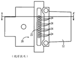
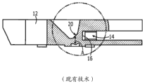
A kind of transceiver lens body 10(of example sees Fig. 1 a-1f) consistent with these light flexion technology, it comprises: body 12 has the optical fiber receiving port 14 of the interface surface 16 in this body one side; Reflecting surface 20, the light that is used for advancing along the light path A with the optical fiber approximate vertical that is arranged on port one 4 leads again; Array 22 with lens 24, described lens 24 focus between lens 24 and the interface surface 16 will be approximately perpendicular to the light that optical fiber in the port one 4 advances via reflecting surface 20 along the location, bottom 26 of body 12, for example focus on to be supported in the described port and in the optical fiber of interface surface 16.Thus, lens body 10 provides light path, and described light path is applicable to carry out optics with corresponding optical fiber in the port one 4 that is supported on lens body 10 and couple being supported on suprabasil OED.To notice such as those of ordinary skills, such lens body 10 is suitable for being included in following various cable-assembly and the transceiver, and described various cable-assemblies and transceiver can be installed in the multiple host computer system that comprises such as router, computing machine, switch (switches), bridge (bridges) and I/O card etc.
Therefore, it should be noted that aliging of described lens body and described substrate, or more specifically, described lens, light path and optical fiber and suprabasil OED to align for the correct optics between described OED and the described optical fiber couples be vital.The OED(that active (active) alignment techniques is used for that sometimes described lens body is approximately perpendicular to the base plane utilizing emitted light with respect to support or receives light is VCSEL or other light source for example) substrate align.In active alignment techniques, described light source is (luminous) that is intensified.The problem of active alignment techniques is: the method requires special imaging device, and may be expensive, particularly couples for light flexion formula optics.Also can adopt various passive (passive) alignment techniques.In a kind of passive alignment techniques, the image of light source self (for example part of VCSEL) can be via described reflecting surface and lens and is seen by human eye, has eliminated thus the needs to special imaging device.Yet, because the restriction of the tight spacing in the described OED assembly (tight spacingconstraints), so the method requires extra hardware and fixed mechanism (fixturing) with the described alignment feature of correct observation.In addition, this technology is dangerous: be identical or parallel and/or described alignment feature is described light source self (for example VCSEL) because be used for alignment and transmit the described light path of purpose, therefore and human eye is in the position that can suffer damage in the process of observing for the alignment purpose, so described light source any intensifies the infringement that will cause used human eye in the registration process process unexpectedly.In the passive alignment techniques of another kind, alignment feature is arranged on place identical with VCSEL/PIN/OED in the described substrate.Yet in such layout, the alignment structures of lens body is being parallel to and is moving apart in the Different Plane on the plane of VCSEL/PIN OED.These alignment feature are then observed to eliminate described tight spacing restriction via the path outside the described reflecting surface.Although the method is because the possibility of when the accident of light source intensifies human eye being damaged is less and safer, but because the difference of the degree of depth of the field between two planes exceeds the ability of common imaging system, the method is unsatisfactory and produce inaccurate result.Therefore, in order to realize alignment, must introduce the outside reference point, and alignment feature must snap to described reference point individually.End product is, alignment feature and alignment structures will be in alignment with each other, but the described additional step that each must be snapped to outside reference point has been introduced extra inaccuracy.
Description of drawings
In the mode of example the present invention is described referring now to the following drawings, in the accompanying drawings:
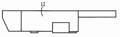
Fig. 1 a, Fig. 1 b, Fig. 1 c and Fig. 1 d are respectively vertical view, side view, upward view and the rear views of lens body of the prior art of example, and this lens body comprises: be used for making being installed on suprabasil OED and being roughly parallel to reflecting surface and the lens of the light flexion of advancing between the optical fiber of base plane;
Fig. 1 e is the sectional view of the lens body of Fig. 1 a-1d of obtaining of the line A-A ' along Fig. 1 a;
Fig. 1 f is the partial cross section figure of the lens body of Fig. 1 a-1d, and the zoomed-in view in the zone 1 of Fig. 1 e is shown;
Fig. 2 a, Fig. 2 b, Fig. 2 c and Fig. 2 d are respectively vertical view, side view, upward view and the rear views according to the lens body of example of the present invention, and the lens body of this example comprises: alignment structures and special-purpose alignment lens;
Fig. 2 e is the sectional view of the lens body of Fig. 2 a-2d of obtaining of the line B-B ' along Fig. 2 a;
Fig. 2 f is the partial cross section figure of the lens body of Fig. 2 a-2d, and the zoomed-in view in the zone 2 of Fig. 2 e is shown;
Fig. 2 g is the sectional view of the lens body of Fig. 2 a-2d of obtaining of the line C-C ' along Fig. 2 a and Fig. 2 c;
Fig. 3 is the skeleton view of the lens body of Fig. 2 a-2g, illustrates with decomposition view with respect to cranse and the substrate of example;
Fig. 4 is the part vertical view of the lens body of Fig. 2 a-2g, and the plan view of the substrate alignment feature of example is shown, and is viewed when unjustified with the alignment structures of this lens body;
Fig. 5 is the part vertical view of the lens body of Fig. 2 a-2g, and the plan view of the substrate alignment feature of example is shown, and is viewed when aliging with the alignment structures of this lens body;
Fig. 6 is the skeleton view of the lens body of Fig. 2 a-2g, and the substrate that it is installed to the example in the optical sub-assembly is shown; With
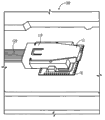
Fig. 7 is the skeleton view of the lens body of Fig. 2 a-2g, it is shown by the part of part assembling as the active cable lens subassembly of the QSFP of example.
Embodiment
Be the diagram purpose, the below discusses to the present invention with reference to lens body.As discussed above, Fig. 1 a-1f illustrates the lens body 10 of example, and this lens body 10 has the feature common with the lens body of prior art.Illustrated lens body 10 comprises: body 12, it is an example of the lens body of multiple prior art, this is that it comprises be used to being resisted against and supports for example VCSEL of one or more OED() the basal surface 26 of substrate; Port one 4 be used for to receive one or more optical fiber, and described one or more optical fiber is used for that light is carried to OED or carries light from OED; Lens 24, interface surface 16 neutralizations that are used for focusing on from the light of OED port one 4 corresponding to each OED focus on the optical fiber that is resisted against interface surface 16 (otherwise or); With reflecting surface 20, be used at OED and be resisted against the light that transmits between the optical fiber of interface surface 16 and reflect.As used herein, " against " or " interface " mean physically to contact and be against relation or almost be in physical contact, for example separated by the gap (gap) that is not more than approximate 0.025mm.Thus, lens body 10 is at suprabasil each OED and be supported between each bar optical fiber in the port one 4 light path is provided, and therefore is suitable for OED and fiber optics are coupled.
Fig. 2 a-2g illustrates the lens body 10 according to example of the present invention.This lens body can be similar in appearance to the lens body of prior art aspect its general structure, and therefore can comprise: corresponding to the active lens 24 of each OED; Optical fiber receiving port with interface surface 16; And be in the reflecting surface of the centre of the light path between the optical fiber etc. of described active lens and described port/couple.Alternatively, as known in the art, this reflecting surface can be provided as the part of total internal reflection (TIR) prism.Preferably, this lens body 10 comprises that a plurality of active lens 24(that are arranged to linear array illustrate 12), shown in Fig. 2 c and Fig. 2 d.See Fig. 2 a – 2g.Therefore, the lens body 10 of the example of Fig. 2 a-2g comprises described those the similar structures of prior art lens body to above example with reference to figure 1a-1f.In addition, the lens body 10 of Fig. 2 a-2g preferably includes: but single (unitary) body construction of optically transparent moulding material.Term " but optically transparent moulding material " is with meaning to have the little feature of loss in the transmission of optical signalling here.For example, this lens body can be formed uniformly by following method: the fluid plastic material is molded as exactly determined shape and structure so that all light path element set, for example, by carrying out injection-molded, compression molded polycarbonate (polycarbonate), polyethers-acid imide (polyether-imide) or polyethersulfone (polyethersulfone) material or transfer printing molded (transfermolding), described material for example for can by General Electric company buy such as ULTEM
TMOr RADEL
TMMaterial.Port one 4 can be configured to accept: any traditional, suitable device that cooperates with existing one or more optical fiber in cable cranse/assembly.Term " optoelectronic device " or OED are with meaning that here current transitions become light and/or light being transformed into the device of electric current.Term " light " generally refers to electromagnetic radiation, refers to that preferably semiconductor material maybe can be made into electromagnetic radiation to those wavelength of its sensitivity to its sensitivity, and no matter this light for naked eyes whether actual as seen.The example of OED comprises: laser instrument (such as Vcsel (VCSEL), double channel plane buried heterostructure type (DC-PBH), bury meniscus (BC), distributed feedback type (DFB), distributed bragg reflector mirror type (DBR) etc.), light emitting diode (LED) (for example surface-emitting type LED(SLED), edge-emission type LED(ELED), super-radiance light emitting diode SLD), Deng) and photodiode (for example PIN, avalanche photo diode (APD), etc.).As further example, OED is with being the light source of optical fiber for example here, and described optical fiber is such as being multimode (mm) optical fiber or single mode (sm) optical fiber, glass optical fiber, plastic optical fiber etc.Described OED is installed to the surface of substrate.Term " substrate " is with referring to almost any parts or article here.Yet, in the situation of optical fiber communication, term " substrate " electronic unit that refers to that here the electronic unit of electronic circuit component is installed on it or form the part of electronic circuit component.Described substrate can comprise for example a plurality of integrated chips.Such chip can represent for example prime amplifier or post amplifier and other electronic circuit.The essence of such circuit component and type, and the method and the technology that are used for such element is installed to described substrate are well known in the art and do not consist of part of the present invention.In common embodiment, described substrate comprises: chip glass (glass wafer) and/or the similar substrate well known in the art of printed circuit board (PCB) (PCB), printing distributing board (PWB), flexible print circuit (FPC), bearer circuit.
Different from the lens body of prior art, lens body 10 according to the present invention further comprises: limit the surperficial 42(of observation and see Fig. 2 a, Fig. 2 g) at least one alignment structures 40 and at least one special-purpose lens 50(see Fig. 2 c, Fig. 2 g), described at least one special-purpose lens 50 are positioned at outside any light path between the optics, that pass lens body 10.Preferably, described lens body comprises at least one pair of special-purpose lens 50.Alternatively, described a pair of special-purpose lens 50 are arranged in the identical single linear array in company with active lens 24, illustrate such as Fig. 2 c the best.In such embodiments, all a plurality of active lenses 24 can be positioned in linear array between the described a pair of special-purpose lens 50, shown in Fig. 2 c.Described special-purpose lens can help correct alignment with respect to this location of described active lens.
In a preferred embodiment, alignment structures 40 is adjoined general plane type observation surface 42 and is limited hole (void) 46 in body 12, illustrate such as Fig. 2 g the best.As example, described hole can be formed by centrepin (core pin) in the injection-molded process of described body, so that press polished observation surface 42 to be provided, to help to observe projection image thereon.In the example embodiment shown in Fig. 2 a-2g, alignment structures 40 forms so that hole 46 has down frusto-conical.Although can adopt any suitable structure, this shape has advantage aspect body 12 molded, and has additional advantage: it provides the observation surface 42 with circular, circumferential border 48, shown in Fig. 4 the best.Such border can the image 44 of alignment structures 74 centers when differentiating/and favourable to the people when observing surface 42 and align, as will be discussed.Yet any suitable shape and structure can be used for described alignment structures and/or described observation surface/border.
In addition, substrate 70 is according to the present invention and special tectonic, to comprise at least one appreciable alignment feature 74.As example, the alignment feature of described substrate can be configured to present lip-deep for example circle, plus sige, X or any other the appreciable image that is printed on or is arranged on substrate 70 with other different modes.As example, described alignment feature the metallic film that provides by accurate chemical etching processing is provided is arranged in the substrate 70.Preferably, alignment feature 74 is generally flat, and places the plane roughly the same with the light-emitting area of described light source.This makes the alignment lens of described special use can have the shape identical with active lens and can utilize identical instrument/processing and make, eliminate thus mould (mold) and make the change (change-over) of processing unit (plant), described change may be introduced error at described special-purpose lens aspect the position of active lens.In one embodiment, such single alignment feature is set, this single alignment feature can cooperate with the alignment feature of another kind of form, and for example mechanical type pin-jack is arranged.In a preferred embodiment, in described substrate at least one pair of such alignment feature is set.
The alignment feature of substrate is arranged to be predetermined spatial relationship with respect to the OED in the substrate 70.This predetermined spatial relationship is corresponding to special-purpose lens 50 and the spatial relationship of observing between surperficial 42 in lens body 10.In this way, the alignment feature 74 of substrate will be guaranteed with the aliging of observation surface 42 of lens body: correctly the aliging of the optical fiber that active lens 24, the light path of OED80 and lens body and being connected is connected.Each special-purpose lens 50 is applicable to the alignment feature 74(of substrate is seen Fig. 3) image 44(see Fig. 4 and Fig. 5) focus on and observe on the surface 42, to be used for that lens body 10 is seen Fig. 3 with substrate 70() correct purpose of aliging, or more specifically, be applicable to active lens 24, light path and optical fiber are alignd with OED80 in the substrate 70, couple with the correct optics that is used between described OED and the described optical fiber.
In a preferred embodiment, active lens 24 and special-purpose lens 50 are constructed with roughly the same optical specification (prescription), so that they have roughly the same focal length.In such embodiments, each is observed surface 42 and is positioned on the lens body 10, so that the optical path length between active lens 24 and the interface surface 16 (X+Y, Fig. 2 f) is substantially equal to the optical path length (Z, Fig. 2 g) between special-purpose lens 50 and the observation surface 24.In this embodiment, the image 44 of the alignment feature 74 of substrate and observe surface 24 both are arranged in same (or almost same) plane, and because both will in the field of observation point same depth, clearly present, so both can be by human eye or traditional imaging system easily and clearly perception.This so that do not need to focus on and the Different Plane of disposing different depth of field of aliging in different alignment feature, and help accurate alignment, even only use human eye.
In alternate embodiment, described special-purpose lens have the specification/focal length that is different from active lens.In such embodiments, the optical path length between active lens and the interface surface will preferably not be the optical path length that is substantially equal between described special-purpose lens and the observation surface.As an alternative, the optical path length between described special-purpose lens and the observation surface is substantially equal to the focal length of described special-purpose lens.
In the preferred embodiment of lens body 10, for example shown in Fig. 2 a-2g, lens body 10 further comprises: at least one reflecting surface 20 that between OED80/ active lens 24 and interface surface 16/ optical fiber, along one or more light paths, arranges, and in order to change the direction of the light path between each OED and its corresponding optical fiber.The light path that each special-purpose lens 50 and each be corresponding observes between the surface 42 is preferably linear.Thus, in such embodiments, the light path of observing between surface 42 and the special-purpose lens 50 is not passed reflecting surface 20.In addition, observe the light path of light path preferred parallel between active lens 24 and reflecting surface 20 between surface 42 and the special-purpose lens 50, and/or perpendicular to the light path between reflecting surface 20 and the interface surface 16, and/or perpendicular to the optical axis of any optical fiber in the cranse that is positioned in the port one 4.
The lens body 10 of Fig. 2 a-2g can be used for preparing the optical sub-assembly that comprises this lens body.The method for preparing such optical sub-assembly comprises the substrate 70(Fig. 3 that provides support OED80), described OED80 for example is light source.Such substrate can be traditional type roughly in itself, for example with the thin chip glass of order wire circuit, therefore is used for providing the technology of described substrate not discuss in further detail at this.Yet this step further comprises provides substrate, and this substrate comprises at least one the appreciable alignment feature 74(Fig. 3 that is arranged to be for described light source predetermined spatial relationship).Preferably, described substrate comprises at least one pair of alignment feature, and described each alignment feature is with people's naked eyes visual perception.Be used for providing such as circle ,+or the technology of the alignment feature such as X comprise that accurate chemical etching processes.Perhaps, described alignment feature is appreciable, but can not utilize the naked eyes visually-perceptible.For example, such alignment feature can comprise VCSEL or other light source that infrared target for example is fit to, and the imaging device that is fit to is used for the described alignment feature of perception to be used for the alignment purpose.
Described method further comprises: lens body 10 is provided, and body 12 is positioned in the substrate 70, so that the alignment feature 74 of substrate can be observed on the observation surface 42 of the alignment structures 40 of lens body, illustrate such as Fig. 4 the best.Described method further comprises: move body 12 with respect to substrate 70, until the image 44 of the alignment feature 74 of substrate is rendered as alignment with respect to observing surface 42 and/or its peripheral boundaries 44, for example centering illustrates such as Fig. 5 the best.For comprising more than an alignment feature with more than the lens body of an alignment structures, this lens body should be moved until all images 44 is rendered as alignment simultaneously with respect to the corresponding surface of observing.Then lens body 12 should be fixed with respect to described substrate.As known in the art, this step may relate to and applies and solidify suitable epoxy, for example curable epoxy of UV.
Therefore, optical sub-assembly 100 is provided as and comprises: the substrate 70 with at least one appreciable alignment feature 74, with the lens body that is fixed to described substrate, so that lens body 10 and substrate 70 are fixed in the relative position, in described relative position each alignment feature 74 of substrate 70 the alignment feature 40 of lens body corresponding observe be rendered as centering in the surface 42 or otherwise be rendered as alignment, illustrate such as Fig. 5 and Fig. 6 the best.In addition, optical sub-assembly 100 can comprise: support the cranse of at least one optical fiber 120, for example many optical fiber cranse 110 or other attachment unit interface illustrate such as Fig. 3 and Fig. 6 the best.Fig. 7 illustrates optical sub-assembly 100, and this optical sub-assembly 100 is depicted as and is installed to conventional housings as the part of the active cable-assembly 200 of the QSFP of example.Should be understood that optical sub-assembly 100 can utilize exceeds the scope of the invention and is assembled into any suitable cable-assembly for example in the active cable-assembly of CXP at the traditional group packing technique that this does not have to describe in detail, and is assembled in the transceiver module of any correspondence.
The light path that should be understood that lens body 16 and wherein limit only is representative of the present invention, and non exhaustive.
More than having described special-purpose lens/alignment feature/alignment structures for the purpose of giving an example with reference to lens body arranges.Yet, it should be noted that this layout can be alignment and the purpose of interposed structure and is applicable to the application of broad range.For example, described layout can be used in the application that any wherein two objects will relative to each other align.In addition, described layout can be used for other situation except optical application.For example, similar layout is used in and carries out in the past aligned surfaces installing component of Reflow Soldering (solder reflow) in the printed circuit board (PCB).