CN102999453A - Universal nonvolatile memory control device for system on chip - Google Patents
Universal nonvolatile memory control device for system on chip Download PDFInfo
- Publication number
- CN102999453A CN102999453A CN2012103866844A CN201210386684A CN102999453A CN 102999453 A CN102999453 A CN 102999453A CN 2012103866844 A CN2012103866844 A CN 2012103866844A CN 201210386684 A CN201210386684 A CN 201210386684A CN 102999453 A CN102999453 A CN 102999453A
- Authority
- CN
- China
- Prior art keywords
- write
- register
- data
- control
- interface unit
- Prior art date
- Legal status (The legal status is an assumption and is not a legal conclusion. Google has not performed a legal analysis and makes no representation as to the accuracy of the status listed.)
- Granted
Links
- 230000015654 memory Effects 0.000 title claims abstract description 112
- 238000004088 simulation Methods 0.000 claims description 46
- 230000007704 transition Effects 0.000 claims description 13
- 238000000034 method Methods 0.000 claims description 12
- 230000008569 process Effects 0.000 claims description 12
- 230000008676 import Effects 0.000 claims description 3
- 238000006243 chemical reaction Methods 0.000 abstract description 10
- 238000012938 design process Methods 0.000 abstract description 4
- 238000012545 processing Methods 0.000 abstract description 3
- 230000006870 function Effects 0.000 description 12
- 238000011084 recovery Methods 0.000 description 8
- 238000002679 ablation Methods 0.000 description 4
- 238000013461 design Methods 0.000 description 4
- 230000001413 cellular effect Effects 0.000 description 3
- 238000010276 construction Methods 0.000 description 3
- 238000005498 polishing Methods 0.000 description 3
- 102100037620 Centrin-1 Human genes 0.000 description 2
- 101000880499 Homo sapiens Centrin-1 Proteins 0.000 description 2
- 230000008859 change Effects 0.000 description 2
- 241001269238 Data Species 0.000 description 1
- 230000009286 beneficial effect Effects 0.000 description 1
- 230000007812 deficiency Effects 0.000 description 1
- 238000005516 engineering process Methods 0.000 description 1
- 239000012467 final product Substances 0.000 description 1
- 238000004519 manufacturing process Methods 0.000 description 1
- 239000000463 material Substances 0.000 description 1
- 239000000047 product Substances 0.000 description 1
- 238000012360 testing method Methods 0.000 description 1
Images


Landscapes
- Read Only Memory (AREA)
Abstract
The invention relates to a universal nonvolatile memory control device for a system on a chip. The control device comprises an external bus interface unit, a register control unit, an erasing unit and a storage control and interface unit. The external bus interface unit is used for collecting control signals and data of an external bus as well as analyzing the signals and data; the register control unit is used for read-write control of all registers, wherein the register data is transmitted to the storage control and interface unit for use by a finite-state machine of the storage control and interface unit; the erasing unit is used for processing bus signals transmitted by the external bus interface unit; the storage control and interface unit comprises two finite-state machines: one is a write data width conversion state machine, while the other is a master control state machine for read, write and erase control of various nonvolatile memories. The invention provides the universal nonvolatile memory control device for the system on the chip good in compatibility and simplified in design process.
Description
Technical field
The present invention relates to belong to System on Chip/SoC (SoC) Integrated design field, what be specifically related to a kind of highly compatible is used for the integrated general control device of non-volatile storage of System on Chip/SoC.
Background technology
Along with improving constantly of integrated circuit manufacture level, the complication system that the deviser is can be on single-chip integrated millions of, i.e. SOC (system on a chip) (System-On-Chip).In recent years, SoC has become the main flow direction of current integrated circuit (IC) design, in order to satisfy the demand of more and more diversified various practical applications, as the important devices of storage data, polytype nonvolatile memory (Non-Volatile-Memory) also progressively is being integrated into the SoC chip internal.These nonvolatile memories comprise OTP, EEPROM, FLASH etc.
Dissimilar nonvolatile memories has different control signals and sequential requirement usually, therefore, for different nonvolatile memories, often needs to design different Memory Controllers, to satisfy the control to the particular type nonvolatile memory.Simultaneously, in order to reach the purpose to this non-volatile memory controller real simulation, also need additional designs very targetedly emulation controller realize emulation.
In a lot of situations, almost completely identical with the most of assembly of a series of SoC chip, perhaps only be that the capacity of nonvolatile memory wherein or type are different, but need to redesign the different Memory Controller of exploitation and corresponding emulation controller meets the demands.In this process, namely spend a large amount of human and material resources and time, also incured loss through delay the popularization of SoC chip product and the time of software development simultaneously.
Summary of the invention
In order to overcome compatible relatively poor, the deficiency that design process is complicated of existing nonvolatile memory, the invention provides that a kind of compatibility is good, design processes simplified for the integrated general control device of non-volatile storage of System on Chip/SoC.
The technical solution adopted for the present invention to solve the technical problems is:
A kind of for the integrated general control device of non-volatile storage of System on Chip/SoC, described control device comprises external bus interface unit, register control module, erasable unit and storage control and interface unit, wherein,
The external bus interface unit is used for gathering control signal and the data of external bus, and analyzes: if access control register imports bus signals into the register control module; If non-volatile memory cells is carried out read operation, bus signals is passed to storage control and interface unit, realize the read operation to non-volatile memory cells; If non-volatile memory cells is carried out write operation, bus signals is passed to erasable unit;
The register control module, be used for all registers are read and write control, described all registers comprise OTP mode of operation register, EFLASH mode of operation register, EEPROM mode of operation register, OTP sequence control register, EFLASH sequence control register, EEPROM sequence control register and virtual timing simulation register, register data will be passed to storage control and interface unit, for the finite state machine of storage control with interface unit;
Erasable unit, the bus signals that transmits for the treatment of the external bus interface unit;
Storage control comprises two finite state machines with interface unit; One is to write data width transition status machine, be used for when data width that data width and the virtual nonvolatile memory of nonvolatile memory are simulated is 16 or 8, according to the byte effective information of erasable unit output 32 of erasable unit output being write Data Division is a plurality of 16 or 8 bit data, and passes to successively nonvolatile memory by the control of major state machine;
Another is the major state machine, be used for polytype, several data width nonvolatile memory are carried out reading and writing, wipe control, described type is EFLASH, OTP and EEPROM, described data width is 8,16,32 and 64, also support 32 SRAM of byte-accessed that true reading and writing, the wiping sequential of polytype, several data width nonvolatile memory are simulated by 2 simultaneously, become virtual non-volatile memory controller.
Further, in the described erasable unit, when carrying out normal total line write transactions, erasable unit with the write address in the bus signals, write data, data size information intercepts out and process, produce address in the corresponding page or leaf of this total line write transactions, byte effective information (only when data width use when being 16 or 8) and this page write operation (during EEPROM page or leaf write operation, once page or leaf can be carried out repeatedly total line write transactions in the write operation) page address, simultaneously this page write or continuously the data total amount information of write operation add up; These information are temporarily stored in FIFO and the register together with the data of writing of each total line write transactions, export to storage control and interface unit when the finite state machine in storage control and the interface unit needs.
Further, in the described register control module, described all registers also comprise status register, are used for reflecting the duty of current control store control and interface unit major state machine.
Described virtual timing simulation register comprise read the timing simulation register, write the timing simulation register, page or leaf is wiped the timing simulation register and full sheet is wiped the timing simulation register, when as virtual non-volatile memory controller, can be used for the analog nonvolatile storer read latch, write time-delay, page or leaf and wipe time-delay and full sheet and wipe and delay time.
Technical conceive of the present invention is: pass through hardware configuration, reading and writing, wiping control to multiple nonvolatile memory both can have been supported, also can be by the simulation of SRAM realization to the true reading and writing of multiple nonvolatile memory, wiping sequential, become virtual non-volatile memory controller, be used for the emulation of objective chip and the assessment of test chip.Specific features is as follows:
1) supports 32 ahb bus interfaces, multiple nonvolatile memory can be connected on the ahb bus when System on Chip/SoC is integrated, thereby multiple nonvolatile memory is conducted interviews and control by external bus.By hardware configuration, the types of non-volatile of support comprises OTP, EFLASH and EEPROM.
2) when control OTP, support to read and write continuously function, so-called writing continuously refers to can write a plurality of data in the write operation of an OTP.
3) when control EFLASH, support is read, forms data is write, page or leaf is wiped and full sheet is wiped function, so-called forms data is write and refer to write data in the write operation of an EFLASH, so-called page or leaf is wiped and is referred to that disposable one page wiping with EFLASH is complete " 1 ", and so-called full sheet wiping refers to that disposable full sheet EFLASH is wiped is complete " 1 ".
4) when control EEPROM, support is read, page or leaf is write and full sheet is wiped function.So-called page or leaf is write a plurality of data that refer to can write with in one page in the write operation of an EEPROM, so-called full sheet is wiped and referred to that disposable full sheet EEPROM is wiped is complete " 1 ".
5) by hardware configuration, support the nonvolatile memory of several data width, comprise 8,16,32 and 64.
6) pass through hardware configuration, except supporting reading and writing, the wiping control to multiple nonvolatile memory, can also support 32 SRAM of byte-accessed to realize the simulation of polytype, the true reading and writing of several data width nonvolatile memory, wiping sequential is become virtual non-volatile memory controller by two.When as virtual non-volatile memory controller, can be according to the control of external data width pin, need not to change SRAM and just can realize simulation to the nonvolatile memory of 8,16,32 and 64 bit data width.
7) word of supporting bus, half-word, byte manipulation when the memory data width is 8; The word of supporting bus, half word operation when the memory data width is 16; The word operation of supporting bus when the memory data width is 16; The word read operation of supporting bus when the memory data width is 64, this moment, total line write transactions required take a double word as the unit data writing (because external bus is 32 bit widths, so require to write two words in the double word by twice total line write transactions);
8) unify the programming mode of external bus to dissimilar nonvolatile memories, be convenient to the user software exploitation.No matter be as OTP, EEPROM, EFLASH controller, or virtual non-volatile memory controller, external bus was reduced to for three steps to the write operation unification of nonvolatile memory: normal total line write transactions (if OTP or EEPROM, then can be in write operation writing a plurality of data by total line write transactions repeatedly) is carried out in the address that at first needs is write; The configuration effort mode register is initiated write request again; Inquire about at last the status register in the register control module until state is idle.
Beneficial effect of the present invention is mainly manifested in: compatible good, design processes simplified.
Description of drawings
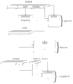
Fig. 1 is the nonvolatile memory controller architecture.
Fig. 2 is erasable cellular construction (the memory data width is 64).
Fig. 3 is erasable cellular construction (the memory data width is 32).
Fig. 4 is erasable cellular construction (the memory data width is 16 or 8).
Fig. 5 is virtual non-volatile memory controller SRAM structure (the simulated data width is 64).
Fig. 6 is virtual non-volatile memory controller SRAM structure (the simulated data width is 16 or 8).
Fig. 7 writes data width transition status machine.
Fig. 8 is the major state machine.
Fig. 9 is major state machine state conversion (during control OTP).
Figure 10 is major state machine state conversion (during control EEPROM).
Figure 11 is major state machine state conversion (during control EFLASH).
Figure 12 is major state machine state conversion (as virtual non-volatile memory controller time).
Embodiment
The invention will be further described below in conjunction with accompanying drawing.
With reference to Fig. 1 ~ Figure 12, a kind of for the integrated general control device of non-volatile storage of System on Chip/SoC, comprise external bus interface unit, register control module, erasable unit and storage control and interface unit.By the collaborative work of these unit, realize to the compatible of multiple nonvolatile memory and to the simulation of multiple nonvolatile memory:
Control signal and the data of external bus are responsible for gathering in the external bus interface unit, and analyze: if access control register imports bus signals into the register control module; If non-volatile memory cells is carried out read operation, bus signals is passed to storage control and interface unit, realize the read operation to non-volatile memory cells; If non-volatile memory cells is carried out write operation, bus signals is passed to erasable unit.
The register control module is responsible for all registers of this non-volatile memory controller are read and write control, comprise OTP mode of operation register, EFLASH mode of operation register, EEPROM mode of operation register, the OTP sequence control register, the EFLASH sequence control register, the EEPROM sequence control register, virtual timing simulation register (comprises and reads the timing simulation register, write the timing simulation register, page or leaf wipes the timing simulation register and full sheet is wiped the timing simulation register, the read latch that is used for the analog nonvolatile storer, write time-delay, page or leaf is wiped time-delay, full sheet is wiped time-delay) etc., these register datas will be passed to storage control and interface unit, for the finite state machine of storage control with interface unit.In addition, also comprise status register, be used for reflecting the duty of current control store control and interface unit major state machine.
Erasable unit is responsible for processing the external bus interface unit and is transmitted bus signals.When carrying out normal total line write transactions, erasable unit with the write address in the bus signals, write data, data size information intercepts out and process, produce address in the corresponding page or leaf of this total line write transactions, byte effective information (only when data width use when being 16 or 8) and this page write operation (during EEPROM page or leaf write operation, once page or leaf can be carried out repeatedly total line write transactions in the write operation) page address, simultaneously this page write or continuously the data total amount information of write operation add up; These information are temporarily stored in FIFO and the register together with the data of writing of each total line write transactions, export to storage control and interface unit when the finite state machine in storage control and the interface unit needs.Owing to used FIFO, the user can carry out repeatedly total line write transactions in the write operation of a nonvolatile memory, thereby with a plurality of write addresses, write data and write the byte effective information and deposit in successively among the FIFO, with the page or leaf write operation of supporting EEPROM and the continuous write operation of OTP.
Storage control comprises two finite state machines with interface unit:
One is to write data width transition status machine, its major function is: when the data width of the data width of nonvolatile memory and the simulation of virtual nonvolatile memory is 16 or 8, according to the byte effective information of erasable unit output 32 of erasable unit output being write Data Division is a plurality of 16 or 8 bit data, and passes to successively nonvolatile memory by the control of major state machine.
Another is the major state machine, be responsible for multiple nonvolatile memory is carried out reading and writing, wipes control, and realize by 2 support 32 SRAM of byte-accessed to the true reading and writing of multiple nonvolatile memory, wipe sequential and simulate.
Described in summary of the invention, this non-volatile memory controller is reduced to three steps with external bus to the write operation unification of nonvolatile memory, and this function is mainly realized by erasable unit.Such as Fig. 2, Fig. 3, shown in Figure 4, erasable unit is responsible for processing the external bus interface unit and is transmitted bus signals.Its principle of work is as follows:
1) when carrying out 1 of nonvolatile memory write operation step, when namely carrying out normal total line write transactions, erasable unit with the write address in the bus signals, write the intercepting of data and data size information (byte, half-word or word) out and process, be temporarily stored in FIFO and the register.
2) register of indication comprises page address register and writing data quantity counter 1).The former records the page address of this nonvolatile memory write operation (because OTP does not have the concept of page or leaf according to the write address of for the first time total line write transactions in this nonvolatile memory write operation, so do not have this register during control OTP, the address all is recorded among the FIFO of address); The latter records the data volume among the FIFO, and digit is the data width of current storage or the data width of virtual nonvolatile memory simulation.
3) FIFO of indication comprises data FIFO, address FIFO and the effective FIFO of byte 1), major function is: the page or leaf of the writing continuously of OTP, EEPROM write and the corresponding simulated operation realized by SRAM in, the user can carry out repeatedly total line write transactions in the write operation of a nonvolatile memory, thereby with addresses in a plurality of pages or leaves, write data and write byte effective information (when the memory data width is 16 or 8, using) and deposit among the FIFO successively.
4) width of data FIFO is 32, and the width of the effective FIFO of byte is 4 (respectively 4 bytes of corresponding 32 bit data).When carrying out the EEPROM write operation, because a write operation can be write one page at most, so the degree of depth of the width of address FIFO and each FIFO can be according to the page or leaf size configure of nonvolatile memory; When carrying out the EFLASH write operation, owing to once can only write data, so the degree of depth of FIFO is 1 at this moment, the width of address FIFO is according to EFLASH page or leaf size configure; When carrying out the continuous write operation of OTP, owing to there is not the concept of page or leaf, so the degree of depth of each FIFO does not limit at this moment, can define according to user's request, the width of address FIFO is according to the size configure of otp memory, and write address all is recorded among the FIFO of address.
5) when carrying out 2 of nonvolatile memory write operation step, when namely the configuration effort mode register was initiated write request, the finite state machine in storage control and the interface unit started.When finite state machine is carried out corresponding state, erasable unit with address in the page or leaf, write data, the byte effective information is write fashionable order according to bus and is taken out successively, passes to storage control and interface unit together with information such as page address, data total amounts.
6) when carrying out 3 of nonvolatile memory write operation step, i.e. query State register is until the finite state machine end of run in storage control and the interface unit.
In order to support writing of several data width, comprise 64,32,16 and 8, the FIFO of erasable unit can realize different structures by hardware configuration:
1) when the data width of nonvolatile memory is 64, as shown in Figure 2, erasable unit comprises 32 bit data FIFO and address FIFO of two parallel connections, require this moment external bus take a double word as the unit data writing (because external bus is 32 bit widths, so require to write two words in the double word by twice total line write transactions), 32 bit data FIFO of two parallel connections can deposit respectively the data in total line write transactions in this twice, be two words in the double word, simultaneously address FIFO intercepts in this twice total line write transactions once, obtain and deposit in address in page or leaf corresponding to this double word (because 64 alignment, so 2 to 0 omit).64 being write data and write address (comprising address in page address and the page or leaf) when the storage control finite state machine with interface unit in needs writes fashionable order according to bus and passes to successively to store and control and interface unit.
2) when the data width of nonvolatile memory is 32, as shown in Figure 3, erasable unit comprises 32 bit data FIFO and an address FIFO, when the external bus data writing, can will write data with write address deposits respectively data FIFO and address FIFO in, when the finite state machine of storage control with interface unit in needs, 32 write data and write address (comprising address in page address and the page or leaf) and write fashionable order according to bus and pass to successively to store and control and interface unit.
3) when the data width of nonvolatile memory is 16 or 8, as shown in Figure 4, erasable unit comprises 32 bit data FIFO, an address FIFO and the effective FIFO of 4 bit bytes, when the external bus data writing, meeting will write data and write address deposits respectively data FIFO and address FIFO in, (data size information of ahb bus is hsize to low sum-bit data size information by overall treatment bus write address simultaneously, reflected that current total line write transactions is byte, half-word or word), obtain these 32 and write the corresponding byte effective information of data, deposit the effective FIFO of byte in, when the finite state machine in storage control and the interface unit needs, write data with 32, write address (comprising page address address in page or leaf) and byte effective information are write fashionable order according to bus and are passed to successively storage control and interface unit.
4) when as virtual non-volatile memory controller, erasable unit comprises two 32 bit data FIFO, an address FIFO and the effective FIFO of 4 bit bytes.Can realize 1 according to the control of external data width pin this moment), 2) or 3) in structure, thereby realize simulation to 8,16,32 and 64 bit data width.
When this non-volatile memory controller becomes virtual non-volatile memory controller by hardware configuration, storage control not only comprises with interface unit writes data width transition status machine and major state machine, also comprises the steering logic of supporting 32 SRAM of byte-accessed to two.This moment is by external data width pin control, can realize the simulation to 8,16,32 and 64 bit data width, need not to change SRAM, and concrete mode is as follows,
1) when external data width pin represents 64, such as Fig. 5, the chip selection signal CEN0 of these two SRAM and CEN1 homology, (write address is from erasable unit through 64 registration process for reference address, read the address from the external bus interface unit), this moment, two SRAM became relation in parallel, were equivalent to the SRAM of 64 of whole pieces, thereby realized the simulation to 64 bit non-volatile storeies.
2) when external data width pin represents 32,16 or 8, such as Fig. 6, (write address is from erasable unit through 32 registration process for reference address, read the address from the external bus interface unit), and the chip selection signal CEN0 of these two SRAM and CEN1 are by the most significant digit control of reference address.When access first half space, namely the most significant digit of reference address is 0 o'clock, access SRAM1, otherwise access SRAM2, and this moment, two SRAM became series relationship, were equivalent to the SRAM of 32 of whole pieces, thereby realized the simulation to 32 bit non-volatile storeies.Write enable signal WEN owing to support 32 SRAM of byte-accessed to comprise 4,4 bytes of corresponding 32 bit data of difference, therefore when 16 of simulations or 8 bit data width, although be input as 32 bit data, but control respectively these 4 by 4 bit byte effective informations of the effective FIFO output of byte in the erasable unit and write enable signal, as shown in Figure 6,32 SRAM is write in 16 or 8 s' mode, thereby realize the simulation to 16 or 8 bit non-volatile storeies.
Writing data width transition status owner and will be used for writing the conversion of data width in storage control and the interface unit.When the data width of nonvolatile memory is 16 or 8, it is a plurality of 16 or 8 bit data that this state machine is write Data Division according to the byte effective information of erasable unit output with 32 of erasable unit output, and passes to successively nonvolatile memory by the control of major state machine.(when as 16 of virtual non-volatile memory controller simulations or 8 bit data width, such as Fig. 6, because SRAM and data FIFO all are 32, do not need work so write data width transition status machine this moment, control respectively these 4 with 4 bit byte effective informations of the effective FIFO of byte in erasable unit output and write enable signal, can realize the simulation to 16 or 8 bit memory write operations)
Concrete state is changed as shown in Figure 7:
IDLE: during without write operation, state machine is defaulted as the IDLE state.When data and write address were write in the request of major state machine, if the memory data width is 16, state machine entered the 16_POP1 state; If the memory data width is 16, state machine enters the 8_POP1 state.
16_POP1: eject (POP) 32 and write data this moment from data FIFO, ejects a write address from the FIFO of address, ejects one 4 byte effective information from the effective FIFO of byte.And judge that according to the byte effective information this time corresponding total line write transactions is that word or half-word write:
If word writes, namely four bytes are all effective, so first the first two byte (16) and corresponding write address passed to the major state machine.When the major state machine was initiated write data requests again, state machine entered the 16_W_POP2 state.
If half-word writes, namely only have two bytes effective, so these two bytes and corresponding write address are passed to the major state machine.When the major state machine asked to write data again, state machine reentered the 16_POP1 state; If the write operation of major state machine all finishes, then return the IDLE state.
16_W_POP2: pass to major state machine with latter two byte in four effective bytes and corresponding write address this moment.When the major state machine was initiated write data requests again, state machine reentered the 16_POP1 state; If the write operation of major state machine all finishes, then return the IDLE state.
8_POP1: eject (POP) 32 and write data this moment from data FIFO, ejects a write address from the FIFO of address, ejects one 4 byte effective information from the effective FIFO of byte.And judge that according to the byte effective information this time corresponding total line write transactions is that word, half-word or byte write:
If word writes, namely four bytes are all effective, so first first byte and corresponding write address passed to the major state machine.When the major state machine was initiated write data requests again, state machine entered the 8_W_POP2 state.
If half-word writes, namely two bytes are effective, so first first byte in these two bytes and corresponding write address passed to the major state machine.When the major state machine was initiated write data requests again, state machine entered the 8_HW_POP2 state.
If byte writes, namely only have a byte effective, so this byte and corresponding write address are passed to the major state machine.When the major state machine asked to write data again, state machine reentered the 8_POP1 state; If the write operation of major state machine all finishes, then return the IDLE state.
8_W_POP2: pass to major state machine with second byte and corresponding write address in four effective bytes this moment.When the major state machine was initiated write data requests again, state machine entered the 8_W_POP3 state.
8_W_POP3: pass to major state machine with the 3rd byte and corresponding write address in four effective bytes this moment.When the major state machine was initiated write data requests again, state machine entered the 8_W_POP4 state.
8_W_POP4: this moment, just the 4th byte and the corresponding write address in four effective bytes passed to the major state machine.When the major state machine was initiated write data requests again, state machine reentered the 8_POP1 state; If the write operation of major state machine all finishes, then return the IDLE state.
8_HW_POP2: pass to major state machine with second byte and corresponding write address in two effective bytes this moment.When the major state machine was initiated write data requests again, state machine reentered the 8_POP1 state; If the write operation of major state machine all finishes, then return the IDLE state.
Since more than write the existence of data width transition status machine, realized the support to several data width write operation, and in order to support the read operation to the several data width, this part function mainly realizes by storage control and major state machine and buffer register in the interface unit:
1) if the memory data width is 64, i.e. 64 bit data are read in a read operation, and then wherein 32 bit data of bus requirements reply to external bus, and this 64 bit data and address thereof are temporarily stored in the buffer register of storing in control and the interface unit.When read memory again, judge whether the address in reading address and the buffer register is same double word, if so, then directly from buffer register, read 32 bit data that need, to improve access speed.
2) if the memory data width is 32, i.e. 32 bit data are read in a read operation, directly this 32 bit data are replied to external bus when then the READ state finishes.
3) if the memory data width is 16,16 bit data are read in an i.e. read operation, then the major state machine is judged the data size information of bus: if read half-word, after then carrying out a read operation this 16 bit data polishing is replied to external bus (when for virtual nonvolatile memory, because SRAM reality still is 32, gets final product so directly this 32 bit data is replied to external bus); If read full word, then the major state machine is carried out twice read operation continuously to storer, 32 bit data that read are replied to external bus (when for virtual nonvolatile memory, for the real simulation read operation, also carry out continuously twice read operation, 32 bit data that will read at last reply to external bus).
4) if the memory data width is 8,8 bit data are read in an i.e. read operation, then the major state machine is judged the data size information of bus: if read byte, after then carrying out a read operation this 8 bit data polishing is replied to external bus (when for virtual nonvolatile memory, because SRAM reality still is 32, so directly this 32 bit data is replied to external bus); If read half-word, then carry out continuously twice read operation, the 16 bit data polishings that read are replied to external bus (when for virtual nonvolatile memory, for the real simulation read operation, also carry out continuously twice read operation, 32 bit data that will read at last reply to external bus); If read full word, then the major state machine is carried out four read operations continuously to storer, 32 bit data that read are replied to external bus (when for virtual nonvolatile memory, for the real simulation read operation, also carry out continuously four read operations, 32 bit data that will read at last reply to external bus).
The major state facility of storing in control and the interface unit have higher compatibility, are used for realizing to the control of multiple nonvolatile memory and by SRAM the read-write wiping sequential of multiple nonvolatile memory being simulated.The structure of major state machine as shown in Figure 8, the below is elaborated according to different configurations.
1) when control OTP, function is read and is write continuously in the support of major state machine, and this moment, the state conversion was shown in Fig. 9:
IDLE: during without any operation, state machine is defaulted as the IDLE state.This moment OTP chip selection signal PCEB, write enable signal PWEB and output enable signal POEB is invalid, mode signal PTM[2:0] be standby mode.When the user is WriteMode by external bus with the OTP mode of operation register configuration in the register control module, the write operation of OTP is begun, state machine enters the WEPRE state; When external bus is initiated read request by the external bus interface unit, the read operation of OTP is begun, state machine enters the RPRE state.
WEPRE: this moment is with write address and write data (if data width is 64 or 32, by address FIFO and data FIFO output; If be 16 or 8, by the output of write address transition status machine) pass to OTP, and the chip selection signal PCEB of OTP is set to effectively.According to the time-delay (sequential according to OTP requires configuration) of the OTP sequence control register defined in the register control module, behind the certain hour, state machine enters " CMOD " state.
CMOD: the chip selection signal PCEB that keeps OTP this moment is for effectively, and with the mode signal PTM[2:0 of OTP] be set to programming mode.According to the time-delay (sequential according to OTP requires configuration) of the OTP sequence control register defined in the register control module, behind the certain hour, state machine enters " WE " state.
WE: keep the chip selection signal PCEB of OTP this moment for effectively, keep the mode signal PTM[2:0 of OTP] be programming mode, and the enable signal PWEB that writes of OTP is set to effectively.According to the time-delay (sequential according to OTP requires configuration) of the OTP sequence control register defined in the register control module, behind the certain hour, state machine enters " WD " state.
WD: the chip selection signal PCEB that keeps OTP this moment keeps the mode signal PTM[2:0 of OTP for effectively] be programming mode, and with OTP write enable signal PWEB be set to invalid.Judge among FIFO this moment whether also have data according to the writing data quantity counter in the erasable unit simultaneously,, then enter " WES " state if do not have, otherwise, the ablation process that " NW " state begins next data entered.
NW: begin the ablation process of next data this moment, keep the chip selection signal PCEB of OTP for effective, it is invalid keeping and writing enable signal PWEB, keep the mode signal PTM[2:0 of OTP] be programming mode, and with next write address with write data (if be 64 or 32, then by the output of address FIFO and data FIFO; If be 16 or 8, then by write address transition status machine output) pass to OTP.According to the time-delay (sequential according to OTP requires configuration) of the OTP sequence control register defined in the register control module, behind the certain hour, state machine enters " WE " state again.
WES: keep the chip selection signal PCEB of OTP this moment for effective, it is invalid keeping and writing enable signal PWEB, keeps the mode signal PTM[2:0 of OTP] be programming mode.According to the time-delay (sequential according to OTP requires configuration) of the OTP sequence control register defined in the register control module, behind the certain hour, state machine enters " CD " state.
CD: keep the mode signal PTM[2:0 of OTP this moment] be programming mode, keep OTP write enable signal PWEB be set to invalid, and the chip selection signal PCEB of OTP is set to invalid.According to the time-delay (sequential according to OTP requires configuration) of the OTP sequence control register defined in the register control module, behind the certain hour, state machine enters " WAIT " state.
WAIT: keep the chip selection signal PCEB of OTP and to write enable signal PWEB be invalid, and with the mode signal PTM[2:0 of OTP] again put back standby mode, this moment, OTP entered the reparation state (Program Recovery) of programming.According to the time-delay (sequential according to OTP requires configuration) of the OTP sequence control register defined in the register control module, behind the certain hour, state machine returns " IDLE " state, and write operation is finished.
RPRE: this moment, chip selection signal PCEB and the output enable signal POEB with OTP was set to effectively.According to the time-delay (sequential according to OTP requires configuration) of the OTP sequence control register defined in the register control module, behind the certain hour, state machine enters " READ " state.
READ: the chip selection signal PCEB and the output enable signal POEB that keep OTP this moment are effectively, and will read address output and pass to OTP.When effective the output data of calculating OTP according to the OTP sequence control register in the register control module (sequential according to OTP requires configuration) are, when the output data are effective, if data width is 64 or 32, then exports data recovery to bus and return the IDLE state; If data width is 16 or 8, then according to the described selection of preamble data recovery is carried out read operation to bus or continuation.
2) when control EEPROM, the support of major state machine is read, page or leaf is write and full sheet is wiped function, and this moment, the state conversion was shown in Figure 10:
IDLE: during without any operation, state machine is defaulted as the IDLE state.This moment, the invalid and full sheet wiping of chip selection signal CEN, erasable enable signal WEN, erasable commencing signal WS, the output enable signal OEN enable signal CHER of EEPROM was invalid.When the user writes the EEPROM mode of operation register configuration in the register control module or entirely wipes pattern for page or leaf, erasable operation to EEPROM begins, state machine enters the WEPRE state, if current EEPROM mode of operation is full the wiping at this moment, then full sheet wiping enable signal CHER is effective in whole erasable process; When external bus is initiated read request by the external bus interface unit, the read operation of EEPROM is begun, state machine enters the READ state.
WEPRE: this moment, the chip selection signal CEN with EEPROM was set to effectively, judged simultaneously:
If current EEPROM mode of operation is write for page or leaf, then with write address with write data (when data width is 64 or 32, by the output of erasable unit; When being 16 or 8, by the output of write address transition status machine) pass to EEPROM;
Wipe if current EEPROM mode of operation is full sheet, then do not transmit write address and write data.
According to the time-delay (sequential according to EEPROM requires configuration) of the EEPROM sequence control register defined in the register control module, behind the certain hour, state machine enters " WE " state.
WE: keep the chip selection signal CEN of EEPROM this moment for effective, and the erasable enable signal WEN of EEPROM is set to effectively.According to the time-delay (sequential according to EEPROM requires configuration) of the EEPROM sequence control register defined in the register control module, behind the certain hour, state machine enters " WD " state.
WD: the chip selection signal CEN that keeps EEPROM this moment is for effectively, and the erasable enable signal WEN of EEPROM is set to invalid.Judge simultaneously:
Wipe if current EEPROM mode of operation is full sheet, then enter " WES " state;
If current EEPROM mode of operation is write for page or leaf, then judge among FIFO this moment whether also have data according to the writing data quantity counter in the erasable unit,, then enter " WES " state if do not have, otherwise, enter the ablation process that " NW " state begins next data.
NW: begin the ablation process of next data this moment, keep the chip selection signal CEN of EEPROM for effective, it is invalid keeping erasable enable signal WEN, and with next write address with write data (if be 64 or 32, then by the output of address FIFO and data FIFO; If be 16 or 8, then by write address transition status machine output) pass to EEPROM.According to the time-delay (sequential according to EEPROM requires configuration) of the EEPROM sequence control register defined in the register control module, behind the certain hour, state machine enters " WE " state again.
WES: keep the chip selection signal CEN of EEPROM for effective, it is invalid keeping erasable enable signal WEN, and the erasable commencing signal WS of EEPROM is set to effectively, and this moment, EEPROM entered self-erasable state.According to the time-delay (sequential according to EEPROM requires configuration) of the OTP sequence control register defined in the register control module, behind the certain hour, the major state machine enters " WAIT " state.
WAIT: the chip selection signal CEN that keeps EEPROM this moment is for effectively, and it is invalid keeping erasable enable signal WEN, and the erasable commencing signal WS of EEPROM is set to invalid.Wait for that state machine returned " IDLE " state when the erasable one-tenth function signal READY of EEPROM was effective this moment, erasable operation is finished.
READ: this moment, chip selection signal CEN and the output enable signal OEN with EEPROM was set to effectively, and will read address output and pass to EEPROM.When effective output data according to the EEPROM sequence control register in the register control module (sequential according to EEPROM requires configuration) calculating EEPROM are simultaneously, when the output data are effective, if data width is 64 or 32, then exports data recovery to bus and return the IDLE state; If data width is 16 or 8, then according to the described selection of preamble data recovery is carried out read operation to bus or continuation.
3) when control EFLASH, the support of major state machine is read, forms data is write, page or leaf is wiped and full sheet is wiped function, and this moment, the state conversion was shown in Figure 11:
IDLE: during without any operation, state machine is defaulted as the IDLE state.This moment EFLASH chip selection signal IFREN, address enable signal AE, erasable commencing signal NVSTR, output enable signal OEN, write enable signal PROG, page or leaf and wipe enable signal SERA and full sheet to wipe enable signal MASE invalid.When the user is that forms data is write, page or leaf is wiped or entirely wipes pattern the EFLASH mode of operation register configuration in the register control module by external bus, the erasable operation of EFLASH is begun, state machine enters the WEPRE state; When external bus is initiated read request by the external bus interface unit, the read operation of EFLASH is begun, state machine enters the RPRE state.
WEPRE: this moment, the chip selection signal IFREN with EFLASH was set to effectively, judged simultaneously:
If being forms data, current EFLASH mode of operation writes, then with write address with write data (when data width is 64 or 32, by address FIFO and data FIFO output; When being 16 or 8, by the output of write address transition status machine) pass to EFLASH, and the enable signal PROG that writes of EFLASH is set to effectively;
Wipe if current EFLASH mode of operation is page or leaf, then page address (by the page address register output of erasable unit) is passed to EFLASH, and the page or leaf wiping enable signal SERA of EFLASH is set to effectively;
Wipe if current EFLASH mode of operation is full sheet, then the full sheet of EFLASH is wiped enable signal MASE and be set to effectively;
According to the time-delay (sequential according to EFLASH requires configuration) of the EEPROM sequence control register defined in the register control module, behind the certain hour, state machine enters " WE " state.
WE: keep the chip selection signal IFREN of EFLASH this moment for effective, and according to the judgement of WEPRE state, write the enable signal PROG, page or leaf that keep EFLASH wipe enable signal SERA or full sheet and wipe enable signal MASE for effectively, and the address enable signal AE with EFLASH is set to effectively simultaneously.According to the time-delay (sequential according to EFLASH requires configuration) of the EEPROM sequence control register defined in the register control module, behind the certain hour, state machine enters " WAIT " state.
WAIT: this moment with chip selection signal IFREN, the address enable signal AE of EFLASH, write enable signal PROG, page or leaf wipe enable signal SERA and full sheet wipe enable signal MASE be set to invalid, and the erasable commencing signal NVSTR of EFLASH is set to effectively, this moment, EFLASH entered self-erasable state.According to the time-delay (sequential according to EFLASH requires configuration) of the EFLASH sequence control register defined in the register control module, behind the certain hour, state machine returns " IDLE " state, and erasable operation is finished.
RPRE: this moment, the chip selection signal IFREN with EFLASH was set to effectively, and will read address output and pass to EFLASH.According to the time-delay (sequential according to EFLASH requires configuration) of the EFLASH sequence control register defined in the register control module, behind the certain hour, state machine enters " READ " state.
READ: keep the chip selection signal IFREN of EFLASH this moment for effective, and address enable signal AE and the output enable signal OE of EFLASH is set to effectively.When effective output data according to the EFLASH sequence control register in the register control module (sequential according to EFLASH requires configuration) calculating EFLASH are simultaneously, when the output data are effective, if data width is 64 or 32, then exports data recovery to bus and return the IDLE state; If data width is 16 or 8, then according to the described selection of preamble data recovery is carried out read operation to bus or continuation.
4) when as virtual non-volatile memory controller, the major state machine by SRAM simulate OTP, EEPROM or EFLASH reading and writing, wipe sequential, comprise read, forms data is write, write continuously, page or leaf is write, page or leaf is wiped and full sheet is wiped function.This moment, the state conversion was shown in Figure 12:
IDLE: during without any operation, state machine is defaulted as the IDLE state.When the user is erasable pattern by external bus with the OTP in the register control module, EEPROM or EFLASH mode of operation register configuration, the erasable operation of the simulation of nonvolatile memory is begun, state machine enters the WEPRE state; When external bus is initiated read request by the external bus interface unit, the simulation read operation of nonvolatile memory is begun, state machine enters the RPRE state.
WEPRE: judge the mode of operation of OTP, EEPROM or EFLASH mode of operation register this moment:
If forms data is write, write continuously or the page or leaf WriteMode, then write data and write address according to the output of erasable unit, data are write SRAM, and according to whether also having data among the judgement of the writing data quantity counter in erasable unit FIFO this moment, if the data of still having, the data that please look for novelty to the FIFO of erasable unit also write SRAM, so circulation, until all data among the FIFO all deposit SRAM in, just enter " WAIT " state (when the user has only carried out once total line write transactions in a nonvolatile memory write operation, can simulate forms data and write);
If page or leaf wiping pattern then writes data 1 circulation the specified SRAM zone of page address register in the erasable unit, the simulation page or leaf is wiped, and enters subsequently " WAIT " state;
If full sheet is wiped pattern, then data 1 circulation is write the All Ranges of SRAM, simulate full sheet and wipe, enter subsequently " WAIT " state;
WAIT: simulate the erasable time-delay of certain hour according to the virtual timing simulation register in the register control module (comprise and write timing simulation register, page or leaf wiping timing simulation register, full sheet wiping timing simulation register) at this moment, and return the IDLE state.
RPRE: read SRAM according to bus address this moment, and enter the READ state.
READ: this moment is according to the read latch of the virtual timing simulation register in the register control module (comprise and read the timing simulation register) simulation certain hour.If data width is 64 or 32, then exports data recovery to bus and return the IDLE state; If data width is 16 or 8, then according to the described selection of preamble data recovery is carried out the simulation read operation to bus or continuation.
Claims (4)
1. one kind is used for the integrated general control device of non-volatile storage of System on Chip/SoC, it is characterized in that: described control device comprises external bus interface unit, register control module, erasable unit and storage control and interface unit, wherein,
The external bus interface unit is used for gathering control signal and the data of external bus, and analyzes: if access control register imports bus signals into the register control module; If non-volatile memory cells is carried out read operation, bus signals is passed to storage control and interface unit, realize the read operation to non-volatile memory cells; If non-volatile memory cells is carried out write operation, bus signals is passed to erasable unit;
The register control module, be used for all registers are read and write control, described all registers comprise OTP mode of operation register, EFLASH mode of operation register, EEPROM mode of operation register, OTP sequence control register, EFLASH sequence control register, EEPROM sequence control register and virtual timing simulation register, register data will be passed to storage control and interface unit, for the finite state machine of storage control with interface unit;
Erasable unit transmits bus signals for the treatment of the external bus interface unit;
Storage control comprises two finite state machines with interface unit; One is to write data width transition status machine, be used for when data width that data width and the virtual nonvolatile memory of nonvolatile memory are simulated is 16 or 8, according to the byte effective information of erasable unit output 32 of erasable unit output being write Data Division is a plurality of 16 or 8 bit data, and passes to successively nonvolatile memory by the control of major state machine;
Another is the major state machine, be used for polytype, several data width nonvolatile memory are carried out reading and writing, wipe control, described type is EFLASH, OTP and EEPROM, described data width is 8,16,32 and 64, also support 32 SRAM of byte-accessed that true reading and writing, the wiping sequential of polytype, several data width nonvolatile memory are simulated by 2 simultaneously, become virtual non-volatile memory controller.
2. as claimed in claim 1 for the integrated general control device of non-volatile storage of System on Chip/SoC, it is characterized in that: in the described erasable unit, when carrying out normal total line write transactions, erasable unit with the write address in the bus signals, write data, data size information intercepts out and process, produce the page address of address, byte effective information and this page write operation in the corresponding page or leaf of this total line write transactions, simultaneously this page write or continuously the data total amount information of write operation add up; These information are temporarily stored in FIFO and the register together with the data of writing of each total line write transactions, export to storage control and interface unit when the finite state machine in storage control and the interface unit needs.
3. as claimed in claim 1 or 2 for the integrated general control device of non-volatile storage of System on Chip/SoC, it is characterized in that: in the described register control module, described all registers also comprise status register, are used for reflecting the duty of current control store control and interface unit major state machine.
4. as claimed in claim 1 or 2 for the integrated general control device of non-volatile storage of System on Chip/SoC, it is characterized in that: described virtual timing simulation register comprise read the timing simulation register, write the timing simulation register, page or leaf is wiped the timing simulation register and full sheet is wiped the timing simulation register, when as virtual non-volatile memory controller, be used for the analog access nonvolatile memory read latch, write time-delay, page or leaf and wipe time-delay and full sheet and wipe and delay time.
Priority Applications (1)
| Application Number | Priority Date | Filing Date | Title |
|---|---|---|---|
| CN201210386684.4A CN102999453B (en) | 2012-10-12 | 2012-10-12 | For the general non-volatile memory control device that System on Chip/SoC is integrated |
Applications Claiming Priority (1)
| Application Number | Priority Date | Filing Date | Title |
|---|---|---|---|
| CN201210386684.4A CN102999453B (en) | 2012-10-12 | 2012-10-12 | For the general non-volatile memory control device that System on Chip/SoC is integrated |
Publications (2)
| Publication Number | Publication Date |
|---|---|
| CN102999453A true CN102999453A (en) | 2013-03-27 |
| CN102999453B CN102999453B (en) | 2015-09-09 |
Family
ID=47928039
Family Applications (1)
| Application Number | Title | Priority Date | Filing Date |
|---|---|---|---|
| CN201210386684.4A Active CN102999453B (en) | 2012-10-12 | 2012-10-12 | For the general non-volatile memory control device that System on Chip/SoC is integrated |
Country Status (1)
| Country | Link |
|---|---|
| CN (1) | CN102999453B (en) |
Cited By (9)
| Publication number | Priority date | Publication date | Assignee | Title |
|---|---|---|---|---|
| CN105487968A (en) * | 2014-10-09 | 2016-04-13 | 上海华虹集成电路有限责任公司 | Simulator capable of equivalently realizing EEPROM (Electrically Erasable Programmable Read-Only Memory) |
| CN108563590A (en) * | 2018-06-28 | 2018-09-21 | 北京智芯微电子科技有限公司 | OTP controller based on piece FLASH memory and control method |
| CN109697174A (en) * | 2018-12-14 | 2019-04-30 | 中国航空工业集团公司西安航空计算技术研究所 | A kind of airborne computer storage system sensitivity zoning means of defence |
| CN110473589A (en) * | 2019-07-19 | 2019-11-19 | 苏州浪潮智能科技有限公司 | A kind of multifunctional memory chip testing system |
| CN111159071A (en) * | 2019-12-31 | 2020-05-15 | 江苏科大亨芯半导体技术有限公司 | Device and method for realizing OTP (one time programmable) by eFlash memory and OTP memory |
| CN111338997A (en) * | 2020-03-05 | 2020-06-26 | 苏州浪潮智能科技有限公司 | A method, apparatus, device and medium for ARM server BIOS to support TCM communication |
| CN111464866A (en) * | 2020-04-08 | 2020-07-28 | Tcl华星光电技术有限公司 | Timing control chip, video format conversion system and method |
| CN113836059A (en) * | 2021-11-26 | 2021-12-24 | 广州智慧城市发展研究院 | Control system applied to EEPROM (electrically erasable programmable read-Only memory) |
| CN119597677A (en) * | 2024-11-20 | 2025-03-11 | 北京控制工程研究所 | Virtual interface chip data analysis method and device based on state machine migration |
Families Citing this family (1)
| Publication number | Priority date | Publication date | Assignee | Title |
|---|---|---|---|---|
| CN106919363A (en) * | 2015-12-28 | 2017-07-04 | 北京航天测控技术有限公司 | A kind of SDRAM buffers based on asynchronous first in first out |
Citations (3)
| Publication number | Priority date | Publication date | Assignee | Title |
|---|---|---|---|---|
| US20040054864A1 (en) * | 2002-09-13 | 2004-03-18 | Jameson Neil Andrew | Memory controller |
| CN101114259A (en) * | 2006-07-27 | 2008-01-30 | 杭州晟元芯片技术有限公司 | Program code memory bank in processor piece based on FLASH structure and method for realizing execution in code piece |
| CN102110047A (en) * | 2009-12-23 | 2011-06-29 | 北京中电华大电子设计有限责任公司 | Method for reading and writing RAM in development system |
-
2012
- 2012-10-12 CN CN201210386684.4A patent/CN102999453B/en active Active
Patent Citations (3)
| Publication number | Priority date | Publication date | Assignee | Title |
|---|---|---|---|---|
| US20040054864A1 (en) * | 2002-09-13 | 2004-03-18 | Jameson Neil Andrew | Memory controller |
| CN101114259A (en) * | 2006-07-27 | 2008-01-30 | 杭州晟元芯片技术有限公司 | Program code memory bank in processor piece based on FLASH structure and method for realizing execution in code piece |
| CN102110047A (en) * | 2009-12-23 | 2011-06-29 | 北京中电华大电子设计有限责任公司 | Method for reading and writing RAM in development system |
Non-Patent Citations (1)
| Title |
|---|
| 邱琳 等: "HDTV SoC平台中存储器控制及其VLSI优化", 《INFORMATION TERMINAL》, 17 November 2005 (2005-11-17), pages 41 - 44 * |
Cited By (14)
| Publication number | Priority date | Publication date | Assignee | Title |
|---|---|---|---|---|
| CN105487968A (en) * | 2014-10-09 | 2016-04-13 | 上海华虹集成电路有限责任公司 | Simulator capable of equivalently realizing EEPROM (Electrically Erasable Programmable Read-Only Memory) |
| CN108563590A (en) * | 2018-06-28 | 2018-09-21 | 北京智芯微电子科技有限公司 | OTP controller based on piece FLASH memory and control method |
| CN108563590B (en) * | 2018-06-28 | 2024-02-23 | 北京智芯微电子科技有限公司 | OTP controller and control method based on on-chip FLASH memory |
| CN109697174A (en) * | 2018-12-14 | 2019-04-30 | 中国航空工业集团公司西安航空计算技术研究所 | A kind of airborne computer storage system sensitivity zoning means of defence |
| CN110473589A (en) * | 2019-07-19 | 2019-11-19 | 苏州浪潮智能科技有限公司 | A kind of multifunctional memory chip testing system |
| CN111159071A (en) * | 2019-12-31 | 2020-05-15 | 江苏科大亨芯半导体技术有限公司 | Device and method for realizing OTP (one time programmable) by eFlash memory and OTP memory |
| CN111159071B (en) * | 2019-12-31 | 2023-08-08 | 江苏科大亨芯半导体技术有限公司 | Device and method for realizing OTP (one time programmable) by eFlash memory and OTP memory |
| US11669477B2 (en) | 2020-03-05 | 2023-06-06 | Inspur Suzhou Intelligent Technology Co., Ltd. | Method and apparatus for supporting TCM communication by BIOS of ARM server, device, and medium |
| CN111338997A (en) * | 2020-03-05 | 2020-06-26 | 苏州浪潮智能科技有限公司 | A method, apparatus, device and medium for ARM server BIOS to support TCM communication |
| CN111464866B (en) * | 2020-04-08 | 2022-03-08 | Tcl华星光电技术有限公司 | Time sequence control chip, video format conversion system and method |
| CN111464866A (en) * | 2020-04-08 | 2020-07-28 | Tcl华星光电技术有限公司 | Timing control chip, video format conversion system and method |
| CN113836059A (en) * | 2021-11-26 | 2021-12-24 | 广州智慧城市发展研究院 | Control system applied to EEPROM (electrically erasable programmable read-Only memory) |
| CN119597677A (en) * | 2024-11-20 | 2025-03-11 | 北京控制工程研究所 | Virtual interface chip data analysis method and device based on state machine migration |
| CN119597677B (en) * | 2024-11-20 | 2025-09-23 | 北京控制工程研究所 | A virtual interface chip data analysis method and device based on state machine migration |
Also Published As
| Publication number | Publication date |
|---|---|
| CN102999453B (en) | 2015-09-09 |
Similar Documents
| Publication | Publication Date | Title |
|---|---|---|
| CN102999453B (en) | For the general non-volatile memory control device that System on Chip/SoC is integrated | |
| CN103116551B (en) | Be applied to the NorFLASH store interface module of CLB bus | |
| CN101908379B (en) | Adjusting access of non-volatile semiconductor memory based on access time | |
| CN100476650C (en) | SCM storage system | |
| CN101334708B (en) | Storage device with write barrier sensitive write commands and write barrier insensitive commands | |
| CN102012791B (en) | Flash based PCIE (peripheral component interface express) board for data storage | |
| CN102831090B (en) | Address line for space-borne DSP (Digital Signal Processor) and FPGA (Field Programmable Gate Array) communication interfaces and optimization method for address line | |
| CN100573728C (en) | A memory controller automatic testing method and device | |
| CN102193885B (en) | Non-volatile memory controller with virtual channel support | |
| CN103150275A (en) | Flash memory controller having reduced pinout | |
| Cuppu et al. | High-performance DRAMs in workstation environments | |
| CN103235760B (en) | High usage NorFLASH memory interface chip based on CLB bus | |
| CN101473438A (en) | Hybrid memory device with single interface | |
| CN105243033A (en) | Data processing method and electronic device | |
| GB2396711A (en) | Memory controller with programmable timing and control registers for data transfers which have a distinct sequence of phases. | |
| CN101344870B (en) | FIFO control module with strong reusability and method for managing internal memory | |
| CN106250321B (en) | The data processing method and data processing system of 2R1W memory | |
| CN101436171A (en) | Modular communication control system | |
| CN101236774A (en) | Device and method for realizing multi-port storage function by single-port memory | |
| CN106802870A (en) | A kind of efficient embedded system chip Nor Flash controllers and control method | |
| Davis | Modern DRAM architectures | |
| CN109471819A (en) | Storage devices that provide short read response times for read requests from the host | |
| CN117413247A (en) | A data processing method, equipment and system | |
| CN110209357A (en) | Improve method, apparatus, computer equipment and the storage medium of the big file write performance of SSD | |
| US3609665A (en) | Apparatus for exchanging information between a high-speed memory and a low-speed memory |
Legal Events
| Date | Code | Title | Description |
|---|---|---|---|
| C06 | Publication | ||
| PB01 | Publication | ||
| C10 | Entry into substantive examination | ||
| SE01 | Entry into force of request for substantive examination | ||
| C14 | Grant of patent or utility model | ||
| GR01 | Patent grant |