CN102893401A - Focal plane array and manufacturing method thereof - Google Patents
Focal plane array and manufacturing method thereof Download PDFInfo
- Publication number
- CN102893401A CN102893401A CN2011800120012A CN201180012001A CN102893401A CN 102893401 A CN102893401 A CN 102893401A CN 2011800120012 A CN2011800120012 A CN 2011800120012A CN 201180012001 A CN201180012001 A CN 201180012001A CN 102893401 A CN102893401 A CN 102893401A
- Authority
- CN
- China
- Prior art keywords
- wafer
- pixel
- focal plane
- plane array
- layer
- Prior art date
- Legal status (The legal status is an assumption and is not a legal conclusion. Google has not performed a legal analysis and makes no representation as to the accuracy of the status listed.)
- Pending
Links
Images


Classifications
-
- H—ELECTRICITY
- H10—SEMICONDUCTOR DEVICES; ELECTRIC SOLID-STATE DEVICES NOT OTHERWISE PROVIDED FOR
- H10F—INORGANIC SEMICONDUCTOR DEVICES SENSITIVE TO INFRARED RADIATION, LIGHT, ELECTROMAGNETIC RADIATION OF SHORTER WAVELENGTH OR CORPUSCULAR RADIATION
- H10F39/00—Integrated devices, or assemblies of multiple devices, comprising at least one element covered by group H10F30/00, e.g. radiation detectors comprising photodiode arrays
- H10F39/10—Integrated devices
- H10F39/12—Image sensors
- H10F39/191—Photoconductor image sensors
- H10F39/193—Infrared image sensors
- H10F39/1935—Infrared image sensors of the hybrid type
-
- H—ELECTRICITY
- H10—SEMICONDUCTOR DEVICES; ELECTRIC SOLID-STATE DEVICES NOT OTHERWISE PROVIDED FOR
- H10F—INORGANIC SEMICONDUCTOR DEVICES SENSITIVE TO INFRARED RADIATION, LIGHT, ELECTROMAGNETIC RADIATION OF SHORTER WAVELENGTH OR CORPUSCULAR RADIATION
- H10F39/00—Integrated devices, or assemblies of multiple devices, comprising at least one element covered by group H10F30/00, e.g. radiation detectors comprising photodiode arrays
- H10F39/011—Manufacture or treatment of image sensors covered by group H10F39/12
- H10F39/018—Manufacture or treatment of image sensors covered by group H10F39/12 of hybrid image sensors
-
- H—ELECTRICITY
- H10—SEMICONDUCTOR DEVICES; ELECTRIC SOLID-STATE DEVICES NOT OTHERWISE PROVIDED FOR
- H10F—INORGANIC SEMICONDUCTOR DEVICES SENSITIVE TO INFRARED RADIATION, LIGHT, ELECTROMAGNETIC RADIATION OF SHORTER WAVELENGTH OR CORPUSCULAR RADIATION
- H10F39/00—Integrated devices, or assemblies of multiple devices, comprising at least one element covered by group H10F30/00, e.g. radiation detectors comprising photodiode arrays
- H10F39/80—Constructional details of image sensors
- H10F39/806—Optical elements or arrangements associated with the image sensors
- H10F39/8067—Reflectors
-
- H—ELECTRICITY
- H10—SEMICONDUCTOR DEVICES; ELECTRIC SOLID-STATE DEVICES NOT OTHERWISE PROVIDED FOR
- H10F—INORGANIC SEMICONDUCTOR DEVICES SENSITIVE TO INFRARED RADIATION, LIGHT, ELECTROMAGNETIC RADIATION OF SHORTER WAVELENGTH OR CORPUSCULAR RADIATION
- H10F39/00—Integrated devices, or assemblies of multiple devices, comprising at least one element covered by group H10F30/00, e.g. radiation detectors comprising photodiode arrays
- H10F39/80—Constructional details of image sensors
- H10F39/809—Constructional details of image sensors of hybrid image sensors
Landscapes
- Photometry And Measurement Of Optical Pulse Characteristics (AREA)
- Solid State Image Pick-Up Elements (AREA)
- Radiation Pyrometers (AREA)
Abstract
Description
技术领域 technical field
本发明涉及焦平面阵列的制造,特别是使用传感材料的转移键合制造用在热成像设备中的焦平面阵列。The present invention relates to the fabrication of focal plane arrays, in particular the fabrication of focal plane arrays for use in thermal imaging devices using transfer bonding of sensing materials.
背景技术 Background technique
成像设备的分辨率非常大地取决于在其焦平面阵列中提供的像素的数量。像素的数量又被焦平面阵列的尺寸限制。The resolution of an imaging device depends very much on the number of pixels provided in its focal plane array. The number of pixels is in turn limited by the size of the focal plane array.
在现有焦平面阵列中,像素通常由从相对侧延伸的腿支撑。然而,以这种方式布置的腿占据焦平面阵列内的有价值的空间,这限制了可用的传感材料的量,并因此限制了成像设备的性能。In existing focal plane arrays, the pixels are typically supported by legs extending from opposite sides. However, legs arranged in this manner occupy valuable space within the focal plane array, which limits the amount of sensing material available and thus the performance of the imaging device.
发明内容 Contents of the invention
因此,本发明的目的是提供焦平面阵列,其中有源传感区域被最大化。It is therefore an object of the present invention to provide focal plane arrays in which the active sensing area is maximized.
根据本发明,提供了形成包括一个或多个像素的焦平面阵列的方法,焦平面阵列通过下列步骤来制造:According to the present invention, there is provided a method of forming a focal plane array comprising one or more pixels, the focal plane array being fabricated by the following steps:
形成具有设置在表面上的传感材料的第一晶片,所述表面由第一牺牲层覆盖,所述传感材料限定第一晶片上的一个或多个像素;forming a first wafer having a sensing material disposed on a surface covered by a first sacrificial layer, the sensing material defining one or more pixels on the first wafer;
为第一牺牲层内的所述一个或多个像素中的每一个提供支撑腿,使用另一牺牲层覆盖它们,并为在牺牲层的表面中的所述一个或多个像素中的每一个形成与相应的支撑腿接触的第一传导部分;providing support legs for each of the one or more pixels in the first sacrificial layer, covering them with another sacrificial layer, and providing support legs for each of the one or more pixels in the surface of the sacrificial layer forming a first conductive portion in contact with a corresponding support leg;
形成具有读出集成电路(ROIC)的第二晶片,第二晶片由第二牺牲层覆盖,在第二牺牲层内有为所述一个或多个像素的每一个形成的与ROIC接触的第二传导部分;forming a second wafer having readout integrated circuits (ROICs), the second wafer being covered by a second sacrificial layer within which are formed for each of the one or more pixels contacting the ROICs; conduction part;
将第一晶片和第二晶片的牺牲层放到一起,使得所述一个或多个像素的每一个的第一和第二传导部分对齐,并将它们键合在一起,使得当第一晶片的牺牲体层被移除时,传感材料从第一晶片转移到第二晶片;以及bringing the sacrificial layers of the first wafer and the second wafer together such that the first and second conductive portions of each of the one or more pixels are aligned and bonding them together such that when the first wafer's the sensing material is transferred from the first wafer to the second wafer while the sacrificial layer is removed; and
移除牺牲层,以释放所述至少一个像素,removing the sacrificial layer to release the at least one pixel,
其中每个支撑腿是与像素和ROIC都直接物理接触的单个部件,以提供其间的电连接,并被布置成完全在它们被提供给的像素的传感材料之下。Each of these support legs is a single component in direct physical contact with both the pixel and the ROIC, to provide electrical connection therebetween, and is arranged completely under the sensing material of the pixel to which they are provided.
支撑腿是独立的,并充当机械支撑物,以使像素与ROIC衬底分离,同时由于腿被布置成完全在焦平面阵列中的每个像素的传感材料之下,而确保有源传感区域被最大化。腿也提供每个像素到位于焦平面阵列之下的ROIC的电连接。The support legs are self-contained and act as mechanical supports to separate the pixels from the ROIC substrate while ensuring active sensing since the legs are arranged completely under the sensing material of each pixel in the focal plane array. area is maximized. The legs also provide electrical connections for each pixel to the ROIC located beneath the focal plane array.
因为像素腿不占据像素的侧面的任何空间,所以与具有在侧面处有腿的常规像素的阵列中可获得的区域比较时,有源传感材料在阵列中的总区域可被最大化。此外,根据本发明的方法制造的焦平面阵列是二级结构,其通过晶片键合的使用来实现。除了最大化可用的有源传感区域以外,本发明还提供了使多个真空封装的焦平面阵列能够同时在单个ROIC衬底上以晶片级形成的制造方法,该衬底可随后被切成小方块,以提供单独的焦平面阵列。Because the pixel legs do not occupy any space on the sides of the pixel, the total area of active sensing material in the array can be maximized when compared to the area available in an array with conventional pixels with legs at the sides. Furthermore, the focal plane array fabricated according to the method of the present invention is a secondary structure, which is achieved through the use of wafer bonding. In addition to maximizing the available active sensing area, the present invention also provides fabrication methods that enable multiple vacuum-packaged focal plane arrays to be formed simultaneously at the wafer level on a single ROIC substrate, which can then be diced. Small squares to provide individual focal plane arrays.
传感材料到ROIC上的晶片级转移允许高性能晶体材料的利用,所述晶体材料以前由于所需要的层状结构而未被使用。Wafer-level transfer of sensing materials onto the ROIC allows the utilization of high-performance crystalline materials that were previously unused due to the required layered structure.
根据本发明的方法,可实现具有在7到14μm波长区中的峰值响应率的高性能焦平面阵列。阵列分辨率一般在四分之一VGA到全VGA的范围内,但不限于这个范围。对这个波长的像素间距一般在13到40μm的范围内。According to the method of the present invention, a high-performance focal plane array having a peak responsivity in the 7 to 14 μm wavelength region can be realized. Array resolutions typically range from quarter VGA to full VGA, but are not limited to this range. The pixel pitch for this wavelength is typically in the range of 13 to 40 μm.
附图说明 Description of drawings
现在将参考附图描述本发明的例子,在附图中:Examples of the invention will now be described with reference to the accompanying drawings, in which:
图1是根据本发明的例子的焦平面阵列(FPA)的平面图;1 is a plan view of a focal plane array (FPA) according to an example of the present invention;
图2是穿过截面A-A截取的图1的焦平面阵列的像素的示意性表示;Figure 2 is a schematic representation of a pixel of the focal plane array of Figure 1 taken through section A-A;
图3是穿过B-B截取的穿过密封在图1的焦平面内的像素的截面图的表示;3 is a representation of a cross-sectional view through a pixel sealed within the focal plane of FIG. 1 , taken through B-B;
图4示出用于在热敏电阻材料的转移键合之前形成红外(IR)晶片的步骤;Figure 4 illustrates the steps used to form an infrared (IR) wafer prior to transfer bonding of a thermistor material;
图5示出用于在红外(IR)晶片上形成第一传导部分的步骤;Figure 5 shows steps for forming a first conductive portion on an infrared (IR) wafer;
图6示出用于在热敏电阻材料的转移键合之前制备具有第二传导部分的预先制造的读出集成电路(ROIC)晶片的步骤;Figure 6 shows steps for preparing a prefabricated readout integrated circuit (ROIC) wafer with a second conductive portion prior to transfer bonding of the thermistor material;
图7是在IR晶片被键合到ROIC晶片之后的像素的截面图;Figure 7 is a cross-sectional view of a pixel after the IR wafer is bonded to the ROIC wafer;
图8示出用于在热敏电阻材料从IR晶片转移到ROIC晶片之后完成像素结构的过程步骤;Figure 8 shows the process steps for completing the pixel structure after the thermistor material is transferred from the IR wafer to the ROIC wafer;
图9示出用于在ROIC晶片上形成键合框架的过程步骤;Figure 9 shows the process steps for forming a bonding frame on an ROIC wafer;
图10是准备用于盖晶片密封的所释放的像素的截面图;以及Figure 10 is a cross-sectional view of a released pixel ready for lid wafer sealing; and
图11示出用于形成用于密封焦平面阵列的盖晶片的步骤。Figure 11 shows the steps used to form a lid wafer for sealing the focal plane array.
具体实施方式 Detailed ways
图1示出在密封之前根据本发明的焦平面阵列(FPA)1的平面图,FPA包括布置在阵列中的多个像素2。本例的焦平面阵列1适合于热成像设备,因此每个像素2是包括传感材料3的测辐射热仪像素,其在本例中由被构造为例如Si和SiGe的层堆栈的热敏电阻组成,该层堆栈具有接触和缓冲层,如将在下面详细描述的。Figure 1 shows a plan view of a focal plane array (FPA) 1 according to the invention, before sealing, the FPA comprising a plurality of
在该材料具有强的温度相关电阻率的基础上选择热敏电阻3的材料。在层中吸收的能量产生热,导致在热敏电阻3的电阻中的可测量的变化。红外(IR)波6的吸收通过位于热敏电阻3的上表面上的吸收层4在离反射层5的波长优化距离处的引入而被增强,反射层5被沉积在热敏电阻3的反面上,如图2所示。The material of the
一旦FPA 1形成,如将在下面描述的,盖晶片10就被密封在FPA 1上方的真空中,因而从像素2到周围环境的传热低。键合框架11被设置在FPA 1周围,以使盖晶片10密封到上面。Once the FPA 1 is formed, as will be described below, the
在FPA 1的外边缘周围布置的像素2被热致短路或“遮蔽”参考像素。此外,FPA也可包含温度传感器和真空级传感器。来自像素2的模拟信号由设置在ROIC晶片9上的读出集成电路(ROIC)转换成数字格式,且这个信息用于显示图像。
图2示出图1中的FPA的截面(A-A)的示意性表示,其示出了通过本发明的方法形成的一般像素2的基本结构。特别是,可以看出每个像素2如何通过设置在像素2之下的独立支撑腿7与ROIC晶片9间隔开。这些腿7提供了充当对像素2的机械支撑以及提供了在像素2和位于它下面的在ROIC晶片9上的ROIC之间的电连接的双重功能。像素腿7的材料和设计都选择成确保从像素2到周围环境的传热被最小化。Figure 2 shows a schematic representation of a cross-section (A-A) of the FPA in Figure 1 showing the basic structure of a
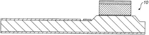
图3是在图1中的截面(B-B)的示意性表示,其示出通过本发明的方法形成的所产生的像素2。在所有下面的附图中,根据图1的截面B-B来表示像素2,虽然应理解,像素2实际上被限定为两半,如在图2的表示中示出的。像素在整个沟槽16上被镜像,沟槽16被蚀刻到IR晶片8中,如将在下面描述的。Figure 3 is a schematic representation of a section (B-B) in Figure 1 showing the
从图3中可看到,用于支撑盖晶片10的键合框架11的结构被设置到像素2的侧面。有盖的FPA 1起初是三个单独的晶片:ROIC晶片9、包括热敏电阻材料3的IR晶片12和盖晶片10。IR晶片12和ROIC晶片9通过热敏电阻材料3的转移键合来接合,以形成像素2,接着使用适当的键合方法例如Cu-Sn键合由盖晶片10将其密封,以将它键合到键合框架11。As can be seen in FIG. 3 , structures for supporting the
ROIC晶片9使用标准CMOS处理技术来预先制造,该技术是公知的,因此不进一步在这里描述。然而,在ROIC晶片9的顶表面13上示出不规则性,以说明可能从标准CMOS处理产生的一般顶表面的表面形貌。The ROIC
在本例中通过使用具有BOX层14和设备层的标准绝缘体上硅(SOI)晶片12来产生IR晶片8,所述设备层具有适合于在形成传感材料3的层堆栈中的第一高掺杂p+Si层的厚度。当然,任何适当的载体可代替SOI晶片来使用。层的其余部分——包括所需的掺杂层——通过单晶Si和SiGe的外延生长来构造,以在未图案化的SOI晶片的顶部上产生量子阱。这些量子阱层因而提供IR敏感的热敏电阻材料3。可根据性能需要来使用单个或多个量子阱层。The
在IR晶片12中使用的热敏电阻材料3优选地基于在US 6292089中描述的材料概念,并由单晶Si和SiGe量子阱层组成。该热敏电阻3的材料具有高温电阻系数以及低噪声特性,且完全与标准CMOS过程兼容。在量子阱层结构的两侧上使用高掺杂P+Si层(在1019cm-3左右),以向热敏电阻3提供欧姆接触。此外,未掺杂Si势垒层必须存在于高掺杂P+Si层和量子阱层之间。SOI晶片及其形成在本领域中是公知的。在本发明的这个例子中,设置在SOI晶片12的BOX层14之上的所有层的总厚度应是波长优化的,其对于本发明将理想地是大约0.5到0.7μm。The
现在将参考单个像素2详细描述本发明的制造过程,虽然应理解,可使用这个方法在阵列中同时形成多个像素。The fabrication process of the present invention will now be described in detail with reference to a
图4示出用于处理IR晶片8以限定像素2并构造支撑腿7的步骤,如下所述。首先,IR晶片8被设置(a),如上所述。薄膜金属层例如AlSi或TiAl被沉积(b)以充当反射层5,反射层5也用于欧姆接触。有效地将像素2分成两半的沟槽16接着被蚀刻(c)穿过反射层5,并进入热敏电阻3中。接着,通过蚀刻(d)穿过反射层5、热敏电阻3和SOI晶片的BOX层14来界定像素2的区域。接着绝缘材料例如Al2O3的薄层优选地通过原子层沉积(ALD)被沉积(e),以形成第一电绝缘层17,使被蚀刻到热敏电阻3中的沟渠16的垂直侧壁绝缘。在此之后,通过例如等离子体增强化学气相沉积(PECVD)来沉积一层低温氧化物18(f),接着通过抛光来使其平面化。通过蚀刻(g)穿过第一低温氧化物层18和它下面的绝缘层17来打开腿7的接触窗口19,且薄膜材料被沉积(h)并被图案化,以形成像素的腿7.进一步低温氧化物被沉积(i)在表面上,如以前一样,并接着通过抛光而被平面化(j)。Figure 4 shows the steps used to process the
如上所述,腿7的材料必须被选择成提供足够的机械强度以支撑像素2,确保良好的电连接,同时防止经由腿7在像素2和ROIC晶片9上的ROIC之间的热传导。该材料也必须经受得住牺牲氧化层的随后蚀刻,以释放像素2。腿7的适当材料的例子是非晶形TiAl。As mentioned above, the material of the legs 7 must be chosen to provide sufficient mechanical strength to support the
图5示出IR晶片8的处理如何继续形成第一传导部分25,第一传导部分25与腿7物理接触,如下所述。首先,通过蚀刻穿过牺牲氧化层18打开腿7的接触窗口22(a),且接着薄金属层23例如TiW/Cu被沉积(b)在IR晶片的表面上。该金属层23用作用于接下来的电镀的籽晶和粘结剂,由此良好的导体材料24例如铜(Cu)被电镀在IR晶片8的表面上。随后,暴露在牺牲氧化层18的表面之上的任何传导材料24通过抛光被移除(d)。因此,导体材料24只保留在接触窗口22中,形成与下面的腿7接触的第一传导部分25。此时,IR晶片8准备被键合到ROIC晶片9。Figure 5 shows how processing of the
图6示出用于制备用于键合的预先制造的ROIC晶片的步骤。首先,例如Al2O3的薄绝缘层26优选地通过原子层沉积(ALD)被沉积在ROIC晶片9的表面上(b)。该绝缘层26将被用作蚀刻阻挡层来阻挡在随后阶段使用的气相HF,以释放像素2。然而,该绝缘层26需要从金属ROIC衬垫21移除,且因此它通过光刻术被图案化并被蚀刻。蚀刻应在下面的金属ROIC衬垫21处停止,但选择性一般在这个步骤不是关键的(通常使用的ROIC衬垫材料是AlSi、AlCu或AlSiCu)。Figure 6 shows the steps used to prepare a prefabricated ROIC wafer for bonding. First, a thin insulating
在上面的过程步骤之后,低温氧化物层27使用例如等离子体增强化学气相沉积(PECVD)被沉积(c)在ROIC晶片9上,并接着被抛光以使其平面化。类似于在IR晶片上的第一传导部分的形成,接着通过蚀刻穿过氧化物层27打开到ROIC衬垫21的接触窗口28(d)。类似于设置在IR晶片8上的金属层23的薄金属层29接着被沉积在ROIC晶片9的表面上。随后,在牺牲氧化物层27的表面上暴露的任何导体材料30通过抛光被移除之前,良好的导体材料30例如铜(Cu)被电镀在ROIC晶片9的整个表面上。因此,导体材料30只保留在以前蚀刻的接触窗口28中,形成与ROIC晶片9的下面的金属ROIC衬垫21接触的第二传导部分31。此时,ROIC晶片9准备被键合到IR晶片8。After the above process steps, a low
可选的过程是首先通过使用例如PECVD沉积具有比晶片表面13的表面形貌更大的厚度的低温氧化物来平面化ROIC晶片9的表面。该氧化物层被抛光,以在接触孔蚀穿它,直到ROIC金属衬垫21之前使其平面化。随后,金属层可被沉积并图案化,以在ROIC金属衬垫21的顶部上创建第二传导部分31,且上述方法的步骤(b)到(g)接着发生。在这个可选的过程中,绝缘层26被沉积在平面化的表面上,而不是具有表面不规则13的表面上。An optional procedure is to first planarize the surface of the
另一可选的过程是记录该过程,使得在步骤(b)中绝缘层的图案结构替代地与步骤(d)组合,在(c)之后,作为双蚀刻过程,使得ALD层的图案可在接触窗口被打开之后完成。Another optional procedure is to record the process such that the patterning of the insulating layer in step (b) is instead combined with step (d), after (c), as a double etching process such that the patterning of the ALD layer can be Finished after the contact window is opened.
图7示出通过使用转移键合过程接合在一起的IR晶片8和ROIC晶片9,在此期间,两个晶片8、9被键合在一起,且IR敏感的热敏电阻层3和反射层5被转移到ROIC晶片。在这两个晶片8、9(由虚线示出)之间的键合界面由SiO2和第一传导部分25的传导材料24和第二传导部分31的传导材料30组成,该材料在本例中是Cu。晶片键合可因此是热压缩金属键合和在低于400°C的温度处执行的氧化物-氧化物键合。然而,当氧化物18、27以后在像素2的释放期间在转移键合过程之后被移除时,在键合界面中形成的所产生的传导接触塞子20之间是金属键合,该键合界面对像素2起作用是必不可少的。Figure 7 shows the
虽然不是必须的,但至少部分地键合氧化物层18、27可能仍然是有利的,理由如下。首先,氧化物-氧化物键合在室温开始,将晶片8、9保持在一起,同时温度斜升,用于热压缩键合。这确保这两个晶片8、9之间的对齐保持在与在室温得到的相同水平处。其次,在所产生的传导接触塞子20中的键合金属25、31的区域很小,且不必一定提供足够的强度来经受得住在随后的研磨期间增强的剪切力,以移除牺牲的IR晶片8。Although not required, it may nevertheless be advantageous to at least partially bond the oxide layers 18, 27 for the following reasons. First, oxide-oxide bonding starts at room temperature, holding the
可选的过程可分别用于传导部分25和31以及IR晶片和ROIC的晶片键合界面的形成,这也落在本发明的范围内。在这个备选方案中,金属部分25和31的金属沉积和图案化被首先执行。氧化物层接着被沉积,并接着被抛光以使其平面化,使得暴露在金属部分的表面上的任何氧化物材料被移除。在这种情况下,键合界面构成SiO2的阱以及第一传导部分25和第二传导部分31的传导材料的阱。Alternative processes may be used for the formation of the
图8示出在热敏电阻材料的转移键合之后完成像素2的制备过程的步骤,如下所述。用于创建IR晶片8的原始载体晶片12的牺牲处理层15优选地通过研磨和/或蚀刻而被移除,随后移除绝缘层17。原始SOI晶片12的BOX氧化物层14接着被移除(c)。最后,薄膜材料被沉积,例如MoSi2或TiAl,以充当电磁频谱在7-14μm范围内的吸收层4。吸收层4接着被图案化。Figure 8 shows the steps in the process of completing the fabrication of the
图9示出在ROIC晶片9上形成的键合框架11,所述键合框架11被布置成环绕焦平面阵列1的周围,以使它准备由盖晶片10进行封装。键合框架11以如下过程形成。FIG. 9 shows the
首先,保护氧化物层32被沉积并图案化(a),使得它覆盖像素2的区域,以保护它们免受接下来的金属层34的沉积(如下将解释的)。接着,接触窗口33被蚀刻(b)穿过氧化物层32,直到绝缘层26,绝缘层以前在其制备期间被沉积在ROIC晶片9上。薄金属层34接着被沉积(c)在ROIC晶片9的表面上,类似于分别在IR晶片8和ROIC晶片9的制备期间沉积在IR晶片8和ROIC晶片9上的金属层23、29。First, a
随后,在形成键合框架的适当的材料36、37例如Cu和Sn被电镀(d)到接触窗口33内的ROIC晶片9的表面上,以形成键合框架11之前,厚电镀抗蚀剂35被沉积和图案化。最后,电镀抗蚀剂35和暴露的金属层34被移除(e),留下键合框架11准备接纳盖晶片10。Subsequently, a thick plating resist 35 is applied before
在限定像素2中的最后步骤是移除牺牲氧化物层18、27,以释放像素2,如图11所示。优选地使用无水气相HF移除牺牲氧化物层18、27,无水气相HF与所有暴露的材料兼容。在释放像素2之后,FPA1准备进行盖键合。假定在盖键合的时刻像素2已被释放,由于FPA1的易碎性,不允许晶片的湿化学处理。The final step in defining the
图11示出形成盖晶片10的步骤,所述盖晶片10用于在真空下封装FPA1,以减小远离像素2的传热。需要用于焦平面阵列1的密封真空封装的盖晶片10来传输入射IR波。Si和Ge都展示在所关注的波长范围内的高透光率,且因此都适合于这个目的。然而,Ge的热膨胀系数与Si的热膨胀系数相比更高,这将导致在所键合的材料中引起高热残余应力,因此Si是优选的选择。选择盖晶片10的厚度是在最小化吸收的需要和在处理期间的安全操作之间的折衷,在最小化吸收中,晶片越薄越好。盖晶片10可以如下步骤形成。FIG. 11 shows the steps of forming the
首先,腔36被蚀刻(a)到盖晶片中,这由于很多原因而完成,例如:适应焦平面阵列的功能所需的不同薄膜,如下所述;处理由大气压力从盖的顶侧压迫而产生的盖晶片的弯曲;以及提供在线键合衬垫之上的足够距离,这些键合衬垫设置在密封盖(未示出)外部,以为了释放这些衬垫而允许随后被锯开。First, the
抗反射涂层37接着沉积(b)在盖晶片10的一侧或两侧上,以最小化IR辐射的反射。在所示例子中,涂层37被沉积在盖晶片10的两侧上。长波通带(LWP)滤波器也可设置在盖晶片10的表面上,优选地作为抗反射涂层37的部分,以阻挡短波长并防止通过直接暴露于阳光而加热像素2。理论上仅在盖晶片10的外部顶表面上需要LWP滤波器。An
然而,在盖晶片10的两侧上的层中的差异可能引入相当大的应力,并因此使盖晶片10弯曲。如果严重,这个弯曲将阻止盖晶片10键合。LWP滤波器和抗反射涂层37因此都优选地沉积在盖晶片10的表面上。在盖晶片10的下侧上,涂层37和滤波器可被图案化,使得它从待键合的区域被移除。However, differences in the layers on both sides of the
接着,可选的图案化薄膜非蒸发吸气剂38例如通过荫罩掩膜技术被沉积(c),以将潜在的残余气体截留在键合腔内,并从而在FPA的整个寿命时间内确保所需的真空水平。在吸气剂对IR辐射不是透明的情况下,吸气剂38不应被放置在有源像素2上。因此,它位于盲参考像素和ROIC电子设备之上。类似于在ROIC晶片9上的键合框架11的形成,薄金属层39例如TiW/Cu被沉积(d)在盖晶片10的未蚀刻的凸出部分上,以在厚电镀光致抗蚀剂40被沉积和图案化(e)之前充当粘结剂和籽晶。最后,将形成键合框架的金属层——在本例中是Cu和Sn或仅仅Cu——被电镀(f)到盖晶片10的表面上,以限定在盖晶片上的键合框架41,这之后是光致抗蚀剂40和薄金属层39的移除。Next, an optional patterned thin-
如上所述,盖晶片10在真空下通过将盖晶片10上的键合框架41键合到设置在ROIC晶片9上的键合框架11来封装焦平面阵列1,以密封焦平面阵列1内的像素2。As described above, the
虽然在上面的例子中讨论了单独的焦平面阵列1的制造,本发明的方法优选地用于制造在单个ROIC晶片9上的多个焦平面阵列,其可接着在被切成多个单独的焦平面阵列之前,使用适当的密封方法例如Cu-Sn键合(虽然其它方法例如Au-Sn键合同样是可应用的)在晶片级被单个盖晶片10封装。本发明的方法因此在切成小方块之前通过晶片级封装实现设备的更有效和可靠的制造。Although in the above example the fabrication of a single focal plane array 1 was discussed, the method of the present invention is preferably used to fabricate multiple focal plane arrays on a
Claims (12)
Applications Claiming Priority (3)
| Application Number | Priority Date | Filing Date | Title |
|---|---|---|---|
| EP10155249A EP2363887A1 (en) | 2010-03-02 | 2010-03-02 | Focal plane array and method for manufacturing the same |
| EP10155249.5 | 2010-03-02 | ||
| PCT/EP2011/053050 WO2011107487A1 (en) | 2010-03-02 | 2011-03-01 | Focal plane array and method for manufacturing the same |
Publications (1)
| Publication Number | Publication Date |
|---|---|
| CN102893401A true CN102893401A (en) | 2013-01-23 |
Family
ID=42224424
Family Applications (1)
| Application Number | Title | Priority Date | Filing Date |
|---|---|---|---|
| CN2011800120012A Pending CN102893401A (en) | 2010-03-02 | 2011-03-01 | Focal plane array and manufacturing method thereof |
Country Status (6)
| Country | Link |
|---|---|
| US (1) | US8999813B2 (en) |
| EP (2) | EP2363887A1 (en) |
| CN (1) | CN102893401A (en) |
| CA (1) | CA2791337A1 (en) |
| RU (1) | RU2568946C2 (en) |
| WO (1) | WO2011107487A1 (en) |
Cited By (1)
| Publication number | Priority date | Publication date | Assignee | Title |
|---|---|---|---|---|
| CN112951947A (en) * | 2019-11-27 | 2021-06-11 | 原子能和替代能源委员会 | Method for manufacturing a detection device for transferring and directly bonding thin layers containing getter materials |
Families Citing this family (13)
| Publication number | Priority date | Publication date | Assignee | Title |
|---|---|---|---|---|
| US10090349B2 (en) * | 2012-08-09 | 2018-10-02 | Taiwan Semiconductor Manufacturing Company, Ltd. | CMOS image sensor chips with stacked scheme and methods for forming the same |
| US9427776B2 (en) * | 2012-08-23 | 2016-08-30 | Raytheon Company | Method of stress relief in anti-reflective coated cap wafers for wafer level packaged infrared focal plane arrays |
| DE102012217154A1 (en) | 2012-09-24 | 2014-03-27 | Robert Bosch Gmbh | Semiconductor device and method of manufacturing a semiconductor device |
| CN102942158B (en) * | 2012-11-05 | 2017-05-31 | 上海集成电路研发中心有限公司 | The manufacture method of detecting structure |
| JP6161258B2 (en) * | 2012-11-12 | 2017-07-12 | キヤノン株式会社 | Solid-state imaging device, manufacturing method thereof, and camera |
| CN104823030A (en) * | 2012-11-26 | 2015-08-05 | 松下知识产权经营株式会社 | Infrared detection device |
| US9142465B1 (en) | 2013-03-13 | 2015-09-22 | Sandia Corporation | Precise annealing of focal plane arrays for optical detection |
| US10117180B2 (en) | 2013-09-27 | 2018-10-30 | Sony Corporation | Communications device and method |
| CN104515601B (en) * | 2013-10-08 | 2017-06-27 | 黄川� | Platinum electrode negative tempperature coefficient thermistor hemisphere microballon infrared focal plane array panel |
| CN107710021B (en) | 2015-07-09 | 2019-09-27 | 深圳帧观德芯科技有限公司 | Method for making semiconductor X-ray detector |
| FR3070096B1 (en) | 2017-08-08 | 2021-09-17 | Commissariat Energie Atomique | METHOD OF MANUFACTURING A DETECTION DEVICE WITH TWO SUBSTRATES AND SUCH A DETECTION DEVICE |
| US10847569B2 (en) * | 2019-02-26 | 2020-11-24 | Raytheon Company | Wafer level shim processing |
| TWM624413U (en) * | 2021-10-27 | 2022-03-11 | 鴻海精密工業股份有限公司 | Floating bridge structure and infrared sensing device |
Citations (7)
| Publication number | Priority date | Publication date | Assignee | Title |
|---|---|---|---|---|
| EP0773436A2 (en) * | 1995-11-13 | 1997-05-14 | Rockwell International Corporation | Suspended microstructures |
| US6144030A (en) * | 1997-10-28 | 2000-11-07 | Raytheon Company | Advanced small pixel high fill factor uncooled focal plane array |
| WO2001009948A1 (en) * | 1999-08-02 | 2001-02-08 | Honeywell Inc. | Dual wafer attachment process |
| WO2001054189A1 (en) * | 2000-01-17 | 2001-07-26 | Kaelvesten Edouard | Method of joining components |
| US6690014B1 (en) * | 2000-04-25 | 2004-02-10 | Raytheon Company | Microbolometer and method for forming |
| GB2411521A (en) * | 2004-02-27 | 2005-08-31 | Qinetiq Ltd | Fabrication method for micro-sensor device |
| DE102006019080B3 (en) * | 2006-04-25 | 2007-08-30 | Fraunhofer-Gesellschaft zur Förderung der angewandten Forschung e.V. | Housing manufacturing method for e.g. infrared sensor, involves enclosing electrical circuit along metal frame, where circuit is isolated along isolating contour that does not cut surface of substrate |
Family Cites Families (9)
| Publication number | Priority date | Publication date | Assignee | Title |
|---|---|---|---|---|
| SE505753C3 (en) | 1996-01-11 | 1997-10-06 | Imc Ind Mikroelektronikcentrum | Structures for temperature sensors and infrared detectors |
| US6329649B1 (en) * | 1998-10-07 | 2001-12-11 | Raytheon Company | Mm-wave/IR monolithically integrated focal plane array |
| US6667479B2 (en) * | 2001-06-01 | 2003-12-23 | Raytheon Company | Advanced high speed, multi-level uncooled bolometer and method for fabricating same |
| US6890834B2 (en) * | 2001-06-11 | 2005-05-10 | Matsushita Electric Industrial Co., Ltd. | Electronic device and method for manufacturing the same |
| JP2003106895A (en) * | 2001-10-01 | 2003-04-09 | Nec Corp | Thermal infrared detecting element and method of manufacturing the same |
| JP3944465B2 (en) * | 2003-04-11 | 2007-07-11 | 三菱電機株式会社 | Thermal infrared detector and infrared focal plane array |
| US7718967B2 (en) * | 2005-01-26 | 2010-05-18 | Analog Devices, Inc. | Die temperature sensors |
| US8634005B2 (en) * | 2008-09-30 | 2014-01-21 | Drs Rsta, Inc. | Very small pixel pitch focal plane array and method for manufacturing thereof |
| RU82934U1 (en) * | 2009-02-11 | 2009-05-10 | Владимир Артурович Юрьев | BOLOMETRIC RADIATION RECEIVER |
-
2010
- 2010-03-02 EP EP10155249A patent/EP2363887A1/en not_active Withdrawn
-
2011
- 2011-03-01 WO PCT/EP2011/053050 patent/WO2011107487A1/en not_active Ceased
- 2011-03-01 CA CA2791337A patent/CA2791337A1/en not_active Abandoned
- 2011-03-01 EP EP11711790A patent/EP2543071A1/en not_active Withdrawn
- 2011-03-01 RU RU2012141154/28A patent/RU2568946C2/en not_active IP Right Cessation
- 2011-03-01 US US13/582,120 patent/US8999813B2/en not_active Expired - Fee Related
- 2011-03-01 CN CN2011800120012A patent/CN102893401A/en active Pending
Patent Citations (8)
| Publication number | Priority date | Publication date | Assignee | Title |
|---|---|---|---|---|
| EP0773436A2 (en) * | 1995-11-13 | 1997-05-14 | Rockwell International Corporation | Suspended microstructures |
| US6144030A (en) * | 1997-10-28 | 2000-11-07 | Raytheon Company | Advanced small pixel high fill factor uncooled focal plane array |
| WO2001009948A1 (en) * | 1999-08-02 | 2001-02-08 | Honeywell Inc. | Dual wafer attachment process |
| CN1377512A (en) * | 1999-08-02 | 2002-10-30 | 霍尼韦尔有限公司 | Dual water attachment process |
| WO2001054189A1 (en) * | 2000-01-17 | 2001-07-26 | Kaelvesten Edouard | Method of joining components |
| US6690014B1 (en) * | 2000-04-25 | 2004-02-10 | Raytheon Company | Microbolometer and method for forming |
| GB2411521A (en) * | 2004-02-27 | 2005-08-31 | Qinetiq Ltd | Fabrication method for micro-sensor device |
| DE102006019080B3 (en) * | 2006-04-25 | 2007-08-30 | Fraunhofer-Gesellschaft zur Förderung der angewandten Forschung e.V. | Housing manufacturing method for e.g. infrared sensor, involves enclosing electrical circuit along metal frame, where circuit is isolated along isolating contour that does not cut surface of substrate |
Cited By (2)
| Publication number | Priority date | Publication date | Assignee | Title |
|---|---|---|---|---|
| CN112951947A (en) * | 2019-11-27 | 2021-06-11 | 原子能和替代能源委员会 | Method for manufacturing a detection device for transferring and directly bonding thin layers containing getter materials |
| CN112951947B (en) * | 2019-11-27 | 2024-04-09 | 原子能和替代能源委员会 | Method for manufacturing a detection device for transferring and directly bonding a thin layer containing a getter material |
Also Published As
| Publication number | Publication date |
|---|---|
| US8999813B2 (en) | 2015-04-07 |
| EP2363887A1 (en) | 2011-09-07 |
| WO2011107487A1 (en) | 2011-09-09 |
| US20130026592A1 (en) | 2013-01-31 |
| RU2568946C2 (en) | 2015-11-20 |
| RU2012141154A (en) | 2014-04-10 |
| EP2543071A1 (en) | 2013-01-09 |
| CA2791337A1 (en) | 2011-09-09 |
Similar Documents
| Publication | Publication Date | Title |
|---|---|---|
| US8999813B2 (en) | Focal plane array and method for manufacturing the same | |
| CN102884627B (en) | Uncooled ir detector and the method for the manufacture of uncooled ir detector | |
| US9258894B2 (en) | Bolometer and preparation method thereof | |
| JP2008070353A (en) | Temperature sensor and manufacturing method thereof | |
| JP2012505373A (en) | Electromagnetic radiation detector with microencapsulation and apparatus for detecting electromagnetic radiation using such a detector | |
| US20150206908A1 (en) | Focal plane array and method for manufacturing the same | |
| CN113767063A (en) | Heterogeneous integration of complementary metal-oxide-semiconductor and MEMS sensors | |
| Lapadatu et al. | High-performance long wave infrared bolometer fabricated by wafer bonding | |
| CN212539430U (en) | Heterogeneously integrated thermal infrared sensing element and thermal infrared sensor | |
| US12484444B2 (en) | Integrated thermal sensor and manufacturing process thereof | |
| US20110073978A1 (en) | Infrared imaging device and method for manufacturing same | |
| RU2793118C2 (en) | Method for manufacturing a device with an improved encapsulating structure for detecting electromagnetic radiation | |
| JP2025540806A (en) | Enhanced Area Getter Architecture for Wafer-Level Vacuum Packaged Uncooled Focal Plane Arrays | |
| HK1176745B (en) | Uncooled infrared detector and methods for manufacturing the same | |
| JP2010114379A (en) | Infrared imaging element, and method of manufacturing the same |
Legal Events
| Date | Code | Title | Description |
|---|---|---|---|
| C06 | Publication | ||
| PB01 | Publication | ||
| C10 | Entry into substantive examination | ||
| SE01 | Entry into force of request for substantive examination | ||
| C02 | Deemed withdrawal of patent application after publication (patent law 2001) | ||
| WD01 | Invention patent application deemed withdrawn after publication |
Application publication date: 20130123 |