CN102761247A - Control circuit of conversion circuit - Google Patents
Control circuit of conversion circuit Download PDFInfo
- Publication number
- CN102761247A CN102761247A CN2011101141944A CN201110114194A CN102761247A CN 102761247 A CN102761247 A CN 102761247A CN 2011101141944 A CN2011101141944 A CN 2011101141944A CN 201110114194 A CN201110114194 A CN 201110114194A CN 102761247 A CN102761247 A CN 102761247A
- Authority
- CN
- China
- Prior art keywords
- circuit
- reference voltage
- feedback
- control
- voltage
- Prior art date
- Legal status (The legal status is an assumption and is not a legal conclusion. Google has not performed a legal analysis and makes no representation as to the accuracy of the status listed.)
- Pending
Links
- 238000006243 chemical reaction Methods 0.000 title claims abstract description 56
- 238000001514 detection method Methods 0.000 claims abstract description 12
- 238000010586 diagram Methods 0.000 description 6
- 239000003990 capacitor Substances 0.000 description 5
- 230000000694 effects Effects 0.000 description 2
- 238000000034 method Methods 0.000 description 2
- 230000005669 field effect Effects 0.000 description 1
- 230000007257 malfunction Effects 0.000 description 1
- 238000006467 substitution reaction Methods 0.000 description 1
Images


Classifications
-
- H—ELECTRICITY
- H02—GENERATION; CONVERSION OR DISTRIBUTION OF ELECTRIC POWER
- H02M—APPARATUS FOR CONVERSION BETWEEN AC AND AC, BETWEEN AC AND DC, OR BETWEEN DC AND DC, AND FOR USE WITH MAINS OR SIMILAR POWER SUPPLY SYSTEMS; CONVERSION OF DC OR AC INPUT POWER INTO SURGE OUTPUT POWER; CONTROL OR REGULATION THEREOF
- H02M3/00—Conversion of DC power input into DC power output
- H02M3/02—Conversion of DC power input into DC power output without intermediate conversion into AC
- H02M3/04—Conversion of DC power input into DC power output without intermediate conversion into AC by static converters
- H02M3/10—Conversion of DC power input into DC power output without intermediate conversion into AC by static converters using discharge tubes with control electrode or semiconductor devices with control electrode
- H02M3/145—Conversion of DC power input into DC power output without intermediate conversion into AC by static converters using discharge tubes with control electrode or semiconductor devices with control electrode using devices of a triode or transistor type requiring continuous application of a control signal
- H02M3/155—Conversion of DC power input into DC power output without intermediate conversion into AC by static converters using discharge tubes with control electrode or semiconductor devices with control electrode using devices of a triode or transistor type requiring continuous application of a control signal using semiconductor devices only
- H02M3/156—Conversion of DC power input into DC power output without intermediate conversion into AC by static converters using discharge tubes with control electrode or semiconductor devices with control electrode using devices of a triode or transistor type requiring continuous application of a control signal using semiconductor devices only with automatic control of output voltage or current, e.g. switching regulators
-
- H—ELECTRICITY
- H02—GENERATION; CONVERSION OR DISTRIBUTION OF ELECTRIC POWER
- H02M—APPARATUS FOR CONVERSION BETWEEN AC AND AC, BETWEEN AC AND DC, OR BETWEEN DC AND DC, AND FOR USE WITH MAINS OR SIMILAR POWER SUPPLY SYSTEMS; CONVERSION OF DC OR AC INPUT POWER INTO SURGE OUTPUT POWER; CONTROL OR REGULATION THEREOF
- H02M1/00—Details of apparatus for conversion
- H02M1/0003—Details of control, feedback or regulation circuits
- H02M1/0025—Arrangements for modifying reference values, feedback values or error values in the control loop of a converter
Landscapes
- Engineering & Computer Science (AREA)
- Power Engineering (AREA)
- Dc-Dc Converters (AREA)
Abstract
Description
技术领域 technical field
本发明是关于一种转换电路的控制电路,尤指一种降低噪声干扰的转换电路的控制电路。The invention relates to a control circuit of a conversion circuit, in particular to a control circuit of a conversion circuit for reducing noise interference.
背景技术 Background technique
请参见图1,为已知的直流转直流转换电路的电路示意图。直流转直流转换电路为降压转换电路,包含一控制器10、两切换开关M1、M2、一电感L、一电容C、一自举电路(Bootstrap Circuit)BS以及一分压电路VD。分压电路VD侦测降压转换电路的一输出电压Vout,以产生一反馈信号FB。控制器10根据反馈信号FB控制切换开关M1、M2的导通与关断,使转换电路将一输入电源Vin的电压转换成输出电压Vout并稳定于一预定电压。Please refer to FIG. 1 , which is a schematic circuit diagram of a known DC-to-DC conversion circuit. The DC-to-DC conversion circuit is a step-down conversion circuit, including a controller 10, two switches M1, M2, an inductor L, a capacitor C, a bootstrap circuit BS, and a voltage divider circuit VD. The voltage dividing circuit VD detects an output voltage Vout of the step-down conversion circuit to generate a feedback signal FB. The controller 10 controls the on and off of the switches M1 and M2 according to the feedback signal FB, so that the conversion circuit converts the voltage of an input power Vin into an output voltage Vout and stabilizes it at a predetermined voltage.
控制器10包含一比较器12、一固定导通时间电路14及一逻辑控制电路16及两栅极驱动单元18、20。比较器12接收反馈信号FB及一参考电压Vref,以据此产生一反馈控制信号。固定导通时间电路14根据反馈控制信号产生一固定导通信号。逻辑控制电路16根据固定导通信号决定切换开关M1、M2的导通与关断时间点,并透过栅极驱动单元18、20分别导通或关断切换开关M1、M2。而由于切换开关M2为N型金属氧化物半导体场效晶体管开关,而为避免切换开关M2导通时,控制器10中的栅极驱动单元20无法提供足够高的信号准位,而无法确保导通切换开关M2。故透过自举电路BS可确保栅极驱动单元20提供足够高的信号准位使切换开关M2导通。The controller 10 includes a
由于电路本身会存在一些噪声,使比较器12的比较判断会受到噪声干扰而误动作。故比较器12会设计一迟滞量,以避免噪声的干扰。而参考电压Vref为一固定值,故对于不同的输出电压Vout的要求,会改变分压电路VD的分压比值的方式来配合。因此,对越高的输出电压Vout,则分压电路VD的分压比值越小,使上述比较器12的迟滞量反应至输出电压Vout的纹波(VoltageRipple)会越大。Due to the presence of some noise in the circuit itself, the comparison judgment of the
发明内容 Contents of the invention
鉴于先前技术中的避免噪声而设定比较器的迟滞量的方法,会导致不同的输出电压设定会有不同的电压纹波的问题,本发明的目的在于提供一种转换电路的控制电路,以调整参考电压的高低来配合输出电压的高低,可有效降低不同输出电压的纹波大小变化。In view of the method of setting the hysteresis of the comparator to avoid noise in the prior art, it will lead to the problem that different output voltage settings will have different voltage ripples. The purpose of the present invention is to provide a control circuit for a conversion circuit, Adjusting the level of the reference voltage to match the level of the output voltage can effectively reduce the variation of the ripple size of different output voltages.
为达上述目的,本发明提供了一种转换电路的控制电路,用以控制转换电路以将一输入电源的电力转换成一输出电压,而一电压侦测电路根据输出电压产生一反馈信号。转换电路的控制电路包含一参考电压产生电路、一参考电压调整电路、一反馈电路以及一驱动电路。参考电压产生电路用以产生一参考电压。参考电压调整电路调整参考电压以产生一调整参考电压。反馈电路根据调整参考电压及反馈信号产生一反馈控制信号。驱动电路根据反馈控制信号产生至少一控制信号以控制转换电路。To achieve the above object, the present invention provides a control circuit for a conversion circuit, which is used to control the conversion circuit to convert an input power supply into an output voltage, and a voltage detection circuit generates a feedback signal according to the output voltage. The control circuit of the converting circuit includes a reference voltage generating circuit, a reference voltage adjusting circuit, a feedback circuit and a driving circuit. The reference voltage generating circuit is used for generating a reference voltage. The reference voltage adjusting circuit adjusts the reference voltage to generate an adjusted reference voltage. The feedback circuit generates a feedback control signal according to the adjusted reference voltage and the feedback signal. The drive circuit generates at least one control signal to control the conversion circuit according to the feedback control signal.
本发明也提供一种转换电路的控制电路,用以控制转换电路以将一输入电源的电力转换成一输出电压,而一电压侦测电路根据输出电压产生一反馈信号。转换电路的控制电路包含一参考电压产生电路、一参考电压调整电路、一反馈电路及一驱动电路。参考电压产生电路用以产生一参考电压。参考电压调整电路耦接参考电压产生电路以调整参考电压的准位。反馈电路根据参考电压及反馈信号产生一反馈控制信号。驱动电路根据反馈控制信号产生至少一控制信号以控制转换电路。The present invention also provides a control circuit of the conversion circuit, which is used to control the conversion circuit to convert the power of an input power supply into an output voltage, and a voltage detection circuit generates a feedback signal according to the output voltage. The control circuit of the conversion circuit includes a reference voltage generation circuit, a reference voltage adjustment circuit, a feedback circuit and a drive circuit. The reference voltage generating circuit is used for generating a reference voltage. The reference voltage adjusting circuit is coupled to the reference voltage generating circuit to adjust the level of the reference voltage. The feedback circuit generates a feedback control signal according to the reference voltage and the feedback signal. The drive circuit generates at least one control signal to control the conversion circuit according to the feedback control signal.
本发明以调整参考电压的高低来配合输出电压的高低,可有效降低不同输出电压的纹波大小变化。The present invention adjusts the level of the reference voltage to match the level of the output voltage, which can effectively reduce the variation of ripples of different output voltages.
以上的概述与接下来的详细说明皆为示范性质,是为了进一步说明本发明的申请专利范围。而有关本发明的其它目的与优点,将在后续的说明与附图加以阐述。The above summary and the following detailed description are exemplary in nature, and are intended to further illustrate the patent scope of the present invention. Other purposes and advantages of the present invention will be described in the subsequent description and accompanying drawings.
附图说明 Description of drawings
图1为已知的直流转直流转换电路的电路示意图;FIG. 1 is a schematic circuit diagram of a known DC-to-DC conversion circuit;
图2为根据本发明的一第一较佳实施例的直流转直流转换电路的电路示意图;2 is a schematic circuit diagram of a DC-to-DC conversion circuit according to a first preferred embodiment of the present invention;
图3为根据本发明的一第二较佳实施例的直流转直流转换电路的电路示意图。FIG. 3 is a schematic circuit diagram of a DC-to-DC conversion circuit according to a second preferred embodiment of the present invention.
【主要组件符号说明】[Description of main component symbols]
先前技术:Prior Art:
控制器10controller 10
比较器12
固定导通时间电路14Fixed On-
逻辑控制电路16
栅极驱动单元18、20
切换开关M1、M2Switch M1, M2
电感LInductance L
电容CCapacitance C
自举电路BSBootstrap circuit BS
分压电路VDVoltage divider circuit VD
输出电压VoutOutput voltage Vout
反馈信号FBFeedback signal FB
输入电源VinInput power Vin
参考电压VrefReference voltage Vref
本发明:this invention:
控制器100、200
参考电压调整电路102、202Reference
电压侦测电路104、204
驱动电路110、210
反馈电路112、212
固定时间电路114Fixed Time Circuit 114
参考电压产生电路115、215Reference
逻辑控制电路116
栅极驱动单元118、120
切换开关M1、M2Switch M1, M2
电感LInductance L
电容CCapacitance C
自举电路BSBootstrap circuit BS
输入电源VinInput power Vin
输出电压VoutOutput voltage Vout
反馈信号FBFeedback signal FB
参考电压Vr0、Vr’Reference voltage Vr0, Vr'
调整参考电压VrAdjust the reference voltage Vr
电阻RV、RV1、RV2Resistors RV, RV1, RV2
二极管DDiode D
具体实施方式 Detailed ways
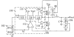
请参见图2,为根据本发明的一第一较佳实施例的直流转直流转换电路的电路示意图。转换电路包含一转换控制电路及一转换电路,其中转换控制电路包含一控制器100及一参考电压调整电路102。在本实施例,转换电路包含两切换开关M1、M2、一电感L、一电容C及一自举电路BS。两切换开关M1、M2根据控制器100的控制于导通状态及关断状态之间切换,以将一输入电源Vin的电力经电感L及电容C后转换成一输出电压Vout。一电压侦测电路104耦接转换电路,以根据输出电压Vout产生一反馈信号FB。Please refer to FIG. 2 , which is a schematic circuit diagram of a DC-to-DC conversion circuit according to a first preferred embodiment of the present invention. The conversion circuit includes a conversion control circuit and a conversion circuit, wherein the conversion control circuit includes a
控制器100包含一参考电压产生电路115、一反馈电路112以及一驱动电路110,其中驱动电路110包含一固定时间电路114及一逻辑控制电路116及两栅极驱动单元118、120。参考电压产生电路115用以产生一参考电压Vr0。参考电压调整电路102调整参考电压Vr0以产生一调整参考电压Vr。反馈电路112根据调整参考电压Vr及反馈信号FB产生一反馈控制信号。驱动电路110根据反馈控制信号产生至少一控制信号以控制转换电路的切换开关M1、M2的导通与关断。The
在本实施例中,反馈电路112包含一比较器,比较器的非反相端接收调整参考电压Vr,反相端接收反馈信号FB,于反馈信号FB的准位低于调整参考电压Vr的准位时输出一反馈控制信号至固定时间电路114。在本实施例,固定时间电路114为一固定导通时间电路,于接收到反馈控制信号后产生固定时间长度的信号,使逻辑控制电路116据此控制切换开关M2导通固定时间长度以传递输入电源Vin的电力至转换电路。而由于不同的输出电压及输入电压均会影响切换开关M1、M2的工作周期,因此在固定导通时间的情况下,会造成不同的电路有不同的操作频率。本发明的固定时间电路114可根据输出电压Vout及输入电源Vin的电压调整固定时间长度的长短,据此达到定频的效果。In this embodiment, the
本发明的电压侦测电路104原则上不需调整反馈信号FB与输出电压Vout之间的缩放比例,而是透过参考电压调整电路102的功能,随输出电压Vout的高低提供不同的电压。如此,可避免随输出电压Vout的不同,反馈电路112所设定的迟滞量也会被缩放而导致对应的纹波大小不同。在本实施例中,电压侦测电路104为一分压电路,包含串联的两电阻RV1、RV2,其分压值由使用者根据输出电压Vout的高低而设定。In principle, the
请参见图3,为根据本发明的一第二较佳实施例的直流转直流转换电路的电路示意图。转换电路包含一转换控制电路及一转换电路,其中转换控制电路包含一控制器200及一参考电压调整电路202。转换电路包含一切换开关M1、一二极管D、一电感L及一电容C,以将一输入电源Vin的电力经电感L及电容C后转换成一输出电压Vout。一电压侦测电路204耦接转换电路,以根据输出电压Vout产生一反馈信号FB。相较于图2所示的实施例,主要差异说明如下。Please refer to FIG. 3 , which is a schematic circuit diagram of a DC-to-DC conversion circuit according to a second preferred embodiment of the present invention. The conversion circuit includes a conversion control circuit and a conversion circuit, wherein the conversion control circuit includes a
控制器200包含一参考电压产生电路215、一反馈电路212以及一驱动电路210。参考电压调整电路202耦接参考电压产生电路215以调整参考电压产生电路215所产生的一参考电压Vr’的准位。在本实施例中,参考电压调整电路202包含一电阻RV,参考电压产生电路215根据参考电压调整电路202的阻值调整参考电压Vr’的准位。反馈电路212包含一比较器,比较器的反相端接收参考电压Vr’,非反相端接收电压侦测电路204根据输出电压Vout所产生的反馈信号FB,于反馈信号FB的准位高于参考电压Vr’的准位时输出一反馈控制信号至驱动电路210。在本实施例,驱动电路210为一固定关断驱动电路,于接收反馈电路212所产生的反馈控制信号时,关断切换开关M1一固定时间长度,以停止传送输入电源Vin的电力至转换电路。而由于不同的输出电压及输入电压均会影响切换开关M1的工作周期,因此在固定关断时间的情况下,会造成不同的电路有不同的操作频率。本发明的驱动电路210可根据输出电压Vout及输入电源Vin的电压调整固定时间长度的长短,据此达到定频的效果。The
同样地,在本发明的电压侦测电路204原则上不需调整反馈信号FB与输出电压Vout之间的缩放比例,而是透过参考电压调整电路202的功能,以随输出电压Vout的高低提供不同的参考电压,使输出电压Vout的纹波不致因输出电压Vout本身的高低而有所不同。Similarly, in principle, the
如上所述,本发明完全符合专利三要件:新颖性、创造性和产业上的实用性。本发明在上文中已以较佳实施例揭露,然熟悉本项技术者应理解的是,该实施例仅用于描绘本发明,而不应解读为限制本发明的范围。应注意的是,举凡与该实施例等效的变化与置换,均应设为涵盖于本发明的范畴内。因此,本发明的保护范围当以权利要求书所界定的范围为准。As mentioned above, the present invention fully complies with the three requirements of a patent: novelty, creativity and industrial applicability. The present invention has been disclosed above with preferred embodiments, but those skilled in the art should understand that the embodiments are only for describing the present invention, and should not be construed as limiting the scope of the present invention. It should be noted that all changes and substitutions equivalent to this embodiment should be included in the scope of the present invention. Therefore, the protection scope of the present invention shall be determined by the scope defined in the claims.
Claims (10)
Priority Applications (2)
| Application Number | Priority Date | Filing Date | Title |
|---|---|---|---|
| CN2011101141944A CN102761247A (en) | 2011-04-26 | 2011-04-26 | Control circuit of conversion circuit |
| US13/175,946 US20120274294A1 (en) | 2011-04-26 | 2011-07-04 | Controller for converting circuit |
Applications Claiming Priority (1)
| Application Number | Priority Date | Filing Date | Title |
|---|---|---|---|
| CN2011101141944A CN102761247A (en) | 2011-04-26 | 2011-04-26 | Control circuit of conversion circuit |
Publications (1)
| Publication Number | Publication Date |
|---|---|
| CN102761247A true CN102761247A (en) | 2012-10-31 |
Family
ID=47055590
Family Applications (1)
| Application Number | Title | Priority Date | Filing Date |
|---|---|---|---|
| CN2011101141944A Pending CN102761247A (en) | 2011-04-26 | 2011-04-26 | Control circuit of conversion circuit |
Country Status (2)
| Country | Link |
|---|---|
| US (1) | US20120274294A1 (en) |
| CN (1) | CN102761247A (en) |
Families Citing this family (6)
| Publication number | Priority date | Publication date | Assignee | Title |
|---|---|---|---|---|
| US9293989B2 (en) * | 2011-04-21 | 2016-03-22 | Green Solution Technology Co., Ltd. | DC to DC buck converting controller with programmable on-time period unit |
| US10141845B2 (en) * | 2016-04-13 | 2018-11-27 | Texas Instruments Incorporated | DC-DC converter and control circuit with low-power clocked comparator referenced to switching node for zero voltage switching |
| US10177658B2 (en) | 2016-04-14 | 2019-01-08 | Texas Instruments Incorporated | Methods and apparatus for adaptive timing for zero voltage transition power converters |
| US10141846B2 (en) | 2016-04-15 | 2018-11-27 | Texas Instruments Incorporated | Methods and apparatus for adaptive timing for zero voltage transition power converters |
| TW201917999A (en) * | 2017-10-17 | 2019-05-01 | 力智電子股份有限公司 | Power conversion device, time signal generator and method thereof |
| US10840797B2 (en) | 2018-11-26 | 2020-11-17 | Texas Instruments Incorporated | Load release detection circuit |
Citations (5)
| Publication number | Priority date | Publication date | Assignee | Title |
|---|---|---|---|---|
| CN1696860A (en) * | 2004-04-30 | 2005-11-16 | 恩益禧电子股份有限公司 | Voltage regulator with improved power supply rejection ratio characteristics and narrow response band |
| US20070090818A1 (en) * | 2005-10-20 | 2007-04-26 | Fujitsu Limited | Control circuit of DC-DC converter and control method thereof |
| US20100123446A1 (en) * | 2008-11-18 | 2010-05-20 | Dongjie Cheng | Feed-Forward Compensation for a Hysteretic Switching Regulator |
| CN101989814A (en) * | 2009-07-29 | 2011-03-23 | 台达电子工业股份有限公司 | Voltage Regulating Circuit and Its Applicable Parallel Voltage Regulating Circuit System |
| CN102751870A (en) * | 2011-04-21 | 2012-10-24 | 登丰微电子股份有限公司 | DC-DC voltage reduction conversion controller |
-
2011
- 2011-04-26 CN CN2011101141944A patent/CN102761247A/en active Pending
- 2011-07-04 US US13/175,946 patent/US20120274294A1/en not_active Abandoned
Patent Citations (5)
| Publication number | Priority date | Publication date | Assignee | Title |
|---|---|---|---|---|
| CN1696860A (en) * | 2004-04-30 | 2005-11-16 | 恩益禧电子股份有限公司 | Voltage regulator with improved power supply rejection ratio characteristics and narrow response band |
| US20070090818A1 (en) * | 2005-10-20 | 2007-04-26 | Fujitsu Limited | Control circuit of DC-DC converter and control method thereof |
| US20100123446A1 (en) * | 2008-11-18 | 2010-05-20 | Dongjie Cheng | Feed-Forward Compensation for a Hysteretic Switching Regulator |
| CN101989814A (en) * | 2009-07-29 | 2011-03-23 | 台达电子工业股份有限公司 | Voltage Regulating Circuit and Its Applicable Parallel Voltage Regulating Circuit System |
| CN102751870A (en) * | 2011-04-21 | 2012-10-24 | 登丰微电子股份有限公司 | DC-DC voltage reduction conversion controller |
Also Published As
| Publication number | Publication date |
|---|---|
| US20120274294A1 (en) | 2012-11-01 |
Similar Documents
| Publication | Publication Date | Title |
|---|---|---|
| US9935470B2 (en) | System and method for wireless power transfer using a power converter with a bypass mode | |
| US9529373B2 (en) | Switching regulator and control circuit and control method therefor | |
| CN101728947B (en) | Dc-dc converter | |
| CN102751870B (en) | DC-to-DC Buck Converter Controller | |
| CN103066823B (en) | Controller and control method of switch power source | |
| CN107251400A (en) | Many level switch adjuster circuits and method with finite states machine control | |
| CN104052281A (en) | Switching Regulator with Adaptive PWM/PFM Modulator | |
| CN102761255A (en) | Switched-mode power supply | |
| US9000735B2 (en) | DC-DC controller and operation method thereof | |
| CN105075088A (en) | Systems and methods for 100 percent duty cycle in switching regulators | |
| CN102761247A (en) | Control circuit of conversion circuit | |
| US20160149493A1 (en) | Control circuit, control method and switch-type converter | |
| TW201803260A (en) | Switching regulator | |
| TWI551022B (en) | Dynamic drive capability adjustment of the power control device | |
| TWI547083B (en) | Control circuit of power converter and related method | |
| CN105449994B (en) | The control circuit of the power converter | |
| US20140375285A1 (en) | Dc-dc boost converter | |
| JP2010158116A (en) | Dc-dc converter | |
| CN106487222B (en) | Power supply operating in ripple control mode and control method thereof | |
| JP2014112996A (en) | Light load detection circuit, switching regulator, and method of controlling the same | |
| TWI434497B (en) | Controller for converting circuit | |
| CN107394998A (en) | Control circuit, control method and switching power supply | |
| CN103390996B (en) | A control circuit and associated switching regulator | |
| CN102299624B (en) | Switching control circuit and switching power supply circuit | |
| CN103683900B (en) | Control circuit and control method of power converter |
Legal Events
| Date | Code | Title | Description |
|---|---|---|---|
| C06 | Publication | ||
| PB01 | Publication | ||
| C10 | Entry into substantive examination | ||
| SE01 | Entry into force of request for substantive examination | ||
| C02 | Deemed withdrawal of patent application after publication (patent law 2001) | ||
| WD01 | Invention patent application deemed withdrawn after publication |
Application publication date: 20121031 |