CN102736193A - Opto-electric hybrid board and manufacturing method therefor - Google Patents
Opto-electric hybrid board and manufacturing method therefor Download PDFInfo
- Publication number
- CN102736193A CN102736193A CN2012100552722A CN201210055272A CN102736193A CN 102736193 A CN102736193 A CN 102736193A CN 2012100552722 A CN2012100552722 A CN 2012100552722A CN 201210055272 A CN201210055272 A CN 201210055272A CN 102736193 A CN102736193 A CN 102736193A
- Authority
- CN
- China
- Prior art keywords
- mentioned
- optical waveguide
- circuit unit
- unit
- optical element
- Prior art date
- Legal status (The legal status is an assumption and is not a legal conclusion. Google has not performed a legal analysis and makes no representation as to the accuracy of the status listed.)
- Granted
Links
Images




Classifications
-
- G—PHYSICS
- G02—OPTICS
- G02B—OPTICAL ELEMENTS, SYSTEMS OR APPARATUS
- G02B6/00—Light guides; Structural details of arrangements comprising light guides and other optical elements, e.g. couplings
- G02B6/24—Coupling light guides
- G02B6/42—Coupling light guides with opto-electronic elements
- G02B6/4201—Packages, e.g. shape, construction, internal or external details
- G02B6/4202—Packages, e.g. shape, construction, internal or external details for coupling an active element with fibres without intermediate optical elements, e.g. fibres with plane ends, fibres with shaped ends, bundles
-
- G—PHYSICS
- G02—OPTICS
- G02B—OPTICAL ELEMENTS, SYSTEMS OR APPARATUS
- G02B6/00—Light guides; Structural details of arrangements comprising light guides and other optical elements, e.g. couplings
- G02B6/24—Coupling light guides
- G02B6/42—Coupling light guides with opto-electronic elements
- G02B6/4201—Packages, e.g. shape, construction, internal or external details
- G02B6/4219—Mechanical fixtures for holding or positioning the elements relative to each other in the couplings; Alignment methods for the elements, e.g. measuring or observing methods especially used therefor
- G02B6/4228—Passive alignment, i.e. without a detection of the degree of coupling or the position of the elements
- G02B6/423—Passive alignment, i.e. without a detection of the degree of coupling or the position of the elements using guiding surfaces for the alignment
- G02B6/4231—Passive alignment, i.e. without a detection of the degree of coupling or the position of the elements using guiding surfaces for the alignment with intermediate elements, e.g. rods and balls, between the elements
-
- Y—GENERAL TAGGING OF NEW TECHNOLOGICAL DEVELOPMENTS; GENERAL TAGGING OF CROSS-SECTIONAL TECHNOLOGIES SPANNING OVER SEVERAL SECTIONS OF THE IPC; TECHNICAL SUBJECTS COVERED BY FORMER USPC CROSS-REFERENCE ART COLLECTIONS [XRACs] AND DIGESTS
- Y10—TECHNICAL SUBJECTS COVERED BY FORMER USPC
- Y10T—TECHNICAL SUBJECTS COVERED BY FORMER US CLASSIFICATION
- Y10T29/00—Metal working
- Y10T29/49—Method of mechanical manufacture
- Y10T29/49002—Electrical device making
- Y10T29/49117—Conductor or circuit manufacturing
- Y10T29/49124—On flat or curved insulated base, e.g., printed circuit, etc.
- Y10T29/4913—Assembling to base an electrical component, e.g., capacitor, etc.
- Y10T29/49139—Assembling to base an electrical component, e.g., capacitor, etc. by inserting component lead or terminal into base aperture
- Y10T29/4914—Assembling to base an electrical component, e.g., capacitor, etc. by inserting component lead or terminal into base aperture with deforming of lead or terminal
Landscapes
- Physics & Mathematics (AREA)
- General Physics & Mathematics (AREA)
- Optics & Photonics (AREA)
- Optical Integrated Circuits (AREA)
- Optical Couplings Of Light Guides (AREA)
- Semiconductor Lasers (AREA)
- Light Receiving Elements (AREA)
Abstract
Description
技术领域 technical field
本发明涉及一种具有光波导路单元和安装有光学元件的电路单元的光电混载基板及其制造方法。The present invention relates to a photoelectric hybrid substrate having an optical waveguide unit and a circuit unit on which optical elements are mounted and a manufacturing method thereof.
背景技术 Background technique
在最近的电子设备等中,随着传输信息量的增加,除了电布线以外,还采用光布线。即,在上述电子设备等中组装有具有电路单元与光波导路单元的光电混载基板,该电路单元在形成有电布线的电路基板上安装有用于将电信号转换为光信号的发光元件和用于将光信号转换为电信号的受光元件等光学元件;该光波导路单元作为用于传输上述光信号的光布线形成有光波导路。In recent electronic equipment and the like, as the amount of information to be transmitted increases, optical wiring is used in addition to electrical wiring. That is, in the above-mentioned electronic equipment, etc., a photoelectric hybrid board having a circuit unit and an optical waveguide unit mounted on a circuit board on which electrical wiring is formed and a light-emitting element for converting an electrical signal into an optical signal and An optical element such as a light receiving element for converting an optical signal into an electrical signal; the optical waveguide unit is formed with an optical waveguide as an optical wiring for transmitting the above-mentioned optical signal.
作为上述光电混载基板,例如如图15所示,提出了一种在电路单元Eo的光学元件安装面的背面侧与该电路单元Eo呈并列状地设置了光波导路单元Wo的光电混载基板(例如参照专利文献1)。这种类型的光电混载基板将光波导路单元Wo的芯52(光布线)的一端面52a形成为45°的倾斜面,将该芯52的倾斜面形成为光反射面。即,在芯52的一端面(倾斜面)52a处反射光而将光路改变90°,成为能够在芯52与光学元件10之间传递光的状态(参照图示的点划线L)。另外,在图15中,附图标记51是下包层,附图标记53是上包层,附图标记61是光路用的贯通孔。As the above-mentioned photoelectric hybrid substrate, for example, as shown in FIG. 15 , a photoelectric hybrid substrate in which an optical waveguide unit Wo is provided in parallel with the circuit unit Eo on the back side of the optical element mounting surface of the circuit unit Eo has been proposed. Substrate (for example, refer to Patent Document 1). In this type of photoelectric hybrid board, one
在上述光电混载基板中,需要在上述光波导路单元Wo的芯52的一端面(倾斜面)52a处反射从发光元件发射的光、并且在受光元件接收从上述芯52的另一端面(光出口)出射的光。为此,需要对上述光学元件(发光元件、受光元件)10与芯52进行调心。In the photoelectric hybrid substrate, it is necessary to reflect light emitted from the light emitting element at one end surface (inclined surface) 52a of the
因此,一直以来提出有上述光学元件与芯的调心方法。作为其一个例子,有如下方法,即,固定光波导路单元,在从发光元件向该光波导路单元的芯的一端面(光入口)发出光的状态下,改变该发光元件的位置,同时监视从上述芯的另一端面(光出口)出射的光的强度,将该强度最大的位置确定为调心位置(参照专利文献2)。另外,作为另一个例子,有如下方法,即,将形成有定位用的孔部的连接器安装于光波导路单元,将嵌合于上述孔部的定位用的销安装于电路单元,使上述孔部与销相嵌合,由此自动地对光学元件与光波导路单元的芯进行调心(参照专利文献3)。Therefore, the above-mentioned method of aligning the optical element and the core has been proposed all the time. As an example, there is a method of fixing the optical waveguide unit and changing the position of the light emitting element while emitting light from the light emitting element to one end surface (light entrance) of the core of the optical waveguide unit. The intensity of light emitted from the other end surface (light exit) of the core is monitored, and the position where the intensity is the highest is determined as the centering position (see Patent Document 2). In addition, as another example, there is a method of attaching a connector having a positioning hole to the optical waveguide unit, attaching a positioning pin fitted in the hole to the circuit unit, and making the above-mentioned The hole is fitted with the pin, thereby automatically aligning the optical element and the core of the optical waveguide unit (see Patent Document 3).
专利文献1:日本特开2010-192883号公报Patent Document 1: Japanese Patent Laid-Open No. 2010-192883
专利文献2:日本特开平5-196831号公报Patent Document 2: Japanese Patent Application Laid-Open No. 5-196831
专利文献3:日本特开2009-223063号公报Patent Document 3: Japanese Patent Laid-Open No. 2009-223063
但是,在上述专利文献2的调心方法中,虽然能够进行高精度的调心,但是费时费力,量产性欠缺。另外,在上述专利文献3的调心方法中,虽然能够利用孔部与销的嵌合这样的简单方法来进行对位,但是不仅在分别制作连接器及销时产生尺寸误差,还产生连接器相对于光波导路单元的安装位置的位置偏移、定位用的销相对于电路单元的安装位置的位置偏移等,因此这些尺寸误差及位置偏移累积,从而调心精度变差。因此,当欲提高调心精度时,需要进行尺寸精度的管理使得不产生上述尺寸误差、位置偏移,因此成本提高,并且量产性欠缺。However, in the alignment method of the above-mentioned
而且,如上所述,像上述专利文献1那样,在电路单元的光学元件安装面的背面侧与该电路单元呈并列状地设置有光波导路单元的光电混载基板中,为了能够在芯与光学元件之间传递光,需要高精度地将芯的一端面形成为45°的倾斜面(光反射面),并将光路改变90°。但是,在此,由于需要形成上述倾斜面,量产性欠缺。Furthermore, as described above, in the opto-electric hybrid board in which the optical waveguide unit is arranged in parallel with the circuit unit on the rear side of the optical element mounting surface of the circuit unit as in the above-mentioned
发明内容 Contents of the invention
本发明是鉴于这种情况而完成的,其目的在于提供一种不需要进行光波导路单元的芯与电路单元的光学元件的调心作业而且量产性优异、并且即使与电路单元呈并列状地设置光波导路单元、也无需将芯的端面形成为光反射用的倾斜面的光电混载基板及其制造方法。The present invention has been made in view of such circumstances, and its object is to provide an optical waveguide unit that does not require alignment work between the core of the optical waveguide unit and the optical element of the circuit unit, has excellent mass productivity, and can be placed in parallel with the circuit unit. An opto-electric hybrid board and a method for manufacturing the optical waveguide unit without the need to form the end face of the core as an inclined face for light reflection.
为了达到上述目的,本发明的第1技术方案是一种光电混载基板,其是光波导路单元与安装有光学元件的电路单元呈并列状地相结合而成的,其中,上述光波导路单元具有:下包层;光路用的芯,其形成于该下包层的表面;上包层,其用于覆盖该芯;以及电路单元定位用的突起部,其延伸设置于上述下包层及上述上包层的至少一个包层的局部;上述电路单元具有:电路基板;光学元件,其安装于该电路基板;弯折部,其是弯折上述电路基板的光学元件安装部分而成的;以及嵌合孔,其形成于该弯折部并供上述突起部嵌合;上述光波导路单元的上述突起部相对于上述芯的光透过面定位形成在规定位置,上述电路单元的上述光学元件定位安装在上述弯折部的规定位置,形成于该弯折部的上述嵌合孔相对于上述光学元件定位形成在规定位置,上述光波导路单元与上述电路单元的结合是以将上述光波导路单元的上述突起部嵌合于上述电路单元的上述嵌合孔的状态完成的。In order to achieve the above object, the first technical solution of the present invention is a photoelectric hybrid substrate, which is formed by combining an optical waveguide unit and a circuit unit on which an optical element is mounted in parallel, wherein the optical waveguide The unit has: a lower cladding layer; a core for an optical path formed on the surface of the lower cladding layer; an upper cladding layer for covering the core; and a protrusion for positioning a circuit unit extending from the lower cladding layer and a part of at least one cladding layer of the above-mentioned upper cladding layer; the above-mentioned circuit unit has: a circuit substrate; an optical element mounted on the circuit substrate; a bending part formed by bending the optical element mounting part of the above-mentioned circuit substrate and a fitting hole formed in the bent portion for fitting the protrusion; the protrusion of the optical waveguide unit is positioned at a predetermined position relative to the light transmission surface of the core, and the protrusion of the circuit unit is formed at a predetermined position. The optical element is positioned and installed at a predetermined position of the above-mentioned bending part, and the above-mentioned fitting hole formed in the above-mentioned bending part is positioned and formed at a predetermined position relative to the above-mentioned optical element, and the combination of the above-mentioned optical waveguide unit and the above-mentioned circuit unit is to A state in which the protrusion of the optical waveguide unit is fitted into the fitting hole of the circuit unit is completed.
另外,本发明的第2技术方案是上述光电混载基板的制造方法,其是使光波导路单元与安装有光学元件的电路单元呈并列状地相结合的上述光电混载基板的制造方法,其中,上述光波导路单元的制作包括形成下包层的工序、在该下包层的表面形成光路用的芯的工序和以覆盖上述芯的方式形成上包层的工序,在形成上述下包层的工序及形成上述上包层的工序中的至少一个工序中,在相对于上述芯的光透过面进行了定位的规定位置,延伸设置电路单元定位用的突起部,上述电路单元的制作包括形成电路基板的工序和在该电路基板上的规定部分安装光学元件的工序,在形成上述电路基板的工序中,在相对于上述光学元件的预定安装位置进行了定位的规定位置,形成供上述突起部嵌合的嵌合孔,在安装上述光学元件之后,弯折形成相对于该光学元件进行了定位的、包括上述光学元件及上述嵌合孔的规定部分,使上述光波导路单元与上述电路单元相结合而形成光电混载基板是通过将上述光波导路单元的上述突起部嵌合于上述电路单元的上述嵌合孔而完成的。In addition, a second aspect of the present invention is a method of manufacturing the above-mentioned opto-electric hybrid substrate, which is a method of manufacturing the above-mentioned opto-electric hybrid substrate in which an optical waveguide unit and a circuit unit on which an optical element is mounted are combined in parallel, Wherein, the production of the above-mentioned optical waveguide unit includes the steps of forming an under clad layer, the step of forming a core for an optical path on the surface of the under clad layer, and the step of forming an over clad layer so as to cover the core. In at least one of the step of forming the above cladding layer and the step of forming the above cladding layer, a protrusion for positioning the circuit unit is extended at a predetermined position positioned relative to the light transmission surface of the above core, and the production of the above circuit unit Including the process of forming a circuit substrate and the process of mounting an optical element on a predetermined portion of the circuit substrate, in the process of forming the circuit substrate, at a predetermined position positioned relative to a predetermined mounting position of the above optical element, a The fitting hole into which the protrusion is fitted is bent to form a predetermined portion including the optical element and the fitting hole positioned relative to the optical element after mounting the optical element, so that the optical waveguide unit and the The combination of the circuit units to form the opto-electric hybrid board is completed by fitting the protrusions of the optical waveguide unit into the fitting holes of the circuit unit.
本发明的光电混载基板是光波导路单元与安装有光学元件的电路单元呈并列状地相结合而成的。而且,在上述光波导路单元中,芯的光透过面与电路单元定位用的突起部成为相互进行了定位的位置关系。另外,在上述电路单元中,形成有弯折部,在该弯折部的规定位置定位安装有光学元件,并且相对于该光学元件在规定位置形成有供上述突起部嵌合的嵌合孔。因此,在上述光波导路单元的突起部嵌合于上述电路单元的嵌合孔的状态、即、光波导路单元与电路单元相结合的状态下,光波导路单元的芯与电路单元的光学元件成为自动进行了调心的状态。而且,上述嵌合是以光学元件安装部分被弯折的状态(上述弯折部)完成而成为光学元件与芯的光透过面相面对的状态。因此,即使是像本发明这样的、与电路单元呈并列状地设置光波导路单元的光电混载基板,也无需将芯的端面形成为光反射用的倾斜面(无需形成为将光路改变90°的构造)。而且,上述光波导路单元的突起部是延伸设置构成该光波导路单元的下包层及上包层中的至少一个包层的规定部分而成的,上述电路单元的嵌合孔形成于该电路单元,因此上述突起部与上述嵌合孔的嵌合不需要连接器等其他部件。因此,在光波导路单元与电路单元的结合中,不存在上述连接器等其他部件所造成的尺寸误差、位置偏移的累积,从而光波导路单元的芯与电路单元的光学元件的调心为高精度。而且,本发明的光电混载基板如上所述,是利用使上述电路单元的光学元件安装部分弯折,并使上述光波导路单元的突起部嵌合于该弯折部的嵌合孔这样的简单作业来自动地、高精度地进行芯与光学元件调心的构造,因此不需要进行费时费力的调心作业,因此量产性优异。另外,上述突起部与上述嵌合孔的嵌合不需要连接器等其他部件,因此也不需要管理该连接器等的尺寸精度,因此根据这一点,量产性也优异。The photoelectric hybrid substrate of the present invention is formed by combining an optical waveguide unit and a circuit unit on which an optical element is mounted in parallel. Furthermore, in the optical waveguide unit described above, the light transmission surface of the core and the protrusion for positioning the circuit unit are in a positional relationship in which they are positioned with each other. In addition, in the above-mentioned circuit unit, a bent portion is formed, the optical element is positioned and mounted at a predetermined position of the bent portion, and a fitting hole into which the protrusion is fitted is formed at a predetermined position with respect to the optical element. Therefore, in the state where the protruding portion of the optical waveguide unit is fitted into the fitting hole of the circuit unit, that is, in the state where the optical waveguide unit and the circuit unit are coupled, the core of the optical waveguide unit and the optical connection between the circuit unit and the circuit unit are separated. The components are automatically centered. Furthermore, the above-mentioned fitting is completed in a state where the optical element mounting portion is bent (the above-mentioned bent portion), and the optical element is in a state where the light transmission surface of the core faces each other. Therefore, even if it is an opto-electric hybrid substrate in which the optical waveguide unit is arranged in parallel with the circuit unit like the present invention, it is not necessary to form the end face of the core as an inclined surface for light reflection (it is not necessary to change the optical path by 90 ° structure). In addition, the protruding portion of the optical waveguide unit is formed by extending a predetermined portion of at least one of the under clad layer and the over clad layer constituting the optical waveguide unit, and the fitting hole of the circuit unit is formed in the optical waveguide unit. Since it is a circuit unit, the fitting of the protrusion and the fitting hole does not require other components such as a connector. Therefore, in the combination of the optical waveguide unit and the circuit unit, there is no accumulation of dimensional errors and positional deviations caused by the above-mentioned connectors and other components, so that the core of the optical waveguide unit and the optical elements of the circuit unit are aligned. for high precision. Furthermore, the optical-electric hybrid board of the present invention uses the method of bending the optical element mounting portion of the circuit unit and fitting the protruding portion of the optical waveguide unit into the fitting hole of the bent portion as described above. The structure enables automatic and high-precision alignment of the core and optical elements with simple operations, so there is no need for time-consuming and laborious alignment operations, so it is excellent in mass production. In addition, since the fitting of the protruding portion and the fitting hole does not require other components such as a connector, it is not necessary to manage the dimensional accuracy of the connector or the like. Therefore, mass productivity is also excellent in this point.
特别是,当上述光波导路单元隔着底座构件固定于上述电路单元的表面时,利用该底座构件能够将光波导路单元设定在适当的高度位置。另外,利用上述底座构件能够提高光电混载基板的强度。In particular, when the optical waveguide unit is fixed to the surface of the electric circuit unit via the base member, the optical waveguide unit can be set at an appropriate height position by the base member. In addition, the strength of the opto-electric hybrid board can be improved by using the above-mentioned base member.
本发明的光电混载基板的制造方法是通过使光波导路单元与安装有光学元件的电路单元呈并列状地相结合来进行的。而且,在制作上述光波导路单元的工序中,在相对于芯的光透过面进行了定位的规定位置,延伸设置电路单元定位用的突起部。另外,在制作上述电路单元的工序中,在相对于光学元件进行了定位的规定位置,形成弯折部,该弯折部包括供上述光波导路单元的突起部嵌合的嵌合孔和上述光学元件。因此,当使上述光波导路单元的上述突起部嵌合于上述电路单元的上述嵌合孔、使上述光波导路单元与上述电路单元相结合时,能够自动地对光波导路单元的芯与电路单元的光学元件进行调心,能够容易地进行调心。而且,上述嵌合是以光学元件安装部分被弯折(形成上述弯折部)而使光学元件与芯的光透过面相面对的状态进行的。因此,即使是像本发明这样的、与电路单元呈并列状地设置光波导路单元的光电混载基板的制造方法,也无须将芯的端面形成为光反射用的倾斜面(无须形成为将光路改变90°的构造)。而且,上述光波导路单元的突起部是延伸设置构成该光波导路单元的下包层及上包层中的至少一个包层的规定部分而形成的,上述电路单元的嵌合孔形成于构成该电路单元的电路基板的局部,因此上述突起部与上述嵌合孔的嵌合不需要连接器等其他部件。因而,采用本发明的光电混载基板的制造方法,在光波导路单元与电路单元的结合中不会产生由上述连接器等其他部件所造成的尺寸误差、位置偏移的累积,从而光波导路单元的芯与电路单元的光学元件的调心为高精度。另外,如上所述,自动地对芯与光学元件进行调心,而且进行调心时不需要连接器等其他部件,因此量产性优异。The manufacturing method of the photoelectric hybrid substrate of the present invention is performed by combining the optical waveguide unit and the circuit unit on which the optical element is mounted in parallel. Furthermore, in the process of producing the above-mentioned optical waveguide unit, the protrusion for positioning the circuit unit is extended at a predetermined position positioned with respect to the light transmission surface of the core. In addition, in the process of producing the above-mentioned electric circuit unit, at a predetermined position positioned relative to the optical element, a bent portion including a fitting hole into which the protrusion of the optical waveguide unit is fitted and the above-mentioned Optical element. Therefore, when the protruding portion of the optical waveguide unit is fitted into the fitting hole of the circuit unit to couple the optical waveguide unit to the circuit unit, the core and the circuit unit of the optical waveguide unit can be automatically aligned. The optical elements of the circuit unit are aligned and can be easily aligned. Furthermore, the above-mentioned fitting is performed in a state where the optical element mounting portion is bent (the above-mentioned bent portion is formed) so that the optical element and the light-transmitting surface of the core face each other. Therefore, even in the method of manufacturing an opto-electric hybrid substrate in which an optical waveguide unit is arranged in parallel with a circuit unit as in the present invention, it is not necessary to form the end face of the core as an inclined surface for light reflection (it is not necessary to form an inclined surface for light reflection). configuration in which the light path changes by 90°). Furthermore, the protruding portion of the optical waveguide unit is formed by extending a predetermined portion of at least one of the under clad layer and the over clad layer constituting the optical waveguide unit, and the fitting hole of the circuit unit is formed in the structure. Since this circuit unit is a part of the circuit board, other parts such as connectors are not required for the fitting of the protrusions and the fitting holes. Therefore, by adopting the manufacturing method of the photoelectric hybrid substrate of the present invention, in the combination of the optical waveguide unit and the circuit unit, there will be no accumulation of dimensional errors and positional deviations caused by other components such as the above-mentioned connectors, so that the optical waveguide The core of the circuit unit and the optical element of the circuit unit are aligned with high precision. In addition, as described above, the core and the optical element are automatically aligned, and other parts such as connectors are not required for alignment, so the mass productivity is excellent.
特别是,当将上述光波导路单元隔着底座构件固定于上述电路单元的表面时,利用该底座构件能够将光波导路单元设定在适当的高度位置。另外,利用上述底座构件能够提高光电混载基板的强度。In particular, when the optical waveguide unit is fixed to the surface of the electric circuit unit via the base member, the optical waveguide unit can be set at an appropriate height position by the base member. In addition, the strength of the opto-electric hybrid board can be improved by using the above-mentioned base member.
附图说明 Description of drawings
图1是示意性表示本发明的光电混载基板的第1实施方式的立体图。FIG. 1 is a perspective view schematically showing a first embodiment of an opto-electric hybrid board of the present invention.
图2的(a)是示意性表示用于构成上述光电混载基板的光波导路单元的立体图,图2的(b)是放大了图2的(a)的A-A剖面的主要部分的剖视图。2( a ) is a perspective view schematically showing an optical waveguide unit constituting the above-mentioned photoelectric hybrid substrate, and FIG. 2( b ) is an enlarged cross-sectional view of main parts along the A-A cross-section of FIG. 2( a ).
图3是示意性表示用于构成上述光电混载基板的电路单元的立体图。FIG. 3 is a perspective view schematically showing a circuit unit constituting the opto-electric hybrid board.
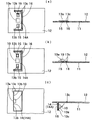
图4的(a)~图4的(d)是示意性表示上述光电混载基板的制造方法中的光波导路单元的制作工序的说明图。FIGS. 4( a ) to 4 ( d ) are explanatory diagrams schematically showing the manufacturing steps of the optical waveguide unit in the method of manufacturing the opto-electric hybrid substrate.
图5的(a)~图5的(c)是示意性表示上述光电混载基板的制造方法中的电路单元的制作工序的说明图。FIGS. 5( a ) to 5 ( c ) are explanatory diagrams schematically showing the steps of manufacturing a circuit unit in the method of manufacturing the opto-electric hybrid board.
图6的(a)~图6的(c)是接着图5示意性表示上述电路单元的制作工序的说明图。6( a ) to 6( c ) are explanatory diagrams schematically showing the manufacturing process of the above-mentioned circuit unit following FIG. 5 .
图7是示意性表示上述光电混载基板的制作工序的说明图。FIG. 7 is an explanatory diagram schematically showing the manufacturing process of the opto-electric hybrid substrate.
图8是示意性表示本发明的光电混载基板的第2实施方式的立体图。Fig. 8 is a perspective view schematically showing a second embodiment of the opto-electric hybrid board of the present invention.
图9的(a)、图9的(b)是示意性表示形成于上述光波导路单元的、电路单元定位用的突起部的变形例的主视图。9( a ) and 9( b ) are front views schematically showing modified examples of protrusions for positioning the circuit unit formed on the optical waveguide unit.
图10的(a)~图10的(d)是示意性表示上述光波导路单元的其他制作工序的说明图。10(a) to 10(d) are explanatory diagrams schematically showing other manufacturing steps of the above-mentioned optical waveguide unit.
图11的(a)~图11的(d)是示意性表示上述光波导路单元的其他方式的制作工序的说明图。FIGS. 11( a ) to 11 ( d ) are explanatory diagrams schematically showing the manufacturing process of another embodiment of the above-mentioned optical waveguide unit.
图12是示意性表示上述光波导路单元的其他方式的立体图。FIG. 12 is a perspective view schematically showing another form of the above-mentioned optical waveguide unit.
图13示意性表示上述光波导路单元的另一其他方式,图13的(a)是其主视图,图13的(b)是图13的(a)的B-B剖视图。FIG. 13 schematically shows another form of the above-mentioned optical waveguide unit, FIG. 13(a) is its front view, and FIG. 13(b) is a B-B sectional view of FIG. 13(a).
图14是示意性表示上述光电混载基板的第3实施方式的剖视图。Fig. 14 is a cross-sectional view schematically showing a third embodiment of the opto-electric hybrid board.
图15是示意性表示以往的光电混载基板的剖视图。Fig. 15 is a cross-sectional view schematically showing a conventional opto-electric hybrid board.
具体实施方式 Detailed ways
接着,根据附图详细说明本发明的实施方式。Next, embodiments of the present invention will be described in detail with reference to the drawings.
图1是示意性表示本发明的光电混载基板的第1实施方式的立体图。该光电混载基板通过分别制作具有电路单元定位用的突起部4的光波导路单元W和具有供该突起部4嵌合的嵌合孔15的电路单元E、并将上述光波导路单元W的上述突起部4嵌合于上述电路单元E的嵌合孔15,使上述光波导路单元W与上述电路单元E相结合而成为一体化。而且,在上述电路单元E中,形成有弯折部14,在该弯折部14形成有上述嵌合孔15,并且安装有光学元件10。在该电路单元E的表面,隔着底座构件S与上述电路单元E呈并列状地载置有上述光波导路单元W。另外,根据需要,也可以隔着上述底座构件S利用粘合剂或粘合带等来固定上述光波导路单元W与上述电路单元E。FIG. 1 is a perspective view schematically showing a first embodiment of an opto-electric hybrid board of the present invention. In this opto-electric hybrid substrate, an optical waveguide unit W having a
在此,在光波导路单元W中,上述突起部4相对于芯2的光透过面(一端面)2a定位形成在规定位置(以在两单元W、E相结合时光波导路单元W的光透过面2a与电路单元E的光学元件10相对的方式预先设定的位置)。另外,在上述电路单元E中,供上述突起部4嵌合的上述嵌合孔15相对于光学元件10定位形成在规定位置(以在两单元W、E相结合时电路单元E的光学元件10与光波导路单元W的光透过面2a相对的方式预先设定的位置)。因此,在上述光电混载基板中,通过上述突起部4与上述嵌合孔15的嵌合,芯2的光透过面2a与光学元件10成为自动地适当地定位、进行了调心的状态。另外,借助于上述底座构件S,光波导路单元被设定在适当的高度位置,并且光电混载基板的强度提高。Here, in the optical waveguide unit W, the
进一步详细说明,上述光波导路单元W的立体图如图2的(a)所示,其A-A剖面的主要部分放大剖视图如图2的(b)所示,上述光波导路单元W具有下包层1、呈规定图案的线状形成于该下包层1的表面的光路用的芯2和以覆盖该芯2的状态形成于上述下包层1的表面的上包层3。而且,在该光波导路单元W的一端缘(在图2的(a)中为左端缘),不存在芯2的、上述下包层1与上包层3的层叠部分沿着芯2的轴向延长,该延长部分形成为电路单元定位用的上述突起部4。该突起部4相对于芯2的光透过面2a定位形成在规定位置。在该实施方式中,上述突起部4配置形成在芯2的两侧(两个位置),上述突起部4的形状形成为厚度(下包层1与上包层3的层叠方向的厚度)恒定、宽度随着朝向延长方向而逐渐变窄的俯视梯形。In further detail, the perspective view of the above-mentioned optical waveguide unit W is shown in (a) of FIG. 1. An
另一方面,上述电路单元E的立体图如图3所示,上述电路单元E具有基板11、形成于该基板11的表面(在图中为下表面)的绝缘层(未图示)、形成于该绝缘层的表面(在图中为下表面)的电路(未图示)和安装于构成该电路单元的局部的光学元件安装用焊盘的光学元件10。而且,在该电路单元E中,上述光学单元10的安装部分相对于上述基板11呈直角地弯折为立起状,形成为长方形板状的弯折部14。该弯折部14是将上述基板11与绝缘层的层叠部分的局部切割为コ字状、将由该コ字状的缺口围成的舌片状部分相对于上述层叠部分呈直角地立起形成的。另外,在该弯折部14形成有供上述光波导路单元W的突起部4(参照图2的(a))嵌合的嵌合孔15。上述弯折部14及上述嵌合孔15相对于上述光学元件10定位形成在规定位置。在该实施方式中,上述嵌合孔15配置形成在上述光学元件10的两侧(两个位置),上述嵌合孔15的形状形成为长方形。On the other hand, the perspective view of the above-mentioned circuit unit E is shown in FIG. A circuit (not shown) on the surface (lower surface in the figure) of this insulating layer and an
另外,上述绝缘层形成于上述基板11中的除了嵌合孔15之外的表面。而且,在该绝缘层的表面,与包括上述光学元件安装用焊盘的电路一起形成有嵌合孔定位用电路(未图示)以及弯折部定位用电路(未图示),该嵌合孔定位用电路作为定位形成上述嵌合孔15时的标记而利用,该弯折部定位用电路作为定位形成上述弯折部14时的标记而利用。上述嵌合孔定位用电路在上述嵌合孔15的周缘形成为框状。上述弯折部定位用电路沿着上述コ字状的缺口而形成,该コ字状的缺口用于形成成为上述弯折部14的上述舌片状部分。而且,在该光学元件安装用焊盘、电路、嵌合孔定位用电路以及弯折部定位用电路的表面形成有镀层(未图示)。在该实施方式中,上述光学元件10采用引线接合型的元件,其发光部或受光部形成于光学元件10的表面(在图3中为右面)In addition, the insulating layer is formed on the surface of the
而且,如图1所示,上述光电混载基板是以上述光波导路单元W的上述突起部4嵌合于上述电路单元E的上述弯折部14的嵌合孔15的状态,使光波导路单元W与电路单元E呈并列状地相结合。在此,如上所述,形成于光波导路单元W的上述突起部4相对于芯2的光透过面2a预先定位形成在规定位置。另外,形成于电路单元E的嵌合孔15相对于光学元件10预先定位形成在规定位置。因此,通过上述突起部4与嵌合孔15的嵌合,芯2的光透过面2a与光学元件10成为适当地定位、自动地进行了调心的状态。而且,上述突起部4与嵌合孔15的嵌合是以光学元件安装部分被弯折的状态(弯折部14)完成,而成为光学元件10与芯2的光透过面2a相对的状态。因此,即使是像本实施方式这样的、与电路单元E呈并列状地设有光波导路单元W的光电混载基板,也无需将芯2的端面形成为光反射用的倾斜面(无需形成为将光路改变90°的构造)。Furthermore, as shown in FIG. 1 , the photoelectric hybrid substrate is in a state where the
而且,在该实施方式中,由于光波导路单元W的上述突起部4形成为梯形,因此通过将电路单元E的上述长方形的嵌合孔15的开口长度设定为规定值,由此能够使上述梯形的突起部4的相对的倾斜面与上述长方形的嵌合孔15的相对的两个面相抵接而适当地设定上述突起部4的嵌合量(嵌合深度),通过该设定,能够适当地设定光波导路单元W的一端面(芯2的光透过面2a)与电路单元E的光学元件10之间的距离。另外,即使上述突起部4的宽度或上述嵌合孔15的开口长度等产生尺寸收缩等,通过利用上述梯形的突起部4的相对的倾斜面,也能够同轴地嵌合上述突起部4与上述嵌合孔15,能够防止芯2与光学元件10的调心偏移。另外,在图1中,为了便于理解,相对于上述突起部4的大小较大地图示了上述嵌合孔15的大小,但是实际上两者的大小相等或上述嵌合孔15的大小稍微大一些。Furthermore, in this embodiment, since the
上述光电混载基板经由下述(1)~(3)的工序制造而成。The opto-electric hybrid substrate is manufactured through the following steps (1) to (3).
(1)制作上述光波导路单元W的工序(参照图4的(a)~图4的(d))。(1) A step of producing the above-mentioned optical waveguide unit W (see FIG. 4( a ) to FIG. 4( d )).
(2)制作上述电路单元E的工序(参照图5的(a)~图5的(c)、图6的(a)~图6的(c))。(2) The process of manufacturing the said circuit unit E (refer FIG. 5(a) - FIG. 5(c), FIG. 6(a) - FIG. 6(c)).
(3)上述光波导路单元W与上述电路单元E相结合的工序(参照图7)。(3) A step of combining the optical waveguide unit W with the electric circuit unit E (see FIG. 7 ).
(1)光波导路单元W的制作工序(1) Manufacturing process of optical waveguide unit W
说明上述(1)的光波导路单元W的制作工序。首先,准备在形成下包层1时所使用的平板状的基座20(参照图4的(a))。作为该基座20的形成材料,例如能够列举出玻璃、石英、硅、树脂、金属等。其中,优选不锈钢制基板。这是因为不锈钢制基板对热的耐伸缩性优异,在上述光波导路单元W的制造过程中,各种尺寸大致维持为设计值。另外,基座20的厚度例如设定在20μm~1mm的范围内。The manufacturing process of the optical waveguide unit W of the above (1) will be described. First, a flat-
接着,如图4的(a)所示,在上述基座20的表面的规定区域,利用光刻法形成在其一端缘的两个位置形成有俯视梯形的突起片1a的下包层1。作为该下包层1的形成材料,使用感光性环氧树脂等感光性树脂。下包层1的厚度例如设定在5μm~50μm的范围内。Next, as shown in FIG. 4( a ), the
接着,如图4的(b)所示,在上述下包层1的表面利用光刻法形成规定图案的芯2。此时,在下包层1的表面中的、上述两个位置的突起片1a之间的部分,将芯2的光透过面(一端面)2a相对于上述两个位置的突起片1a定位在规定位置。该芯2的定位是通过在利用上述光刻法形成芯2时以上述两个位置的突起片1a为基准配置光掩模的状态,隔着上述光掩模曝光而进行的,上述光掩模是以上述两个位置的突起片1a为基准形成的。Next, as shown in FIG. 4( b ),
作为上述芯2的形成材料,例如能够列举出与上述下包层1相同的感光性树脂,上述芯2的形成材料使用折射率比上述下包层1及上包层3(参照图4的(c))的形成材料大的材料。例如能够通过选择上述下包层1、芯2、上包层3的各个形成材料的种类或者调整组成比例来进行该折射率的调整。芯的数量可以是一条也可以是多条(在图4的(b)中为一条)。芯2的图案例如能够列举出直线状、分支状、交叉状等,也可以混和这些直线状、分支状、交叉状等(在图4的(b)中为直线状)的图案。芯2的厚度例如设定在20μm~100μm的范围内。芯2的宽度例如设定在20μm~100μm的范围内。As the forming material of the above-mentioned
然后,如图4的(c)所示,利用光刻法以覆盖上述芯2的方式在上述下包层1的表面形成上包层3。此时,在上述下包层1的突起片1a上也形成与该突起片1a相同形状的突起片3a。作为上述上包层3的形成材料,例如能够列举出与上述下包层1相同的感光性树脂。上述上包层3的厚度(距下包层1的表面的厚度)例如设定在超过芯2的厚度且1000μm以下的范围内。Then, as shown in FIG. 4( c ), the
在此,上述下包层1的突起片1a与形成在其上的上述上包层3的突起片3a的层叠部分成为电路单元定位用的上述突起部4。而且,如上所述,芯2的光透过面2a相对于上述下包层1的突起片1a定位形成在规定位置,因此在该突起片1a层叠上述上包层的突起片3a而成的上述突起部4相对于芯2的光透过面2a定位形成在规定位置。上述突起部4的尺寸例如分别设定为突出量在300μm~5000μm的范围内、宽度在100μm~5000μm的范围内。Here, the lamination portion of the protruding
接着,如图4的(d)所示,从下包层1的背面剥离基座20(参照图4的(c))。这样,获得了光波导路单元W,该光波导路单元W具有下包层1、芯2以及上包层3,并在上述下包层1与上包层3的层叠部分延伸设置有电路单元定位用的突起部4。该光波导路单元W的厚度例如设定在30μm~1150μm的范围内。这样,上述(1)的光波导路单元W的制作工序完成。Next, as shown in FIG. 4( d ), the
(2)电路单元E的制作工序(2) Manufacturing process of circuit unit E
接着,使用图5的(a)~图5的(c)、图6的(a)~图6的(c)说明上述(2)的电路单元E的制作工序。在该图5的(a)~图5的(c)、图6的(a)~图6的(c)的各图中,左右示出了两个图,左侧的图是俯视图,右侧的图是沿中心线的纵剖视图。Next, the manufacturing process of the circuit unit E of said (2) is demonstrated using FIG.5(a) - FIG.5(c), FIG.6(a) - FIG.6(c). In each of Fig. 5 (a) to Fig. 5 (c) and Fig. 6 (a) to Fig. 6 (c), two diagrams are shown on the left and right, the diagram on the left is a plan view, and the diagram on the right is a plan view. The side figure is a longitudinal sectional view along the center line.
首先,准备上述基板11(参照图5的(a))。作为该基板11的形成材料,例示能够列举出金属、树脂等。其中,基于易加工性及尺寸稳定性的观点,优选不锈钢制基板。另外,上述基板11的厚度例如设定在0.02mm~0.1mm的范围内。First, the above-mentioned
接着,如图5的(a)所示,在上述基板11的表面的规定区域形成绝缘层12。该绝缘层12的形成例如是在涂布了由感光性聚酰亚胺树脂等绝缘层形成用的感光性树脂溶解于溶剂中而获得的清漆之后,根据需要对该清漆的涂布层进行加热处理而使其干燥,形成绝缘层形成用的感光性树脂层。然后,利用紫外线等辐射线隔着光掩模对该感光性树脂层进行曝光,从而形成规定形状的绝缘层12。绝缘层12的厚度例如设定在5μm~15μm的范围内。Next, as shown in FIG. 5( a ), an insulating
接着,如图5的(b)所示,在上述绝缘层12的表面同时形成包括光学元件安装用焊盘13a的电路(未图示)、框状的嵌合孔定位用电路13b以及コ字状的弯折部定位用电路13c,制作电路基板。这些电路等的形成例如利用半添加法来进行。Next, as shown in FIG. 5 (b), on the surface of the above-mentioned insulating
即,首先,在上述绝缘层12的表面,通过溅射或非电解电镀等形成金属层(厚度60nm~260nm左右)。该金属层成为进行后面的电解电镀时的晶种层(成为形成电解电镀层的基底的层)。接着,在由上述基板11、绝缘层12及晶种层构成的层叠体的两面粘贴干膜抗蚀剂,之后在形成有上述晶种层一侧的干膜抗蚀剂,利用光刻法同时形成上述电路等的图案的孔部,在该孔部的底部暴露上述晶种层的表面部分。接着,通过电解电镀,在暴露于上述孔部的底部的上述晶种层的表面部分层叠形成电解电镀层(厚度5μm~20μm左右)。然后,利用氢氧化钠水溶液等剥离上述干膜抗蚀剂。之后,通过软蚀刻去除未形成有上述电解电镀层的晶种层部分,将由剩余的电解电镀层及该剩余的电解电镀层的下面的晶种层构成的层叠部分形成为上述电路等。这样,获得了由上述基板11、绝缘层12、包括光学元件安装用焊盘13a的电路、嵌合孔定位用电路13b及弯折部定位用电路13c构成的电路基板。That is, first, a metal layer (about 60 nm to 260 nm in thickness) is formed on the surface of the insulating
然后,将该电路基板安装于曝光机,利用相机拍摄表面侧(电路侧)与背面侧(基板11侧),根据该图像,以上述表面侧的框状的嵌合孔定位用电路13b为标记,适当地定位上述背面侧的嵌合孔预定形成部(上述框状的嵌合孔定位用电路13b在框内相对应的部分)的位置,并且以上述表面侧的弯折部定位用电路13c为标记,适当地定位弯折部预定形成部(舌片状部分14A)在背面侧的位置。接着,利用干膜抗蚀剂(未图示)覆盖该背面侧的、除了用于形成上述嵌合孔预定形成部及舌片状的上述弯折部预定形成部的コ字状的预定切割部以外的部分。接着,如图5的(c)所示,使用氯化铁水溶液进行蚀刻来去除所暴露的上述嵌合孔预定形成部及上述コ字状的预定切割部的基板11的部分。由此,从该去除部分11a、11b暴露出上述绝缘层12的部分。Then, this circuit board is installed in an exposure machine, and the front side (circuit side) and the back side (
接着,如图6的(a)所示,使用化学蚀刻液进行蚀刻来去除上述暴露的绝缘层12的部分。由此,将上述嵌合孔预定形成部形成为嵌合孔15,并且将上述コ字状的预定切割部形成为コ字状的缺口16(设为コ字状的贯通状态)。上述嵌合孔15及コ字状的缺口16以利用上述半添加法与光学元件安装用焊盘13a同时形成的框状的嵌合孔定位用电路13b及弯折部定位用电路13c为基准而形成,因此上述嵌合孔15及コ字状的缺口16相对于上述光学元件安装用焊盘13a定位形成在规定位置。上述嵌合孔15的开口长度及开口宽度设定为与嵌合于该嵌合孔15的上述光波导路单元的突起部4(参照图1)的嵌合部分的宽度及厚度相同或者比其稍微(例如1μm~100μm左右)大。Next, as shown in (a) of FIG. 6 , etching is performed using a chemical etchant to remove the exposed portion of the insulating
接着,通过实施电解电镀处理,在包括上述光学元件安装用焊盘13a的电路、嵌合孔定位用电路13b及弯折部定位用电路13c的表面形成镀层(未图示)。之后,利用氢氧化钠水溶液等剥离上述干膜抗蚀剂。另外,作为上述镀层的成分,能够列举出金、镍等。另外,该镀层的厚度通常设定在0.2μm~0.5μm的范围内。Next, electrolytic plating is performed to form a plating layer (not shown) on the surfaces of the circuit including the optical
然后,如图6的(b)所示,在光学元件安装用焊盘13a的表面,隔着上述镀层安装上述光学元件10。之后,根据需要,树脂密封(未图示)上述光学元件10及其周边部。Then, as shown in FIG. 6( b ), the
然后,如图6的(c)所示,与上述电路基板呈直角地将由上述コ字状的缺口16(参照图6的(b))所围成的、安装有上述光学元件10的舌片状部分14A弯折为下垂状,并形成为弯折部14。即,上述光学元件10安装在该弯折部14的规定位置。这样,获得了具有上述嵌合孔15及上述弯折部14的电路单元E。在此,如上所述,在图6的(a)的工序中形成的上述嵌合孔15相对于上述光学元件安装用焊盘13a定位形成在规定位置,因此安装于该光学元件安装用焊盘13a的光学元件10与上述嵌合孔15成为相互进行了定位的位置关系。这样,上述(2)的电路单元E的制作工序完成。Then, as shown in FIG. 6(c), the tongue on which the above-mentioned
(3)光波导路单元W与电路单元E的结合工序(3) Bonding process of optical waveguide unit W and circuit unit E
接着,说明光波导路单元W与电路单元E的结合工序。如图7(上下颠倒地图示了图6(c)所示的电路单元E)的立体图所示,该结合是,以上述电路单元E的弯折部14的光学元件10与上述光波导路单元W的芯2的光透过面2a相面对的状态,使上述光波导路单元W的突起部4嵌合于上述弯折部14的嵌合孔15,使上述光波导路单元W与上述电路单元E一体化。之后,根据需要,利用粘合剂固定上述突起部4与嵌合孔15的嵌合部。然后,在上述电路单元E的表面,隔着底座构件S(参照图1)载置上述光波导路单元W。之后,根据需要,也可以隔着上述底座构件S利用粘合剂或粘合带等来固定上述光波导路单元W与上述电路单元E。这样,上述(3)的光波导路单元W与电路单元E的结合工序完成,完成了作为目标的光电混载基板。Next, a coupling process of the optical waveguide unit W and the circuit unit E will be described. As shown in the perspective view of FIG. 7 (showing the circuit unit E shown in FIG. 6(c) upside down), the combination is that the
在此,如上所述,在上述光波导路单元W中,芯2的光透过面2a与电路单元定位用的突起部4成为相互进行了定位的位置关系。另外,在安装有上述光学元件10的电路单元E中,光学元件10与供上述突起部4嵌合的嵌合孔15成为相互进行了定位的位置关系。因此,如上所述,通过使上述突起部4嵌合于上述嵌合孔15而制作上述光电混载基板时,芯2的光透过面2a与光学元件10自动地进行调心。其结果,在上述光电混载基板的制作中,不需要进行费时费力的调心作业。即,上述光电混载基板的量产性优异。Here, as described above, in the optical waveguide unit W, the
而且,上述光波导路单元W的突起部4是用于构成该光波导路单元W的下包层1及上包层3的规定部分延伸设置而成的。另外,上述电路单元E的嵌合孔15形成在构成该电路单元E的电路基板。即,在上述突起部4与上述嵌合孔15的嵌合中未设置连接器等其他部件。因此,在光波导路单元W与电路单元E的结合中不存在上述连接器等其他部件所造成的尺寸误差、位置偏移的累积,因此光波导路单元W的芯2与电路单元E的光学元件10的调心为高精度。另外,上述突起部4与上述嵌合孔15的嵌合不需要连接器等其他部件,因此也不需要管理该连接器等的尺寸精度,根据这一点,量产性也优异。Furthermore, the
而且,上述突起部4与嵌合孔15的嵌合以光学元件安装部分被弯折的状态(弯折部14)完成而成为光学元件10与芯2的光透过面2a相对的状态。因此,即使是像本实施方式这样的、与电路单元E呈并列状地设置光波导路单元W的光电混载基板的制造方法,也无需将芯2的端面形成为光反射用的倾斜面(无需形成为将光路改变90°的构造)。Furthermore, the fitting of the
另外,在上述实施方式中,通常,光学元件10的大小大于光波导路单元W的厚度,因此如上所述,在安装有光学元件10的弯折部14中,在芯2的光透过面2a与光学元件10进行了调心的状态下,在电路单元E与光波导路单元W之间形成有间隙。上述底座构件S是为了填充该间隙、即、为了调整光波导路单元W相对于电路单元E的高度而设置的。In addition, in the above-mentioned embodiment, the size of the
图8是示意性表示本发明的光电混载基板的第2实施方式的立体图。在该实施方式中,如图所示,电路单元E的弯折部14是通过利用4条平行的弯折线17a~17d弯折而形成的。因此,在相邻的弯折线17a~17d之间形成有三个位置的平板部分18A~18C。而且,在这三个位置的平板部分18A~18C中的、中间的平板部分18B的规定位置,与上述第1实施方式相同地安装有光学元件10,并且形成有供光波导路单元W的突起部4嵌合的嵌合孔15。该中间的平板部分18B相对于电路单元E的基板11呈直角。Fig. 8 is a perspective view schematically showing a second embodiment of the opto-electric hybrid board of the present invention. In this embodiment, as shown in the drawing, the
在该第2实施方式中,上述弯折线17a~17d相对于光学元件10定位形成在规定的位置。而且,通过弯折这些弯折线17a~17d来形成上述弯折部14,能够将电路单元E中的、光波导路单元W的载置面的高度位置设定在规定的高度位置。因此,光波导路单元W的突起部4与电路单元E的嵌合孔15相嵌合,在芯2的光透过面2a与光学元件10进行了调心的状态下,能够使得在电路单元E与光波导路单元W之间不形成间隙。因此,在该第2实施方式中,不设置在上述第1实施方式中设置的底座构件S(参照图1)。除此以外的电路单元E的部分及光波导路单元W皆与图1所示的上述第1实施方式相同,对相同的部分标注相同的附图标记。而且,起到了与上述第1实施方式相同的作用、效果。In the second embodiment, the bending lines 17 a to 17 d are formed at predetermined positions with respect to the
在该第2实施方式中,在对电路单元E的基板11进行蚀刻的工序(参照图5的(c))中,用于形成电路单元E的弯折部14的上述规定的弯折线17a~17d通过对上述基板11进行半蚀刻而形成在以光学元件安装用焊盘13a为基准的规定位置。In this second embodiment, in the step of etching the
图9的(a)、图9的(b)是示意性表示上述电路单元定位用的突起部4的变形例的主视图。即,在图9的(a)中,上述突起部4形成为三角形。该情况与图1所示的梯形的突起部4相同,利用三角形的倾斜面能够适当地设定光波导路单元W的一端面(芯2的光透过面2a)与电路单元E的光学元件10之间的距离,而且,也能够防止芯2与光学元件10的调心偏移(参照图1)。在图9的(b)中,上述突起部4形成为台阶状。在该情况下,在上述突起部4嵌合于嵌合孔15(参照图1)后,突起部4不易脱落。除了上述以外,例如也可以将上述突起部4形成为半圆状等。FIG. 9( a ) and FIG. 9( b ) are front views schematically showing a modified example of the
图10的(a)~图10的(d)示意性示出了在光波导路单元W的制作中作为包括突起片3a的上包层3(参照图4的(c))的其他制作工序(制作方法)的模具成形的方法。即,在上述各个实施方式中,利用光刻法形成了包括上述突起片3a的上包层3,但是也可以通过模具成形方法形成。该形成如下进行。FIGS. 10( a ) to 10 ( d ) schematically show other manufacturing steps of the upper cladding layer 3 (see FIG. 4( c )) including the protruding
即,首先,如图10的(a)所示,准备在其上表面形成有凹部的成形模具30,该凹部具有与包括上述突起片3a的上包层3的形状相对应的模具面31。接着,如图10的(b)所示(与图4的(b)相同),在基座20的表面形成具有突起片1a的下包层1,在该下包层1的表面以规定图案形成芯2。然后,如图10的(c)所示,在上述成形模具30的凹部填满上包层形成用的树脂,之后以上述芯2浸入该树脂内的方式(上下颠倒地表示图10的(b)所示的图)使基座20的表面与上述成形模具30的上表面紧密接触。此时,将上述成形模具30的、与上述突起片3a对应的模具面部分31a定位在下包层1的突起片1a上。接着,在该树脂为感光性树脂的情况下,透过上述成形模具30用紫外线等辐射线进行曝光,之后进行加热处理,在上述树脂为热固化树脂的情况下,进行加热处理。由此,上述上包层形成用的树脂固化,形成了包括上述突起片3a的上包层3。然后,进行脱模,如图10的(d)所示(上下颠倒地图示了从图10的(c)所图示的状态脱模了的图),获得与图4的(c)相同的构件。也可以如下地形成。That is, first, as shown in FIG. 10( a ), a
图11的(a)~图11的(d)示意性示出了光波导路单元W的其他方式的制作工序。即,在上述各个实施方式中,将光波导路单元W中的电路单元定位用的突起部4设为了延伸设置下包层1与上包层3的层叠部分而成的部分(参照图4的(c)),但是也可以设为仅延伸设置了上包层3而成的部分。这种光波导路单元W的制作工序(制作方法)以如下方法进行。FIG. 11( a ) to FIG. 11( d ) schematically show the manufacturing steps of other forms of the optical waveguide unit W. As shown in FIG. That is, in each of the above-described embodiments, the
即,首先,如图11的(a)所示,在基座20的表面的规定区域,利用光刻法形成没有上述突起片1a(参照图4的(a))的下包层1。接着,如图11的(b)所示,在上述下包层1的表面利用光刻法形成规定图案的芯2。接着,如图11的(c)所示,准备在其上表面形成有凹部的成形模具30,该凹部具有与包括突起部4的上包层3的形状相对应的模具面31。然后,如图11的(d)所示,在上述成形模具30的凹部填满上包层形成用的树脂,之后以上述芯2浸入该树脂内的方式使基座20的表面与上述成形模具30的上表面紧密接触。此时,将上述成形模具30的、与上述突起部4对应的模具面部分31a相对于芯2的光透过面2a进行定位。之后,与图10的(c)所说明的上述方法相同地形成包括上述突起部4的上包层3。然后,进行脱模,如图12所示,获得了在基座20的表面仅在上包层3延伸设置有上述突起部4的光波导路单元W。或者,取代上述模具成形方法(参照图11的(c)~图11的(d)),也可以利用光刻法来进行上述上包层3的形成。That is, first, as shown in FIG. 11( a ), the under
另外,在上述实施方式(参照图11的(a)~图11的(d))中,仅在上包层3延伸设置了电路单元定位用的突起部4,但是也可以仅在下包层1延伸设置电路单元定位用的突起部4。这种光波导路单元W的制作工序(制作方法)能够通过如下的方法进行制作,即,在基座20的表面形成具有突起片1a的下包层1,在该下包层1的表面以规定图案形成了芯2的状态(与图4的(b)相同的状态)下,通过模具成形方法或光刻法来形成没有上述突起片3a(参照图4的(c))的上包层3。In addition, in the above-mentioned embodiment (see FIG. 11( a ) to FIG. 11( d )), the
图13的(a)、图13的(b)示意性示出了光波导路单元W的另一其他实施方式。在该实施方式中,如图13的(a)的主视图、图13的(b)的图13的(a)的B-B剖视图所示,上包层3形成为比下包层1大一圈。这种光波导路单元W也可以利用如上所述的模具成形方法或光刻法来制作。(a) and (b) of FIG. 13 schematically show another embodiment of the optical waveguide unit W. As shown in FIG. In this embodiment, as shown in the front view of FIG. 13(a) and the B-B sectional view of FIG. 13(a) in FIG. 13(b), the
如上所述(参照图10的(a)~图10的(c)、图11的(a)~图11的(d)、图13的(a)、图13的(b)),当通过模具成形方法形成电路单元定位用的突起部4时,能够将该突起部4的厚度形成得较厚,在将该突起部4嵌合于电路单元E的嵌合孔15的状态下,能够增强该嵌合部分的强度。另外,在上述模具成形时,通过使上述成形模具30的、与上述突起部4相对应的模具面部分31a变形,也可以将上述突起部4的厚度形成为随着朝向延长方向逐渐变薄。As described above (refer to FIG. 10 (a) to FIG. 10 (c), FIG. 11 (a) to FIG. 11 (d), FIG. 13 (a), FIG. When the protruding
另外,在上述实施方式中,作为光学元件10采用了引线接合型的元件,但是也可以采用倒装芯片型的元件。在采用该倒装芯片型的元件的情况下,由于发光部或受光部形成于光学元件10的安装面(背面),因此如图14所示,光波导路单元W从未安装有光学元件10的一侧与电路单元E相嵌合,在电路单元E的与上述发光部或受光部相对应的部分形成有光通过用的贯通孔19。In addition, in the above-described embodiment, a wire bonding type element is used as the
另外,在上述各个实施方式中,说明了光电混载基板的一端部,另一端部也可以形成为与上述各个实施方式的一端部相同的结构。在该情况下,作为上述光学元件10,例如在一端部侧安装发光元件,在另一端部侧安装受光元件,从而能够用上述受光元件通过芯2接收来自该发光元件的光。In addition, in each of the above-mentioned embodiments, one end of the photoelectric hybrid board has been described, but the other end may have the same structure as that of the one end of each of the above-mentioned embodiments. In this case, as the
而且,在上述各个实施方式中,在电路单元E的制作工序中,在电路、光学元件安装用焊盘13a、嵌合孔定位用电路13b以及弯折部定位用电路13c的表面形成了镀层,但是该镀层是根据需要形成的,在不需要时,也可以不形成镀层。In addition, in each of the above-mentioned embodiments, in the production process of the circuit unit E, plating is formed on the surfaces of the circuit, the optical
接着,说明实施例。但是,本发明并不限定于实施例。Next, examples will be described. However, this invention is not limited to an Example.
实施例Example
下包层、上包层的形成材料Materials for forming the lower cladding layer and the upper cladding layer
成分A:含有脂环骨架的环氧树脂(大赛璐化学工业公司制、EHPE3150)100质量份。Component A: 100 parts by mass of an alicyclic skeleton-containing epoxy resin (manufactured by Daicel Chemical Industries, Ltd., EHPE3150).
成分B:光产酸剂(San-Apro公司制、CPI-200K)2质量份。Component B: 2 parts by mass of a photoacid generator (manufactured by San-Apro, CPI-200K).
将这些成分A、B溶解于环己酮中,调制出下包层及上包层的形成材料(感光性树脂)。These components A and B were dissolved in cyclohexanone to prepare a material (photosensitive resin) for forming the lower cladding layer and the upper cladding layer.
芯的形成材料core forming material
成分C:邻甲酚酚醛清漆缩水甘油醚(O-cresol novolacglycidylether)(新日铁化学制、YDCN-700-10)100质量份。Component C: 100 parts by mass of o-cresol novolac glycidylether (manufactured by Nippon Steel Chemical Co., Ltd., YDCN-700-10).
将该成分C与1质量份的上述成分B溶解乳酸乙脂中,调制出芯的形成材料(感光性树脂)。This component C and 1 part by mass of the above-mentioned component B were dissolved in ethyl lactate to prepare a core forming material (photosensitive resin).
实施例1Example 1
光波导路单元的制作Fabrication of Optical Waveguide Units
使用上述下包层、芯、上包层的各个形成材料,以与上述第1实施方式(参照图2的(a)、图2的(b))相同的方法制作出具有电路单元定位用的等腰梯形的突起部的光波导路单元。上述等腰梯形的突起部的尺寸设为底边(长边)的宽度为2.5mm,顶边(短边)的宽度为1.0mm,高度(突出长度)为3.0mm,相邻的突起部的中心之间的距离为6.5mm。Using the above-mentioned materials for forming the under clad layer, core, and over clad layer, a circuit unit positioning circuit board is produced in the same manner as in the above-mentioned first embodiment (see FIG. 2(a) and FIG. 2(b)). An optical waveguide unit with an isosceles trapezoidal protrusion. The size of the protrusion of the above-mentioned isosceles trapezoid is set as the width of the base (long side) to be 2.5 mm, the width of the top side (short side) to be 1.0 mm, and the height (protrusion length) to be 3.0 mm. The distance between centers is 6.5mm.
电路单元的制作Fabrication of circuit units
以与上述第1实施方式(参照图3)相同的方法制作出电路单元,该电路单元在弯折部安装有光学元件、并且形成有供上述电路单元定位用的突起部嵌合的长方形的嵌合孔。该嵌合孔的尺寸设为开口长度为2.5mm,开口宽度为0.1mm,相邻的嵌合孔的中心之间的距离为6.5mm。另外,作为光学元件,安装了引线接合型的发光元件(ULM Photonics公司制、ULM850-10-CO0104U)。In the same manner as in the above-mentioned first embodiment (see FIG. 3 ), a circuit unit is manufactured, the circuit unit is mounted with an optical element at the bent portion, and a rectangular fitting is formed for fitting the protrusion for positioning the above-mentioned circuit unit. Hole. The dimensions of the fitting holes were 2.5 mm in opening length, 0.1 mm in opening width, and 6.5 mm in the distance between the centers of adjacent fitting holes. In addition, as an optical element, a wire bonding type light emitting element (ULM850-10-CO0104U manufactured by ULM Photonics Co., Ltd.) was mounted.
光电混载基板的制造Manufacture of photoelectric hybrid substrate
将上述光波导路单元的突起部嵌合于上述电路单元的嵌合孔,而使上述光波导路单元与上述电路单元一体化。然后,利用粘合剂固定其嵌合部。另外,在上述光波导路单元与上述电路单元之间设置底座构件。The protruding portion of the optical waveguide unit is fitted into the fitting hole of the circuit unit to integrate the optical waveguide unit and the circuit unit. Then, the fitting portion is fixed with an adhesive. In addition, a base member is provided between the optical waveguide unit and the electric circuit unit.
光传播试验light propagation test
向上述实施例1的光电混载基板的发光元件中通电,使光从发光元件出射。然后,确认到光从光电混载基板的芯的另一端部出射。Electricity was supplied to the light-emitting element of the photoelectric hybrid substrate of the above-mentioned Example 1, and light was emitted from the light-emitting element. Then, it was confirmed that light was emitted from the other end portion of the core of the opto-electric hybrid substrate.
实施例2Example 2
光波导路单元的制作Fabrication of Optical Waveguide Units
在上述实施例1的光波导路单元的基础上,制成另一端部也与一端部相同地具有电路单元定位用的等腰梯形的突起部的光波导路单元。除此以外皆与上述实施例1相同。In addition to the optical waveguide unit of Example 1 above, an optical waveguide unit having an isosceles trapezoidal protrusion for positioning a circuit unit at the other end similarly to the one end was produced. Other than that, it is the same as the above-mentioned Example 1.
电路单元的制作Fabrication of circuit units
制作与上述实施例1相同的电路单元。而且,在上述实施例1的电路单元中,制成取代发光元件而安装了引线接合型的受光元件(albis公司制、PDCA04-70-GS)的电路单元。The same circuit unit as in
光电混载基板的制造Manufacture of photoelectric hybrid substrate
与上述实施例1相同地在上述光波导路单元的一端部固定安装有上述发光元件的电路单元,在另一端部固定安装有上述受光元件的电路单元。In the same manner as in the first embodiment, the circuit unit of the light-emitting element is fixed to one end of the optical waveguide unit, and the circuit unit of the light-receiving element is fixed to the other end.
信号传输试验Signal transmission test
向上述实施例2的光电混载基板的发光元件中通电,使光从发光元件出射。然后,确认到该光被受光元件接收。Electricity was supplied to the light-emitting element of the photoelectric hybrid substrate of the above-mentioned Example 2, and light was emitted from the light-emitting element. Then, it was confirmed that the light was received by the light receiving element.
根据上述实施例1、2的结果可知,在上述制造方法中,即使不进行光波导路单元的芯与电路单元的光学元件(发光元件、受光元件)的调心作业,所获得的光电混载基板也适当地进行光传播。From the results of Examples 1 and 2 above, it can be seen that in the above-mentioned manufacturing method, even if the alignment operation between the core of the optical waveguide unit and the optical elements (light-emitting element, light-receiving element) of the circuit unit is not performed, the obtained photoelectric hybrid The substrate is also suitable for light propagation.
另外,如上述第2实施方式(参照图8)、图9~图14所示,在所形成的光电混载基板中,与上述实施例1、2相同地也能够获得即使不进行调心作业也能适当地进行光传播这样的结果。In addition, as shown in the above-mentioned second embodiment (see FIG. 8 ) and FIGS. 9 to 14 , in the formed opto-electric hybrid board, similar to the above-mentioned Examples 1 and 2, even if no alignment operation is performed, it is possible to obtain As a result, light propagation can also be properly performed.
产业上的可利用性Industrial availability
本发明的光电混载基板能够用于以高速传送或者处理声音、图像等数字信号的信息通信设备、信号处理装置等。The photoelectric hybrid board of the present invention can be used for information communication equipment, signal processing devices, etc. that transmit or process digital signals such as voice and image at high speed.
附图标记说明Explanation of reference signs
W、光波导路单元;E、电路单元;2、芯;2a、光透过面;4、突起部;10、光学元件;14、弯折部;15、嵌合孔。W, optical waveguide unit; E, circuit unit; 2, core; 2a, light transmission surface; 4, protruding part; 10, optical element; 14, bending part; 15, fitting hole.
Claims (4)
Applications Claiming Priority (2)
| Application Number | Priority Date | Filing Date | Title |
|---|---|---|---|
| JP2011-073618 | 2011-03-29 | ||
| JP2011073618A JP5608125B2 (en) | 2011-03-29 | 2011-03-29 | Opto-electric hybrid board and manufacturing method thereof |
Publications (2)
| Publication Number | Publication Date |
|---|---|
| CN102736193A true CN102736193A (en) | 2012-10-17 |
| CN102736193B CN102736193B (en) | 2015-03-04 |
Family
ID=46927360
Family Applications (1)
| Application Number | Title | Priority Date | Filing Date |
|---|---|---|---|
| CN201210055272.2A Expired - Fee Related CN102736193B (en) | 2011-03-29 | 2012-03-05 | Opto-electric hybrid board and manufacturing method therefor |
Country Status (3)
| Country | Link |
|---|---|
| US (1) | US8837873B2 (en) |
| JP (1) | JP5608125B2 (en) |
| CN (1) | CN102736193B (en) |
Cited By (1)
| Publication number | Priority date | Publication date | Assignee | Title |
|---|---|---|---|---|
| TWI866040B (en) * | 2022-01-31 | 2024-12-11 | 日商京瓷股份有限公司 | Optical circuit substrate and optical parts mounting structure |
Families Citing this family (9)
| Publication number | Priority date | Publication date | Assignee | Title |
|---|---|---|---|---|
| JP5351096B2 (en) * | 2010-06-02 | 2013-11-27 | 日東電工株式会社 | Optical waveguide manufacturing method |
| JP5351102B2 (en) | 2010-07-05 | 2013-11-27 | 日東電工株式会社 | Optical waveguide manufacturing method |
| JP5351101B2 (en) | 2010-07-05 | 2013-11-27 | 日東電工株式会社 | Optical waveguide manufacturing method |
| JP5379774B2 (en) | 2010-10-27 | 2013-12-25 | 日東電工株式会社 | Optical waveguide manufacturing method |
| JP5608125B2 (en) * | 2011-03-29 | 2014-10-15 | 日東電工株式会社 | Opto-electric hybrid board and manufacturing method thereof |
| US20140086533A1 (en) * | 2012-09-27 | 2014-03-27 | Ezra GOLD | Method for alignment between two optical components |
| KR101925476B1 (en) * | 2015-11-25 | 2018-12-05 | 주식회사 옵텔라 | optical module and optical engine having the same |
| JP2018124394A (en) * | 2017-01-31 | 2018-08-09 | 国立大学法人福井大学 | Light beam projection device |
| US11635186B2 (en) * | 2018-03-13 | 2023-04-25 | Motherson Innovations Company Limited | Polymeric substrate and a method of providing same |
Citations (4)
| Publication number | Priority date | Publication date | Assignee | Title |
|---|---|---|---|---|
| US20090097802A1 (en) * | 2007-10-16 | 2009-04-16 | Sumitomo Electric Industries, Ltd. | Optical module and method for making the same |
| JP4631671B2 (en) * | 2005-11-29 | 2011-02-16 | オムロン株式会社 | Optical cable module and electronic device including optical cable module |
| CN101988975A (en) * | 2009-08-03 | 2011-03-23 | 日东电工株式会社 | Manufacturing method of optical sensor module and optical sensor module obtained thereby |
| US20110216995A1 (en) * | 2010-03-05 | 2011-09-08 | Nitto Denko Corporation | Method of manufacturing optical sensor module and optical sensor module obtained thereby |
Family Cites Families (22)
| Publication number | Priority date | Publication date | Assignee | Title |
|---|---|---|---|---|
| JPH05196831A (en) | 1992-01-22 | 1993-08-06 | Fujitsu Ltd | Automatic alignment device and automatic alignment method |
| US5265184A (en) * | 1992-05-28 | 1993-11-23 | Motorola, Inc. | Molded waveguide and method for making same |
| US5249245A (en) * | 1992-08-31 | 1993-09-28 | Motorola, Inc. | Optoelectroinc mount including flexible substrate and method for making same |
| US5625734A (en) * | 1995-05-31 | 1997-04-29 | Motorola | Optoelectronic interconnect device and method of making |
| US5768456A (en) * | 1996-11-22 | 1998-06-16 | Motorola, Inc. | Optoelectronic package including photonic device mounted in flexible substrate |
| EP1122567A1 (en) * | 2000-02-02 | 2001-08-08 | Corning Incorporated | Passive alignement using slanted wall pedestal |
| JP2002250846A (en) * | 2001-02-26 | 2002-09-06 | Seiko Epson Corp | Optical module, manufacturing method thereof, and optical transmission device |
| JP3807385B2 (en) * | 2003-05-14 | 2006-08-09 | セイコーエプソン株式会社 | OPTICAL MODULE AND ITS MANUFACTURING METHOD, OPTICAL COMMUNICATION DEVICE, ELECTRONIC DEVICE |
| JP3794489B2 (en) * | 2003-06-18 | 2006-07-05 | セイコーエプソン株式会社 | OPTICAL COMMUNICATION MODULE AND METHOD FOR MANUFACTURING THE SAME, OPTICAL COMMUNICATION DEVICE, AND ELECTRONIC DEVICE |
| TWI230810B (en) * | 2004-01-30 | 2005-04-11 | Ind Tech Res Inst | Opto-electronic transmission module and fabrication method thereof |
| CN100492079C (en) * | 2004-06-09 | 2009-05-27 | 日本电气株式会社 | Optical waveguide module |
| JPWO2008096716A1 (en) * | 2007-02-05 | 2010-05-20 | 日本電信電話株式会社 | Semiconductor submodule, method of connecting connector and semiconductor submodule, and optical module |
| JP5156502B2 (en) * | 2007-06-26 | 2013-03-06 | パナソニック株式会社 | Optical module |
| US7720337B2 (en) * | 2007-12-20 | 2010-05-18 | Intel Corporation | Wafer based optical interconnect |
| JP5263286B2 (en) * | 2008-03-11 | 2013-08-14 | 富士通オプティカルコンポーネンツ株式会社 | Connection device and optical device |
| JP5223050B2 (en) | 2008-03-17 | 2013-06-26 | 独立行政法人産業技術総合研究所 | Optical module |
| JP2010192883A (en) | 2009-01-20 | 2010-09-02 | Sumitomo Bakelite Co Ltd | Optical and electric combined substrate and method of manufacturing optical and electric combined substrate |
| JP5271141B2 (en) * | 2009-04-06 | 2013-08-21 | 日東電工株式会社 | Manufacturing method of opto-electric hybrid module and opto-electric hybrid module obtained thereby |
| JP5674516B2 (en) * | 2011-03-14 | 2015-02-25 | 日東電工株式会社 | Opto-electric hybrid board and manufacturing method thereof |
| JP5608122B2 (en) * | 2011-03-28 | 2014-10-15 | 日東電工株式会社 | Opto-electric hybrid board and manufacturing method thereof |
| JP5674525B2 (en) * | 2011-03-29 | 2015-02-25 | 日東電工株式会社 | Manufacturing method of opto-electric hybrid board |
| JP5608125B2 (en) * | 2011-03-29 | 2014-10-15 | 日東電工株式会社 | Opto-electric hybrid board and manufacturing method thereof |
-
2011
- 2011-03-29 JP JP2011073618A patent/JP5608125B2/en not_active Expired - Fee Related
-
2012
- 2012-03-05 CN CN201210055272.2A patent/CN102736193B/en not_active Expired - Fee Related
- 2012-03-07 US US13/413,853 patent/US8837873B2/en not_active Expired - Fee Related
Patent Citations (4)
| Publication number | Priority date | Publication date | Assignee | Title |
|---|---|---|---|---|
| JP4631671B2 (en) * | 2005-11-29 | 2011-02-16 | オムロン株式会社 | Optical cable module and electronic device including optical cable module |
| US20090097802A1 (en) * | 2007-10-16 | 2009-04-16 | Sumitomo Electric Industries, Ltd. | Optical module and method for making the same |
| CN101988975A (en) * | 2009-08-03 | 2011-03-23 | 日东电工株式会社 | Manufacturing method of optical sensor module and optical sensor module obtained thereby |
| US20110216995A1 (en) * | 2010-03-05 | 2011-09-08 | Nitto Denko Corporation | Method of manufacturing optical sensor module and optical sensor module obtained thereby |
Cited By (1)
| Publication number | Priority date | Publication date | Assignee | Title |
|---|---|---|---|---|
| TWI866040B (en) * | 2022-01-31 | 2024-12-11 | 日商京瓷股份有限公司 | Optical circuit substrate and optical parts mounting structure |
Also Published As
| Publication number | Publication date |
|---|---|
| US20120251038A1 (en) | 2012-10-04 |
| JP5608125B2 (en) | 2014-10-15 |
| JP2012208305A (en) | 2012-10-25 |
| US8837873B2 (en) | 2014-09-16 |
| CN102736193B (en) | 2015-03-04 |
Similar Documents
| Publication | Publication Date | Title |
|---|---|---|
| CN102736193B (en) | Opto-electric hybrid board and manufacturing method therefor | |
| CN102681106B (en) | Optical/electrical mixed mounting substrate and manufacture method thereof | |
| US8915657B2 (en) | Opto-electric hybrid board and manufacturing method therefor | |
| JP5271141B2 (en) | Manufacturing method of opto-electric hybrid module and opto-electric hybrid module obtained thereby | |
| CN101988975B (en) | Manufacturing method of optical sensor module and optical sensor module obtained thereby | |
| JP5693986B2 (en) | Optical sensor module | |
| CN101726794A (en) | Manufacturing method of opto-electric hybrid module and opto-electric hybrid module obtained by the method | |
| KR20110101059A (en) | Method for manufacturing optical sensor module and optical sensor module obtained by the same | |
| CN102043199A (en) | Method of manufacturing optical sensor module and optical sensor module obtained thereby | |
| CN102346046B (en) | Optical sensor module | |
| CN102681107B (en) | Opto-electric hybrid board and manufacturing method therefor | |
| CN102385108B (en) | Optical sensor module | |
| CN104919345B (en) | Opto-electric hybrid module | |
| CN102707393B (en) | Opto-electric hybrid board and manufacturing method therefor | |
| CN102736192B (en) | Optical/electrical mixed mounting substrate and manufacture method thereof | |
| JP2012234025A (en) | Opto-electric hybrid substrate and manufacturing method of the same |
Legal Events
| Date | Code | Title | Description |
|---|---|---|---|
| C06 | Publication | ||
| PB01 | Publication | ||
| C10 | Entry into substantive examination | ||
| SE01 | Entry into force of request for substantive examination | ||
| C14 | Grant of patent or utility model | ||
| GR01 | Patent grant | ||
| CF01 | Termination of patent right due to non-payment of annual fee |
Granted publication date: 20150304 Termination date: 20170305 |
|
| CF01 | Termination of patent right due to non-payment of annual fee |