CN102473820A - LED with silicone layer and laminated remote phosphor layer - Google Patents
LED with silicone layer and laminated remote phosphor layer Download PDFInfo
- Publication number
- CN102473820A CN102473820A CN2010800350575A CN201080035057A CN102473820A CN 102473820 A CN102473820 A CN 102473820A CN 2010800350575 A CN2010800350575 A CN 2010800350575A CN 201080035057 A CN201080035057 A CN 201080035057A CN 102473820 A CN102473820 A CN 102473820A
- Authority
- CN
- China
- Prior art keywords
- layer
- phosphor
- silicone
- phosphor layer
- led
- Prior art date
- Legal status (The legal status is an assumption and is not a legal conclusion. Google has not performed a legal analysis and makes no representation as to the accuracy of the status listed.)
- Pending
Links
Images


Classifications
-
- H—ELECTRICITY
- H10—SEMICONDUCTOR DEVICES; ELECTRIC SOLID-STATE DEVICES NOT OTHERWISE PROVIDED FOR
- H10H—INORGANIC LIGHT-EMITTING SEMICONDUCTOR DEVICES HAVING POTENTIAL BARRIERS
- H10H20/00—Individual inorganic light-emitting semiconductor devices having potential barriers, e.g. light-emitting diodes [LED]
- H10H20/80—Constructional details
- H10H20/85—Packages
- H10H20/851—Wavelength conversion means
- H10H20/8515—Wavelength conversion means not being in contact with the bodies
-
- H—ELECTRICITY
- H10—SEMICONDUCTOR DEVICES; ELECTRIC SOLID-STATE DEVICES NOT OTHERWISE PROVIDED FOR
- H10H—INORGANIC LIGHT-EMITTING SEMICONDUCTOR DEVICES HAVING POTENTIAL BARRIERS
- H10H20/00—Individual inorganic light-emitting semiconductor devices having potential barriers, e.g. light-emitting diodes [LED]
- H10H20/80—Constructional details
- H10H20/85—Packages
- H10H20/855—Optical field-shaping means, e.g. lenses
-
- H—ELECTRICITY
- H10—SEMICONDUCTOR DEVICES; ELECTRIC SOLID-STATE DEVICES NOT OTHERWISE PROVIDED FOR
- H10H—INORGANIC LIGHT-EMITTING SEMICONDUCTOR DEVICES HAVING POTENTIAL BARRIERS
- H10H20/00—Individual inorganic light-emitting semiconductor devices having potential barriers, e.g. light-emitting diodes [LED]
- H10H20/01—Manufacture or treatment
- H10H20/036—Manufacture or treatment of packages
- H10H20/0361—Manufacture or treatment of packages of wavelength conversion means
-
- H—ELECTRICITY
- H10—SEMICONDUCTOR DEVICES; ELECTRIC SOLID-STATE DEVICES NOT OTHERWISE PROVIDED FOR
- H10H—INORGANIC LIGHT-EMITTING SEMICONDUCTOR DEVICES HAVING POTENTIAL BARRIERS
- H10H20/00—Individual inorganic light-emitting semiconductor devices having potential barriers, e.g. light-emitting diodes [LED]
- H10H20/80—Constructional details
- H10H20/84—Coatings, e.g. passivation layers or antireflective coatings
-
- H—ELECTRICITY
- H10—SEMICONDUCTOR DEVICES; ELECTRIC SOLID-STATE DEVICES NOT OTHERWISE PROVIDED FOR
- H10H—INORGANIC LIGHT-EMITTING SEMICONDUCTOR DEVICES HAVING POTENTIAL BARRIERS
- H10H20/00—Individual inorganic light-emitting semiconductor devices having potential barriers, e.g. light-emitting diodes [LED]
- H10H20/80—Constructional details
- H10H20/85—Packages
- H10H20/8506—Containers
-
- H—ELECTRICITY
- H10—SEMICONDUCTOR DEVICES; ELECTRIC SOLID-STATE DEVICES NOT OTHERWISE PROVIDED FOR
- H10H—INORGANIC LIGHT-EMITTING SEMICONDUCTOR DEVICES HAVING POTENTIAL BARRIERS
- H10H20/00—Individual inorganic light-emitting semiconductor devices having potential barriers, e.g. light-emitting diodes [LED]
- H10H20/80—Constructional details
- H10H20/85—Packages
- H10H20/852—Encapsulations
- H10H20/853—Encapsulations characterised by their shape
-
- H—ELECTRICITY
- H10—SEMICONDUCTOR DEVICES; ELECTRIC SOLID-STATE DEVICES NOT OTHERWISE PROVIDED FOR
- H10W—GENERIC PACKAGES, INTERCONNECTIONS, CONNECTORS OR OTHER CONSTRUCTIONAL DETAILS OF DEVICES COVERED BY CLASS H10
- H10W72/00—Interconnections or connectors in packages
- H10W72/071—Connecting or disconnecting
- H10W72/072—Connecting or disconnecting of bump connectors
- H10W72/07251—Connecting or disconnecting of bump connectors characterised by changes in properties of the bump connectors during connecting
-
- H—ELECTRICITY
- H10—SEMICONDUCTOR DEVICES; ELECTRIC SOLID-STATE DEVICES NOT OTHERWISE PROVIDED FOR
- H10W—GENERIC PACKAGES, INTERCONNECTIONS, CONNECTORS OR OTHER CONSTRUCTIONAL DETAILS OF DEVICES COVERED BY CLASS H10
- H10W72/00—Interconnections or connectors in packages
- H10W72/20—Bump connectors, e.g. solder bumps or copper pillars; Dummy bumps; Thermal bumps
Landscapes
- Led Device Packages (AREA)
Abstract
A method for making a light emitting device is described in which an array of flip chip Light Emitting Diode (LED) dies is mounted on a submount wafer. A hemispherical first silicone layer is simultaneously molded over each LED die. A preformed flexible phosphor layer comprising phosphor powder soaked in silicone is laminated over the first silicone layer to conform to the outer surface of the hemispherical first silicone layer. A silicone lens is then molded over the phosphor layer. By prefabricating the phosphor layer, the phosphor layer can be made to very tight tolerances and tested. By molding the hemispherical silicone layer to separate the phosphor layer from the LED die, the color versus viewing angle relationship is constant and the phosphor is not degraded by heat. The flexible phosphor layer may include a plurality of different phosphor layers and may include a reflector or other layers.
Description
Technical field
Thereby the present invention relates to have the overlying strata wavelength Conversion LED emitting light emitting diode (LED) of phosphor, and particularly relate in LED laminated remote phosphor to realize the technology of more accurately color control and more uniform color and visual angle relation.
Background technology
Prior art Fig. 1 explains the conventional flip chip LED tube core 10 on the part that is installed in submount wafer 12.In flip-chip, n contacts on the same side that all is formed at the LED tube core with p.
Can disclose the other details of finding LED among US2006/0281203Al and the 2005/0269582Al at assignee's United States Patent(USP) No. 6,649,440 and 6,274,399 and United States Patent (USP), all these are incorporated into this by reference.
In order to use blue led tube core 10 to produce white light; Be well known that through for example spray or the spin coating adhesive in phosphor, electrophoresis, in reflector, use phosphor or other means; Directly above tube core 10, deposit YAG phosphor, perhaps redness and green phosphor.It is also known that, the prefabricated tile of phosphor (for example, the phosphor powder of sintering) is attached to the top of LED tube core 10.This phosphor layer is not long-range, because the surface of their direct contact semiconductor tube cores 10.Blue light and the combination of phosphor light revealed through phosphor produce white light.The problem of this non-remote phosphors comprises: 1) for high-capacity LED, photon density is very high and make phosphor saturated; 2) the very hot and phosphor of LED can react and causes phosphor particles to be embedded in polymeric binder layer (for example, silicones) deepening wherein heat; 3) owing to pass the different angles (normal direction blue ray pass minimum thickness) of blue ray of the phosphor of different-thickness, color is with visual angle change; And 4) be difficult to form phosphor layer thickness and density very uniformly.
Also known with phosphor powder be immersed in the silicon resin adhesive and with silicone molded above the LED tube core to form lens.Yet the mould tolerance influences the thickness and the alignment of phosphor, and this influences integral color and color and visual angle relation.The mould tolerance is generally the 30-50 micron, and the phosphor thickness of expectation only is about 100 microns, therefore for White LED on a certain visual angle of client's appointment, be difficult to realize+/-50K target correlated colour temperature (CCT).
The blue led tube core that uses same process to form produces different slightly main wavelength, and LED sorts according to their main wavelength sometimes.Therefore if the same phosphor layer is applied to each blue led tube core, then for the LED tube core of each letter sorting batch, whole colour temperature will be different.If White LED need be mated, backlight such as being used for, this LED must be from same letter sorting batch.For some harsh application, in fact this reduced productive rate.
In addition, use prior art processes, the reproducibility of phosphor layer is difficult.
Need a kind of technology that does not suffer the formation phosphor-converted LED of above-mentioned defective.
Summary of the invention
In order to realize that more accurately phosphor layer has used remote phosphor to be used to form white light (or another color) with blueness or UV LED tube core.Remote phosphor is separated with the LED tube core, therefore compares the lower and phosphor experience lower temperature of photon density with the phosphor that directly is formed on the LED die surfaces.Photon density is lower, because before being incident upon on the remote phosphor, the LED die light is launched on than large tracts of land.
In order to realize accuracy bigger in phosphor layer thickness, density and the wavelength conversion characteristics, phosphor layer is by prefabricated, and the layer of test comprises the phosphor powder that is immersed in the silicon resin adhesive.The plate of this phosphor layer forms thickness and the phosphor density with strict control.This plate is to be tested, such as through using blue light to encourage it, exports to confirm its main wavelength.Phosphor plate with different qualities is mated with the blue led tube core that sorts subsequently.In this way, can use from the blue led of difference letter sorting batch and realize target white light CCT.
For prefabricated phosphor layer and LED tube core are separated, silicone layer at first is molded on the LED tube core with package die.In one embodiment, this first molded silicone layer has hemispherical shape basically.The phosphor plate of coupling is utilized vacuum laminated on silicone layer, and application of heat is attached to silicone layer with phosphor plate.Any typical inaccuracy (for example, the 30-50 micron) when forming silicone layer in mould or the alignment does not influence white light CCT significantly, at this moment because phosphor layer long-range and will also have hemispherical shape.
Second silicone layer is molded on the phosphor layer with the protection phosphor layer and as lens.In one embodiment, second silicone layer is hemisphere basically, makes White LED output lambert figure.Thereby the shape of second silicone lens can be formed the emission figure that produces any kind.
LED die array to being installed on the submount wafer is carried out above process simultaneously.Die array can be from single letter sorting batch.Phosphor layer can be the single plate that strides across entire wafer.Wafer subsequently by unification to tell white light LEDs/pedestal.
In one embodiment, phosphor layer contains YAG phosphor (yellow-green).In another embodiment, phosphor layer contains the redness and the green phosphor of mixing.In another embodiment, phosphor layer comprises a plurality of layer, such as the layer of redness and the YAG layer that separates with the generation warm white.This technology can be used to use the phosphor of any type to make any color of light.
Description of drawings
Fig. 1 is prior art blueness or the cross sectional view of UV flip-chip LED tube core that is installed on the pedestal.
Fig. 2 explanation is covered with the LED die array, and such as the simplification submount wafer of 500-4000 LED, wherein all the LED tube cores on the wafer are handled simultaneously.
Fig. 3 explains submount wafer, and it is made as against mould to be used to form first silicone layer that is used for the packaged LED tube core and phosphor layer and LED tube core are separated.
Fig. 4 explains the LED tube core in the mould recess that is immersed in the silicones filling.
That Fig. 5 explains is prefabricated, thin and flexible phosphor layer, and it uses vacuum and heat to be layered on the molded silicone layer, makes phosphor layer be adapted to the outer surface of silicone layer.
Fig. 6 explanation has the phosphor plate of red phosphor layer and YAG phosphor (or green phosphor) layer.
Fig. 7 explains the cascade phosphor plate, and wherein top layer forms and has lenticule.
Fig. 8 explains the cascade phosphor plate, wherein on the bottom, has the reflector, but this reflector is through blue light reflection Red, green and sodium yellow.
Fig. 9 explains the cascade phosphor plate, and wherein top surface forms and has the characteristic of variable thickness with coupling individual LED tube core.
On having, Figure 10 explanation covers the phosphor layer of uvea (pigmented layer).
The white light LEDs of Figure 11 explanation after carrying out technology described herein.
The wafer that Figure 12 explanation removes from mould after solidifying.
Figure 13 explains that submount wafer is by the LED of unification with formation individual LED/pedestal.
Use same numbers mark element identical or of equal value.
Embodiment
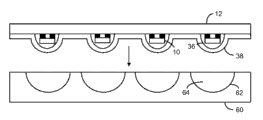
Fig. 2 is the simplified illustration of submount wafer 12, and LED die array 10 is installed on this submount wafer 12.Can have 500-4000 LED on the single submount wafer 12.All LED on the wafer 12 will use following method to handle simultaneously.
Be described below, first silicone layer is molded on the LED tube core 10 with package die 10.
Fig. 3 explanation is positioned at submount wafer 12 and the part of LED tube core 10 on the mould 30, and this mould 30 has with liquid silicone 34, or the cavity 32 of softening silicones 34 or powder silicones 34 or the filling of tablet silicones.If silicones 34 is not with liquid or softening form dispensing, then mould 30 is heated with softening silicones 34.Submount wafer 12 is made as mould 30 against, and is as shown in Figure 4, makes LED tube core 10 be immersed in the silicones 34 in each cavity 32.Wafer 12 is pressed together to force silicones 34 to fill all cavities with mould 30.The periphery sealing allows high pressure, when silicones 34 filling cavities, allows all air to escape simultaneously.Also can around sealing, use vacuum source and between wafer 12 and mould 30, spur the formation vacuum.
The type that depends on employed silicones 34, mould 30 is heated with solidification of silicon resin 34 subsequently.If original silicones 34 is solid (for example, powder or tablet) in room temperature, then mould 30 is cooled so that silicones 34 sclerosis.Replacedly, can use transparent mould and can use UV photocuring silicones 34.
The type that depends on employed silicones 34, wafer 12 can pass through the back curing temperature of about 25OoC subsequently, thereby additionally makes silicone layer 36 sclerosis.Can use the material beyond the silicones, such as epoxy molding mixture or another suitable polymers of powder type.
Also can use injection moulding to form silicone layer 36, wherein wafer 12 is located at together with mould, and liquid silicone utilizes pressure injection in mould through inlet, and forms vacuum.Passage aisle between the cavity body of mould allows silicones to fill all cavitys.Silicones solidifies through heating subsequently, and mould and wafer were opened in 12 minutes.
Such as hereinafter description, silicone layer 36 is used for even phosphor layer and LED tube core are separated.
Fig. 5 explanation is laminated to the surface of wafer 12 and the prefabricated phosphor layer 38 of silicone layer 36.Phosphor layer 38 can have same size with wafer 12.Phosphor layer 38 is formed by suitable phosphor powder, such as YAG, and redness or green phosphor, perhaps any combination of phosphor, thus realize the color of object emission.In order to form phosphor layer 38, phosphor powder is mixed with silicones realizing target density, and phosphor layer 38 forms and has target thickness.Through this mixture being spin-coated on the flat surfaces or molded phosphor layer the thickness that can obtain to expect.
After phosphor layer 38 solidifies,, can test phosphor layer 38 through using blue-light source excitation phosphor layer 38 and measuring light emission.Because blue led is the different slightly main wavelength of emission usually, blue led can be to be tested before being installed on the submount wafer 12, and LED is sorted according to their main wavelength.The prefabricated phosphor layer of variable thickness or phosphor density subsequently with LED coupling from specific letter sorting batch, the color emission that obtains can all be identical target white (or CCT).If all the LED tube cores on the submount wafer 12 are from matching that letter sorting batch before same letter sorting batch and the phosphor layer 38, then color emission will be target CCT.
In one embodiment, phosphor layer 38 thickness are about hundreds of micron and very soft.
As shown in Figure 5, the phosphor layer 38 of coupling places on the wafer 12, thereby and between phosphor layer 38 and wafer 12, vacuumizes and remove all air.This is silicon-coated resin bed 36 and wafer 12 conformally.Thereby this structure is heated subsequently the silicones in the phosphor layer 38 is attached to silicone layer 36.
Through range upon range of prefabricated phosphor layer rather than form phosphor on the LED tube core, evenly phosphor thickness and density are guaranteed.Be very easy to form even phosphor plate.Through using silicone layer 36 phosphor layer 38 and LED tube core were opened in 10 minutes; The photon density at phosphor layer 38 places reduces; The hot degenerate problem that does not have phosphor; The refractive index of silicone layer 36 can be adjusted with the increase extraction efficiency, and does not have the mould tolerance that influences phosphor layer 38 performances.Owing to there not being the unjustified phosphor layer that influences of mould, so color homogeneity improves.Color is consistent with the visual angle relation, because blue LED light is at the phosphor layer 38 of all angles through same thickness.
Another advantage of prefabricated range upon range of phosphor layer 38 is that phosphor layer can form customization of each layer quilt and accurately formation by a plurality of layers.Fig. 6-10 explanation can be layered in some the cascade phosphor layers on the wafer 12.In a preferred embodiment, owing to easily each is stacked layer by layer, prefabricated laminated plate, and plate is to be tested and be laminated to wafer 12 as single flaggy subsequently.Replacedly, a plurality of layers can be layered on the wafer 12 individually.
On having, Fig. 6 explanation covers the red phosphor layer 40 of YAG phosphor layer 42.Red phosphor layer 40 is customized to form warm white, because yellow-green YAG phosphor is tending towards forming dazzling white.Substitute YAG, can use green phosphor.The phosphor layer that can form arbitrary number is to form the desired color characteristic.In one embodiment, one of them is blue phosphor layer to use UV LED tube core and said layer.A plurality of phosphor layers can separately form and use heat and pressure and/or vacuum laminated being in the same place.
Fig. 7 explains that top phosphor layer 44 can be molded to have micro lens (or other optical element) in its surface, perhaps realizes increasing light scattering or other optical effect thereby reduce TIR.
Fig. 8 explains range upon range of layer, and one of them can be a color reflectors 46, and it allows blue light through still reflecting more long wavelength's light.In this way, the light that is produced by phosphor is not absorbed by LED tube core 10, and always is reflected upwards.
Fig. 9 explains that top phosphor layer 48 can be molded having different-thickness, thus with wafer 12 on independent blue led tube core 10 couplings, thereby realize same target CCT for each LED.
Figure 10 explains that phosphor layer 42 can be range upon range of with non-phosphor optical layers 50, and this non-phosphor optical layers can be that painted colour filter, light scattering layer (for example, contain TiO
2The silicones of particle) or the layer of other type.
Figure 11 explains wafer 12, and mould 60 forms silicone lens on LED thereby range upon range of phosphor layer 38 is made as against.The refractive index through adjusting silicones and the shape of lens, this will protect range upon range of phosphor layer 38, form any desired emission figure and increase light extraction.
In Figure 11, mould 60 contains useful silicones 64 and fills to be used to form the cavity 62 of hemispherical lens 66 (Figure 12).Molding process can be said identical with combination Fig. 3.Lens 66 can be the lens of surface launching lens or any other type on the contrary.Can even have phosphor powder (for example, red-emitting phosphor) in the lens 66 with skew output colour temperature.
The wafer 12 that removes from mould 60 after Figure 12 is illustrated in and solidifies.
In one embodiment, first silicone layer 38 has 1.4 refractive index, and lens 66 have 1.5 refractive index to reduce by the percentage of the blue photons of internal reflection.The mould that is used for outer lens 66 can form roughened outer surface to increase light extraction efficiency.
Through using the range upon range of of prefabricated phosphor layer 38, the mould tolerance does not influence color emission or color and visual angle relation.Because the many LED from identical letter sorting batch are handled simultaneously on wafer scale, and phosphor layer 38 as big plate by range upon range of, LED generates target CCT with very tight tolerance (less than 50K), and handles relatively easy.
In this disclosure; Term " submount wafer " is intended to represent to be used for the support of LED die array; Wherein electrically contacting on the wafer is attached to the electrode on the LED tube core; And wafer subsequently by unification to form the one or more LED on the single pedestal, wherein pedestal has the electrode that is connected to power supply.
Although illustrated and described specific embodiment of the present invention; It will be apparent to those skilled in the art that; On more broad range of the present invention, can change and adjust and do not deviate from the present invention, so all this change and adjustment that accompanying claims will be in its encompasses drops on true spirit of the present invention and scope.
Claims (15)
Applications Claiming Priority (3)
| Application Number | Priority Date | Filing Date | Title |
|---|---|---|---|
| US12/537909 | 2009-08-07 | ||
| US12/537,909 US20110031516A1 (en) | 2009-08-07 | 2009-08-07 | Led with silicone layer and laminated remote phosphor layer |
| PCT/IB2010/053113 WO2011015959A1 (en) | 2009-08-07 | 2010-07-07 | Led with silicone layer and laminated remote phosphor layer |
Publications (1)
| Publication Number | Publication Date |
|---|---|
| CN102473820A true CN102473820A (en) | 2012-05-23 |
Family
ID=43017061
Family Applications (1)
| Application Number | Title | Priority Date | Filing Date |
|---|---|---|---|
| CN2010800350575A Pending CN102473820A (en) | 2009-08-07 | 2010-07-07 | LED with silicone layer and laminated remote phosphor layer |
Country Status (9)
| Country | Link |
|---|---|
| US (1) | US20110031516A1 (en) |
| EP (1) | EP2462634A1 (en) |
| JP (1) | JP2013501372A (en) |
| KR (1) | KR20120056843A (en) |
| CN (1) | CN102473820A (en) |
| BR (1) | BR112012002431A2 (en) |
| RU (1) | RU2012108576A (en) |
| TW (1) | TW201123549A (en) |
| WO (1) | WO2011015959A1 (en) |
Cited By (5)
| Publication number | Priority date | Publication date | Assignee | Title |
|---|---|---|---|---|
| CN104485411A (en) * | 2014-11-14 | 2015-04-01 | 江苏脉锐光电科技有限公司 | A remote phosphor lens and manufacturing method and application thereof |
| CN106885194A (en) * | 2015-12-15 | 2017-06-23 | 现代自动车株式会社 | Light source module and use its headlight for vehicle |
| CN111052422A (en) * | 2017-09-01 | 2020-04-21 | 科锐公司 | Light emitting diodes, components and related methods |
| CN113490887A (en) * | 2018-12-21 | 2021-10-08 | 亮锐控股有限公司 | Photoresist patterning process supporting two-step phosphor deposition to form LED matrix array |
| CN115411023A (en) * | 2022-08-22 | 2022-11-29 | 深圳市未林森科技有限公司 | COB light source color uniformity control process method with small error |
Families Citing this family (99)
| Publication number | Priority date | Publication date | Assignee | Title |
|---|---|---|---|---|
| US8525207B2 (en) * | 2008-09-16 | 2013-09-03 | Osram Sylvania Inc. | LED package using phosphor containing elements and light source containing same |
| US8912023B2 (en) * | 2009-04-08 | 2014-12-16 | Ledengin, Inc. | Method and system for forming LED light emitters |
| US8323748B2 (en) * | 2009-05-15 | 2012-12-04 | Achrolux Inc. | Methods for forming uniform particle layers of phosphor material on a surface |
| WO2010151600A1 (en) | 2009-06-27 | 2010-12-29 | Michael Tischler | High efficiency leds and led lamps |
| JP5379615B2 (en) * | 2009-09-09 | 2013-12-25 | パナソニック株式会社 | Lighting device |
| JP2011082339A (en) * | 2009-10-07 | 2011-04-21 | Nitto Denko Corp | Kit for optical semiconductor encapsulation |
| US8653539B2 (en) | 2010-01-04 | 2014-02-18 | Cooledge Lighting, Inc. | Failure mitigation in arrays of light-emitting devices |
| US9480133B2 (en) | 2010-01-04 | 2016-10-25 | Cooledge Lighting Inc. | Light-emitting element repair in array-based lighting devices |
| US8384121B2 (en) | 2010-06-29 | 2013-02-26 | Cooledge Lighting Inc. | Electronic devices with yielding substrates |
| US8771577B2 (en) * | 2010-02-16 | 2014-07-08 | Koninklijke Philips N.V. | Light emitting device with molded wavelength converting layer |
| US8901586B2 (en) * | 2010-07-12 | 2014-12-02 | Samsung Electronics Co., Ltd. | Light emitting device and method of manufacturing the same |
| US20120081000A1 (en) * | 2010-10-05 | 2012-04-05 | Power Data Communications Co., Ltd. | Led encapsulation process and shield structure made thereby |
| TWI445216B (en) * | 2010-11-17 | 2014-07-11 | 宏齊科技股份有限公司 | Light-emitting diode package structure with deposition type fluorescent coating layer and manufacturing method thereof |
| DE102011013369A1 (en) * | 2010-12-30 | 2012-07-05 | Osram Opto Semiconductors Gmbh | A method of manufacturing a plurality of semiconductor devices |
| TWI441361B (en) * | 2010-12-31 | 2014-06-11 | 英特明光能股份有限公司 | Light-emitting diode package structure and manufacturing method thereof |
| WO2012100132A1 (en) * | 2011-01-21 | 2012-07-26 | Osram Sylvania Inc. | Luminescent converter and led light source containing same |
| US8941137B2 (en) * | 2011-03-06 | 2015-01-27 | Mordehai MARGALIT | Light emitting diode package and method of manufacture |
| EP2689458B8 (en) * | 2011-03-25 | 2018-08-29 | Lumileds Holding B.V. | Patterned uv sensitive silicone-phosphor layer over leds, and method for fabricating the same |
| KR20120119350A (en) * | 2011-04-21 | 2012-10-31 | 삼성전자주식회사 | Light emitting device module and method for manufacturing the same |
| US9029887B2 (en) | 2011-04-22 | 2015-05-12 | Micron Technology, Inc. | Solid state lighting devices having improved color uniformity and associated methods |
| DE102011102350A1 (en) * | 2011-05-24 | 2012-11-29 | Osram Opto Semiconductors Gmbh | Optical element, optoelectronic component and method for the production of these |
| US8480267B2 (en) | 2011-06-28 | 2013-07-09 | Osram Sylvania Inc. | LED lighting apparatus, systems and methods of manufacture |
| US8585243B2 (en) | 2011-06-28 | 2013-11-19 | Osram Sylvania Inc. | LED lighting apparatus, systems and methods of manufacture |
| WO2013008157A1 (en) | 2011-07-14 | 2013-01-17 | Koninklijke Philips Electronics N.V. | Method of manufacturing a phosphor-enhanced light source |
| KR101294415B1 (en) | 2011-07-20 | 2013-08-08 | 엘지이노텍 주식회사 | Optical member and display device having the same |
| CN102270730A (en) * | 2011-07-27 | 2011-12-07 | 晶科电子(广州)有限公司 | LED (light emitting diode) device free of gold wires |
| US8952402B2 (en) | 2011-08-26 | 2015-02-10 | Micron Technology, Inc. | Solid-state radiation transducer devices having flip-chip mounted solid-state radiation transducers and associated systems and methods |
| US8579451B2 (en) | 2011-09-15 | 2013-11-12 | Osram Sylvania Inc. | LED lamp |
| US9349927B2 (en) * | 2011-10-18 | 2016-05-24 | Nitto Denko Corporation | Encapsulating sheet and optical semiconductor element device |
| US9444024B2 (en) * | 2011-11-10 | 2016-09-13 | Cree, Inc. | Methods of forming optical conversion material caps |
| US10043960B2 (en) * | 2011-11-15 | 2018-08-07 | Cree, Inc. | Light emitting diode (LED) packages and related methods |
| JP2013135084A (en) * | 2011-12-26 | 2013-07-08 | Nitto Denko Corp | Light-emitting diode device manufacturing method |
| RU2617880C2 (en) | 2012-02-10 | 2017-04-28 | Конинклейке Филипс Н.В. | Moulded lens forming led-module of integrated circuit scale and manufacturing method thereof |
| US8591076B2 (en) | 2012-03-02 | 2013-11-26 | Osram Sylvania Inc. | Phosphor sheet having tunable color temperature |
| US9388959B2 (en) * | 2012-03-02 | 2016-07-12 | Osram Sylvania Inc. | White-light emitter having a molded phosphor sheet and method of making same |
| JP5912712B2 (en) * | 2012-03-21 | 2016-04-27 | スタンレー電気株式会社 | Optical system for illumination |
| KR102228997B1 (en) | 2012-03-29 | 2021-03-18 | 루미리즈 홀딩 비.브이. | Phosphor in inorganic binder for led applications |
| WO2013144919A1 (en) | 2012-03-29 | 2013-10-03 | Koninklijke Philips N.V. | Phosphor in inorganic binder for led applications |
| US20130279194A1 (en) * | 2012-04-22 | 2013-10-24 | Liteideas, Llc | Light emitting systems and related methods |
| CN103378260A (en) * | 2012-04-24 | 2013-10-30 | 展晶科技(深圳)有限公司 | Method for manufacturing packaging structure of light emitting diode |
| US8877561B2 (en) | 2012-06-07 | 2014-11-04 | Cooledge Lighting Inc. | Methods of fabricating wafer-level flip chip device packages |
| CN104471730B (en) | 2012-07-20 | 2018-04-17 | 皇家飞利浦有限公司 | Light emitting device and method of creating light emitting device |
| JP6024957B2 (en) * | 2012-09-24 | 2016-11-16 | 東芝ライテック株式会社 | Light emitting device and lighting device |
| EP2917938B1 (en) | 2012-11-07 | 2020-05-06 | Lumileds Holding B.V. | Wavelength converted light emitting device |
| US9543478B2 (en) | 2012-11-07 | 2017-01-10 | Koninklijke Philips N.V. | Light emitting device including a filter and a protective layer |
| CN103022325B (en) * | 2012-12-24 | 2016-01-20 | 佛山市香港科技大学Led-Fpd工程技术研究开发中心 | The LED encapsulation structure of application long distance formula phosphor powder layer and method for making thereof |
| US10439107B2 (en) * | 2013-02-05 | 2019-10-08 | Cree, Inc. | Chip with integrated phosphor |
| KR101319360B1 (en) * | 2013-03-04 | 2013-10-16 | 유버 주식회사 | Chip on board type uv led package and method for making the same |
| US8876312B2 (en) * | 2013-03-05 | 2014-11-04 | Avago Technologies General Ip (Singapore) Pte. Ltd. | Lighting device and apparatus with spectral converter within a casing |
| US8928219B2 (en) | 2013-03-05 | 2015-01-06 | Avago Technologies General Ip (Singapore) Pte. Ltd. | Lighting device with spectral converter |
| US9470395B2 (en) | 2013-03-15 | 2016-10-18 | Abl Ip Holding Llc | Optic for a light source |
| US10400984B2 (en) | 2013-03-15 | 2019-09-03 | Cree, Inc. | LED light fixture and unitary optic member therefor |
| TWI527274B (en) * | 2013-04-29 | 2016-03-21 | 新世紀光電股份有限公司 | Light emitting diode package structure |
| KR20150025231A (en) * | 2013-08-28 | 2015-03-10 | 서울반도체 주식회사 | Light source module and manufacturing method thereof, backlight unit |
| US20150226385A1 (en) * | 2014-02-11 | 2015-08-13 | Cree, Inc. | Systems and Methods for Application of Coatings Including Thixotropic Agents onto Optical Elements, and Optical Elements Having Coatings Including Thixotropic Agents |
| US9680067B2 (en) | 2014-03-18 | 2017-06-13 | GE Lighting Solutions, LLC | Heavily phosphor loaded LED packages having higher stability |
| US9590148B2 (en) | 2014-03-18 | 2017-03-07 | GE Lighting Solutions, LLC | Encapsulant modification in heavily phosphor loaded LED packages for improved stability |
| DE102014106074A1 (en) * | 2014-04-30 | 2015-11-19 | Osram Opto Semiconductors Gmbh | Lighting device and method for producing a lighting device |
| CN105098025A (en) * | 2014-05-07 | 2015-11-25 | 新世纪光电股份有限公司 | Light emitting device |
| JP6077670B2 (en) * | 2014-05-09 | 2017-02-08 | 富士高分子工業株式会社 | Phosphor-containing identification object and method for manufacturing the same |
| KR101641205B1 (en) * | 2014-05-12 | 2016-07-21 | 주식회사 케이케이디씨 | The manufacturing method for LED light module contained adjustable Emitting angle |
| US9997676B2 (en) | 2014-05-14 | 2018-06-12 | Genesis Photonics Inc. | Light emitting device and manufacturing method thereof |
| TWI557952B (en) | 2014-06-12 | 2016-11-11 | 新世紀光電股份有限公司 | Light-emitting element |
| TWI641285B (en) | 2014-07-14 | 2018-11-11 | 新世紀光電股份有限公司 | Light-emitting module and light-emitting unit manufacturing method |
| TWI631733B (en) * | 2014-10-09 | 2018-08-01 | 新世紀光電股份有限公司 | Light emitting device |
| TWI583025B (en) * | 2014-10-09 | 2017-05-11 | 新世紀光電股份有限公司 | Thin-film flip-chip light emitting diode having dual sub-mounts and method for manufacturing the same |
| US9755110B1 (en) | 2016-07-27 | 2017-09-05 | Sharp Laboratories Of America, Inc. | Substrate with topological features for steering fluidic assembly LED disks |
| US9985190B2 (en) | 2016-05-18 | 2018-05-29 | eLux Inc. | Formation and structure of post enhanced diodes for orientation control |
| US9917226B1 (en) | 2016-09-15 | 2018-03-13 | Sharp Kabushiki Kaisha | Substrate features for enhanced fluidic assembly of electronic devices |
| US10249599B2 (en) | 2016-06-29 | 2019-04-02 | eLux, Inc. | Laminated printed color conversion phosphor sheets |
| US9892944B2 (en) | 2016-06-23 | 2018-02-13 | Sharp Kabushiki Kaisha | Diodes offering asymmetric stability during fluidic assembly |
| DE102015001723A1 (en) | 2015-02-05 | 2016-08-11 | Sergey Dyukin | The method of improving the characteristics of lighting devices with a front lighting of the light guide, which include the luminophore, which is illuminated with semiconductor structures. |
| DE102015103835A1 (en) * | 2015-03-16 | 2016-09-22 | Osram Opto Semiconductors Gmbh | Light-emitting component and method for producing a light-emitting component |
| US10984735B2 (en) * | 2015-04-17 | 2021-04-20 | Nanosys, Inc. | White point uniformity in display devices |
| US10217914B2 (en) * | 2015-05-27 | 2019-02-26 | Samsung Electronics Co., Ltd. | Semiconductor light emitting device |
| CN106469772B (en) * | 2015-08-18 | 2018-01-05 | 江苏诚睿达光电有限公司 | A kind of process of the thermoplastic resin light conversion body fitting encapsulation LED based on rolling-type |
| US10816165B2 (en) | 2015-11-19 | 2020-10-27 | Lsi Industries, Inc. | LED luminaire assembly |
| USD781482S1 (en) | 2015-12-28 | 2017-03-14 | Lsi Industries, Inc. | Luminaire |
| EP3205584B1 (en) * | 2016-02-12 | 2020-06-03 | Goodrich Lighting Systems GmbH | Exterior aircraft light and aircraft comprising the same |
| US9627437B1 (en) | 2016-06-30 | 2017-04-18 | Sharp Laboratories Of America, Inc. | Patterned phosphors in through hole via (THV) glass |
| EP3491679B1 (en) | 2016-07-26 | 2023-02-22 | CreeLED, Inc. | Light emitting diodes, components and related methods |
| DE102016115533A1 (en) * | 2016-08-22 | 2018-02-22 | Osram Opto Semiconductors Gmbh | Optoelectronic semiconductor chip, method for producing an optoelectronic semiconductor chip and headlight with an optoelectronic semiconductor chip |
| US10243097B2 (en) | 2016-09-09 | 2019-03-26 | eLux Inc. | Fluidic assembly using tunable suspension flow |
| US9837390B1 (en) | 2016-11-07 | 2017-12-05 | Corning Incorporated | Systems and methods for creating fluidic assembly structures on a substrate |
| JP7108171B2 (en) * | 2016-12-27 | 2022-07-28 | 日亜化学工業株式会社 | light emitting device |
| US10319889B2 (en) * | 2016-12-27 | 2019-06-11 | Nichia Corporation | Light emitting device |
| US11121298B2 (en) * | 2018-05-25 | 2021-09-14 | Creeled, Inc. | Light-emitting diode packages with individually controllable light-emitting diode chips |
| US11233183B2 (en) | 2018-08-31 | 2022-01-25 | Creeled, Inc. | Light-emitting diodes, light-emitting diode arrays and related devices |
| US11335833B2 (en) | 2018-08-31 | 2022-05-17 | Creeled, Inc. | Light-emitting diodes, light-emitting diode arrays and related devices |
| USD902448S1 (en) | 2018-08-31 | 2020-11-17 | Cree, Inc. | Light emitting diode package |
| CH716066A1 (en) | 2019-04-03 | 2020-10-15 | Jk Holding Gmbh | Irradiation module and device and method for irradiation with medical-cosmetic radiation. |
| US11101411B2 (en) | 2019-06-26 | 2021-08-24 | Creeled, Inc. | Solid-state light emitting devices including light emitting diodes in package structures |
| USD933881S1 (en) | 2020-03-16 | 2021-10-19 | Hgci, Inc. | Light fixture having heat sink |
| US11032976B1 (en) | 2020-03-16 | 2021-06-15 | Hgci, Inc. | Light fixture for indoor grow application and components thereof |
| USD933872S1 (en) | 2020-03-16 | 2021-10-19 | Hgci, Inc. | Light fixture |
| WO2021258006A1 (en) * | 2020-06-18 | 2021-12-23 | Myotek Industries | Multi-injection molded optical grade silicone lens and method for producing incorporating a glow in the dark phosphor material |
| DE102021114070A1 (en) * | 2021-05-31 | 2022-12-01 | OSRAM Opto Semiconductors Gesellschaft mit beschränkter Haftung | OPTOELECTRONIC LIGHTING DEVICE |
| TWI857379B (en) | 2022-10-28 | 2024-10-01 | 財團法人工業技術研究院 | Color conversion panel and display device |
| EP4406858B1 (en) | 2023-01-24 | 2026-04-15 | Goodrich Lighting Systems GmbH & Co. KG | Aircraft light, aircraft comprising an aircraft light, and method of manufacturing an aircraft light |
Citations (8)
| Publication number | Priority date | Publication date | Assignee | Title |
|---|---|---|---|---|
| JP2003046134A (en) * | 2001-07-26 | 2003-02-14 | Matsushita Electric Works Ltd | Method for manufacturing light emitting device |
| US20050151147A1 (en) * | 2003-12-22 | 2005-07-14 | Kunihiro Izuno | Semiconductor device and method for manufacturing the same |
| CN1667845A (en) * | 2004-03-10 | 2005-09-14 | 日东电工株式会社 | Process for producing optical semiconductor device |
| US20060171152A1 (en) * | 2005-01-20 | 2006-08-03 | Toyoda Gosei Co., Ltd. | Light emitting device and method of making the same |
| US20070012940A1 (en) * | 2005-07-14 | 2007-01-18 | Samsung Electro-Mechanics Co., Ltd. | Wavelength-convertible light emitting diode package |
| US20070182323A1 (en) * | 2004-07-09 | 2007-08-09 | Matsushita Electric Industrial Co., Ltd. | Light-emitting device |
| US20070228390A1 (en) * | 2006-03-30 | 2007-10-04 | Yasushi Hattori | Semiconductor light-emitting device |
| CN101160670A (en) * | 2005-03-29 | 2008-04-09 | 飞利浦拉米尔德斯照明设备有限责任公司 | LED wide-angle emitting lens for backlighting |
Family Cites Families (10)
| Publication number | Priority date | Publication date | Assignee | Title |
|---|---|---|---|---|
| US6194742B1 (en) | 1998-06-05 | 2001-02-27 | Lumileds Lighting, U.S., Llc | Strain engineered and impurity controlled III-V nitride semiconductor films and optoelectronic devices |
| US5959316A (en) * | 1998-09-01 | 1999-09-28 | Hewlett-Packard Company | Multiple encapsulation of phosphor-LED devices |
| US6133589A (en) | 1999-06-08 | 2000-10-17 | Lumileds Lighting, U.S., Llc | AlGaInN-based LED having thick epitaxial layer for improved light extraction |
| US7361938B2 (en) | 2004-06-03 | 2008-04-22 | Philips Lumileds Lighting Company Llc | Luminescent ceramic for a light emitting device |
| US7858408B2 (en) * | 2004-11-15 | 2010-12-28 | Koninklijke Philips Electronics N.V. | LED with phosphor tile and overmolded phosphor in lens |
| WO2006126119A2 (en) * | 2005-05-25 | 2006-11-30 | Philips Intellectual Property & Standards Gmbh | Electroluminescence device |
| US7754507B2 (en) | 2005-06-09 | 2010-07-13 | Philips Lumileds Lighting Company, Llc | Method of removing the growth substrate of a semiconductor light emitting device |
| US7319246B2 (en) * | 2005-06-23 | 2008-01-15 | Lumination Llc | Luminescent sheet covering for LEDs |
| US7344952B2 (en) * | 2005-10-28 | 2008-03-18 | Philips Lumileds Lighting Company, Llc | Laminating encapsulant film containing phosphor over LEDs |
| JP2008166782A (en) * | 2006-12-26 | 2008-07-17 | Seoul Semiconductor Co Ltd | Light emitting element |
-
2009
- 2009-08-07 US US12/537,909 patent/US20110031516A1/en not_active Abandoned
-
2010
- 2010-07-07 RU RU2012108576/28A patent/RU2012108576A/en unknown
- 2010-07-07 KR KR1020127006022A patent/KR20120056843A/en not_active Withdrawn
- 2010-07-07 EP EP10740008A patent/EP2462634A1/en not_active Withdrawn
- 2010-07-07 BR BR112012002431-0A patent/BR112012002431A2/en not_active IP Right Cessation
- 2010-07-07 CN CN2010800350575A patent/CN102473820A/en active Pending
- 2010-07-07 WO PCT/IB2010/053113 patent/WO2011015959A1/en not_active Ceased
- 2010-07-07 JP JP2012523405A patent/JP2013501372A/en not_active Withdrawn
- 2010-07-13 TW TW099123014A patent/TW201123549A/en unknown
Patent Citations (8)
| Publication number | Priority date | Publication date | Assignee | Title |
|---|---|---|---|---|
| JP2003046134A (en) * | 2001-07-26 | 2003-02-14 | Matsushita Electric Works Ltd | Method for manufacturing light emitting device |
| US20050151147A1 (en) * | 2003-12-22 | 2005-07-14 | Kunihiro Izuno | Semiconductor device and method for manufacturing the same |
| CN1667845A (en) * | 2004-03-10 | 2005-09-14 | 日东电工株式会社 | Process for producing optical semiconductor device |
| US20070182323A1 (en) * | 2004-07-09 | 2007-08-09 | Matsushita Electric Industrial Co., Ltd. | Light-emitting device |
| US20060171152A1 (en) * | 2005-01-20 | 2006-08-03 | Toyoda Gosei Co., Ltd. | Light emitting device and method of making the same |
| CN101160670A (en) * | 2005-03-29 | 2008-04-09 | 飞利浦拉米尔德斯照明设备有限责任公司 | LED wide-angle emitting lens for backlighting |
| US20070012940A1 (en) * | 2005-07-14 | 2007-01-18 | Samsung Electro-Mechanics Co., Ltd. | Wavelength-convertible light emitting diode package |
| US20070228390A1 (en) * | 2006-03-30 | 2007-10-04 | Yasushi Hattori | Semiconductor light-emitting device |
Cited By (9)
| Publication number | Priority date | Publication date | Assignee | Title |
|---|---|---|---|---|
| CN104485411A (en) * | 2014-11-14 | 2015-04-01 | 江苏脉锐光电科技有限公司 | A remote phosphor lens and manufacturing method and application thereof |
| CN106885194A (en) * | 2015-12-15 | 2017-06-23 | 现代自动车株式会社 | Light source module and use its headlight for vehicle |
| US10598325B2 (en) | 2015-12-15 | 2020-03-24 | Hyundai Motor Company | Light source module and vehicle headlamp using the same |
| CN106885194B (en) * | 2015-12-15 | 2021-02-02 | 现代自动车株式会社 | Light source module and vehicle headlamp using the same |
| CN111052422A (en) * | 2017-09-01 | 2020-04-21 | 科锐公司 | Light emitting diodes, components and related methods |
| CN111052422B (en) * | 2017-09-01 | 2023-10-31 | 科锐Led公司 | Methods of manufacturing light emitting diode devices |
| CN113490887A (en) * | 2018-12-21 | 2021-10-08 | 亮锐控股有限公司 | Photoresist patterning process supporting two-step phosphor deposition to form LED matrix array |
| CN115411023A (en) * | 2022-08-22 | 2022-11-29 | 深圳市未林森科技有限公司 | COB light source color uniformity control process method with small error |
| CN115411023B (en) * | 2022-08-22 | 2023-09-19 | 深圳市未林森科技有限公司 | A process method for uniform color control of COB light source with small error |
Also Published As
| Publication number | Publication date |
|---|---|
| RU2012108576A (en) | 2013-09-20 |
| US20110031516A1 (en) | 2011-02-10 |
| BR112012002431A2 (en) | 2019-09-24 |
| JP2013501372A (en) | 2013-01-10 |
| EP2462634A1 (en) | 2012-06-13 |
| KR20120056843A (en) | 2012-06-04 |
| WO2011015959A1 (en) | 2011-02-10 |
| TW201123549A (en) | 2011-07-01 |
Similar Documents
| Publication | Publication Date | Title |
|---|---|---|
| CN102473820A (en) | LED with silicone layer and laminated remote phosphor layer | |
| US7858408B2 (en) | LED with phosphor tile and overmolded phosphor in lens | |
| EP1922767B1 (en) | Color converted light emitting diode | |
| US8536608B2 (en) | LED with remote phosphor layer and reflective submount | |
| EP1657758B1 (en) | Method of manufacturing a light emitting diode with molded lens | |
| CN102800797B (en) | Batwing led with remote phosphor configuration | |
| US7452737B2 (en) | Molded lens over LED die | |
| US8748929B2 (en) | Light-emitting dies incorporating wavelength-conversion materials and related methods | |
| KR20180127292A (en) | Light emitting device with beveled reflector and manufacturing method of the same | |
| US7910944B2 (en) | Side mountable semiconductor light emitting device packages and panels | |
| WO2010052621A1 (en) | Overmolded phosphor lens for an led |
Legal Events
| Date | Code | Title | Description |
|---|---|---|---|
| C06 | Publication | ||
| PB01 | Publication | ||
| C10 | Entry into substantive examination | ||
| SE01 | Entry into force of request for substantive examination | ||
| C02 | Deemed withdrawal of patent application after publication (patent law 2001) | ||
| WD01 | Invention patent application deemed withdrawn after publication |
Application publication date: 20120523 |