CN102473369B - Wiring board, method for manufacturing same, display panel and display device - Google Patents
Wiring board, method for manufacturing same, display panel and display device Download PDFInfo
- Publication number
- CN102473369B CN102473369B CN201080032650.4A CN201080032650A CN102473369B CN 102473369 B CN102473369 B CN 102473369B CN 201080032650 A CN201080032650 A CN 201080032650A CN 102473369 B CN102473369 B CN 102473369B
- Authority
- CN
- China
- Prior art keywords
- mentioned
- insulating film
- wiring
- metal wiring
- film
- Prior art date
- Legal status (The legal status is an assumption and is not a legal conclusion. Google has not performed a legal analysis and makes no representation as to the accuracy of the status listed.)
- Expired - Fee Related
Links
Images


Classifications
-
- G—PHYSICS
- G02—OPTICS
- G02F—OPTICAL DEVICES OR ARRANGEMENTS FOR THE CONTROL OF LIGHT BY MODIFICATION OF THE OPTICAL PROPERTIES OF THE MEDIA OF THE ELEMENTS INVOLVED THEREIN; NON-LINEAR OPTICS; FREQUENCY-CHANGING OF LIGHT; OPTICAL LOGIC ELEMENTS; OPTICAL ANALOGUE/DIGITAL CONVERTERS
- G02F1/00—Devices or arrangements for the control of the intensity, colour, phase, polarisation or direction of light arriving from an independent light source, e.g. switching, gating or modulating; Non-linear optics
- G02F1/01—Devices or arrangements for the control of the intensity, colour, phase, polarisation or direction of light arriving from an independent light source, e.g. switching, gating or modulating; Non-linear optics for the control of the intensity, phase, polarisation or colour
- G02F1/13—Devices or arrangements for the control of the intensity, colour, phase, polarisation or direction of light arriving from an independent light source, e.g. switching, gating or modulating; Non-linear optics for the control of the intensity, phase, polarisation or colour based on liquid crystals, e.g. single liquid crystal display cells
- G02F1/133—Constructional arrangements; Operation of liquid crystal cells; Circuit arrangements
- G02F1/136—Liquid crystal cells structurally associated with a semi-conducting layer or substrate, e.g. cells forming part of an integrated circuit
- G02F1/1362—Active matrix addressed cells
- G02F1/136286—Wiring, e.g. gate line, drain line
-
- H—ELECTRICITY
- H10—SEMICONDUCTOR DEVICES; ELECTRIC SOLID-STATE DEVICES NOT OTHERWISE PROVIDED FOR
- H10K—ORGANIC ELECTRIC SOLID-STATE DEVICES
- H10K59/00—Integrated devices, or assemblies of multiple devices, comprising at least one organic light-emitting element covered by group H10K50/00
- H10K59/10—OLED displays
- H10K59/12—Active-matrix OLED [AMOLED] displays
- H10K59/131—Interconnections, e.g. wiring lines or terminals
-
- G—PHYSICS
- G02—OPTICS
- G02F—OPTICAL DEVICES OR ARRANGEMENTS FOR THE CONTROL OF LIGHT BY MODIFICATION OF THE OPTICAL PROPERTIES OF THE MEDIA OF THE ELEMENTS INVOLVED THEREIN; NON-LINEAR OPTICS; FREQUENCY-CHANGING OF LIGHT; OPTICAL LOGIC ELEMENTS; OPTICAL ANALOGUE/DIGITAL CONVERTERS
- G02F1/00—Devices or arrangements for the control of the intensity, colour, phase, polarisation or direction of light arriving from an independent light source, e.g. switching, gating or modulating; Non-linear optics
- G02F1/01—Devices or arrangements for the control of the intensity, colour, phase, polarisation or direction of light arriving from an independent light source, e.g. switching, gating or modulating; Non-linear optics for the control of the intensity, phase, polarisation or colour
- G02F1/13—Devices or arrangements for the control of the intensity, colour, phase, polarisation or direction of light arriving from an independent light source, e.g. switching, gating or modulating; Non-linear optics for the control of the intensity, phase, polarisation or colour based on liquid crystals, e.g. single liquid crystal display cells
- G02F1/133—Constructional arrangements; Operation of liquid crystal cells; Circuit arrangements
- G02F1/1333—Constructional arrangements; Manufacturing methods
- G02F1/1345—Conductors connecting electrodes to cell terminals
-
- H—ELECTRICITY
- H10—SEMICONDUCTOR DEVICES; ELECTRIC SOLID-STATE DEVICES NOT OTHERWISE PROVIDED FOR
- H10K—ORGANIC ELECTRIC SOLID-STATE DEVICES
- H10K59/00—Integrated devices, or assemblies of multiple devices, comprising at least one organic light-emitting element covered by group H10K50/00
- H10K59/10—OLED displays
- H10K59/12—Active-matrix OLED [AMOLED] displays
- H10K59/124—Insulating layers formed between TFT elements and OLED elements
Landscapes
- Physics & Mathematics (AREA)
- Nonlinear Science (AREA)
- Engineering & Computer Science (AREA)
- Microelectronics & Electronic Packaging (AREA)
- Mathematical Physics (AREA)
- Chemical & Material Sciences (AREA)
- Crystallography & Structural Chemistry (AREA)
- General Physics & Mathematics (AREA)
- Optics & Photonics (AREA)
- Devices For Indicating Variable Information By Combining Individual Elements (AREA)
- Liquid Crystal (AREA)
Abstract
Description
技术领域 technical field
本发明涉及耐腐蚀性良好的配线基板及其制造方法、显示面板以及显示装置。 The present invention relates to a wiring board having excellent corrosion resistance, a method for producing the same, a display panel, and a display device. the
背景技术 Background technique
近年来,采用液晶、有机EL(Electro Luminescence:电致发光)、无机EL等显示介质的显示装置迅速普及。在这些显示装置中,有源矩阵型的显示装置由于响应速度快,容易进行多灰度级显示,因此被广泛使用。 In recent years, display devices using display media such as liquid crystal, organic EL (Electro Luminescence: electroluminescence), and inorganic EL have spread rapidly. Among these display devices, active matrix display devices are widely used because of their high response speed and ease of multi-gradation display. the
有源矩阵型的显示装置具备:多个像素矩阵状排列的有源矩阵基板和与其相对地配置的相对基板。 An active-matrix display device includes an active-matrix substrate on which a plurality of pixels are arranged in a matrix, and an opposing substrate arranged to face the active-matrix substrate. the
有源矩阵基板形成为相对于相对基板,面积较大。这些有源矩阵基板与相对基板由沿着相对基板的端缘设置的未图示的密封剂相互贴合。在这些有源矩阵基板与相对基板之间,夹持有包括上述各种显示介质的显示介质层。 The active matrix substrate is formed to have a larger area than the counter substrate. These active matrix substrates and the counter substrate are bonded to each other with a sealant (not shown) provided along the edge of the counter substrate. Between these active matrix substrates and the counter substrate, display medium layers including various display mediums described above are interposed. the
在有源矩阵基板中,在由上述密封剂包围的单元的内部,多个扫描配线和多个信号配线交叉地配置。在这些扫描配线与信号配线的交叉部附近,分别形成有具有TFT(Thin Film Transistor;薄膜晶体管)的像素部。 In the active matrix substrate, a plurality of scanning lines and a plurality of signal lines are arranged to intersect each other inside the cell surrounded by the sealant. Pixel portions each having a TFT (Thin Film Transistor; Thin Film Transistor) are formed in the vicinity of intersections between the scanning lines and the signal lines. the
在上述有源矩阵基板周边部的从上述相对基板伸出的区域,作为连接部形成有从上述单元内部的像素部引出的包括金属配线的引出配线和端子部(端子电极)。在这种显示装置中,需要将TFT和驱动用集成电路等外部的驱动电路进行连接。 In a region of the peripheral portion of the active matrix substrate protruding from the counter substrate, lead wires including metal wires and terminal portions (terminal electrodes) drawn from the pixel portion inside the cell are formed as connection portions. In such a display device, it is necessary to connect the TFT to an external drive circuit such as a drive integrated circuit. the
TFT与外部的驱动电路的连接是通过将上述端子电极与搭载有驱动用集成电路的TCP(Tape Carrier Package:卷带封装)等挠性配线基板连接来进行的。上述端子电极与挠性配线基板的连接一般采用ACF(Anisotropic Conductive Film:各向异性导电膜)。 The TFT is connected to an external drive circuit by connecting the above-mentioned terminal electrodes to a flexible wiring substrate such as TCP (Tape Carrier Package: Tape and Reel Package) on which a drive integrated circuit is mounted. ACF (Anisotropic Conductive Film: Anisotropic Conductive Film) is generally used for the connection between the terminal electrodes and the flexible wiring substrate. the
然而,一般来说,由于安装上的制约,在上述有源矩阵基板与 相对基板之间的密封剂形成区域和上述连接部的ACF的贴附位置之间有数mm的距离。因此,该密封剂形成区域与ACF的贴附位置之间的区域的金属配线处于露出状态。因此,在该区域中,水分、异物等容易附着于上述金属配线,会产生上述金属配线被腐蚀的问题。 However, in general, there is a distance of several millimeters between the sealant forming region between the active matrix substrate and the counter substrate and the attachment position of the ACF of the connection part due to mounting restrictions. Therefore, the metal wiring in the region between the sealant forming region and the attachment position of the ACF is exposed. Therefore, in this region, moisture, foreign matter, and the like tend to adhere to the metal wiring, causing a problem that the metal wiring is corroded. the
因此,作为解决这种问题的方法,提出了例如专利文献1和专利文献2记载的手法。
Therefore, techniques described in
图21是示出专利文献1记载的有源矩阵基板的连接部的构成的截面图。
FIG. 21 is a cross-sectional view showing the configuration of a connection portion of an active matrix substrate described in
如图21所示,在设于构成有源矩阵基板的玻璃基板301的端部的连接部,从显示部引出了下层金属配线302。下层金属配线302被层间绝缘膜303(平坦化膜)覆盖。形成在层间绝缘膜303上的上层金属配线305通过形成于层间绝缘膜303的接触孔304与下层金属配线302连接。上层金属配线305被透明导电膜306完全覆盖。在透明导电膜306上形成有保护绝缘膜307。在上述保护绝缘膜307中,针对上层金属配线305的端子部(端子电极)设有开口。该端子部利用ACF310连接着挠性配线基板311的铜箔配线。
As shown in FIG. 21 , the lower
在专利文献1中,为了防止形成于透明导电膜306下的金属配线的腐蚀,除去了未被保护绝缘膜307或者ACF310保护的部分的上层金属配线305。
In
另外,图22是示出专利文献2记载的有源矩阵基板的连接端子部的构成的平面图。 In addition, FIG. 22 is a plan view showing the configuration of the connection terminal portion of the active matrix substrate described in Patent Document 2. As shown in FIG. the
如图22所示,在构成有源矩阵基板的玻璃基板401上,扫描配线402从像素部延伸配置,引出到设于其与相对基板411之间的密封剂412的外侧。扫描配线402的端部成为用于与包括高分子膜等的外部挠性配线基板420连接的端子电极403(栅极输入端子)。
As shown in FIG. 22 , on the
在专利文献2中,在密封剂412的外侧露出的扫描配线402中形成有狭缝404,由此,处于该露出状态的扫描配线402分离为多个。
In Patent Document 2, a
由此,在专利文献2中,在扫描配线402浸渍于结露等的情况下,由狭缝404抑制浸蚀的进行。
Accordingly, in Patent Document 2, when the
现有技术文献prior art literature
专利文献patent documents
专利文献1:日本公开专利公报“特开平8-6059号公报(1996年1月12日公开)” Patent Document 1: Japanese Laid-Open Patent Gazette "JP-8-6059 Gazette (Published on January 12, 1996)"
专利文献2:日本公开专利公报“特开平8-82805号公报(1996年3月26日公开)” Patent Document 2: Japanese Laid-open Patent Gazette "JP-P-8-82805 Gazette (published on March 26, 1996)"
发明内容 Contents of the invention
发明要解决的问题The problem to be solved by the invention
然而,上述专利文献1是如上所述部分地除去金属配线的结构。因此,当实现专利文献1记载的结构时,在制造时所需的掩模的个数会增加,制造花费的费用变高。
However, the above-mentioned
另外,如专利文献2那样,在处于露出状态的扫描配线402中形成狭缝404的情况下,能抑制扫描配线402的浸蚀的进行。然而,专利文献2本身不是为了防止浸蚀。因此,不能根本性地解决上述问题。
In addition, as in Patent Document 2, when the
特别是,近年来,随着显示装置的高精细化、大画面化而谋求金属配线的低电阻化。因此,近年来,从此前使用的Cr(铬)等有耐蚀性的配线材料转而较多使用Al(铝)、Cu(铜)等虽为低电阻却缺少耐蚀性的配线材料。 In particular, in recent years, the resistance of metal wirings has been reduced in accordance with the increase in definition and the increase in screen size of display devices. Therefore, in recent years, wiring materials that have low resistance but lack corrosion resistance, such as Al (aluminum) and Cu (copper), have been used more and more instead of previously used wiring materials such as Cr (chromium) that have corrosion resistance. . the
如上所述,连接部和单元内部的像素部采用相同的金属配线。因此,在金属配线采用Cu等低电阻配线材料的情况下,当覆盖与该金属配线接触的层间绝缘膜(平坦化膜)的端面的ITO等透明电极中有缺陷时,有时会从该层间绝缘膜和下层的栅极绝缘膜等绝缘膜的端面部分腐蚀上述金属配线,会产生断线等问题。 As described above, the same metal wiring is used for the connection portion and the pixel portion inside the cell. Therefore, when a low-resistance wiring material such as Cu is used for the metal wiring, when there is a defect in the transparent electrode such as ITO covering the end face of the interlayer insulating film (planarizing film) in contact with the metal wiring, there may be a problem. Corrosion of the above-mentioned metal wirings from the end faces of the insulating films such as the interlayer insulating film and the underlying gate insulating film may cause problems such as disconnection. the
可以认为其理由如下。也就是说,如上所述包括树脂材料的层间绝缘膜(即有机绝缘膜)不具有无机绝缘膜那样致密的结构,经过干式蚀刻其表面变粗糙。在这样表面粗糙的层间绝缘膜上形成有ITO等透明导电膜的情况下,不会形成无缺陷的透明导电膜,水分等会从下层的绝缘膜的端面侵入,这是腐蚀的原因。 The reason for this is considered to be as follows. That is, an interlayer insulating film (ie, an organic insulating film) including a resin material as described above does not have a dense structure like an inorganic insulating film, and its surface is roughened by dry etching. When a transparent conductive film such as ITO is formed on such a rough-surfaced interlayer insulating film, a defect-free transparent conductive film cannot be formed, and moisture or the like enters from the end face of the underlying insulating film, causing corrosion. the
然而,在专利文献1和专利文献2中,并未提及这样层叠透明导电膜的下层(基底)的表面状态带来的差异。
However, in
本发明是鉴于上述问题而完成的,其目的在于提供能防止如上所述覆盖有机绝缘膜的端面的透明导电膜的缺陷引起的金属电极的腐蚀的配线基板及其制造方法、显示面板以及显示装置。 The present invention has been made in view of the above problems, and an object of the present invention is to provide a wiring board, a manufacturing method thereof, a display panel, and a display device capable of preventing corrosion of metal electrodes caused by defects in the transparent conductive film covering the end surfaces of the organic insulating film as described above. device. the
用于解决问题的方案solutions to problems
为了解决上述问题,本发明的配线基板的特征在于,在绝缘性基材上设有:金属配线;覆盖金属配线的无机绝缘膜;覆盖无机绝缘膜的有机绝缘膜;以及形成在有机绝缘膜上的导电膜,在上述金属配线中设有不隔着无机绝缘膜和有机绝缘膜而直接层叠有上述导电膜的区域,上述导电膜覆盖上述有机绝缘膜的端面和无机绝缘膜的端面而延伸配置于上述区域,与上述区域相对的有机绝缘膜的端面比与上述区域相对的无机绝缘膜的端面远离上述区域,具备驱动元件,所述驱动元件具备半导体层,在与上述区域相对的有机绝缘膜的端面和无机绝缘膜之间设有与上述半导体层设于同一层的半导体层,上述区域是用于与外部设备连接的端子部,上述半导体层延伸配置到设于上述区域的导电膜上的与外部设备的粘接层的形成区域,在上述有机绝缘膜的与上述区域相对的一侧的端部与上述金属配线之间不存在其它金属配线。 In order to solve the above problems, the wiring board of the present invention is characterized in that, on the insulating base material, there are: metal wiring; an inorganic insulating film covering the metal wiring; an organic insulating film covering the inorganic insulating film; In the conductive film on the insulating film, a region where the conductive film is directly laminated without interposing the inorganic insulating film and the organic insulating film is provided in the metal wiring, and the conductive film covers the end surface of the organic insulating film and the edge of the inorganic insulating film. The end surface is extended and arranged in the above-mentioned region, the end surface of the organic insulating film facing the above-mentioned region is farther away from the above-mentioned region than the end surface of the inorganic insulating film opposite to the above-mentioned region, and a driving element is provided, and the driving element is provided with a semiconductor layer. The semiconductor layer provided on the same layer as the above-mentioned semiconductor layer is provided between the end surface of the organic insulating film and the inorganic insulating film, the above-mentioned region is a terminal portion for connecting with an external device, and the above-mentioned semiconductor layer is extended to the terminal portion provided in the above-mentioned region. In the region where the adhesive layer with the external device is formed on the conductive film, there is no other metal wiring between the end of the organic insulating film on the side opposite to the region and the metal wiring. the
例如为了在上述配线基板的与外部设备的连接部、配线连接部等上述金属配线中设置不隔着无机绝缘膜和有机绝缘膜而直接层叠有上述导电膜的区域,需要对上述有机绝缘膜进行图案化,将该有机绝缘膜作为掩模对无机绝缘膜进行干式蚀刻等的工序。因此,具有上述构成的配线基板的有机绝缘膜的表面在上述导电膜的形成之前会受损伤。因此,与上述有机绝缘膜接触的部分的上述导电膜不能致密地形成,有可能在该部分产生缺陷。 For example, in order to provide a region where the above-mentioned conductive film is directly laminated without interposing an inorganic insulating film and an organic insulating film in the above-mentioned metal wiring such as a connection portion with an external device or a wiring connection portion of the above-mentioned wiring board, it is necessary to apply the above-mentioned organic The insulating film is patterned, and the inorganic insulating film is dry-etched using the organic insulating film as a mask. Therefore, the surface of the organic insulating film of the wiring board having the above-mentioned configuration is damaged before the formation of the above-mentioned conductive film. Therefore, the conductive film cannot be densely formed at the portion in contact with the organic insulating film, and defects may be generated in this portion. the
然而,根据上述构成,即使在上述导电膜中该导电膜覆盖有机绝缘膜的部分产生了缺陷,也会将该缺陷到其下层的无机绝缘膜与上述导电膜接触的部分之间的距离保持为较大。因此,防止了促进腐蚀成分的侵入、迂回进入。 However, according to the above configuration, even if a defect occurs in the portion of the conductive film that covers the organic insulating film, the distance from the defect to the portion where the underlying inorganic insulating film contacts the conductive film is maintained at larger. Therefore, the intrusion and intrusion of corrosion-promoting components are prevented. the
因此,根据上述构成,即使在上述有机绝缘膜上的导电膜产生了缺陷,也能防止上述有机绝缘膜的表面的状态引起上述金属配线的腐蚀和断线。 Therefore, according to the above configuration, even if a defect occurs in the conductive film on the organic insulating film, corrosion and disconnection of the metal wiring due to the state of the surface of the organic insulating film can be prevented. the
因此,根据上述构成,能防止覆盖上述有机绝缘膜的端面的透明导电膜的缺陷引起的金属电极的腐蚀,能提供耐腐蚀性良好的配线基板。 Therefore, according to the above configuration, corrosion of the metal electrode due to defects in the transparent conductive film covering the end surfaces of the organic insulating film can be prevented, and a wiring board having excellent corrosion resistance can be provided. the
另外,根据上述构成,与上述区域相对的无机绝缘膜的端面和覆盖该无机绝缘膜的有机绝缘膜的端面相互分离。因此,在上述无机绝缘膜与有机绝缘膜之间会产生台阶。因此,根据上述构成,能使从上述有机绝缘膜的表面至上述区域设置的上述导电膜跨过的台阶分级。其结果是能提高上述导电膜的覆盖性。 In addition, according to the above configuration, the end surface of the inorganic insulating film facing the above region and the end surface of the organic insulating film covering the inorganic insulating film are separated from each other. Therefore, a step is generated between the inorganic insulating film and the organic insulating film. Therefore, according to the above-mentioned configuration, it is possible to grade the step across from the surface of the organic insulating film to the above-mentioned conductive film provided in the above-mentioned region. As a result, the coverage of the above-mentioned conductive film can be improved. the
另外,本发明的显示面板具备上述配线基板。本发明的显示装置具备上述显示面板。由此,能提供能防止覆盖上述有机绝缘膜的端面的透明导电膜的缺陷引起的金属电极的腐蚀的耐腐蚀性良好的显示面板和显示装置。 Moreover, the display panel of this invention is equipped with the said wiring board. A display device of the present invention includes the above-mentioned display panel. Accordingly, it is possible to provide a display panel and a display device having excellent corrosion resistance which can prevent corrosion of metal electrodes due to defects in the transparent conductive film covering the end surfaces of the organic insulating film. the
为了解决上述问题,本发明的配线基板的制造方法的特征在于,具备:金属配线形成工序,在绝缘性基材上形成金属配线;无机绝缘膜形成工序,形成覆盖上述金属配线的无机绝缘膜;有机绝缘膜形成工序,对覆盖上述无机绝缘膜的有机绝缘膜进行图案形成;无机绝缘膜图案化工序,将上述有机绝缘膜作为掩模对上述无机绝缘膜进行图案化,使上述金属配线的一部分露出;以及导电膜形成工序,在上述有机绝缘膜上以覆盖上述有机绝缘膜的端面和无机绝缘膜的端面、与露出的金属配线相接的方式形成导电膜,在上述无机绝缘膜形成工序和有机绝缘膜形成工序之间具备以下掩模层形成工序:在上述无机绝缘膜上以与上述金属配线重叠的方式形成发挥上述无机绝缘膜的图案化时的掩模的功能的掩模层,上述掩模层是与设置在上述配线基板上的驱动元件的半导体层设于同一层的半导体层,在上述露出的金属配线上直接层叠有上述导电膜的区域是用于与外部设备连接的端子部,在上述有机绝缘膜的与上述端子部相对的一侧的端部与上述金属配线之间不存在其它金属配线,在上述掩模层形成工序中,将与上述驱动元件的半导体层设于同一层的半导体层延伸配置到成为设于上述端子部的导电膜上的与外部设备的粘接层的形成区域的区域为止,在上述有机绝缘膜形成工序中,以上述有机绝缘膜的端面位于上述掩模层上的方式对上述有机绝缘膜进行图案形成,并且在上述无机绝缘膜图案化工序中将上述有机绝缘膜和掩模层作为掩模对上述无机绝缘膜进行图案 化,由此使上述金属配线露出,相对于上述金属配线露出的区域,使与该区域相对的有机绝缘膜的端面远于与上述区域相对的无机绝缘膜的端面。 In order to solve the above-mentioned problems, the manufacturing method of the wiring board of the present invention is characterized by comprising: a metal wiring forming step of forming the metal wiring on an insulating base material; an inorganic insulating film forming step of forming a metal wiring covering the metal wiring. an inorganic insulating film; an organic insulating film forming step of patterning an organic insulating film covering the above-mentioned inorganic insulating film; an inorganic insulating film patterning step of patterning the above-mentioned inorganic insulating film by using the above-mentioned organic insulating film as a mask to make the above-mentioned A part of the metal wiring is exposed; and a conductive film forming step of forming a conductive film on the above-mentioned organic insulating film to cover the end surface of the above-mentioned organic insulating film and the end surface of the inorganic insulating film, and in contact with the exposed metal wiring. Between the step of forming the inorganic insulating film and the step of forming the organic insulating film, there is provided a step of forming a mask layer on the inorganic insulating film so as to overlap the metal wiring. A functional mask layer, the above-mentioned mask layer is a semiconductor layer provided on the same layer as the semiconductor layer of the driving element provided on the above-mentioned wiring substrate, and the region where the above-mentioned conductive film is directly laminated on the above-mentioned exposed metal wiring is In the terminal portion for connection to external equipment, no other metal wiring exists between the end portion of the organic insulating film on the side opposite to the terminal portion and the metal wiring, and in the mask layer forming step, The semiconductor layer provided on the same layer as the semiconductor layer of the above-mentioned driving element is extended to a region to be an area for forming an adhesive layer with an external device on the conductive film provided on the terminal portion, and in the above-mentioned organic insulating film forming step In the method, the organic insulating film is patterned so that the end surface of the organic insulating film is located on the mask layer, and the organic insulating film and the mask layer are used as a mask in the patterning process of the inorganic insulating film. The inorganic insulating film is patterned to expose the metal wiring, and the end surface of the organic insulating film facing the region exposed to the metal wiring is farther from the end surface of the inorganic insulating film facing the region. the
另外,为了解决上述问题,本发明的配线基板的制造方法的特征在于,包括:金属配线形成工序,在绝缘性基材上形成金属配线;无机绝缘膜形成工序,形成覆盖上述金属配线的无机绝缘膜;有机绝缘膜形成工序,对覆盖上述无机绝缘膜的有机绝缘膜进行图案形成;无机绝缘膜图案化工序,将上述有机绝缘膜作为掩模对上述无机绝缘膜进行图案化,使上述金属配线的一部分露出;以及导电膜形成工序,在上述有机绝缘膜上以覆盖上述有机绝缘膜的端面和无机绝缘膜的端面、与露出的金属配线相接的方式形成导电膜,在上述无机绝缘膜图案化工序和导电膜形成工序之间具备以下有机绝缘膜部分除去工序:蚀刻(例如灰化或者兼用了有机绝缘膜形成时的半曝光的灰化)覆盖上述无机绝缘膜的有机绝缘膜,使上述金属配线露出,相对于上述金属配线露出的区域,使与该区域相对的有机绝缘膜的端面远于与上述区域相对的无机绝缘膜的端面。 In addition, in order to solve the above-mentioned problems, the manufacturing method of the wiring board of the present invention is characterized by comprising: a metal wiring forming step of forming the metal wiring on an insulating base material; an inorganic insulating film forming step of forming a metal wiring covering the metal wiring. an inorganic insulating film for wires; an organic insulating film forming step of patterning an organic insulating film covering the inorganic insulating film; an inorganic insulating film patterning step of patterning the inorganic insulating film using the organic insulating film as a mask, exposing a part of the metal wiring; and a conductive film forming step of forming a conductive film on the organic insulating film so as to cover an end surface of the organic insulating film and an end surface of the inorganic insulating film and to be in contact with the exposed metal wiring, Between the patterning step of the inorganic insulating film and the step of forming the conductive film, the following step of partially removing the organic insulating film is provided: etching (such as ashing or ashing combined with half-exposure when forming the organic insulating film) covering the inorganic insulating film In the organic insulating film, the metal wiring is exposed, and the end surface of the organic insulating film facing the region where the metal wiring is exposed is located farther than the end surface of the inorganic insulating film facing the region. the
另外,为了解决上述问题,本发明的配线基板的制造方法的特征在于,包括:第1金属配线形成工序,在绝缘性基材上形成第1金属配线;第1无机绝缘膜形成工序,形成覆盖上述第1金属配线的第1无机绝缘膜;第2金属配线形成工序,在上述第1无机绝缘膜上形成第2金属配线;第2无机绝缘膜形成工序,形成覆盖上述第2金属配线的第2无机绝缘膜;有机绝缘膜形成工序,对覆盖上述第2无机绝缘膜的有机绝缘膜进行图案形成;无机绝缘膜图案化工序,将上述有机绝缘膜作为掩模对上述第1无机绝缘膜和第2无机绝缘膜进行图案化来形成开口部,由此在该开口部内使上述第1金属配线和第2金属配线的一部分露出;以及导电膜形成工序,在上述有机绝缘膜上以覆盖上述有机绝缘膜的端面和上述第1无机绝缘膜和第2无机绝缘膜的端面、与露出的第1金属配线和第2金属配线分别相接的方式形成导电膜,在上述无机绝缘膜图案化工序和导电膜形成工序之间具备以下有机绝缘膜部分除去工序:蚀刻(例如灰化或者兼用了有机绝缘膜形成时的半曝光的灰化)覆盖上述第1无机绝缘膜和第2无机绝缘膜的有机绝缘膜,使上述第1金属配线和第2金属配线露出,相对于上述第1金属配线和第2金属配线露出的区域, 使与该区域相对的有机绝缘膜的端面远于与上述区域相对的第1无机绝缘膜和第2无机绝缘膜的端面。 In addition, in order to solve the above-mentioned problems, the manufacturing method of the wiring board of the present invention is characterized by comprising: a first metal wiring forming step of forming the first metal wiring on an insulating base material; a first inorganic insulating film forming step , forming a first inorganic insulating film covering the first metal wiring; a second metal wiring forming step, forming a second metal wiring on the first inorganic insulating film; a second inorganic insulating film forming step, forming a second inorganic insulating film covering the above The second inorganic insulating film of the second metal wiring; the organic insulating film forming step, patterning the organic insulating film covering the second inorganic insulating film; the inorganic insulating film patterning step, using the organic insulating film as a mask pair The first inorganic insulating film and the second inorganic insulating film are patterned to form an opening, thereby exposing a part of the first metal wiring and the second metal wiring in the opening; and the conductive film forming step, in The above-mentioned organic insulating film is formed to cover the end faces of the above-mentioned organic insulating film and the end faces of the first inorganic insulating film and the second inorganic insulating film, and to be in contact with the exposed first metal wiring and the second metal wiring respectively. film, between the above-mentioned inorganic insulating film patterning process and the conductive film forming process, the following organic insulating film partial removal process is provided: etching (such as ashing or ashing combined with half-exposure when forming the organic insulating film) covering the above-mentioned first The organic insulating film of the inorganic insulating film and the second inorganic insulating film exposes the above-mentioned first metal wiring and the second metal wiring, and makes the area corresponding to the above-mentioned first metal wiring and the second metal wiring exposed. The end face of the organic insulating film facing the region is farther than the end faces of the first inorganic insulating film and the second inorganic insulating film facing the above-mentioned region. the
另外,为了解决上述问题,本发明的配线基板的制造方法的特征在于,具备:第1金属配线形成工序,在绝缘性基材上形成第1金属配线;第1无机绝缘膜形成工序,形成覆盖上述第1金属配线的第1无机绝缘膜;第2金属配线形成工序,在上述第1无机绝缘膜上形成第2金属配线;第2无机绝缘膜形成工序,形成覆盖上述第2金属配线的第2无机绝缘膜;有机绝缘膜形成工序,对覆盖上述第2无机绝缘膜的有机绝缘膜进行图案形成;无机绝缘膜图案化工序,将上述有机绝缘膜作为掩模对上述第1无机绝缘膜和第2无机绝缘膜进行图案化来形成开口部,由此在该开口部内使上述第1金属配线和第2金属配线的一部分露出;以及导电膜形成工序,在上述有机绝缘膜上以覆盖上述有机绝缘膜的端面和上述第1无机绝缘膜和第2无机绝缘膜的端面、与露出的第1金属配线和第2金属配线分别相接的方式形成导电膜,在上述第1无机绝缘膜形成工序和第2金属配线形成工序之间具备以下掩模层形成工序:在上述第1无机绝缘膜上以与上述第1金属配线重叠的方式形成发挥上述第1无机绝缘膜的图案化时的掩模的功能的掩模层,在上述有机绝缘膜形成工序中,以上述有机绝缘膜的端面位于上述掩模层上的方式对上述有机绝缘膜进行图案形成,并且在上述无机绝缘膜图案化工序中将上述有机绝缘膜和掩模层作为掩模对上述第1无机绝缘膜和第2无机绝缘膜进行图案化,由此使上述第1金属配线露出,相对于上述第1金属配线露出的区域,使与该区域相对的有机绝缘膜的端面远于与上述区域相对的第1无机绝缘膜的端面,在上述无机绝缘膜图案化工序和导电膜形成工序之间还具备以下有机绝缘膜部分除去工序:对覆盖上述第2无机绝缘膜的有机绝缘膜进行蚀刻,使上述第2金属配线露出,相对于上述第2金属配线露出的区域,使与该区域相对的有机绝缘膜的端面远于与该区域相对的第2无机绝缘膜的端面。 In addition, in order to solve the above-mentioned problems, the manufacturing method of the wiring board of the present invention is characterized by comprising: a first metal wiring forming step of forming the first metal wiring on an insulating base material; a first inorganic insulating film forming step , forming a first inorganic insulating film covering the first metal wiring; a second metal wiring forming step, forming a second metal wiring on the first inorganic insulating film; a second inorganic insulating film forming step, forming a second inorganic insulating film covering the above The second inorganic insulating film of the second metal wiring; the organic insulating film forming step, patterning the organic insulating film covering the second inorganic insulating film; the inorganic insulating film patterning step, using the organic insulating film as a mask pair The first inorganic insulating film and the second inorganic insulating film are patterned to form an opening, thereby exposing a part of the first metal wiring and the second metal wiring in the opening; and the conductive film forming step, in The above-mentioned organic insulating film is formed to cover the end faces of the above-mentioned organic insulating film and the end faces of the first inorganic insulating film and the second inorganic insulating film, and to be in contact with the exposed first metal wiring and the second metal wiring respectively. film, between the step of forming the first inorganic insulating film and the step of forming the second metal wiring, there is a step of forming a mask layer on the first inorganic insulating film so as to overlap the first metal wiring. In the mask layer that functions as a mask when patterning the first inorganic insulating film, in the step of forming the organic insulating film, the organic insulating film is formed so that the end face of the organic insulating film is located on the mask layer. In the above-mentioned inorganic insulating film patterning step, the above-mentioned first inorganic insulating film and the second inorganic insulating film are patterned by using the above-mentioned organic insulating film and the mask layer as a mask, thereby making the above-mentioned first metal For the exposed area of the first metal wiring, the end surface of the organic insulating film facing this area is farther than the end surface of the first inorganic insulating film opposing the above-mentioned area. In the above-mentioned inorganic insulating film patterning step and Between the steps of forming the conductive film, a step of partially removing the organic insulating film is further included: etching the organic insulating film covering the second inorganic insulating film to expose the second metal wiring, and the parts exposed relative to the second metal wiring. region, the end face of the organic insulating film facing the region is farther than the end face of the second inorganic insulating film facing the region. the
能利用上述各制造方法来制造上述本发明的配线基板。此外,如上所述,在上述区域为第1金属配线层与第2金属配线层的连接区域的情况下,在将上述区域形成于密封剂的内部的情况下,与将上述区域设于密封剂的外部的情况相比较,腐蚀的可能性变低。因此,在这种情况下,如上所述,也可以是利用掩模层仅防止第1金属配 线层的腐蚀的结构。 The above-mentioned wiring board of the present invention can be produced by each of the above-mentioned production methods. In addition, as described above, when the above-mentioned region is the connection region between the first metal wiring layer and the second metal-wiring layer, when the above-mentioned region is formed inside the sealant, it is different from providing the above-mentioned region in the encapsulant. The possibility of corrosion becomes lower than that of the outside of the sealant. Therefore, in this case, as described above, the mask layer may be used to prevent corrosion of only the first metal wiring layer. the
发明效果Invention effect
如上所述,本发明的配线基板及其制造方法、液晶面板以及显示装置形成为:与金属配线上不隔着无机绝缘膜和有机绝缘膜而直接层叠有上述导电膜的区域相对的有机绝缘膜的端面比与上述区域相对的无机绝缘膜的端面远离上述区域。 As described above, the wiring board and its manufacturing method, the liquid crystal panel, and the display device of the present invention are formed in such a way that the organic insulating film facing the region where the above-mentioned conductive film is directly laminated on the metal wiring is not interposed between the inorganic insulating film and the organic insulating film. The end face of the insulating film is farther from the above-mentioned region than the end face of the inorganic insulating film facing the above-mentioned region. the
因此,在上述导电膜中,即使在该导电膜覆盖有机绝缘膜的部分产生了缺陷,该缺陷到其下层的无机绝缘膜与上述导电膜接触的部分之间的距离也会保持较大。因此,防止了促进腐蚀成分的侵入、迂回进入。 Therefore, in the conductive film, even if a defect occurs in a portion of the conductive film covering the organic insulating film, the distance from the defect to the portion where the underlying inorganic insulating film contacts the conductive film remains large. Therefore, the intrusion and intrusion of corrosion-promoting components are prevented. the
因此,根据本发明,即使在上述有机绝缘膜上的导电膜中产生了缺陷,也能防止上述有机绝缘膜的表面的状态引起上述金属配线的腐蚀和断线。 Therefore, according to the present invention, even if a defect occurs in the conductive film on the organic insulating film, corrosion and disconnection of the metal wiring due to the state of the surface of the organic insulating film can be prevented. the
附图说明Description of drawings
图1(a)是示出本发明的一个实施方式的有源矩阵基板中的扫描配线连接部附近的概要构成的平面图,(b)是(a)示出的有源矩阵基板的A-A线向视截面图。 FIG. 1( a ) is a plan view showing a schematic configuration of the vicinity of a scanning wiring connection part in an active matrix substrate according to an embodiment of the present invention, and ( b ) is a line A-A of the active matrix substrate shown in ( a ). Cross-sectional view. the
图2是示出本发明的实施方式1的液晶显示装置的主要部分的概要构成的框图。
2 is a block diagram showing a schematic configuration of a main part of a liquid crystal display device according to
图3是示出图2所示的液晶显示装置中的液晶面板的概要构成的立体图。 3 is a perspective view showing a schematic configuration of a liquid crystal panel in the liquid crystal display device shown in FIG. 2 . the
图4是示出图3所示的液晶面板中的有源矩阵基板中的主要部分的配线结构的平面图。 4 is a plan view showing a wiring structure of a main part of an active matrix substrate in the liquid crystal panel shown in FIG. 3 . the
图5是用于说明图1(a)、(b)所示的有源矩阵基板中的促进腐蚀成分的侵入防止效果的端子电极附近的截面图。 5 is a cross-sectional view of the vicinity of terminal electrodes for explaining the effect of preventing intrusion of corrosion-promoting components in the active matrix substrate shown in FIGS. 1( a ) and ( b ). the
图6(a)~(e)是按工序顺序示出图1所示的有源矩阵基板的制造工序的上述有源矩阵基板的截面图。 FIGS. 6( a ) to ( e ) are cross-sectional views of the active matrix substrate showing the manufacturing steps of the active matrix substrate shown in FIG. 1 in order of steps. the
图7(a)~(c)是按工序顺序示出相对基板的制造工序的截面图。 7( a ) to ( c ) are cross-sectional views showing the manufacturing steps of the counter substrate in order of steps. the
图8是示出本发明的实施方式2的有源矩阵基板中的扫描配线连接部的概要构成的平面图。 8 is a plan view showing a schematic configuration of a scanning wiring connection portion in an active matrix substrate according to Embodiment 2 of the present invention. the
图9(a)是示出本发明的实施方式3的有源矩阵基板的扫描配线连接部的其它构成例的截面图,(b)是(a)所示的有源矩阵基板的B-B线向视截面图。 9( a ) is a cross-sectional view showing another configuration example of the scanning wiring connection portion of the active matrix substrate according to Embodiment 3 of the present invention, and ( b ) is a B-B line of the active matrix substrate shown in ( a ). Cross-sectional view. the
图10(a)是示出本发明的实施方式4的有源矩阵基板中的扫描配线连接部附近的概要构成的平面图,(b)是(a)所示的有源矩阵基板的C-C线向视截面图。 10( a ) is a plan view showing a schematic configuration of the vicinity of a scanning wiring connection portion in an active matrix substrate according to Embodiment 4 of the present invention, and ( b ) is a C-C line of the active matrix substrate shown in ( a ). Cross-sectional view. the
图11(a)~(f)是按工序顺序示出本发明的实施方式5的有源矩阵基板的制造工序的上述有源矩阵基板的截面图。
11( a ) to ( f ) are cross-sectional views of the active matrix substrate showing the manufacturing steps of the active matrix substrate according to
图12是示出本发明的实施方式6的有源矩阵基板中的配线连接部的概要构成的平面图。 12 is a plan view showing a schematic configuration of a wiring connection portion in an active matrix substrate according to Embodiment 6 of the present invention. the
图13是示出图12所示的有源矩阵基板的D-D线向视截面图。 FIG. 13 is a cross-sectional view taken along line D-D showing the active matrix substrate shown in FIG. 12 . the
图14是示出本发明的实施方式7的有源矩阵基板中的配线连接部的概要构成的平面图。 14 is a plan view showing a schematic configuration of a wiring connection portion in an active matrix substrate according to Embodiment 7 of the present invention. the
图15(a)是图14所示的有源矩阵基板20的E-E线向视截面图,(b)是图14所示的有源矩阵基板20的F-F线向视截面图。
15( a ) is a sectional view taken along the line E-E of the
图16(a)~(f)是按工序顺序示出本发明的实施方式7的有源矩阵基板的制造工序的上述有源矩阵基板20的截面图。
16( a ) to ( f ) are cross-sectional views of the
图17(a)~(f)是按工序顺序示出本发明的实施方式8的有源矩阵基板的制造工序的上述有源矩阵基板的截面图。 17( a ) to ( f ) are cross-sectional views of the active matrix substrate showing the manufacturing steps of the active matrix substrate according to Embodiment 8 of the present invention in order of steps. the
图18(a)~(f)是按工序顺序示出本发明的实施方式9的有源矩阵基板的制造工序的上述有源矩阵基板的截面图。 18( a ) to ( f ) are cross-sectional views of the active matrix substrate showing the manufacturing steps of the active matrix substrate according to Embodiment 9 of the present invention in order of steps. the
图19是示出比较用的有源矩阵基板的扫描配线连接部附近的概要构成的截面图。 19 is a cross-sectional view showing a schematic configuration of the vicinity of a scanning wiring connection portion of a comparative active matrix substrate. the
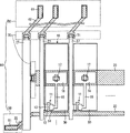
图20是示出图19所示的比较用的有源矩阵基板中的促进腐蚀成分的进入路径的端子电极附近的截面图。 FIG. 20 is a cross-sectional view showing the entry path of a corrosion-promoting component in the comparative active matrix substrate shown in FIG. 19 near the terminal electrodes. the
图21是示出专利文献1记载的有源矩阵基板中的连接部的构成的截面图。
FIG. 21 is a cross-sectional view showing the configuration of a connection portion in the active matrix substrate described in
图22是示出专利文献2记载的有源矩阵基板中的连接端子部的构成的平面图。 FIG. 22 is a plan view showing a configuration of a connection terminal portion in the active matrix substrate described in Patent Document 2. FIG. the
具体实施方式 Detailed ways
〔实施方式1〕 [Implementation 1]
主要根据图1(a)、(b)以及图7(a)~(c)、图19和图20如 下说明本发明的一个实施方式。 An embodiment of the present invention will be explained mainly based on Fig. 1(a), (b) and Fig. 7(a) to (c), Fig. 19 and Fig. 20 as follows. the
图2是示出本实施方式的液晶显示装置的主要部分的概要构成的框图。 FIG. 2 is a block diagram showing a schematic configuration of a main part of a liquid crystal display device according to the present embodiment. the
如图2所示,本实施方式的液晶显示装置1具备:矩阵状地配置有像素10的液晶面板2(显示面板);驱动该液晶面板2的驱动电路;以及控制该驱动电路的驱动的控制电路3,根据需要具备背光源单元(未图示)等。
As shown in FIG. 2 , the liquid
在上述液晶面板2中设有多个扫描配线22和与各扫描配线22分别交叉的多个信号配线27,按这些扫描配线22和信号配线27的每个组合设有像素10(像素部)。另外,根据需要,在与扫描配线22相同的层中配置辅助电容配线23,辅助电容配线23横穿各像素10,与上述扫描配线22大致平行地延伸配置。
The liquid crystal panel 2 is provided with a plurality of
另外,上述驱动电路具备驱动液晶面板2中的扫描配线22的扫描配线驱动电路4和驱动信号配线27的信号配线驱动电路5,根据需要具备驱动辅助电容配线23的辅助电容配线驱动电路6。这些扫描配线驱动电路4、信号配线驱动电路5和辅助电容配线驱动电路6分别与扫描配线22、信号配线27和辅助电容配线23电连接,能从外部对这些金属配线独立地提供电位。这些驱动电路与上述控制电路3分别电连接,由从该控制电路3提供的控制信号、视频信号控制。
In addition, the drive circuit includes a scan line drive circuit 4 for driving the
图3是示出图2所示的液晶显示装置中的液晶面板的概要构成的立体图。 3 is a perspective view showing a schematic configuration of a liquid crystal panel in the liquid crystal display device shown in FIG. 2 . the
如图3所示,液晶面板2具有如下构成:在设有未图示的驱动元件(开关元件)的有源矩阵基板20(元件基板,配线基板)与相对基板80之间设有液晶层92(参照图1(b))。另外,在有源矩阵基板20和相对基板80的与相互相对的面相反的面侧,根据需要设有未图示的相位差板和偏光板。
As shown in FIG. 3 , the liquid crystal panel 2 has a structure in which a liquid crystal layer is provided between an active matrix substrate 20 (element substrate, wiring substrate) provided with unillustrated driving elements (switching elements) and a
如图3所示,与相对基板80比较,有源矩阵基板20形成为面积较大。有源矩阵基板20和相对基板80由沿着相对基板80的端缘设置的密封剂91相互贴合。
As shown in FIG. 3 , the
构成上述液晶层92的液晶材料封入密封剂91的内侧的区域(也 就是说,用由密封剂91包围的有源矩阵基板20和相对基板80形成的单元的内部)。
The liquid crystal material constituting the liquid crystal layer 92 is enclosed in a region inside the sealant 91 (that is, the inside of the cell formed by the
有源矩阵基板20具备:显示区域41,其显示被观察者视觉识别的图像;以及非显示区域42,其设于显示区域的外侧,不被观察者视觉识别图像。
The
有源矩阵基板20和相对基板80隔着液晶层92而相对,密封剂91的内侧的区域是显示区域41。另一方面,非显示区域42由设有密封剂91的密封部43和密封部43的外侧的连接部44(周边端子区域)构成。
The
在上述有源矩阵基板20的周边部从上述相对基板80伸出的区域,作为连接部44形成有从上述单元的内部(显示区域41)引出的扫描配线22和信号配线27等金属配线的引出配线和它们的端子部(参照图4)。
In the region where the peripheral portion of the
连接部44的各端子电极利用ACF等与外部设备电连接,具体地说,与上述扫描配线驱动电路4、信号配线驱动电路5等驱动用IC(集成电路)、驱动用LSI(大规模集成电路)或者搭载有这些驱动电路的TCP、COF(Chip On Film:覆晶薄膜)等挠性配线基板(柔性印刷配线基板:FPC基板)的配线的输出端子电连接。
Each terminal electrode of the connecting
图4是示出图3所示的液晶面板中的有源矩阵基板20中的主要部分的配线结构的平面图。在本实施方式中,作为上述有源矩阵基板20,举出使用了具备TFT作为驱动元件的TFT基板的情况的例子进行说明。
FIG. 4 is a plan view showing the wiring structure of main parts in the
如图4所示,在有源矩阵基板20中,在由上述密封剂91包围的单元的内部,多个扫描配线22和多个信号配线27交叉地配置。在这些扫描配线22和信号配线27的交叉部附近,分别形成有具有TFT11作为驱动元件(开关元件)的像素10(像素部)。在各像素10中分别设有像素电极30。
As shown in FIG. 4 , in the
TFT11的扫描电极12与扫描配线22连接。另外,信号电极13与信号配线27连接。漏极电极14通过漏极配线15与上述像素电极30电连接。由此,在各像素10中,当选择扫描配线22时,TFT11导通, 根据从控制电路3输入的显示数据信号而决定的信号电压由信号配线驱动电路5通过信号配线27施加到液晶面板2。液晶面板2在扫描配线22的选择期间结束而TFT11截止的期间,理想的是持续保持截止时的电压。
另外,如上所述,在与扫描配线22相同的层中配置有辅助电容配线23,辅助电容配线23横穿各像素10,与上述扫描配线22大致平行地延伸配置。
In addition, as described above, the
在上述辅助电容配线23上,从漏极配线15延伸的中间电极16按每个像素10隔着未图示的栅极绝缘膜24(参照图6(e))设于与漏极电极14相同的层。
On the
上述中间电极16通过接触孔17与像素电极30电连接。上述辅助电容配线23和中间电极16发挥按每个像素10形成的辅助电容用的电极的功能。根据本实施方式,能利用形成于上述辅助电容配线23和中间电极16之间的辅助电容来使像素电位稳定。在此,上述辅助电容配线23和中间电极16根据需要而形成即可,并不是必须的。
The above-mentioned
如图4所示,在上述有源矩阵基板20的连接部44设有扫描配线连接部50、信号配线连接部60、配线连接部70,并且根据需要设有未图示的辅助电容配线连接部等。
As shown in FIG. 4 , the
在扫描配线连接部50,设有扫描配线22用于接受外部的信号的扫描端子51(端子电极)和扫描配线22的引出配线。在信号配线连接部60,设有信号配线27用于接受外部的信号的信号端子61(端子电极)和信号配线27的引出配线(与信号配线27连接的连接配线62)。配线连接部70用于将设有上述扫描配线22的第1金属配线层(栅极金属层)和设有信号配线27的第2金属配线层(源极金属层)进行电连接。另外,在未图示的辅助电容配线连接部,设有辅助电容配线23用于接受外部的信号的信号端子(端子电极)。
Scanning terminals 51 (terminal electrodes) for receiving external signals of the
下面参照图6(e)如下说明构成上述有源矩阵基板20的各层。
Each layer constituting the above-mentioned
此外,在以下的说明中,作为连接部44中的层叠结构,举出扫描配线连接部50中的层叠结构为例进行说明。
In addition, in the following description, the laminated structure in the scanning
然而,只看层叠结构,信号配线连接部60中的层叠结构与扫描 配线连接部50中的层叠结构具有相同的结构。也就是说,如图4所示,信号配线27由设于配线连接部70的接触孔71电连接到与扫描配线22设于同一层的连接配线62。
However, looking only at the laminated structure, the laminated structure in the signal wiring connection portion 60 has the same structure as that in the scanning
因此,如上所述,信号配线27的端子部由配线连接部70进行从源极金属层到栅极金属层的转接(换层),由此与扫描配线22形成于同一层。在信号配线连接部60,设有与扫描配线22形成于同一层的连接配线62代替扫描配线22的引出配线。
Therefore, as described above, the terminal portion of the
此外,如上所述,上述配线连接部70可以设于密封剂91的外侧(单元外),也可以设于密封剂91的内部(单元内)。
In addition, as described above, the
图6(a)~(e)是按工序顺序示出上述有源矩阵基板20的制造工序的上述有源矩阵基板20的截面图。此外,图6(a)~(e)分别左右并排示出扫描配线连接部50的截面以及像素10的TFT11附近的截面作为各工序结束时刻的上述有源矩阵基板20的非显示区域42和显示区域41的截面。
6( a ) to ( e ) are cross-sectional views of the
如图6(e)所示,本实施方式的有源矩阵基板20具备玻璃基板21作为透明的绝缘性基板(基底基材,配线保持手段)。
As shown in FIG. 6( e ), the
此外,上述绝缘性基板不一定必须是玻璃基板,也可以是例如塑料基板等。另外,上述绝缘性基板不一定必须是透明的,只要上述有源矩阵基板20和相对基板80中的至少一方绝缘性基板具有透光性即可。上述绝缘性基板(基底基材)只要能保持液晶层等显示媒质层以及配线即可,没有特别限定。
In addition, the above-mentioned insulating substrate does not necessarily have to be a glass substrate, and may be, for example, a plastic substrate or the like. In addition, the above-mentioned insulating substrate does not necessarily have to be transparent, as long as at least one of the above-mentioned
首先,说明上述有源矩阵基板20中的显示区域41的层叠结构。
First, the stacked structure of the
上述有源矩阵基板20具有如下结构:在显示区域41中,在玻璃基板21上,按每个像素10设有TFT11作为驱动元件。具体地说,在玻璃基板21上按顺序设有第1金属配线层(栅极金属层)、栅极绝缘膜24、沟道层25(半导体层)、电极接触层26(半导体层)、第2金属配线层(源极金属层)、保护膜28(钝化膜)、层间绝缘膜29、像素电极30。另外,在上述像素电极30上根据需要设有未图示的取向膜。
The above-mentioned
上述第1金属配线层包括:扫描电极12(例如上层扫描电极12b /下层扫描电极12a)和扫描配线22(例如上层扫描配线22b/下层扫描配线22a)、辅助电容配线23(参照图4:例如上层辅助电容配线/下层辅助电容配线)、连接配线62(参照图4:例如上层连接配线/下层连接配线)等。另外,第2金属配线层包括:信号电极13(例如上层信号电极13b/下层信号电极13a)、漏极电极14(例如上层漏极电极14b/下层漏极电极14a)、信号配线27(参照图4:例如上层信号配线/下层信号配线)、漏极配线15(参照图4:例如上层漏极配线/下层漏极配线)、中间电极16(参照图4:例如上层中间电极/下层中间电极)等。
The above-mentioned first metal wiring layer includes: scanning electrodes 12 (such as
如图6(e)所示,TFT11具有按顺序层叠有扫描电极12、栅极绝缘膜24、沟道层25、电极接触层26、信号电极13和漏极电极14的结构。另外,为了防止金属膜的剥离,如上所述,上述TFT11以及第2金属配线层的表面由保护膜28保护。
As shown in FIG. 6( e ),
下面说明上述有源矩阵基板20中的扫描配线连接部50的层叠结构。
Next, the stacked structure of the scanning
如图6(e)所示,在扫描配线连接部50,从单元的内部(显示区域21)作为引出配线延伸配置有与上述扫描电极12(显示用电极)连接的扫描配线22。
As shown in FIG. 6( e ),
在扫描配线连接部50中的扫描配线22上,按顺序层叠有栅极绝缘膜24、第1半导体层31、保护膜28、层间绝缘膜29、透明电极33。另外,在上述扫描配线22的端部形成有透明电极33直接层叠在上述扫描配线22上的端子部55。
A
如上所述,设于像素部的扫描配线22、栅极绝缘膜24、层间绝缘膜29延伸配置到扫描配线连接部50。此外,在信号配线连接部60,设于像素部的信号配线27、栅极绝缘膜24、层间绝缘膜29延伸配置到信号配线连接部60。这些第1金属配线层、栅极绝缘膜24、层间绝缘膜29由显示区域41和非显示区域42(连接部44)共同使用。
As described above, the
另外,如图6(e)所示,第1半导体层31与沟道层25形成于同一层。即,上述第1半导体层31能用与沟道层25相同的材料同时形成。
In addition, as shown in FIG. 6( e ), the
另外,如图6(e)所示,在层间绝缘膜29上形成的像素电极30和透明电极33形成于同一层。即,透明电极33用与像素电极30相同的材料同时形成。
In addition, as shown in FIG. 6( e ), the
优选上述第1金属配线层和第2金属配线层是低电阻金属膜。特别是,近年来随着显示装置的高精细化、大画面化,强烈希望金属配线的低电阻化。 Preferably, the first metal wiring layer and the second metal wiring layer are low-resistance metal films. In particular, in recent years, along with the increase in the definition and size of display devices, the reduction in the resistance of metal wiring is strongly desired. the
因此,作为构成上述第1金属配线层和第2金属配线层的金属材料,适用Al(铝)、Cu(铜)等低电阻金属或者其合金(例如Cu合金;以下将低电阻金属及其合金统一简称为“低电阻金属”)。 Therefore, as the metal material constituting the first metal wiring layer and the second metal wiring layer, low-resistance metals such as Al (aluminum) and Cu (copper), or alloys thereof (for example, Cu alloys; hereinafter, low-resistance metals and Its alloys are collectively referred to as "low-resistance metals"). the
上述第1金属配线层和第2金属配线层分别可以具有单层结构,也可以具有双层结构或者3层结构等层叠结构。这样,使上述第1金属配线层和第2金属配线层为层叠结构,从而与仅为1层的情况相比具有难以断线的优点。 Each of the first metal wiring layer and the second metal wiring layer may have a single-layer structure, or may have a stacked structure such as a double-layer structure or a three-layer structure. In this way, the above-mentioned first metal wiring layer and second metal wiring layer have a laminated structure, which has an advantage that it is less likely to be disconnected than in the case of only one layer. the
如上所述,在使上述第1金属配线层和第2金属配线层为层叠结构的情况下,优选这些第1金属配线层和第2金属配线层中的上层金属配线层采用上述低电阻金属。 As described above, when the first metal wiring layer and the second metal wiring layer have a stacked structure, it is preferable that the upper metal wiring layer of the first metal wiring layer and the second metal wiring layer use the aforementioned low-resistance metals. the
另一方面,下层金属配线层没有特别限定,能使用例如Cr(铬)、Ti(钛)、Ta(钽)、Mo(钼)或者它们的合金(例如Mo-Ti合金)等。 On the other hand, the lower metal wiring layer is not particularly limited, and for example, Cr (chromium), Ti (titanium), Ta (tantalum), Mo (molybdenum), or alloys thereof (for example, Mo-Ti alloys) can be used. the
如后所述,例如在包括Cu的上层金属配线层之下设有包括Ti的下层金属配线层,由此能使上述第1金属配线层与玻璃基板21良好地紧贴。
As will be described later, for example, by providing a lower metal wiring layer made of Ti under an upper metal wiring layer made of Cu, the first metal wiring layer and the
另外,上述栅极绝缘膜24和保护膜28采用SiNx(氮化硅)、SiO2(二氧化硅)等无机绝缘膜。此外,这些绝缘膜可以具有单层结构,也可以具有层叠结构。
In addition, inorganic insulating films such as SiNx (silicon nitride) and SiO 2 (silicon dioxide) are used for the above-mentioned
另外,上述沟道层25和第1半导体层31的材料(半导体材料)如后所述能使用例如非晶硅。然而,上述沟道层25和第1半导体层31不限于此,例如也可以使用含有In(铟)、Ga(镓)和Zn(锌)的氧化物即IGZO(In、Ga、Zn、O);ZnO(氧化锌)等氧化物半导体。
In addition, as the material (semiconductor material) of the
另外,如后所述,电极接触层26和后述的第2半导体层32(参照图6(b))使用例如在非晶硅中高浓度地掺杂有n型杂质的n+非晶硅层。然而,上述电极接触层26和第2半导体层32也不限于此,能使用例如在上述例示的半导体材料中掺杂杂质而成的半导体层。
In addition, as will be described later, the
另外,上述层间绝缘膜29采用丙烯酸类树脂等有机绝缘膜。
In addition, an organic insulating film such as acrylic resin is used for the above-mentioned
另外,上述像素电极30和透明电极33采用例如ITO(Indium Tin Oxide:铟锡氧化物)、IZO(Indium Zinc Oxide:铟锌氧化物)等透明导电膜。
In addition, transparent conductive films such as ITO (Indium Tin Oxide: Indium Tin Oxide) and IZO (Indium Zinc Oxide: Indium Zinc Oxide) are used for the above-mentioned
此外,上述各层的形成方法(层叠方法)没有特别限定,能应用以往公知的各种方法。 In addition, the formation method (lamination method) of each of the above-mentioned layers is not particularly limited, and various conventionally known methods can be applied. the
上述有源矩阵基板20在上述扫描配线22的端子部55和信号配线27的未图示的端子部以外的区域与相对基板80贴合。此外,在上述扫描端子51和信号端子61与相对基板80之间,设有用于上述引出配线与相对基板80和外部设备连接的余地。
The
这些扫描端子51和信号端子61被用作与外部设备(具体地说,驱动用IC、驱动用LSI、FPC基板等周边电路)的连接端子。例如,将这些扫描端子51和信号端子61与作为连接到FPC基板的驱动用LSI的封装的TAB(Tape Automated Bonding:卷带自动结合)卷带的端子连接,由此能制造利用上述驱动用LSI来驱动的液晶显示装置。
These
下面,作为连接部44中用于与外部设备连接的连接部,举出扫描配线连接部50的例子,参照图1(a)、(b),更详细地说明扫描配线连接部50、信号配线连接部60和未图示的辅助电容配线连接部的构成。
Next, as a connecting portion used to connect with an external device in the connecting
此外,在以下说明中,作为连接部44中用于与外部设备连接的连接部,举出扫描配线连接部50的例子进行说明。
In addition, in the following description, the scanning
然而,如上所述,信号配线27的端子部用配线连接部70进行从源极金属层到栅极金属层的转接(换层),由此与扫描配线22形成于同一层。同样,在辅助电容配线连接部中,引出配线也由栅极金属层形成。因此,这些扫描配线连接部50、信号配线连接部60和辅 助电容配线连接部70的结构仅有配线的名称不同,结构本身是相同的。
However, as described above, the terminal portion of the
因此,例如,扫描配线连接部50、扫描配线22、扫描端子51、扫描电极12能分别改名为信号配线连接部60、连接配线62、信号端子61、信号电极13。另外,在辅助电容配线连接部中也仅代替各金属层(配线)的名称,能进行同样的改名。
Therefore, for example, the scanning
图1(a)是示出上述有源矩阵基板20中的扫描配线连接部50附近的概要构成的平面图,图1(b)是图1(a)所示的有源矩阵基板20的A-A线向视截面图。
Fig. 1 (a) is a plan view showing a schematic configuration of the vicinity of the scanning
如上所述,在扫描配线连接部50,从由密封剂91包围的单元的内部延伸配置有扫描配线22作为引出配线。
As described above, in the scanning
如图1(b)所示,上述扫描配线22具有在下层扫描配线22a上设有上层扫描配线22b的构成。在此,上述扫描配线22如上所述不限于此。
As shown in FIG. 1( b ), the
如图1(a)、(b)所示,上述扫描配线22除了透明电极33(导电膜)直接层叠在上述扫描配线22上的端子部55,由栅极绝缘膜24和设置在该栅极绝缘膜24上的层间绝缘膜29完全覆盖。上述层间绝缘膜29和栅极绝缘膜24不设于上述端子部55。
As shown in FIG. 1(a) and (b), the above-mentioned
在上述端子部55与密封剂91之间的区域,作为包括与TFT11中的半导体层(沟道层25)相同的半导体层的半导体层(也就是说,由相同材料同时形成于同一层的半导体层)而形成有第1半导体层31。
In the region between the above-mentioned
如图1(a)所示,第1半导体层31与扫描配线22和透明电极33交叉地形成为比扫描配线22和透明电极33的线宽度大的宽度。此外,透明电极33形成为比扫描配线22的线宽度大的宽度。
As shown in FIG. 1( a ), the
这样,第1半导体层31形成为比扫描配线22和透明电极33的线宽度大的宽度,但是为了不与配置于相邻的扫描配线22的第1半导体层31相连,为比相邻的扫描配线22间的间隔(配线间距)窄的宽度。
In this way, the
上述第1半导体层31是发挥用于进行栅极绝缘膜24的图案化 (具体地说,干式蚀刻)的掩模的功能的掩模层。
The
因此,如图1(a)、(b)所示,上述第1半导体层31的端面31a与接触到上述第1半导体层31的栅极绝缘膜24的端面24a相连地形成于栅极绝缘膜24上的面向上述端子部55的栅极绝缘膜24的端部。
Therefore, as shown in FIG. 1(a) and (b), the
此外,在本实施方式中,只要没有特别提到,“端面”都是指与透明电极33直接层叠于扫描配线22上的区域(端子部55)相对的端面。
In addition, in this embodiment, unless otherwise mentioned, "end surface" refers to the end surface facing the area (terminal part 55) in which the
另外,层间绝缘膜29的端面29a与上述第1半导体层31重叠地形成。
In addition, the
因此,上述第1半导体层31设于上述栅极绝缘膜24上的上述层间绝缘膜29的端面29a的延长线上,与该延长线交叉。因此,上述第1半导体层31覆盖上述延长线与扫描配线22交叉的位置的上方。
Therefore, the
上述层间绝缘膜29发挥用于进行扫描配线22上的栅极绝缘膜24和保护膜28的图案化(具体地说,干式蚀刻)的掩模的功能。因此,上述保护膜28的端面28a与层间绝缘膜29的端面29a相连地形成。
The
另外,在存在第1半导体层31的区域中,上述栅极绝缘膜24的端面24a与第1半导体层31的端面31a相连。另一方面,在未设有第1半导体层31的区域中,如图1(a)所示,上述栅极绝缘膜24的端面24a与上述层间绝缘膜29的端面29a相连。
In addition, in the region where the
因此,如图1(a)、(b)所示,在存在上述第1半导体层31的区域中,上述第1半导体层31和栅极绝缘膜24的一部分从层间绝缘膜29的端面29a向端子部55侧延伸。也就是说,上述第1半导体层31和栅极绝缘膜24的一部分比层间绝缘膜29的端面29a向端子部55侧突出。
Therefore, as shown in FIGS. Extends toward the
因此,与上述端子部55相对的栅极绝缘膜24的端面24a位于比与上述端子部55相对的层间绝缘膜29的端面29a靠上述端子部55侧的位置。换言之,与上述端子部55相对的层间绝缘膜29的端面29a设为比与上述端子部55相对的栅极绝缘膜24的端面24a远离上述端子部55。
Therefore, the
这样,从上述层间绝缘膜29的端面29a向端子部55侧延伸的上述第1半导体层31和栅极绝缘膜24发挥将作为金属配线层的上述扫描配线22(特别是,上述端子部55)从层间绝缘膜29的端面29a以及该端面29a中的透明电极33隔离的隔离壁(隔离层)的功能。
In this way, the
透明电极33覆盖上述层间绝缘膜29上和层间绝缘膜29的端面29a、保护膜28的端面28a、第1半导体层31上及其端面31a、栅极绝缘膜24的端面24a,延伸配置到上述端子部55。覆盖在上述端子部55的扫描配线22上的上述透明电极33被用作通过ACF93(粘接层)与外部设备连接的扫描端子51(端子电极)。
The
如图1(a)所示,上述透明电极33沿着从单元内部引出的扫描配线22延伸配置到端子部,覆盖作为引出配线的扫描配线22整体。
As shown in FIG. 1( a ), the
在上述扫描配线连接部50上,以包括覆盖上述扫描配线22的端子部55的透明电极33的扫描端子51为连接端子,安装有周边电路等外部设备。
External devices such as peripheral circuits are mounted on the scanning
如图1(a)所示,扫描端子51通过ACF93压接连接于上述周边电路等,将从该周边电路等施加的电压通过上述扫描配线22提供扫描电极12。
As shown in FIG. 1( a ), the
下面,参照图5、图19和图20说明上述有源矩阵基板20中的促进腐蚀成分的侵入防止效果。
Next, the intrusion prevention effect of the corrosion-promoting component in the above-mentioned
此外,在以下的说明中,举出扫描配线连接部50的例子进行说明,但是扫描配线连接部50、扫描配线22、扫描端子51、扫描电极12也能分别改名为信号配线连接部60、连接配线62、信号端子61、信号电极13。
In addition, in the following description, the scanning
图5是用于说明图1(a)、(b)示出的有源矩阵基板20中的促进腐蚀成分的侵入防止效果的扫描端子51附近的截面图。
FIG. 5 is a cross-sectional view of the vicinity of the
另外,图19是示出比较用的有源矩阵基板的扫描配线连接部附近的概要构成的截面图。另外,图20是示出图19所示的比较用的有源矩阵基板中的促进腐蚀成分的进入路径的端子电极附近的截面图。 In addition, FIG. 19 is a cross-sectional view showing a schematic configuration of the vicinity of the scanning wiring connection portion of the active matrix substrate for comparison. In addition, FIG. 20 is a cross-sectional view in the vicinity of the terminal electrode showing the entry path of the corrosion-promoting component in the active matrix substrate for comparison shown in FIG. 19 . the
如图19所示,比较用的有源矩阵基板510具有如下构成:在扫 描配线连接部中,在玻璃基板501上按顺序层叠有扫描配线502、栅极绝缘膜503、保护膜504、层间绝缘膜505、透明电极506。上述扫描配线502从单元内部引出,在其端部形成有透明电极506直接接于上述扫描配线502上而成的端子部550。
As shown in FIG. 19, an
此外,如图21所示,专利文献1在ACF310的贴附位置及其附近部分也形成有层间绝缘膜303。
In addition, as shown in FIG. 21 , in
然而,在图19所示的比较用的有源矩阵基板510中,与图1(a)、(b)示出的有源矩阵基板20同样,在成为端子部550的、ACF的贴附位置(扫描端子540)及其附近部分未设有层间绝缘膜505、保护膜504和栅极绝缘膜503。
However, in the
为了补偿配线引起的凹凸,作为平坦化膜的层间绝缘膜采用容易厚膜化的有机绝缘膜。然而,与无机绝缘膜相比,有机绝缘膜一般对机械应力、热应力较弱,容易产生裂缝。 In order to compensate unevenness caused by wiring, an organic insulating film that is easy to thicken is used as an interlayer insulating film as a planarizing film. However, compared with inorganic insulating films, organic insulating films are generally weaker against mechanical stress and thermal stress, and are prone to cracks. the
在有源矩阵基板的端子部(端子电极),通过ACF连接着驱动电路(周边电路)等外部设备。因此,在该端子部中的外部设备的安装工序、基板分断工序(切割)等时,有源矩阵基板中的从相对基板伸出的区域容易被施加应力。 External devices such as drive circuits (peripheral circuits) are connected to terminal portions (terminal electrodes) of the active matrix substrate via ACF. Therefore, stress is likely to be applied to the region of the active matrix substrate protruding from the counter substrate during the process of mounting external devices in the terminal portion, the process of separating the substrate (dicing), and the like. the
因此,希望在有源矩阵基板的端子部(具体地说,ACF的贴附位置及其周边部分)不设置层间绝缘膜(平坦化膜)。 Therefore, it is desirable not to provide an interlayer insulating film (planarizing film) on the terminal portion of the active matrix substrate (specifically, the attachment position of the ACF and its peripheral portion). the
此外,在通过导电性粒子实现外部设备与端子电极的电连接的ACF的特性上,当在ACF贴附位置的端子电极与其以外的部分之间存在大的台阶时,导电性粒子与端子电极接触的概率变低,产生电连接不良的概率变大。因此,希望在有源矩阵基板的端子部(具体地说,ACF的贴附位置及其周边部分)不设置膜厚大的有机层间绝缘膜(平坦化膜)。 In addition, in terms of the characteristics of ACF in which electrical connection between external devices and terminal electrodes is realized by conductive particles, when there is a large step between the terminal electrode at the ACF attachment position and other parts, the conductive particles will come into contact with the terminal electrodes. The probability becomes lower, and the probability of poor electrical connection becomes higher. Therefore, it is desirable not to provide a thick organic interlayer insulating film (planarizing film) on the terminal portion of the active matrix substrate (specifically, the attachment position of the ACF and its peripheral portion). the
因此,在有源矩阵基板的端子部,将层间绝缘膜以不覆盖端子部的方式形成图案。因此,在有源矩阵基板的连接部,为了露出端子部的金属配线,将该层间绝缘膜作为掩模对下层的保护膜和栅极绝缘膜进行蚀刻除去(干式蚀刻)。 Therefore, the interlayer insulating film is patterned on the terminal portion of the active matrix substrate so as not to cover the terminal portion. Therefore, in the connection portion of the active matrix substrate, in order to expose the metal wiring of the terminal portion, the protective film and the gate insulating film of the lower layer are etched and removed by using the interlayer insulating film as a mask (dry etching). the
在具有这种构成的有源矩阵基板中,用于端子电极的ITO等透 明导电膜与扫描配线表面的紧贴性良好,另外,上述透明导电膜比较致密地形成。 In the active matrix substrate having such a configuration, the transparent conductive film such as ITO used for the terminal electrodes has good adhesion to the surface of the scanning wiring, and the transparent conductive film is relatively densely formed. the
因此,在具有这种构成的上述有源矩阵基板20、510中,几乎不会以端子部55、550为起点发生腐蚀,另外,在这些端子部55、550难以进行腐蚀。
Therefore, in the
然而,在任何情况下,在溅射覆盖层间绝缘膜29、505的透明电极33、506之前的阶段,如上所述,都需要除去端子部55、550的层间绝缘膜29、505、保护膜28、504和栅极绝缘膜24、503。此时,经过将图案化的层间绝缘膜29、505作为掩模对栅极绝缘膜24、503和保护膜28、504进行干式蚀刻的工序之后,溅射透明电极33、506之前,对层间绝缘膜29、505的表面造成了损伤。
However, in any case, at the stage before the sputtering of the
其结果是,层间绝缘膜29、505的表面粗糙度成为大的状态(例如凹凸的水平为20nm~50nm),与层间绝缘膜29、505接触的部分的透明电极33、506无法致密地形成,如图5和图20所示,有可能在该部分的透明电极33、506产生缺陷33a、506a。
As a result, the surface roughness of the interlayer insulating
在图19和图20所示的有源矩阵基板510中,将图案化的层间绝缘膜505作为掩模对栅极绝缘膜503和保护膜504进行干式蚀刻,由此,层间绝缘膜505的端面505a、与扫描配线502接触的栅极绝缘膜503的端面503a以及其间的保护膜504的端面504a分别相连。
In the
因此,当上述透明电极506(特别是与上述层间绝缘膜505的端面505a接触的部分)中存在缺陷506a时,如图20所示,有时水分等促进腐蚀成分从该缺陷506a通过上述层间绝缘膜505的端面505a、保护膜504的端面504a和栅极绝缘膜503的端面503a侵入,促进腐蚀成分会侵入与上述端面503a接触的扫描配线22。
Therefore, when there is a
因此,在图19和图20所示的有源矩阵基板510中,在上述扫描配线502采用Cu等低电阻配线材料的情况下,接近上述缺陷506a的扫描配线502有时会发生腐蚀。
Therefore, in the
其结果是,在图18和图19所示的有源矩阵基板510中,扫描配线502与透明电极506直接紧贴的部分和被栅极绝缘膜503以及保护膜504覆盖的部分发生腐蚀的概率低,而当接近缺陷506a的扫描配 线502暂时发生腐蚀时,能见到沿着扫描配线502暂时发生腐蚀时,能见到沿着扫描配线502与透明电极506的界面和扫描配线502与栅极绝缘膜503的界面进行腐蚀的现象。
As a result, in the
与此相对,根据本实施方式,如上所述,在栅极绝缘膜24与层间绝缘膜29之间(具体地说,与栅极绝缘膜24相邻),第1半导体层31形成为层间绝缘膜29的端面29a与第1半导体层31重叠。因此,上述第1半导体层31发挥用于进行栅极绝缘膜24的干式蚀刻的掩模的功能。
On the other hand, according to the present embodiment, as described above, the
其结果是,如上所述,在存在第1半导体层31的区域中,第1半导体层31的一部分以及栅极绝缘膜24的一部分从层间绝缘膜29的端面29a向端子部55侧延伸,由此,上述层间绝缘膜29的端面29a比栅极绝缘膜24的端面24a远离端子部55设置。
As a result, as described above, in the region where the
此外,如上所述在层间绝缘膜29与透明电极33的接触面以外的部分,各层紧贴地形成,另外,与有机膜相比,无机膜具有致密的结构。另外,通过如上所述地层叠第1半导体层31,与缺陷33a的物理距离也被扩大。因此,不会发生促进腐蚀成分从上述端面24a以外的部分侵入。
In addition, as described above, the layers are formed in close contact at portions other than the contact surface between the interlayer insulating
因此,如图5所示,即使在透明电极33中,在该透明电极33覆盖层间绝缘膜29的部分产生了缺陷33a,该缺陷33a到其下层的栅极绝缘膜24与扫描配线22接触的部分(特别是与扫描配线22接触的栅极绝缘膜24的端面24a)之间的距离也保持为较大。另外,利用第1半导体层31将干式蚀刻后的栅极绝缘膜24的表面皲裂抑制为比较小。因此,覆盖栅极绝缘膜24的端面24a的部分的透明电极33变致密,防止促进腐蚀成分的侵入、迂回进入。
Therefore, as shown in FIG. 5, even in the
因此,根据本实施方式,即使层间绝缘膜29的表面粗糙,在层间绝缘膜29上的透明电极33中产生了缺陷33a,也能防止层间绝缘膜29的表面的状态引起的扫描配线22和扫描电极12的腐蚀和断线。
Therefore, according to the present embodiment, even if the surface of the
另外,根据本实施方式,如上所述,上述透明电极33不仅覆盖端子部55至第1半导体层31的上表面,还覆盖层间绝缘膜29。因此,即使由于透明电极33的图案对准不良而在透明电极33中的密封剂91侧的端缘产生位置偏移,该透明电极33中的密封剂91侧的端缘也 不会比第1半导体层31向端子部55侧(边界)移动(位置偏移)。因此,扫描配线22的表面(特别是,接近层间绝缘膜29的端面29a的扫描配线22的表面)不会露出。
In addition, according to the present embodiment, as described above, the
另外,如上所述设置第1半导体层31,使层间绝缘膜29的端面29a与栅极绝缘膜24的端面24a分离,由此能使利用该栅极绝缘膜24和第1半导体层31如上所述从层间绝缘膜29的表面至端子部55设置的透明电极33跨过的台阶分级。其结果是,能提高透明电极33的覆盖性。
In addition, the
下面参照图6(a)~(e)如下说明上述有源矩阵基板20的制造方法。本实施方式中的有源矩阵基板20利用5次光刻工序制造。
Next, a method of manufacturing the above-mentioned
〔扫描配线形成工序〕 〔Scan wiring formation process〕
图6(a)示出如下状态:在玻璃基板21上作为金属配线形成有包括下层扫描配线22a和上层扫描配线22b的双层结构的扫描配线22,并且设有包括设于该扫描配线22的下层扫描电极12a和上层扫描电极12b的双层结构的扫描电极12。此外,在本制造例中,举例说明下层扫描电极12a和下层扫描配线22a采用Ti,上层扫描电极12b和上层扫描配线22b采用Cu的情况。也就是说,在本制造例中,举例说明包括扫描配线22的第1金属配线(栅极金属层)具有作为上层金属配线/下层金属配线的Ti/Cu的层叠结构(双层结构)的情况。
6(a) shows a state in which a
首先,利用溅射法在玻璃基板21上按顺序连续形成包括Ti、Cu的两种导电膜。
First, two types of conductive films including Ti and Cu are successively formed sequentially on the
然后,在上述导电膜上利用光刻形成抗蚀剂图案。然后进行湿式蚀刻,将上述导电膜图案化后,对上述抗蚀剂图案进行剥离清洗。由此,在像素10中形成扫描电极12,所述扫描电极12具有在下层扫描电极12a上设有上层扫描电极12b的Cu/Ti的双层结构。另外,与此同时,在玻璃基板21上形成在下层扫描配线22a上设有上层扫描配线22b的具有Cu/Ti的双层结构的扫描配线22,将其作为显示区域41中的显示用电极以及扫描配线连接部50中的引出配线和端子电极。
Then, a resist pattern was formed on the above-mentioned conductive film by photolithography. Thereafter, wet etching was performed to pattern the conductive film, and then the resist pattern was peeled and cleaned. Thus, scanning
此外,此时将上述导电膜图案化,由此如图2和图4所示,能形成连接配线62,根据需要能形成辅助电容配线23。此外,在后述的实施方式中说明信号配线27与连接配线62的转接,在本实施方式中省略。
In addition, at this time, by patterning the above-mentioned conductive film, as shown in FIGS. 2 and 4 ,
在本工序中,虽未特别限定,但是优选Ti膜以20~150nm的厚度,Cu膜以200~500nm的厚度成膜。 In this step, although not particularly limited, the Ti film is preferably formed to have a thickness of 20 to 150 nm, and the Cu film to be formed to have a thickness of 200 to 500 nm. the
〔栅极绝缘膜/半导体层形成工序〕 〔Gate insulating film/semiconductor layer formation process〕
在本工序中,首先,如图6(b)所示,利用CVD法形成包括氮化硅(SiNx)的栅极绝缘膜24(无机绝缘膜),使其覆盖上述扫描电极12和扫描配线22。然后,在上述栅极绝缘膜24上形成非晶硅层、以高浓度掺杂了n型杂质的n+非晶硅层作为半导体层之后,利用光刻形成抗蚀剂图案。然后,进行干式蚀刻,将上述半导体层图案化之后,对上述抗蚀剂图案进行剥离清洗。
In this step, first, as shown in FIG. 6(b), a gate insulating film 24 (inorganic insulating film) made of silicon nitride (SiNx) is formed by CVD so as to cover the above-mentioned
由此,如图6(b)所示,在各像素10中的栅极绝缘膜24上形成包括上述非晶硅层的沟道层25和包括层叠在该沟道层25上的n+非晶硅层的电极接触层26。另外,在扫描配线连接部50中的栅极绝缘膜24上形成包括上述非晶硅层的第1半导体层31,并且在该第1半导体层31上形成包括n+非晶硅层的第2半导体层32。
As a result, as shown in FIG. 6( b ), a
此外,虽未图示,但是通过上述工序,在信号配线连接部60中的栅极绝缘膜24上也形成与上述第1半导体层31和第2半导体层32同样的半导体层。也就是说,在信号配线连接部60也用与扫描配线连接部50中的第1半导体层31和第2半导体层32相同的材料在同一层并且同时形成与扫描配线连接部50中的第1半导体层31和第2半导体层32分离的第1半导体层31和第2半导体层32。
In addition, although not shown, the same semiconductor layers as the above-mentioned
在本工序中没有特别限定,优选以200~500nm的厚度形成构成上述栅极绝缘膜24的氮化硅膜。另外,优选以30~300nm的厚度形成构成上述沟道层25和第1半导体层31的非晶硅层,以20~150nm的厚度形成构成电极接触层26和第2半导体层的n+非晶硅层。
Although not particularly limited in this step, it is preferable to form the silicon nitride film constituting the
〔信号配线形成工序〕 〔Signal wiring forming process〕
然后,虽未图示,在上述栅极绝缘膜24上作为金属配线形成包括下层信号配线和上层信号配线的双层结构的信号配线27(参照图2和图4)和漏极配线15(参照图4)。另外,此时,如图6(c)所示,以覆盖上述电极接触层26的方式,在上述栅极绝缘膜24上形成包括设于上述信号配线27的下层信号电极13a和上层信号电极13b的双层结构的信号电极13以及包括下层漏极电极14a和上层漏极电极14b的双层结构的漏极电极14。
Next, although not shown, signal wiring 27 (refer to FIGS. 2 and 4 ) of a double-layer structure including a lower layer signal wiring and an upper layer signal wiring and a drain electrode are formed on the
此外,在本制造例中,举例说明了未图示的下层信号配线、下层信号电极13a和下层漏极电极14a采用Ti,未图示的上层信号配线、上层信号电极13b和上层漏极电极14b采用Cu的情况。也就是说,在本制造例中,举例说明了包括信号电极13的第2金属配线(源极金属层)具有作为上层金属配线/下层金属配线的Ti/Cu的层叠结构(双层结构)的情况。
In addition, in this manufacturing example, Ti is used for the unillustrated lower layer signal wiring, the lower layer signal electrode 13a, and the lower
在本工序中,首先,在上述栅极绝缘膜24上通过溅射法按顺序连续形成包括Ti、Cu的两种导电膜,使其覆盖上述电极接触层26。
In this step, first, two types of conductive films including Ti and Cu are successively formed on the
在上述导电膜上,通过光刻形成抗蚀剂图案。然后进行湿式蚀刻,将上述导电膜图案化之后,对上述抗蚀剂图案进行剥离清洗。 On the above conductive film, a resist pattern is formed by photolithography. After performing wet etching and patterning the said conductive film, the said resist pattern was peeled and cleaned. the
由此,在像素10中形成信号电极13,所述信号电极13具有在下层信号电极13a上设有上层信号电极13b的Cu/Ti的双层结构。另外,形成与上述信号配线27分离的具有在下层漏极电极14a上设有上层漏极电极14b的Cu/Ti的双层结构的漏极电极14以及从该漏极电极14延伸的漏极配线15(参照图4)。另外,与此同时,作为显示区域41中的显示用电极以及引出配线的一部分(具体地说,用于配线连接部44中的换层的引出配线),形成具有在下层信号配线上设有上层信号配线的Cu/Ti的双层结构的信号配线27(参照图2和图4)。
Thus, the
然后,通过干式蚀刻对作为沟道部的区域的电极接触层26进行除去(沟道蚀刻),并且在整个面除去第2半导体层32。此外,此时,对上述作为沟道部的区域的沟道层25的表面进行蚀刻,由此调整厚度,形成沟道部。然后,对上述抗蚀剂图案进行剥离清洗。由此, 形成TFT11。
Then, the
在本工序中虽未特别限定,优选以20~150nm的厚度形成Ti膜,以200~500nm的厚度形成Cu膜。 Although not particularly limited in this step, it is preferable to form a Ti film with a thickness of 20 to 150 nm, and to form a Cu film with a thickness of 200 to 500 nm. the
〔保护膜/层间绝缘膜形成工序〕 〔Protective film/interlayer insulating film formation process〕
在本工序中,首先,在上述栅极绝缘膜24上通过CVD法形成氮化硅(SiNx)膜作为保护膜28(钝化膜,无机绝缘膜),使其覆盖上述信号配线27、信号电极13、漏极电极14。
In this step, first, a silicon nitride (SiNx) film is formed as a protective film 28 (passivation film, inorganic insulating film) on the above-mentioned
然后,利用旋涂法在上述氮化硅膜上形成包括感光性树脂材料的层间绝缘膜材料,然后,通过光刻进行图案化之后进行干式蚀刻。由此,将包括上述氮化硅膜的保护膜28和包括上述层间绝缘膜材料的层间绝缘膜29(有机绝缘膜,平坦化膜)形成图案。
Then, an interlayer insulating film material including a photosensitive resin material is formed on the above-mentioned silicon nitride film by a spin coating method, and then, after patterning by photolithography, dry etching is performed. Thus, the
此外,此时,对于上述层间绝缘膜29,考虑到图案化的位置偏移或者后述的干式蚀刻中的蚀刻精度,希望其端面29a与上述第1半导体层31的上表面重叠地进行图案化。
In addition, at this time, the
通过以上述层间绝缘膜29为掩模的干式蚀刻,虽未图示,在像素10中,保护膜28中的未被遮住的部分被除去,露出信号电极13和漏极电极14。
By dry etching using the
另一方面,在扫描配线连接部50,如图6(d)所示,通过以上述层间绝缘膜29为掩模的干式蚀刻,除去作为引出配线的扫描配线22上的栅极绝缘膜24和保护膜28中的未被遮住的部分。由此,露出端子部55(扫描端子51(参照图1(a))及其附近)的扫描配线22。
On the other hand, in the scanning
此时,如图6(d)所示,在扫描配线连接部50,在延长了层间绝缘膜29的端面29a时,第1半导体层31被配置在该端面29a与扫描配线22交叉的位置。因此,该第1半导体层31在干式蚀刻时发挥掩模的作用。
At this time, as shown in FIG. 6( d ), when the
其结果是,如图6(d)和图1(a)、(b)所示,在存在第1半导体层31的区域中,第1半导体层31的一部分以及栅极绝缘膜24的一部分为从层间绝缘膜29的端面29a延伸(也就是说突出)的结构。
As a result, as shown in FIG. 6(d) and FIG. 1(a), (b), in the region where the
另外,虽未图示,与扫描配线连接部50同样,在信号配线连接部60,通过以上述层间绝缘膜29为掩模的干式蚀刻,除去作为信号 配线27的引出配线的连接配线62上的栅极绝缘膜24和保护膜28中未被遮住的部分。由此,端子部(信号端子61及其附近)的连接配线62露出。
In addition, although not shown in the figure, similarly to the scanning
此时,在信号配线连接部60,在延长了层间绝缘膜29的端面时,在该端面与连接配线62交叉的位置配置有与扫描配线连接部50中的第1半导体层31同样的半导体层(第1半导体层31)。因此,该半导体层(第1半导体层31)在干式蚀刻时作为掩模而工作。其结果是,在信号配线连接部60中,第1半导体层31的一部分以及栅极绝缘膜24的一部分为从层间绝缘膜29的端面29a延伸的(即突出的)结构。
At this time, in the signal wiring connection portion 60 , when the end surface of the
此外,在本工序中,没有特别限定,优选以100~700nm的厚度形成氮化硅膜。层间绝缘膜29只要形成为能补偿上述有源矩阵基板20中的各金属配线以及TFT11导致的凹凸的厚度即可,没有特别限定。上述层间绝缘膜例如以0.5μm~10μm的厚度形成。
In addition, in this step, although it is not particularly limited, it is preferable to form a silicon nitride film with a thickness of 100 to 700 nm. The
〔透明导电膜形成工序〕 〔Transparent conductive film formation process〕
在本工序中,通过溅射法在形成有上述层间绝缘膜29的玻璃基板21的上表面整个面上形成包括ITO的透明导电膜。然后,在该透明导电膜上通过光刻形成抗蚀剂图案。然后,进行湿式蚀刻对上述透明导电膜进行图案化后,对上述抗蚀剂图案进行剥离清洗。由此,在各像素10中形成包括上述透明导电膜的像素电极30。
In this step, a transparent conductive film made of ITO is formed by sputtering on the entire upper surface of the
另外,在扫描配线连接部50中,如图6(e)所示,形成包括上述透明导电膜的透明电极33,使得该透明电极33覆盖层间绝缘膜29上和层间绝缘膜29的端面29a、保护膜28的端面28a、第1半导体层31上及其端面31a、栅极绝缘膜24的端面24a以及露出的扫描配线22上。
In addition, in the scanning
如上所述,在露出的扫描配线22上形成上述透明电极33,由此在上述扫描配线22的端部形成扫描端子51(端子电极)。
As described above, the
此外,虽未图示,通过上述工序,在信号配线连接部60中也形成与上述透明电极33同样的透明电极。也就是说,在信号配线连接部60,也用与扫描配线连接部50中的透明电极33相同的材料在同一 层并且同时形成与扫描配线连接部50中的透明电极分离的透明电极33。
In addition, although not shown, a transparent electrode similar to the above-described
此外,与扫描配线连接部50同样,在信号配线连接部60形成包括上述透明导电膜的透明电极33,使得该透明电极33覆盖层间绝缘膜29上和层间绝缘膜29的端面29a、保护膜28的端面28a、第1半导体层31上及其端面31a、栅极绝缘膜24的端面24a以及露出的连接配线62上。
In addition, as in the scanning
如上所述,在露出的连接配线62上形成上述透明电极33,由此在上述连接配线62的端部形成信号端子61(参照图4:端子电极)。
As described above, the
在本工序中,没有特别限定,但是优选以50~200nm的厚度形成上述透明导电膜。 In this step, it is not particularly limited, but it is preferable to form the above-mentioned transparent conductive film with a thickness of 50 to 200 nm. the
〔取向膜形成工序〕 〔Alignment film formation process〕
最后,根据需要,在上述有源矩阵基板20的表面(与相对基板80相对的面)形成未图示的取向膜。上述取向膜能通过印刷法形成例如聚酰亚胺膜来形成。 Finally, if necessary, an alignment film (not shown) is formed on the surface of the active matrix substrate 20 (the surface facing the counter substrate 80 ). The above-mentioned alignment film can be formed by forming, for example, a polyimide film by a printing method. the
通过上述工序,与TFT11的形成同时地在有源矩阵基板20的规定的位置形成扫描配线连接部50、信号配线连接部60和配线连接部70。此外,基于上述有源矩阵基板20的制造工序,通过改变在各工序中形成的图案来制作各连接部。
Through the above-described steps, the scan
下面参照图7(a)~(c)如下说明相对基板80的构成及其制造方法。
Next, the structure of the
图7(a)~(c)是按工序顺序示出上述相对基板80的制造工序的截面图。图7(a)~(c)分别示出各工序结束时刻的上述相对基板80的截面。
7( a ) to ( c ) are cross-sectional views showing the manufacturing steps of the above-mentioned
如图7(c)所示,相对基板80具有在玻璃基板81上按顺序层叠有黑矩阵83和彩色滤光片层82、相对电极84、光间隔物85的构成。
As shown in FIG. 7( c ), the
如以下所示,上述相对基板80是通过3次光刻工序制造的。
As shown below, the above-mentioned
〔黑矩阵/彩色滤光片层的形成工序〕 〔Black matrix/color filter layer formation process〕
在本工序中,如图7(a)所示,通过光刻在玻璃基板81上用感光性材料形成黑矩阵83和彩色滤光片层82。作为上述彩色滤光片 层,形成例如R(红色)、G(绿色)、B(蓝色)的彩色滤光片层。
In this step, as shown in FIG. 7( a ), a
〔相对电极的形成工序〕 〔Formation process of counter electrode〕
下面,如图7(b)所示,通过溅射法在上述玻璃基板81上形成包括ITO的透明导电膜,使其覆盖上述黑矩阵83和彩色滤光片层82。然后,在该透明导电膜上通过光刻形成抗蚀剂图案。然后,进行湿式蚀刻,对上述透明导电膜进行图案化后,对上述抗蚀剂图案进行剥离清洗,由此形成相对电极84。
Next, as shown in FIG. 7( b ), a transparent conductive film including ITO is formed on the
在本工序中,没有特别限定,但是优选以50~200nm的厚度形成上述透明导电膜。 In this step, it is not particularly limited, but it is preferable to form the above-mentioned transparent conductive film with a thickness of 50 to 200 nm. the
〔光间隔物的形成工序〕 〔Photo spacer formation process〕
接下来,如图7(c)所示,用感光性材料通过光刻在上述相对电极84上形成光间隔物85,使其覆盖上述黑矩阵83。
Next, as shown in FIG. 7( c ), a
〔取向膜形成工序〕 〔Alignment film formation process〕
最后,根据需要,在上述相对基板80的表面(与有源矩阵基板20相对的面)形成未图示的取向膜。上述取向膜能通过印刷法形成例如聚酰亚胺膜来形成。通过上述各工序制造相对基板80。
Finally, if necessary, an alignment film (not shown) is formed on the surface of the counter substrate 80 (the surface facing the active matrix substrate 20 ). The above-mentioned alignment film can be formed by forming, for example, a polyimide film by a printing method. The
在此,在本实施方式中,上述各层的厚度、材料以及成膜方法不限于上述具体例,能适当地设定、变更。 Here, in this embodiment, the thicknesses, materials, and film-forming methods of the above-mentioned layers are not limited to the above-mentioned specific examples, and can be appropriately set and changed. the
下面说明本实施方式的液晶面板2的制造方法。 Next, a method for manufacturing the liquid crystal panel 2 of the present embodiment will be described. the
上述液晶面板2能通过在上述有源矩阵基板20的制造工序和相对基板80的制造工序后进行以下的工序来制造。
The liquid crystal panel 2 can be manufactured by performing the following steps after the steps of manufacturing the
〔贴合工序〕 〔Fitting process〕
在本工序中,首先,在有源矩阵基板20和相对基板80中的一方基板上沿着相对基板80的端缘形状印刷密封剂91。然后,对由该密封剂91包围的区域滴下液晶。然后,将上述有源矩阵基板20和相对基板80隔着上述密封剂贴合。
In this step, first, a
〔基板分断工序〕 〔Substrate breaking process〕
接下来,根据需要,将在上述贴合工序中贴合的基板分断(dicing cut:划片切割)。通过以上的工序来形成上述液晶面板2。 Next, if necessary, the substrates bonded in the above-mentioned bonding process are divided (dicing cut: dicing cut). The above-mentioned liquid crystal panel 2 is formed through the above steps. the
然后,针对上述液晶面板2,将设有扫描配线驱动电路4、信号 配线驱动电路5等驱动电路的TCP等外部设备通过ACF93连接到设于有源矩阵基板20所设的连接部44中的对外部设备的连接部(例如,扫描配线连接部50和信号配线连接部60等)的各端子部,由此能制造本实施方式的液晶显示装置1。
Then, for the above-mentioned liquid crystal panel 2, external devices such as TCP provided with driving circuits such as the scanning wiring driving circuit 4 and the signal
由此,能得到能防止金属配线的腐蚀和断线的耐腐蚀性良好的有源矩阵基板20和具备它的液晶面板2以及液晶显示装置1。
Thereby, the
本实施方式的有源矩阵基板20不限于上述液晶面板2和液晶显示装置1,例如能应用于将有机EL或者无机EL作为显示介质的显示面板和显示装置。
The
另外,作为上述显示装置,除了笔记本个人计算机、便携电话机、电子记事本、TV(电视)接收机以外,也能适用于电泳装置中的显示装置等。 In addition, as the above-mentioned display device, it is also applicable to a display device in an electrophoretic device, etc. in addition to a notebook personal computer, a mobile phone, an electronic notebook, and a TV (television) receiver. the
此外,在本实施方式中,如上所述,举例说明了作为掩模层使用与TFT11中的半导体层相同的半导体层的情况。然而,本实施方式不限于此。 In addition, in this embodiment, as mentioned above, the case where the same semiconductor layer as the semiconductor layer in TFT11 was used as a mask layer was exemplified. However, the present embodiment is not limited thereto. the
作为上述掩模层,只要使具有耐蚀刻性(干式耐蚀刻性),发挥用于栅极绝缘膜24的图案化的掩模的功能的层即可,也能与TFT11中的半导体层分别形成。
As the above-mentioned mask layer, as long as it has etching resistance (dry etching resistance) and functions as a mask for patterning the
然而,如上所述使用与TFT11中的半导体层相同的半导体层作为上述掩模层,从而只要变更用于半导体层的图案化的掩模的形状,不用变更工序,就能容易并且低价地形成上述掩模层。
However, by using the same semiconductor layer as the semiconductor layer in
另外,在本实施方式中,在对作为沟道部的区域的电极接触层26进行除去(沟道蚀刻)时,举例说明了除去第2半导体层32的情况,然而本实施方式不限于此。例如,也能使用专用的掩模来保留第2半导体层。
In addition, in this embodiment, the case where the
〔实施方式2〕 [Implementation 2]
基于图8如下说明本发明的其它实施方式。此外,在本实施方式中,主要说明与上述实施方式1的不同点,对具有与上述实施方式1同样的功能的构成要素标注相同的编号,省略说明。 Another embodiment of the present invention will be described below based on FIG. 8 . In addition, in this embodiment, differences from the above-mentioned first embodiment will be mainly described, and components having the same functions as those in the above-mentioned first embodiment will be given the same reference numerals, and description will be omitted. the
此外,在本实施方式中,也与上述实施方式1同样,作为连接 部44举例说明扫描配线连接部50,但是扫描配线连接部50、扫描配线22、扫描端子51、扫描电极12能分别改名为信号配线连接部60、连接配线62、信号端子61、信号电极13。另外,在辅助电容配线连接部中,只要代替各金属层(配线)的名称,就能进行同样的改名。
Also in this embodiment, as in
图8是示出本实施方式的有源矩阵基板20中的扫描配线连接部50的概要构成的平面图。
FIG. 8 is a plan view showing a schematic configuration of the scanning
除了以下几点,本实施方式的有源矩阵基板20具有与上述实施方式1的有源矩阵基板20相同的构成。也就是说,如图8所示,本实施方式的有源矩阵基板20的第1半导体层31延伸配置到ACF93下(ACF93的贴附位置)。由此,存在第1半导体层31的端面31a和该第1半导体层31的区域中的栅极绝缘膜24的端面24a位于ACF93下。
The
因此,本实施方式的有源矩阵基板20由于与在上述实施方式1中基于图5说明的原理(理由)相同的原理,能防止扫描配线22和扫描电极12的腐蚀和断线。
Therefore,
另外,如图8所示,根据本实施方式,将第1半导体层31在与扫描配线22平行的方向扩大,延伸配置到ACF93之下,由此,覆盖扫描配线22与透明电极33接触的部位以及栅极绝缘膜24的端面24a与扫描配线22接触的部分的透明电极33全部纳入密封剂91的内侧或ACF93之下,由此不会暴露于外部空气。因此,能进一步提高可靠性。
In addition, as shown in FIG. 8 , according to the present embodiment, the
此外,在本实施方式中,除了层间绝缘膜29的端面29a和栅极绝缘膜24的端面24a保持分离状态以外,当然也可以保留尽可能大的层间绝缘膜29。上述层间绝缘膜29只要是例如不干扰ACF93的贴附部并且从第1半导体层31的端面31a起设有足够的距离的状态即可,也可以扩展到靠近ACF93的贴附部的位置。
In addition, in this embodiment, in addition to keeping the
此外,在本实施方式中,如上所述,说明了将第1半导体层31延伸配置(扩大)到ACF93的贴附部的构成,但是本实施方式不限于此。
In addition, in the present embodiment, as described above, the configuration in which the
〔实施方式3〕 [Implementation Mode 3]
基于图9(a)、(b)如下说明本发明的其它实施方式。此外, 在本实施方式中,主要说明与上述实施方式1的不同点,对具有与上述实施方式1同样的功能的构成要素标注相同的编号,省略其说明。 Another embodiment of the present invention will be described below based on FIGS. 9( a ) and ( b ). In addition, in this embodiment, differences from the above-mentioned first embodiment will be mainly described, and components having the same functions as those in the above-mentioned first embodiment will be given the same reference numerals, and their description will be omitted. the
此外,在本实施方式中,与上述实施方式1、2同样,作为连接部44举例说明扫描配线连接部50,但是扫描配线连接部50、扫描配线22、扫描端子51、扫描电极12能分别改名为信号配线连接部60、连接配线62、信号端子61、信号电极13。另外,在辅助电容配线连接部中,只要代替各金属层(配线)的名称就能进行同样的改名。
In addition, in this embodiment, similarly to
图9(a)是示出本实施方式的有源矩阵基板20的扫描配线连接部50的其它构成例的截面图,图9(b)是图9(a)所示的有源矩阵基板20的B-B线向视截面图。
9( a ) is a cross-sectional view showing another configuration example of the scanning
在上述实施方式1、2中,举例说明了如下情况:在栅极绝缘膜24的干式蚀刻后,保留栅极绝缘膜24和第1半导体层31(具体地说,这些栅极绝缘膜24和第1半导体层31的一部分)使其分别从层间绝缘膜29的端面29a向端子部55侧延伸。
In
与此相对,如图9(b)所示,在本实施方式的有源矩阵基板20中,第1半导体层31具有与层间绝缘膜29的端面29a和保护膜28的端面28a相连的端面31a,如图9(a)、(b)所示,仅保留栅极绝缘膜24使其从层间绝缘膜29的端面29a向端子部55侧延伸。
On the other hand, as shown in FIG. 9( b ), in the
因此,在本实施方式中,与上述实施方式1、2不同,仅有从层间绝缘膜29的端面29a向端子部55侧延伸的栅极绝缘膜24发挥将扫描配线22(特别是端子部55)从层间绝缘膜29的端面29a以及该端面29a中的透明电极33隔离的隔离壁(隔离层)的功能。
Therefore, in this embodiment, unlike
然而,在本实施方式中,如上所述,上述端子部55侧,即与上述端子部55相对的栅极绝缘膜24的端面24a位于比与上述端子部55相对的层间绝缘膜29的端面29a靠上述端子部55侧的位置。换言之,与上述端子部55相对的层间绝缘膜29的端面29a设为比与上述端子部55相对的栅极绝缘膜24的端面24a远离上述端子部55。
However, in the present embodiment, as described above, the
因此,在本实施方式中,如图9(b)所示,在透明电极33中,即使在该透明电极33覆盖层间绝缘膜29的部分产生了缺陷33a,该 缺陷33a到其下层的栅极绝缘膜24与扫描配线22接触的部分(特别是,与扫描配线22接触的栅极绝缘膜24的端面24a)之间的距离也会保持为较大。另外,在本实施方式中,将第1半导体层31用作栅极绝缘膜24的干式蚀刻中的掩模层,由此将干式蚀刻后的栅极绝缘膜24的表面皲裂抑制为比较小。因此,覆盖栅极绝缘膜24的端面24a的部分的透明电极33变致密,防止促进腐蚀成分的侵入、迂回进入。
Therefore, in the present embodiment, as shown in FIG. 9( b ), in the
因此,即使层间绝缘膜29的表面粗糙,如图9(b)所示在层间绝缘膜29上的透明电极33中产生了缺陷33a,也能防止层间绝缘膜29的表面的状态引起的扫描配线22和扫描电极12的腐蚀和断线。
Therefore, even if the surface of the
在本实施方式中,透明电极33覆盖上述层间绝缘膜29上和层间绝缘膜29的端面29a、保护膜28的端面28a、第1半导体层31的端面31a、栅极绝缘膜24上及其端面24a,延伸配置到上述端子部55。覆盖上述端子部55的扫描配线22上的上述透明电极33被用作扫描端子51。
In the present embodiment, the
此外,在本实施方式中,如上所述举例说明了将第1半导体层31用作掩模层的情况,但是当然也可以用专用的掩模等来保留第2半导体层32,将第1半导体层31和第2半导体层32用作上述掩模层。
In addition, in this embodiment, the case where the
这样,根据本实施方式,上述透明电极33不仅覆盖端子部55至从层间绝缘膜29的端面29a延伸配置的栅极绝缘膜24的上表面,也覆盖层间绝缘膜29。因此,即使由于透明电极33的图案对准不良而在透明电极33中的密封剂91侧的端缘产生位置偏移,该透明电极33中的密封剂91侧的端缘也不会相对于从层间绝缘膜29的端面29a延伸配置的栅极绝缘膜24向端子部55侧(边界)移动(位置偏移)。因此,扫描配线22的表面(特别是,接近层间绝缘膜29的端面29的扫描配线22的表面)不会露出。
Thus, according to the present embodiment, the
另外,在本实施方式中,如上所述,使层间绝缘膜29的端面29a与栅极绝缘膜24的端面24a分离,由此能利用从层间绝缘膜29的端面29a延伸配置的栅极绝缘膜24,使从层间绝缘膜29的表面向端子部55设置的透明电极33所跨越的台阶分级。其结果是,能提高透明电极33的覆盖性。
In addition, in the present embodiment, as described above, the
下面参照图6(a)~(e)和图9(a)、(b)如下说明本实施方式的有源矩阵基板20的制造方法。
Next, a method of manufacturing the
此外,从图6(a)所示的扫描配线形成方法到图6(c)所示的信号配线形成方法的工序与实施方式1相同。因此,省略其说明。 In addition, the steps from the scan wiring formation method shown in FIG. 6( a ) to the signal wiring formation method shown in FIG. 6( c ) are the same as those in the first embodiment. Therefore, description thereof is omitted. the
在本实施方式中,首先,在图6(d)所示的保护膜/层间绝缘膜形成工序中,与实施方式1同样,对层间绝缘膜29进行图案化,使其端面29a与上述第1半导体层31重叠。
In this embodiment, first, in the protective film/interlayer insulating film forming process shown in FIG. The
然后,将上述层间绝缘膜29作为掩模对保护膜28和栅极绝缘膜24进行干式蚀刻。此时,变更蚀刻条件,使得从层间绝缘膜29的端面29a伸出的部分的保护膜28和第1半导体层31以及干式蚀刻前的状态下从第1半导体层31伸出的部分的栅极绝缘膜24被蚀刻除去,由此除去第1半导体层31的一部分。
Then, the
由此,如图9(a)、(b)所示,从层间绝缘膜29的端面29a伸出的部分的第1半导体层31被蚀刻除去,形成具有与层间绝缘膜29的端面29a和保护膜28的端面28a相连的端面31a的第1半导体层31。
Thereby, as shown in FIG. 9 (a), (b), the
因此,接下来,与图6(e)所示的透明导电膜形成工序同样,将透明导电膜形成于形成有上述层间绝缘膜29的玻璃基板21的上表面整个面来进行图案化,由此能得到图9(a)、(b)所示的本实施方式的有源矩阵基板20。
Therefore, next, in the same manner as the transparent conductive film forming step shown in FIG. This makes it possible to obtain the
〔实施方式4〕 [Implementation Mode 4]
基于图10(a)、(b)和图11(a)~(f)如下说明本发明的其它实施方式。此外,在本实施方式中,主要说明与上述实施方式1的不同点,对具有与上述实施方式1同样的功能的构成要素标注相同的编号,省略其说明。 Another embodiment of the present invention will be described below based on FIGS. 10( a ), ( b ) and FIGS. 11 ( a ) to ( f ). In addition, in this embodiment, differences from the above-mentioned first embodiment will be mainly described, and components having the same functions as those in the above-mentioned first embodiment will be given the same reference numerals, and descriptions thereof will be omitted. the
图10(a)是示出本实施方式的有源矩阵基板20中的扫描配线连接部50附近的概要构成的平面图,图10(b)是图10(a)所示的有源矩阵基板20的C-C线向视截面图。
10( a ) is a plan view showing a schematic configuration around the scanning
如图10(a)、(b)所示,本实施方式的有源矩阵基板20具有如下构成:在扫描配线连接部50中,在玻璃基板21上按顺序层叠有扫描配线22、栅极绝缘膜24、保护膜28、层间绝缘膜29、透明电极33。 另外,在上述扫描配线22的端部,通过在上述扫描配线22上直接层叠透明电极33形成有端子部55。
As shown in FIGS. 10( a ) and ( b ), the
此外,在本实施方式中,如图10(b)所示,上述扫描配线22具有在下层扫描配线22a上设有上层扫描配线22b的构成。在此,如上述实施方式1的记载,上述扫描配线22不限于此。
In addition, in this embodiment, as shown in FIG.10(b), the said
本实施方式的有源矩阵基板20除了在栅极绝缘膜24上未设有第1半导体层31和第2半导体层32以外,具有与上述实施方式3中图9(a)、(b)所示的有源矩阵基板20同样的构成。
The
即,如图10(a)、(b)所示,本实施方式的有源矩阵基板20只有栅极绝缘膜24从层间绝缘膜29的端面29a向端子部55侧延伸。因此,在本实施方式中,与上述实施方式3相同,从层间绝缘膜29的端面29a向端子部55侧延伸的栅极绝缘膜24单独发挥将扫描配线22(特别是,端子部55)从层间绝缘膜29的端面29a以及该端面29a中的透明电极33隔离的隔离壁(隔离层)的功能。
That is, as shown in FIGS. 10( a ) and ( b ), in the
在本实施方式中,透明电极33覆盖层间绝缘膜29上和层间绝缘膜29的端面29a、保护膜28的端面28a、栅极绝缘膜24的端面24a,延伸配置于上述端子部55。
In this embodiment, the
这种有源矩阵基板20能通过如下方式容易地形成:例如,在对保护膜28和栅极绝缘膜24进行干式蚀刻后,用氧对上述层间绝缘膜29进行灰化(O2灰化)等来蚀刻上述层间绝缘膜29。
Such an
这样,通过O2灰化等,使层间绝缘膜29的端面29a相对于端子部55比保护膜28的端面28a和栅极绝缘膜24的端面24a后退,由此能容易地使层间绝缘膜29的端面29a从保护膜28的端面28a和栅极绝缘膜24的端面24a分离固定距离。
In this way, the
这样,在本实施方式中,设为与上述端子部55相对的层间绝缘膜29的端面29a比与上述端子部55相对的栅极绝缘膜24的端面24a远离上述端子部55。因此,在本实施方式中,如图9(b)所示,在透明电极33中,即使在该透明电极33覆盖层间绝缘膜29的部分产生了缺陷33a,该缺陷33a到其下层的栅极绝缘膜24与扫描配线22接触的部分(特别是,与扫描配线22接触的栅极绝缘膜24的端面24a) 之间的距离也会保持为较大。另外,在本实施方式中,干式蚀刻后的栅极绝缘膜24的表面皲裂能抑制为比较小。因此,覆盖栅极绝缘膜24的端面24a的部分的透明电极33变致密,防止了促进腐蚀成分的侵入、迂回进入。
Thus, in this embodiment, the
因此,即使层间绝缘膜29的表面粗糙,如图10(b)所示在层间绝缘膜29上的透明电极33中产生了缺陷33a,也能防止层间绝缘膜29的表面的状态引起的扫描配线22和扫描电极12的腐蚀和断线。
Therefore, even if the surface of the
在此,参照图11(a)~(f)如下说明本实施方式的上述有源矩阵基板20的制造方法。
Here, a method of manufacturing the
图11(a)~(f)是按工序顺序示出上述有源矩阵基板20的制造工序的上述有源矩阵基板20的截面图。此外,图11(a)~(f)分别将扫描配线连接部50的截面以及像素10的TFT11附近的截面作为各工序结束时刻的上述有源矩阵基板20的非显示区域42和显示区域41的截面,左右并排表示。
11( a ) to ( f ) are cross-sectional views of the
此外,在以下的制造例中,各层的厚度等条件只要没有特别提到,就与上述实施方式1同样。
In addition, in the following production examples, unless otherwise specified, conditions such as the thickness of each layer are the same as those of
〔扫描配线形成工序〕 〔Scan wiring formation process〕
图11(a)示出如下状态:在玻璃基板21上作为金属配线形成包括下层扫描配线22a和上层扫描配线22b的双层结构的扫描配线22,并且设有包括设于该扫描配线22的下层扫描电极12a和上层扫描电极12b的双层结构的扫描电极12。
Fig. 11 (a) shows the following state: the scanning
本工序与实施方式1中用图6(a)所示的工序相同。因此,省略其说明。 This step is the same as the step shown in FIG. 6( a ) in the first embodiment. Therefore, description thereof is omitted. the
此外,在本制造例中,举例说明了包括扫描配线22的第1金属配线层(栅极金属层)与实施方式1同样具有作为上层金属配线/下层金属配线的Ti/Cu的层叠结构(双层结构)的情况。然而,本发明不限于此,如在上述实施方式1中说明的那样,上述第1金属配线层可以具有单层结构也可以具有层叠结构。
In addition, in this manufacturing example, the case where the first metal wiring layer (gate metal layer) including the
〔栅极绝缘膜/半导体层形成工序〕 〔Gate insulating film/semiconductor layer formation process〕
本工序在实施方式1中除了在连接部44不形成第1半导体层31 和第2半导体层32以外,与实施方式1中用图6(b)所示的工序相同。 This step is the same as the step shown in FIG. the
即,在本实施方式的栅极绝缘膜/半导体层形成工序中,首先,如图11(b)所示,通过CVD法形成包括氮化硅(SiNx)的栅极绝缘膜24(无机绝缘膜),使其覆盖扫描电极12和扫描配线22。然后,在上述栅极绝缘膜24上作为半导体层形成非晶硅层、高浓度地掺杂有n型杂质的n+非晶硅层后,通过光刻形成抗蚀剂图案。然后,进行干式蚀刻,对上述半导体层进行图案化后,对上述抗蚀剂图案进行剥离清洗。
That is, in the gate insulating film/semiconductor layer forming process of the present embodiment, first, as shown in FIG. ) so as to cover the
由此,如图11(b)所示,在各像素10中的栅极绝缘膜24上形成包括上述非晶硅层的沟道层25和包括层叠在该沟道层25上的n+非晶硅层的电极接触层26。
Thereby, as shown in FIG. 11( b ), on the
〔信号配线形成工序〕 〔Signal wiring forming process〕
本工序与实施方式1中用图6(c)示出的工序相同。也就是说,如图11(c)所示,该阶段的有源矩阵基板20除了在连接部44不形成半导体层(第1半导体层31和第2半导体层32),在连接部44未形成由这些半导体层引起的凹凸以外,具有与图6(c)所示的结构相同的结构。
This step is the same as the step shown in FIG. 6( c ) in the first embodiment. That is to say, as shown in FIG. 11( c), the
因此,在本实施方式中,省略本工序的说明。此外,在本制造例中,举例说明了包括信号电极13的第2金属配线(源极金属层)具有作为上层金属配线/下层金属配线的Ti/Cu的层叠结构(双层结构)的情况。然而,与第1金属配线层(栅极金属层)同样,本发明不限于此。
Therefore, in this embodiment, description of this step is omitted. In addition, in this manufacturing example, it was exemplified that the second metal wiring (source metal layer) including the
〔保护膜/层间绝缘膜形成工序〕 〔Protective film/interlayer insulating film formation process〕
在本工序中,首先,在上述栅极绝缘膜24上通过CVD法形成氮化硅(SiNx)膜作为保护膜28(钝化膜,无机绝缘膜),使其覆盖上述信号配线27、信号电极13、漏极电极14。由此,在像素10中形成TFT11。
In this step, first, a silicon nitride (SiNx) film is formed as a protective film 28 (passivation film, inorganic insulating film) on the above-mentioned
然后,在上述氮化硅膜上通过旋涂法等形成包括感光性树脂材料的层间绝缘膜材料,然后,通过光刻进行图案化后,进行干式蚀刻。由此,对包括上述氮化硅膜的保护膜28和包括上述层间绝缘膜材料的层间绝缘膜29(有机绝缘膜,平坦化膜)进行图案形成。
Then, an interlayer insulating film material including a photosensitive resin material is formed on the silicon nitride film by spin coating or the like, and then, after patterning by photolithography, dry etching is performed. Thus, the
此时,通过以上述层间绝缘膜29为掩模的干式蚀刻,虽未图示,在像素10中除去保护膜28中的未被遮住的部分,露出信号电极13和漏极电极14。
At this time, by dry etching using the above-mentioned
另一方面,在扫描配线连接部50中,如图11(d)所示,通过以上述层间绝缘膜29为掩模的干式蚀刻,除去作为引出配线的扫描配线22上的栅极绝缘膜24和保护膜28中的未被遮住的部分。由此,露出端子部55及其附近的扫描配线22。
On the other hand, in the scanning
如上所述,本工序的工序自身与实施方式1中用图6(d)示出的工序相同。然而,在本实施方式中,由于在连接部44未形成半导体层,因此如图11(d)所示,在扫描配线连接部50未形成半导体层(图6(d)所示的第1半导体层31)。
As described above, the steps themselves of this step are the same as those shown in FIG. 6( d ) in the first embodiment. However, in this embodiment, since no semiconductor layer is formed on the
因此,如图11(d)所示,保护膜28和栅极绝缘膜24被干式蚀刻,使各自的端面28a、24a与层间绝缘膜29的端面29a相连。
Therefore, as shown in FIG. 11( d ), the
〔灰化工序〕 〔ashing process〕
在本工序中,如图11(d)所示,对保护膜28和栅极绝缘膜24进行干式蚀刻后,用氧对上述层间绝缘膜29进行灰化(O2灰化),由此对上述层间绝缘膜29进行蚀刻。
In this step, as shown in FIG. 11( d ), after performing dry etching on the
由此,如图11(e)所示,使层间绝缘膜29的端面29a相对于端子部55比保护膜28的端面28a和栅极绝缘膜24的端面24a后退,由此使层间绝缘膜29的端面29a从保护膜28的端面28a和栅极绝缘膜24的端面24a离开距离x。此外,距离x如上所述。
Thus, as shown in FIG. 11( e ), the
其结果是,如图10(a)、(b)和图11(e)所示,栅极绝缘膜24的一部分为从层间绝缘膜29的端面29a延伸的结构。
As a result, as shown in FIGS. 10( a ), ( b ) and 11 ( e ), a part of
此外,在本工序中,上述灰化条件没有特别限定。上述灰化条件只要设定为层间绝缘膜29的端面29a如上所述相对于端子部55比保护膜28的端面28a和栅极绝缘膜24的端面24a后退即可。
In addition, in this process, the above-mentioned ashing conditions are not particularly limited. The above-mentioned ashing conditions may be set such that end surface 29 a of
〔透明导电膜形成工序〕 〔Transparent conductive film formation process〕
本工序的工序自身与实施方式1中用图6(e)示出的工序相同。在本工序中,通过溅射法将包括ITO的透明导电膜形成于形成有上述层间绝缘膜29的玻璃基板21的上表面整个面。然后,在该透明导电膜上通过光刻形成抗蚀剂图案。然后,进行湿式蚀刻,对上述透明导电膜进行图案化后,对上述抗蚀剂图案进行剥离清洗。
The steps themselves of this step are the same as those shown in FIG. 6( e ) in
由此,在本实施方式中,如图11(f)所示,在各像素10中形成包括上述透明导电膜的像素电极30。
Thus, in the present embodiment, as shown in FIG. 11( f ), the
另一方面,在本实施方式中,如上所述,由于在扫描配线连接部50未形成半导体层,因此通过上述工序,在扫描配线连接部50形成包括上述透明导电膜的透明电极33,使其覆盖层间绝缘膜29上和层间绝缘膜29的端面29a、保护膜28上及其端面28a、栅极绝缘膜24的端面24a以及露出的扫描配线22上。
On the other hand, in this embodiment, as described above, since the semiconductor layer is not formed on the scanning
如上所述,在露出的扫描配线22上形成上述透明电极33,由此在上述扫描配线22的端部形成扫描端子51(端子电极)。
As described above, the
〔取向膜形成工序〕 〔Alignment film formation process〕
最后,与实施方式1同样,根据需要,在上述有源矩阵基板20的表面(与相对基板80相对的面)形成未图示的取向膜。
Finally, as in
由此,能制造本实施方式的有源矩阵基板20。
Thus, the
此外,在上述制造例中,如上所述,举例说明了在保护膜/层间绝缘膜形成工序后(也就是说,对上述保护膜28和栅极绝缘膜24进行干式蚀刻后),对上述层间绝缘膜29进行O2灰化的情况。然而,本实施方式不限于此。例如,也可以使用半曝光技术和O2灰化等,使层间绝缘膜29的端面29a从保护膜28的端面28a和栅极绝缘膜24的端面24a分离(蚀刻)固定距离x。在这种情况下,也能得到图10(a)、(b)所示的本实施方式的有源矩阵基板20。
In addition, in the above-mentioned production example, as described above, after the protective film/interlayer insulating film forming process (that is, after dry etching of the above-mentioned
上述距离x(后退距离)没有特别限定,为了使效果更可靠,优选设定为0.5μm以上的大小。另外,在如上所述进行灰化的蚀刻的情况下,比层间绝缘膜29的膜厚大的值是不现实的。因此,设定为层间绝缘膜29的膜厚以下(例如,0.5μm~5μm的范围内)。另一方面,在进行兼用了半曝光技术的蚀刻的情况下,上述距离x能取得更大(例如,比层间绝缘膜29的膜厚大)。
The above-mentioned distance x (retraction distance) is not particularly limited, but it is preferably set to a size of 0.5 μm or more in order to make the effect more reliable. In addition, in the case of performing etching by ashing as described above, a value larger than the film thickness of the
〔实施方式5〕 [Implementation Mode 5]
基于图12和图13如下说明本发明的其它实施方式。此外,在本实施方式中,主要说明与上述实施方式1、4的不同点,对具有与上述实施方式1、4同样的功能的构成要素标注相同的编号,省略其说明。
Another embodiment of the present invention will be described below based on FIGS. 12 and 13 . In this embodiment, differences from
图12是示出本实施方式的有源矩阵基板20中的配线连接部70的概要构成的平面图。另外,图13是图12所示的有源矩阵基板20的D-D线向视截面图。
FIG. 12 is a plan view showing a schematic configuration of the
如上所述,在配线连接部70中,从源极金属层向栅极金属层进行转接(换层)。
As described above, in the
如图13所示,上述有源矩阵基板20具有如下结构:在配线连接部70中,在玻璃基板21上按顺序层叠有包括第1金属配线层(栅极金属层)的连接配线62、栅极绝缘膜24、包括第2金属配线层(源极金属层)的信号配线27、保护膜28、层间绝缘膜29、透明电极33。
As shown in FIG. 13, the above-mentioned
此外,在本实施方式中,第1金属配线层和第2金属配线层具有双层结构。即,在本实施方式中,如图13所示,连接配线62具有在下层连接配线62a上设有上层连接配线62b的构成。另外,如图13所示,信号配线27具有在下层信号配线27a上设有上层信号配线27b的构成。在此,如在上述实施方式1中记载的那样,第1金属配线层和第2金属配线层的构成不限于此。
In addition, in this embodiment, the first metal wiring layer and the second metal wiring layer have a two-layer structure. That is, in the present embodiment, as shown in FIG. 13 , the
上述信号配线27通过设于配线连接部70的接触孔71(开口部)与上述连接配线62电连接。上述接触孔71的表面被透明电极33覆盖。
The
上述连接配线62和信号配线27向相互不同的方向延伸配置而形成。上述接触孔71形成为使得上述连接配线62和信号配线27中的至少一方(在本实施方式中是信号配线27)的端缘(端面)位于该接触孔71内。
The
图12和图13示出的接触孔71能通过上述实施方式4记载的方法而形成。以下,参照图11(a)~(f)、图12和图13说明上述接触孔71的形成方法。
The
在上述实施方式4记载的〔扫描配线形成工序〕中,在配线连接部70,在玻璃基板21上,包括与扫描配线22相同的第1金属配线层的连接配线62与扫描配线22形成在同一层。
In the [scanning wiring forming process] described in Embodiment 4 above, in the
然后,在〔栅极绝缘膜/半导体层形成工序〕中,在配线连接部70,在上述连接配线62上形成栅极绝缘膜24。
Then, in the [gate insulating film/semiconductor layer forming step], the
然后,在〔信号配线形成工序〕中,在配线连接部70,在上述栅极绝缘膜24上形成信号配线27。
Then, in the [signal wiring forming step], the
然后,在〔保护膜/层间绝缘膜形成工序〕中,通过以层间绝缘膜29为掩模的干式蚀刻除去保护膜28和栅极绝缘膜24中的未被遮住的部分,由此在上述信号配线27与连接配线62的配线切换部分(也就是说,作为用于换层的信号配线27与连接配线62的连接部的部分;以下,单记为“切换部”)形成作为接触孔71的开口部。
Then, in the [protective film/interlayer insulating film forming step], the unmasked portions of the
此时,如图12和图13所示,首先通过以上述层间绝缘膜29为掩模的一系列的干式蚀刻,在分别与上述信号配线27和栅极绝缘膜24相邻的部分的保护膜28中分别形成开口部,以使上述信号配线27的一部分露出。接着,将上述层间绝缘膜29和信号配线27作为掩模,在与上述连接配线62相邻的部分的栅极绝缘膜24和保护膜28中分别形成开口部,以使上述连接配线62的一部分露出。
At this time, as shown in FIGS. 12 and 13 , firstly, a series of dry etching is performed using the
由此,在图12示出的以保护膜28的端面28a和灰化前的层间绝缘膜29的端面(未图示)为开口端面的开口部内,形成以栅极绝缘膜24的端面24a为开口端面的开口部。此外,由于如上所述在保护膜28中将层间绝缘膜29作为掩模形成有开口部,因此保护膜28的端面28a的端面28a形成为与灰化前的层间绝缘膜29的端面(开口端面)相连(重叠)。因此,在图14中,图示了保护膜28的端面28a(开口端面),省略了灰化前的层间绝缘膜29的图示。
Thereby, in the opening shown in FIG. 12 having the
然后,在〔灰化工序〕中,通过O2灰化等对上述层间绝缘膜29进行蚀刻。由此,如图12和图13所示,使层间绝缘膜29的端面29a相对于上述连接配线62和信号配线27的露出部比保护膜28的端面28a后退距离y。
Then, in the [ashing step], the above-mentioned
也就是说,距离y是灰化后的层间绝缘膜29的端面29a相对于灰化前的层间绝缘膜29的端面的后退距离,等于保护膜28的端面28a的端面28a与灰化后的层间绝缘膜29的端面29a之间的距离。
That is to say, the distance y is the receding distance of the
其结果是,层间绝缘膜29的开口部扩大,形成图12和图13示出的在层间绝缘膜29的端面29a形成的开口部。
As a result, the opening of the
其结果是,如图12和图13所示,栅极绝缘膜24的一部分、保护膜28的一部分和信号配线27的一部分为从层间绝缘膜29的端面29a延伸的结构。也就是说,栅极绝缘膜24的一部分、保护膜28的一部分和信号配线27的一部分为比层间绝缘膜29的作为开口端面的端面29a向开口部内突出的结构。
As a result, as shown in FIGS. 12 and 13 , part of
然后,在〔透明导电膜形成工序〕中,形成上述透明电极33,使其覆盖包括由上述层间绝缘膜29的端面29a、从上述层间绝缘膜29的端面29a延伸的保护膜28的上表面和端面28a、从灰化前的层间绝缘膜29的端面29a的位置(即保护膜28的端面28a)延伸的上层信号配线27b的上表面和端面27d、下层信号配线27a的端面27c以及栅极绝缘膜24的端面24a形成的开口部整体的上述切换部的一部分或切换部整体。由此,连接配线62和信号配线27由上述透明电极33电连接。由此,形成上述接触孔71。
Then, in the [transparent conductive film forming step], the
如上所述,根据本实施方式,上述层间绝缘膜29的端面29a设为比与上述连接配线62和透明电极33直接接触的部分(切换部中的第1连接部)以及上述信号配线27和透明电极33直接接触的部分(切换部中的第2连接部)相对的栅极绝缘膜24的端面24a和保护膜28的端面28a远离上述部分(即上述第1连接部和第2连接部)。
As described above, according to the present embodiment, the
因此,在本实施方式中,在透明电极33中,即使在该透明电极33覆盖层间绝缘膜29的部分产生了缺陷33a,该缺陷33a到上述第1连接部与第2连接部(也就是说,金属配线中不隔着无机绝缘膜和有机绝缘膜而直接层叠有导电膜的区域)之间的距离也会保持为较大。另外,在本实施方式中,干式蚀刻后的上述栅极绝缘膜24和保护膜28的表面皲裂被抑制为比较小。因此,覆盖栅极绝缘膜24的端面24a和保护膜28的端面28a的部分的透明电极33致密,防止了促进腐蚀成分的侵入、迂回进入。
Therefore, in this embodiment, in the
因此,在本实施方式中,即使上述层间绝缘膜29的表面粗糙,层间绝缘膜29上的透明电极33中产生了缺陷33a,也能防止层间绝
Therefore, in the present embodiment, even if the surface of the
缘膜29的表面的状态引起的扫描配线22和扫描电极12的腐蚀和断线。
Corrosion and disconnection of
此外,在本实施方式中,上述灰化条件没有特别限定,只要如上所述设定为层间绝缘膜29的端面29a比保护膜28的端面28a和栅极绝缘膜24的端面24a后退即可。
In addition, in the present embodiment, the above-mentioned ashing conditions are not particularly limited, as long as the
上述配线连接部70中的上述层间绝缘膜29的端面的后退距离y没有特别限定,但是为了使效果更可靠,优选设定为0.5μm以上的大小。另外,如上所述进行灰化的蚀刻的情况下,比层间绝缘膜29的膜厚大的值是不现实的。因此,设定为层间绝缘膜29的膜厚以下(例如,0.5μm~5μm的范围内)。另一方面,在进行兼用了半曝光技术的蚀刻的情况下,蚀刻的层间绝缘膜29的后退距离y能取得更大(例如,比层间绝缘膜29的膜厚大)。
The receding distance y of the end surface of the
在此,如上所述在将上述技术用于配线切换部分(接触孔71)的情况下,当然会由于配线宽度(即,连接配线62和信号配线27的宽度,特别是,在图12示出的例子中作为线宽度较小的配线的信号配线27的宽度)而制约其上限。
Here, as described above, in the case of applying the above technique to the wiring switching portion (the contact hole 71), of course, due to the width of the wiring (that is, the width of the connecting
〔实施方式6〕 [Implementation Mode 6]
基于图14和图15(a)、(b)如下说明本发明的其它实施方式。此外,在本实施方式中,主要说明与上述实施方式1、4的不同点,对具有与上述实施方式1、4同样的功能的构成要素标注相同的编号,省略其说明。
Another embodiment of the present invention will be described below based on FIG. 14 and FIG. 15( a ), ( b ). In this embodiment, differences from
图14是示出本实施方式的有源矩阵基板20中的配线连接部70的概要构成的平面图。另外,图15(a)是图14所示的有源矩阵基板20的E-E线向视截面图,图15(b)是图14所示的有源矩阵基板20的F-F线向视截面图。
FIG. 14 is a plan view showing a schematic configuration of the
如图15(a)、(b)所示,本实施方式的有源矩阵基板20具有如下结构:在配线连接部70中,在玻璃基板21上按顺序层叠有:包括第1金属配线层(栅极金属层)的连接配线62、栅极绝缘膜24、第1半导体层31、第2半导体层32、包括第2金属配线层(源极金属层)的信号配线27、保护膜28、层间绝缘膜29、透明电极33。
As shown in FIGS. 15( a ) and ( b ), the
此外,在本实施方式中,举例说明了第1金属配线层和第2金属配线层具有双层结构,连接配线62包括下层连接配线62a和上层连接配线62b,信号配线27包括下层信号配线27a和上层信号配线27b的情况,但是与上述实施方式5同样,本实施方式不限于此。
In addition, in this embodiment, it is illustrated that the first metal wiring layer and the second metal wiring layer have a double-layer structure, the
在本实施方式中,上述信号配线27通过设于配线连接部70的接触孔71(开口部)与上述连接配线62电连接。上述接触孔71的表面被透明电极33覆盖。
In the present embodiment, the
另外,上述连接配线62和信号配线27向相互不同的方向延伸配置而形成。上述接触孔71形成为使上述连接配线62和信号配线27中的至少一方(在本实施方式中是信号配线27)的端缘(端面)位于该接触孔71内。
In addition, the
在本实施方式中,由于在上述第1半导体层31中设有形成上述接触孔71的开口部,因此上述第1半导体层31形成为环状。
In the present embodiment, since an opening for forming the
图14和图15(a)、(b)所示的接触孔71能通过将上述实施方式1记载的方法和上述实施方式4记载的方法组合来形成。下面参照图6(a)~(e)、图11(a)~(f)、图14和图15(a)、(b)说明上述接触孔71的形成方法。
The
在上述实施方式1记载的〔扫描配线形成工序〕中,在配线连接部70,在玻璃基板21上,包括与扫描配线22相同的第1金属配线层的连接配线62与扫描配线22形成于同一层。
In the [scanning wiring formation process] described in
然后,在〔栅极绝缘膜/半导体层形成工序〕中,在配线连接部70,在上述连接配线62上按顺序形成栅极绝缘膜24、第1半导体层31、第2半导体层32。此外,在本工序中,上述第1半导体层31和第2半导体层32形成为岛状。
Then, in the [gate insulating film/semiconductor layer forming step], the
然后,在〔信号配线形成工序〕中,在配线连接部70,通过溅射法在上述栅极绝缘膜24上按顺序连续形成包括Ti、Cu的两种导电膜,使其覆盖上述第1半导体层31和第2半导体层32。
Then, in the [signal wiring forming step], two types of conductive films including Ti and Cu are successively formed on the
然后,在上述导电膜上通过光刻形成抗蚀剂图案。然后,进行湿式蚀刻,对上述导电膜进行图案化。此时,未被上述抗蚀剂图案覆盖的区域的第2半导体层32通过上述图案化除去。然后,对上述 抗蚀剂图案进行剥离清洗。
Then, a resist pattern was formed on the above-mentioned conductive film by photolithography. Then, wet etching is performed to pattern the above-mentioned conductive film. At this time, the
由此,在上述栅极绝缘膜24上形成覆盖上述第1半导体层31的一部分和第2半导体层32的信号配线27。
Thus, the
并且,在〔保护膜/层间绝缘膜形成工序〕中,通过以层间绝缘膜29为掩模的干式蚀刻,除去保护膜28和栅极绝缘膜24中的未被遮住的部分,由此在上述信号配线27与连接配线62的配线切换部分(切换部)形成作为接触孔71的开口部。
And, in the [protective film/interlayer insulating film forming process], the unmasked parts of the
此时,首先,通过以上述层间绝缘膜29为掩模的一系列的干式蚀刻,如图14和图15(a)、(b)所示,在与上述信号配线27、第2半导体层32、栅极绝缘膜24分别相邻的部分的保护膜28中分别形成开口部,以使上述信号配线27的一部分露出。接着,将上述层间绝缘膜29、信号配线27、第1半导体层31和第2半导体层32分别作为掩模,在与上述连接配线62相邻的部分的栅极绝缘膜24和保护膜28中分别形成开口部,以使上述连接配线62的一部分露出。
At this time, first, through a series of dry etching using the
由此,在图14示出的以保护膜28的端面28a和灰化前的层间绝缘膜29的端面(未图示)为开口端面的开口部内形成以栅极绝缘膜24的端面24a为开口端面的开口部。此外,由于如上所述在保护膜28中以层间绝缘膜29作为掩模形成有开口部,因此灰化前的层间绝缘膜29的端面(开口端面)形成为与保护膜28的端面28a的端面28a相连(重叠)。因此,在图14中,图示了保护膜28的端面28a(开口端面),省略了灰化前的层间绝缘膜29的图示。另外,如图15(a)、(b)所示,第1半导体层31的端面31a(开口端面)形成为与栅极绝缘膜24的端面24a相连(重叠)。因此,在图14中图示了栅极绝缘膜24的端面24a,省略了第1半导体层31的端面31a(开口端面)的图示。此外,从信号配线27露出的第2半导体层32如上所述在信号配线27的图案化时被除去,因此如图15(b)所示,第2半导体层32的端面32a形成为与信号配线27的端面相连。
As a result, in the opening shown in FIG. 14 with the
然后,在〔灰化工序〕中,通过O2灰化等对上述层间绝缘膜29进行蚀刻。由此,如图14和图15(a)、(b)所示,使层间绝缘膜29的端面29a相对于上述连接配线62和信号配线27的露出部比保护膜 28的端面28a后退距离y。
Then, in the [ashing step], the above-mentioned
此外,在本实施方式中,距离y是灰化后的层间绝缘膜29的端面29a相对于灰化前的层间绝缘膜29的端面的后退距离,等于保护膜28的端面28a与灰化后的层间绝缘膜29的端面29a之间的距离。
In addition, in this embodiment, the distance y is the receding distance of the
其结果是,层间绝缘膜29的开口部被扩大,形成如图14和图15(a)、(b)所示的在层间绝缘膜29的端面29a形成的开口部。
As a result, the opening of the
其结果是,如图14和图15(a)、(b)所示,栅极绝缘膜24的一部分、第1半导体层31的一部分、第2半导体层32的一部分、信号配线27的一部分和保护膜28的一部分为从层间绝缘膜29的端面29a延伸的结构(也就是说,比作为层间绝缘膜29的开口端面的端面29a向开口部内突出的结构)。
As a result, as shown in FIGS. 14 and 15(a) and (b), part of the
然后,在〔透明导电膜形成工序〕中,形成上述透明电极33,使其覆盖包括由上述层间绝缘膜29的端面29a、从上述层间绝缘膜29的端面29a延伸的保护膜28的上表面和端面28a、从灰化前的层间绝缘膜29的端面位置(即保护膜28的端面28a)延伸的上层信号配线27b的上表面和端面27d、下层信号配线27a的端面27c、第2半导体层32的端面32a、第1半导体层31的端面31a以及栅极绝缘膜24的端面24a形成的开口部整体的上述切换部的一部分或切换部整体。由此,连接配线62和信号配线27由上述透明电极33电连接。由此,形成上述接触孔71。
Then, in the [transparent conductive film forming step], the
如上所述,在本实施方式中,上述层间绝缘膜29的端面29a比与上述连接配线62和透明电极33直接接触的部分(切换部中的第1连接部)以及上述信号配线27和透明电极33直接接触的部分(切换部中的第2连接部)相对的栅极绝缘膜24的端面24a和保护膜28的端面28a远离上述部分(即上述第1连接部和第2连接部)设置。
As described above, in the present embodiment, the
因此,在本实施方式中,在透明电极33中,即使在该透明电极33覆盖层间绝缘膜29的部分产生了缺陷33a,该缺陷33a到上述第1连接部和第2连接部(也就是说,金属配线中不隔着无机绝缘膜和有机绝缘膜而直接层叠有导电膜的区域)之间的距离也会保持为较大。另外,在本实施方式中,干式蚀刻后的上述栅极绝缘膜24和保护膜28的表面皲裂被抑制为比较小。因此,覆盖栅极绝缘膜24的端面24a和保护膜28的端面28a的部分的透明电极33致密,防止了促进腐蚀成分的侵入、迂回进入。
Therefore, in this embodiment, in the
因此,在本实施方式中,即使上述层间绝缘膜29的表面粗糙,在层间绝缘膜29上的透明电极33中产生了缺陷33a,也能防止层间绝缘膜29的表面的状态引起的扫描配线22和扫描电极12的腐蚀和断线。
Therefore, in the present embodiment, even if the surface of the
此外,在本实施方式中,上述灰化条件没有特别限定,如上所述设定为层间绝缘膜29的端面29a比保护膜28的端面28a和栅极绝缘膜24的端面24a后退即可。
In this embodiment, the ashing conditions are not particularly limited, and may be set such that
在本实施方式中,上述配线连接部70中的上述层间绝缘膜29的端面的后退距离y没有特别限定。作为上述后退距离y,在如上所述进行灰化的蚀刻的情况下,由于与上述实施方式5所示的理由同样的理由,因此例如设定为0.5μm~5μm的范围内。另一方面,在本实施方式中,在进行兼用了半曝光技术的蚀刻的情况下,蚀刻导致的层间绝缘膜29的后退距离y能取得更大(例如,比层间绝缘膜29的膜厚大)。
In the present embodiment, the receding distance y of the end surface of the
此外,在本实施方式中,如上所述在将上述技术用于配线切换部分(接触孔71)的情况下,当然由于配线宽度(即,连接配线62和信号配线27的宽度,特别是,在图14所示的例子中,线宽度较小的配线即信号配线27的宽度)会制约其上限。
In addition, in the present embodiment, as described above, in the case of applying the above-mentioned technique to the wiring switching portion (contact hole 71), of course, due to the wiring width (that is, the width of the
如上所述,在将本发明应用于配线连接部70的情况下,希望在信号配线27上也设置使层间绝缘膜29的端面29a与保护膜28的端面28a的距离扩大的结构。因此,在将本发明应用于配线连接部70的情况下,希望用上述实施方式5或本实施方式示出的结构。
As described above, when the present invention is applied to the
在此,在将配线连接部70形成于密封剂91的内部的情况下腐蚀的可能性变低。因此,也可以仅应用上述实施方式1记载的方法,在用本实施方式说明的制造例中,也可以省略上述〔灰化工序〕工序。由此,也可以是仅防止上述连接配线62(第1配线层)的腐蚀 的结构。
Here, when the
另外,在本实施方式中,举例说明了从信号配线27露出的第2半导体层32如上所述在信号配线27的图案化时被除去的情况。然而,本实施方式不限于此。例如,也可以分别进行金属配线的蚀刻和半导体层的蚀刻等,将专用的掩模用于半导体层的蚀刻,由此保留第2半导体层32。
In addition, in this embodiment, the case where the
〔实施方式7〕 [Implementation Mode 7]
根据图16(a)~(f)如下说明本发明的其它实施方式。此外,在本实施方式中,主要说明与上述实施方式1的不同点,对具有与上述实施方式1同样的功能的构成要素标注相同的编号,省略其说明。 Another embodiment of the present invention will be described below with reference to FIGS. 16( a ) to ( f ). In addition, in this embodiment, differences from the above-mentioned first embodiment will be mainly described, and components having the same functions as those in the above-mentioned first embodiment will be given the same reference numerals, and descriptions thereof will be omitted. the
图16(a)~(f)是按工序顺序示出上述有源矩阵基板20的制造工序的上述有源矩阵基板20的截面图。此外,图16(a)~(f)分别将扫描配线连接部50的截面以及像素10的TFT11附近的截面作为各工序结束时刻的上述有源矩阵基板20的非显示区域42和显示区域41的截面,左右并排表示。
16( a ) to ( f ) are cross-sectional views of the
首先,参照图16(f)如下说明构成上述有源矩阵基板20的各层。
First, each layer constituting the
此外,在本实施方式中,与上述实施方式1同样,作为连接部44举例说明了扫描配线连接部50,但是扫描配线连接部50、扫描配线22、扫描端子51、扫描电极12能分别改名为信号配线连接部60、连接配线62、信号端子61、信号电极13。
In addition, in this embodiment, similarly to the above-mentioned first embodiment, the scanning
如图16(f)所示,本实施方式的有源矩阵基板20具有如下构成:在显示区域41中,在玻璃基板21上按顺序设有:扫描电极12等第1金属配线层(栅极金属层)、栅极绝缘膜24、沟道层25、沟道保护层101、电极接触层26、信号电极13和漏极电极14等第2金属配线层(源极金属层)、保护膜28、层间绝缘膜29、像素电极30、根据需要设置的取向膜(未图示)。
As shown in FIG. 16( f ), the
另一方面,上述有源矩阵基板20具有如下构成:在扫描配线连接部50中,在玻璃基板21上按顺序层叠有扫描配线22、栅极绝缘膜 24、第1半导体层31、保护膜28、层间绝缘膜29、透明电极33。在上述扫描配线22的端部,在上述扫描配线22上直接层叠透明电极33从而形成了端子部55。
On the other hand, the above-mentioned
此外,在本实施方式中,上述扫描配线22具有在下层扫描配线22a上设有上层扫描配线22b的构成。在此,如在上述实施方式1中记载的那样,上述扫描配线22不限于此。
In addition, in this embodiment, the above-mentioned
本实施方式的有源矩阵基板20除了在沟道层25与电极接触层26之间设有沟道保护层101,并且作为上述电极接触层26的半导体层也设于未图示的第2金属配线层之下之外,具有与上述实施方式1的有源矩阵基板20同样的构成。
In the
下面参照图16(a)~(f)说明本实施方式的上述有源矩阵基板20的制造方法。此外,在以下的制造例中,各层的厚度等条件只要没有特别提到就与上述实施方式1同样。
Next, a method of manufacturing the
〔扫描配线形成工序〕 〔Scan wiring formation process〕
本工序的工序自身与实施方式1中用图6(a)示出的工序相同。因此,省略其详细的说明。
The steps themselves of this step are the same as those shown in FIG. 6( a ) in
在此,在本实施方式的栅极绝缘膜/半导体层形成工序中,通过溅射法在玻璃基板21上以30~150nm的厚度形成Ti膜,以200~500nm的厚度形成Cu膜,按该顺序连续成膜。由此,在下层扫描电极12a和下层扫描配线22a上设有上层扫描电极12b和上层扫描配线22b,形成具有Cu/Ti的双层结构的扫描电极12和扫描配线22。
Here, in the gate insulating film/semiconductor layer forming step of this embodiment, a Ti film is formed to a thickness of 30 to 150 nm and a Cu film is formed to a thickness of 200 to 500 nm on the
〔栅极绝缘膜/第1半导体层/沟道保护层形成工序〕 〔Gate insulating film/first semiconductor layer/channel protective layer formation process〕
在本工序中,如图16(b)所示,形成沟道层25、沟道保护层101、电极接触层26。
In this step, as shown in FIG. 16( b ), the
首先,通过CVD法按顺序连续形成包括氮化硅(SiNx)的栅极绝缘膜24(无机绝缘膜)、用于形成沟道层25的非晶硅层(半导体层)、用于形成沟道保护层101的氮化硅(SiNx)层(无机绝缘膜),使其覆盖上述扫描电极12和扫描配线22。
First, a gate insulating film 24 (inorganic insulating film) including silicon nitride (SiNx), an amorphous silicon layer (semiconductor layer) for forming a
然后,重复2次包括利用光刻形成抗蚀剂图案、蚀刻和抗蚀剂图案的剥离清洗的工序,由此如图16(b)所示,对最上层的氮化 硅(SiNx)层和非晶硅层进行图案化。 Then, the process of forming a resist pattern by photolithography, etching and stripping cleaning of the resist pattern is repeated twice, whereby as shown in FIG. 16( b ), the uppermost silicon nitride (SiNx) layer and The amorphous silicon layer is patterned. the
由此,如图16(b)所示,在各像素10中的栅极绝缘膜24上形成包括上述非晶硅层的沟道层25和层叠在该沟道层25上的沟道保护层101。另外,在扫描配线连接部50中的栅极绝缘膜24上形成包括上述非晶硅层的第1半导体层31。此外,沟道部以外的最上层的氮化硅层通过上述图案化全部除去。
As a result, as shown in FIG. 16(b), a
在本工序中没有特别限定,但是优选以200~500nm的厚度形成构成上述栅极绝缘膜24的氮化硅膜。另外,优选以30~300nm的厚度形成构成上述沟道层25和第1半导体层31的非晶硅层,以100~300nm的厚度形成构成沟道保护层101的氮化硅膜。
Although not particularly limited in this step, it is preferable to form the silicon nitride film constituting the above-mentioned
〔第2半导体层/信号配线形成工序〕 〔Second semiconductor layer/signal wiring formation process〕
在本工序中,首先,图16(c)所示,通过CVD法在上述栅极绝缘膜24上形成高浓度掺杂有n型杂质的n+非晶硅层102,使其覆盖沟道层25、沟道保护层101、第1半导体层31。
In this step, first, as shown in FIG. 16(c), an n +
然后通过溅射法在上述n+非晶硅层102上按顺序连续形成包括Ti、Cu的两种导电膜。
Then, two kinds of conductive films including Ti and Cu are successively formed sequentially on the aforementioned n +
然后,在上述导电膜上通过光刻形成抗蚀剂图案。然后,进行蚀刻,对上述导电膜进行图案化和对n+非晶硅层102进行图案化,并且除去包括上述n+非晶硅层102的第2半导体层32。然后,对上述抗蚀剂图案进行剥离清洗。
Then, a resist pattern was formed on the above-mentioned conductive film by photolithography. Then, etching is performed to pattern the above-mentioned conductive film and pattern the n +
由此,如图16(d)所示,在显示区域41中形成:形成图案的第2金属配线层(例如信号电极13、漏极电极14、信号配线27、漏极配线15、中间电极16等);以及电极接触层26,所述电极接触层26与该第2金属配线层重叠,设于该第2金属配线层之下,包括上述n+非晶硅层102。另外,与此同时,在连接部44中,对与上述显示区域41中的沟道层25和电极接触层26电分离的第1半导体层31进行图案形成。
Thus, as shown in FIG. 16( d ), in the
在本工序中没有特别限定,优选以50~150nm的厚度形成上述n+非晶硅层,以20~150nm的厚度形成Ti膜,以100~400nm的厚度形成Cu膜。 Although not particularly limited in this step, it is preferable to form the n + amorphous silicon layer with a thickness of 50 to 150 nm, the Ti film with a thickness of 20 to 150 nm, and the Cu film with a thickness of 100 to 400 nm.
此外,在本制造例中,举例说明了包括信号电极13的第2金属配线层(源极金属层)具有作为上层金属配线/下层金属配线的Ti/Cu的层叠结构(双层结构)的情况。然而,与第1金属配线层(栅极金属层)同样,本发明不限于此。
In addition, in this manufacturing example, it is exemplified that the second metal wiring layer (source metal layer) including the
〔保护膜/层间绝缘膜形成工序〕 〔Protective film/interlayer insulating film formation process〕
本工序的工序自身与实施方式1中用图6(d)示出的工序相同。如图16(e)所示,在本工序中,首先,作为保护膜28通过CVD法在上述栅极绝缘膜24上形成氮化硅(SiNx)膜,使其覆盖包括上述第2金属配线层的信号配线27、信号电极13、漏极电极14。
The steps themselves of this step are the same as those shown in FIG. 6( d ) in the first embodiment. As shown in FIG. 16(e), in this step, first, a silicon nitride (SiNx) film is formed as a
然后,在上述氮化硅膜上通过旋涂法等形成包括感光性树脂材料的层间绝缘膜材料,然后,通过光刻进行图案化后,进行干式蚀刻。由此,对包括上述氮化硅膜的保护膜28和包括上述层间绝缘膜材料的层间绝缘膜29进行图案形成。
Then, an interlayer insulating film material including a photosensitive resin material is formed on the silicon nitride film by spin coating or the like, and then, after patterning by photolithography, dry etching is performed. Thus, the
此时,通过以上述层间绝缘膜29为掩模的干式蚀刻,虽未图示,在像素10中,除去保护膜28中的未被遮住的部分,露出信号电极13和漏极电极14。
At this time, by dry etching using the above-mentioned
另一方面,在扫描配线连接部50,如图16(e)所示,通过以上述层间绝缘膜29为掩模的干式蚀刻,除去作为引出配线的扫描配线22上的栅极绝缘膜24和保护膜28中的未被遮住的部分。由此,露出端子部55(扫描端子51及其附近)的扫描配线22露出。
On the other hand, in the scanning
此时,如图16(e)所示,在扫描配线连接部50中,在延长层间绝缘膜29的端面29a时,在该端面29a与扫描配线22交叉的位置配置有第1半导体层31。因此,该第1半导体层31在干式蚀刻时发挥掩模的作用。其结果是,如图16(e)所示,第1半导体层31的一部分以及栅极绝缘膜24的一部分为从层间绝缘膜29的端面29a延伸的结构。
At this time, as shown in FIG. 16( e ), when the end face 29 a of the
因此,在本实施方式中,通过本工序,如图16(e)所示,除了在沟道层25与电极接触层26之间设有沟道保护层101,并且在显示区域41中的第2金属配线层之下设有作为电极接触层26的半导体层以外,形成与实施方式1中图6(d)所示的有源矩阵基板20同样 的有源矩阵基板20。
Therefore, in this embodiment, through this step, as shown in FIG. 2. An
〔透明导电膜形成工序〕 〔Transparent conductive film formation process〕
本工序的工序自身与实施方式1中用图6(e)示出的工序相同。在本工序中,通过溅射法将包括ITO的透明导电膜形成于形成有上述层间绝缘膜29的玻璃基板21的上表面的整个面。然后,在该透明导电膜上通过光刻形成抗蚀剂图案。然后,进行湿式蚀刻,对上述透明导电膜进行图案化后,对上述抗蚀剂图案进行剥离清洗。
The steps themselves of this step are the same as those shown in FIG. 6( e ) in
由此,如图16(f)所示,在各像素10中形成包括上述透明导电膜的像素电极30。另外,在扫描配线连接部50中形成包括上述透明导电膜的透明电极33,使其覆盖层间绝缘膜29上和层间绝缘膜29的端面29a、保护膜28的端面28a、第1半导体层31上及其端面31a、栅极绝缘膜24的端面24a以及露出的扫描配线22上。
As a result, as shown in FIG. 16( f ), a
如上所述,在露出的扫描配线22上形成上述透明电极33,由此在上述扫描配线22的端部形成扫描端子51(端子电极)。
As described above, the
〔取向膜形成工序〕 〔Alignment film formation process〕
最后,与实施方式1同样,根据需要在上述有源矩阵基板20的表面(与相对基板80相对的面)形成未图示的取向膜。 Finally, as in the first embodiment, an alignment film (not shown) is formed on the surface of the active matrix substrate 20 (the surface facing the counter substrate 80 ) as necessary. the
由此,能制造本实施方式的有源矩阵基板20。
Thus, the
此外,在本实施方式中,在如图16(b)所示的工序中,举例说明了对氮化硅层和非晶硅层用2次光刻进行图案化的情况。然而,本实施方式不限于此。上述氮化硅层和非晶硅层能通过例如以下的工序进行图案化。 In addition, in this embodiment mode, in the process shown in FIG. 16(b), the case where the silicon nitride layer and the amorphous silicon layer are patterned by 2 photolithography was demonstrated as an example. However, the present embodiment is not limited thereto. The aforementioned silicon nitride layer and amorphous silicon layer can be patterned by, for example, the following steps. the
首先,在〔栅极绝缘膜/第1半导体层/沟道保护层形成工序〕中,通过CVD法按顺序连续形成栅极绝缘膜24、用于形成沟道层25的非晶硅层、用于形成沟道保护层101的氮化硅层,使其覆盖扫描电极12和扫描配线22。至此与上述说明相同。
First, in the [gate insulating film/first semiconductor layer/channel protective layer forming process], the
然后,在用于形成上述沟道保护层101的氮化硅层上通过旋涂法涂敷抗蚀剂,进行半曝光,在沟道层25和沟道保护层101的形成区域上形成具有2级厚度的未图示的抗蚀剂图案(半色调(halftone)掩模)。此时,使沟道保护层101的形成区域中的抗蚀剂图案的膜厚 比沟道层25的形成区域中的抗蚀剂图案的膜厚薄。
Then, on the silicon nitride layer used to form the above-mentioned channel
然后,将上述抗蚀剂图案作为掩模,对上述氮化硅层和非晶硅层一起进行蚀刻,由此在沟道层25和沟道保护层101的形成区域对作为这些沟道层25和沟道保护层101的根基的氮化硅层和非晶硅层进行图案形成。也就是说,得到通过以上述抗蚀剂图案为掩模的蚀刻对沟道层25进行图案形成,并且在上述沟道层25上层叠用于形成沟道保护层101的氮化硅层的结构。
Then, by using the above-mentioned resist pattern as a mask, the above-mentioned silicon nitride layer and the amorphous silicon layer are etched together, thereby forming the
然后,进行灰化(例如O2灰化),除去上述抗蚀剂图案的2级膜厚中的膜厚薄的部分的抗蚀剂图案。这样,将通过灰化后退而保留的抗蚀剂图案(也就是说,灰化前的抗蚀剂图案的2级膜厚中的膜厚厚的部分的抗蚀剂图案)作为掩模,蚀刻保留在沟道层25上的氮化硅层,由此对沟道保护层101进行图案形成。
Then, ashing (for example, O 2 ashing) is performed to remove the resist pattern at the thinner portion of the two-level film thickness of the resist pattern. In this way, the resist pattern remaining by the ashing retreat (that is, the resist pattern of the part with the thickest film thickness among the two-level film thickness of the resist pattern before ashing) is used as a mask, and the etching process is performed. The silicon nitride layer remains on the
这样,根据上述方法,如图16(b)所示,能通过1次光刻形成图案不同的沟道层25和沟道保护层101。
Thus, according to the method described above, as shown in FIG. 16( b ),
另外,在本实施方式中,举例说明了除去第2半导体层32的情况,但是如上所述,本实施方式不限于此。
In addition, in the present embodiment, the case where the
〔实施方式8〕 [Implementation Mode 8]
根据图17(a)~(f)如下说明本发明的其它实施方式。此外,在本实施方式中,主要说明与上述实施方式1的不同点,对具有与上述实施方式1同样的功能的构成要素标注相同的编号,省略其说明。 Another embodiment of the present invention will be described below with reference to FIGS. 17( a ) to ( f ). In addition, in this embodiment, differences from the above-mentioned first embodiment will be mainly described, and components having the same functions as those in the above-mentioned first embodiment will be given the same reference numerals, and descriptions thereof will be omitted. the
图17(a)~(f)是按顺序示出上述有源矩阵基板20的制造工序的上述有源矩阵基板20的截面图。此外,图17(a)~(f)将扫描配线连接部50的截面以及像素10的TFT11附近的截面分别作为各工序结束时刻的上述有源矩阵基板20的非显示区域42和显示区域41的截面,在左右并排表示。
17( a ) to ( f ) are cross-sectional views of the
首先,参照图17(f)如下说明构成上述有源矩阵基板20的各层。
First, each layer constituting the above-mentioned
此外,在本实施方式中,与上述实施方式1同样,举例说明了将扫描配线连接部50作为连接部44,但是扫描配线连接部50、扫描 配线22、扫描端子51、扫描电极12能分别改名为信号配线连接部60、连接配线62、信号端子61、信号电极13。
In addition, in this embodiment, similar to the above-mentioned
本实施方式的有源矩阵基板20具有COA(Color filter on array:阵列上彩色滤光片)结构。如图17(f)所示,本实施方式的有源矩阵基板20具有如下构成:在显示区域41中,在玻璃基板21上按顺序层叠有:扫描电极12等第1金属配线层(栅极金属层)、栅极绝缘膜24、沟道层25、电极接触层26、信号电极13和漏极电极14等第2金属配线层(源极金属层)、保护膜28、黑矩阵112和彩色滤光片层111、层间绝缘膜29、像素电极30、根据需要设置的取向膜(未图示)。
The
另一方面,上述有源矩阵基板20具有如下构成:在扫描配线连接部50中,在玻璃基板21上按顺序层叠有:扫描配线22、栅极绝缘膜24、第1半导体层31、保护膜28、黑矩阵112和彩色滤光片层111、层间绝缘膜29、透明电极33。在上述扫描配线22的端部,通过在上述扫描配线22上直接层叠透明电极33来形成端子部55。
On the other hand, the above-mentioned
此外,在本实施方式中,上述扫描配线22具有在下层扫描配线22a上设有上层扫描配线22b的构成。在此,如上述实施方式1记载的那样,上述扫描配线22不限于此。
In addition, in this embodiment, the above-mentioned
在本实施方式中,如上所述,上述本实施方式的有源矩阵基板20除了在保护膜28与层间绝缘膜29之间设有包括有机绝缘膜的黑矩阵112和彩色滤光片层111以外,具有与上述实施方式1的有源矩阵基板20同样的构成。
In this embodiment, as described above, the
下面参照图17(a)~(f)说明本实施方式的上述有源矩阵基板20的制造方法。此外,在以下的制造例中,各层的厚度等条件只要没有特别提到就与上述实施方式1同样。
Next, a method of manufacturing the
〔扫描配线/栅极绝缘膜/半导体层/信号配线形成工序〕 〔Scanning wiring/gate insulating film/semiconductor layer/signal wiring formation process〕
图17(a)~(c)所示的工序与实施方式1中用图6(a)~(c)示出的工序相同。因此,在本实施方式中,省略其说明。 The steps shown in FIGS. 17( a ) to ( c ) are the same as the steps shown in FIGS. 6( a ) to ( c ) in the first embodiment. Therefore, in this embodiment, description thereof is omitted. the
〔保护膜/黑矩阵和彩色滤光片层形成工序〕 〔Protection film/black matrix and color filter layer formation process〕
在本工序中,首先,如图17(d)所示,通过CVD法在上述栅 极绝缘膜24上形成氮化硅(SiNx)膜作为保护膜28,使其覆盖上述信号配线27、信号电极13、漏极电极14。至此的工序与上述实施方式1相同。
In this step, first, as shown in FIG. 17(d), a silicon nitride (SiNx) film is formed as a
然后,在上述氮化硅膜上通过旋涂法等按各种颜色中的每种颜色形成包括着色为各种颜色的感光性树脂材料的彩色滤光片材料和黑矩阵材料,通过光刻进行图案化,由此形成黑矩阵112和红色(R)、绿色(G)、蓝色(B)的彩色滤光片层111。
Then, a color filter material and a black matrix material including photosensitive resin materials colored in various colors are formed for each of the various colors by spin coating or the like on the above-mentioned silicon nitride film, and the process is carried out by photolithography. Patterning, thereby forming a
此外,在本工序中没有特别限定,优选以100~700nm的厚度形成氮化硅膜。另外,优选以500nm~5000nm的厚度形成黑矩阵112,以500nm~5000nm的厚度形成彩色滤光片层111。
In addition, there is no particular limitation in this step, but it is preferable to form a silicon nitride film with a thickness of 100 to 700 nm. In addition, it is preferable to form the
〔层间绝缘膜形成工序〕 〔Interlayer insulating film formation process〕
在本工序中,通过旋涂法等在上述黑矩阵112和彩色滤光片层111上形成包括感光性树脂材料的层间绝缘膜材料,然后,通过光刻进行图案化后,进行干式蚀刻。由此,对包括上述层间绝缘膜材料的层间绝缘膜29进行图案形成。
In this process, an interlayer insulating film material including a photosensitive resin material is formed on the
此时,通过以上述层间绝缘膜29为掩模的干式蚀刻,虽未图示,在像素10中,除去保护膜28中的未被遮住的部分,露出信号电极13和漏极电极14。
At this time, by dry etching using the above-mentioned
另一方面,在连接部44中,如图17(e)所示,通过以上述层间绝缘膜29为掩模的干式蚀刻,除去黑矩阵112和彩色滤光片层111、作为引出配线的扫描配线22上的栅极绝缘膜24和保护膜28中的未被遮住部分。由此,露出端子部55及其附近的扫描配线22。
On the other hand, in the
此时,如图17(e)所示,在扫描配线连接部50,在延长层间绝缘膜29的端面29a时,在该端面29a与扫描配线22交叉的位置配置有第1半导体层31。因此,该第1半导体层31发挥干式蚀刻时的掩模的作用。其结果是,如图17(e)所示,第1半导体层31的一部分以及栅极绝缘膜24的一部分为从层间绝缘膜29的端面29a延伸的结构。
At this time, as shown in FIG. 17( e ), when the
此外,在本实施方式中,上述层间绝缘膜29只要形成为能补偿上述有源矩阵基板20中的各金属配线、TFT11、彩色滤光片层111 和黑矩阵112造成的凹凸的厚度即可,没有特别限定。例如以0.5μm~5μm的厚度形成上述层间绝缘膜29。另外,彩色滤光片层111和黑矩阵112只要由对工序具有耐性的材料形成即可,也能用图案化了的彩色滤光片层111来代替上述层间绝缘膜29。
In addition, in this embodiment, the above-mentioned
〔透明导电膜形成工序〕 〔Transparent conductive film formation process〕
本工序的工序自身与实施方式1中用图6(e)示出的工序相同。在本工序中,通过溅射法将包括ITO的透明导电膜形成于形成有上述层间绝缘膜29的玻璃基板21的上表面整个面。然后,在该透明导电膜上通过光刻形成抗蚀剂图案。然后,进行湿式蚀刻,对上述透明导电膜进行图案化后,对上述抗蚀剂图案进行剥离清洗。
The steps themselves of this step are the same as those shown in FIG. 6( e ) in
由此,如图17(f)所示,在各像素10形成包括上述透明导电膜的像素电极30。另外,在扫描配线连接部50形成包括上述透明导电膜的透明电极33,使其覆盖层间绝缘膜29上和层间绝缘膜29的端面29a、黑矩阵112的端面112a和彩色滤光片层111的端面(未图示)、保护膜28的端面28a、第1半导体层31上及其端面31a、栅极绝缘膜24的端面24a以及露出的扫描配线22上。
Thereby, as shown in FIG. 17( f ), a
如上所述,在露出的扫描配线22上形成上述透明电极33,由此能在上述扫描配线22的端部形成扫描端子51(端子电极)。
As described above, the
〔取向膜形成工序〕 〔Alignment film formation process〕
最后,与实施方式1同样,根据需要,在上述有源矩阵基板20的表面(与相对基板80相对的面)形成未图示的取向膜。
Finally, as in
由此,能制造本实施方式的有源矩阵基板20。
Thus, the
此外,在本实施方式中,举例说明了除去第2半导体层32的情况,但是如上所述,本实施方式不限于此。
In addition, in the present embodiment, the case where the
〔实施方式9〕 [Implementation Mode 9]
根据图18(a)~(f)如下说明本发明的其它实施方式。此外,在本实施方式中,主要说明与上述实施方式1的不同点,对具有与上述实施方式1同样的功能的构成要素标注相同的编号,省略其说明。 Another embodiment of the present invention will be described below with reference to FIGS. 18( a ) to ( f ). In addition, in this embodiment, differences from the above-mentioned first embodiment will be mainly described, and components having the same functions as those in the above-mentioned first embodiment will be given the same reference numerals, and descriptions thereof will be omitted. the
图18(a)~(f)是按顺序示出上述有源矩阵基板20的制造工 序的上述有源矩阵基板20的截面图。此外,图18(a)~(f)分别将扫描配线连接部50的截面以及像素10的TFT11附近的截面作为各工序结束时刻的上述有源矩阵基板20的非显示区域42和显示区域41的截面,在左右并排表示。
18(a) to (f) are cross-sectional views of the
首先,参照图18(f)如下说明构成上述有源矩阵基板20的各层。
First, each layer constituting the above-mentioned
此外,在本实施方式中,与上述实施方式1同样,举例说明扫描配线连接部50作为连接部44,但是扫描配线连接部50、扫描配线22、扫描端子51、扫描电极12能分别改名为信号配线连接部60、连接配线62、信号端子61、信号电极13。
In addition, in this embodiment, similarly to the above-mentioned first embodiment, the scanning
如图18(f)所示,本实施方式的有源矩阵基板20具有如下构成:在显示区域41中,在玻璃基板21上按顺序设有:扫描电极12等第1金属配线层(栅极金属层)、栅极绝缘膜24、沟道层25、电极接触层26、信号电极13和漏极电极14等第2金属配线层(源极金属层)、保护膜28、层间绝缘膜29、像素电极30、根据需要设置的取向膜(未图示)。
As shown in FIG. 18( f ), the
在本实施方式的有源矩阵基板20中,在显示区域41中的第2金属配线层之下,在显示区域41整体上形成作为沟道层25和电极接触层26的双层的半导体层,这一点与上述实施方式1的有源矩阵基板20不同。
In the
此外,在本实施方式中,上述有源矩阵基板20的扫描配线连接部50的构成与实施方式1的有源矩阵基板20的扫描配线连接部50的构成相同。上述有源矩阵基板20具有如下构成:在扫描配线连接部50中,在玻璃基板21上按顺序层叠有扫描配线22、栅极绝缘膜24、第1半导体层31、保护膜28、层间绝缘膜29、透明电极33。另外,在上述扫描配线22的端部,通过在上述扫描配线22上直接层叠透明电极33来形成有端子部55。
In addition, in this embodiment, the configuration of the scanning
此外,在本实施方式中,上述扫描配线22具有在下层扫描配线22a上设有上层扫描配线22b的构成。在此,如上述实施方式1记载的那样,上述扫描配线22不限于此。
In addition, in this embodiment, the above-mentioned
下面参照图18(a)~(f)说明本实施方式的上述有源矩阵基板20的制造方法。此外,以下的制造例中,各层的厚度等条件只要没有特别提到就与实施方式1同样。
Next, a method of manufacturing the
〔扫描配线形成工序〕 〔Scan wiring formation process〕
图18(a)所示的工序与上述实施方式1中用图6(a)示出的工序相同。因此,在本实施方式中,省略其说明。
The steps shown in FIG. 18( a ) are the same as the steps shown in FIG. 6( a ) in
〔栅极绝缘膜/半导体层/信号配线形成工序〕 〔Gate insulating film/semiconductor layer/signal wiring formation process〕
在本工序中,如图18(b)所示,首先,通过CVD法形成包括氮化硅(SiNx)的栅极绝缘膜24(无机绝缘膜),使其覆盖上述扫描电极12和扫描配线22。
In this step, as shown in FIG. 18(b), first, a gate insulating film 24 (inorganic insulating film) made of silicon nitride (SiNx) is formed by CVD to cover the above-mentioned
接下来,在上述栅极绝缘膜24上,作为半导体层形成非晶硅层121、高浓度掺杂有n型杂质的n+非晶硅层122。
Next, an
然后,在上述n+非晶硅层122上通过溅射法按顺序连续形成包括Ti的导电膜123、包括Cu的导电膜124。
Then, a
接着,在上述导电膜124上通过旋涂法涂敷抗蚀剂,进行半曝光,仅在必要的部分保留抗蚀剂,并且使厚度部分地变薄,由此形成具有2级厚度的抗蚀剂图案125(半色调掩模)。
Next, a resist is applied by spin coating on the above-mentioned
具体地说,如图18(b)所示,通过上述半曝光,使沟道部以及保留第1半导体层31的部分的抗蚀剂图案125的膜厚比最终成为第2金属配线层(例如信号电极13、漏极电极14、信号配线27、漏极配线15、中间电极16等)的部分的抗蚀剂图案125的膜厚薄。另外,除去其它的部分(即,通过继续进行的蚀刻除去上述导电膜123、124的部分)的抗蚀剂。
Specifically, as shown in FIG. 18( b ), the film thickness ratio of the resist
然后,将上述抗蚀剂图案125作为掩模进行蚀刻,由此对上述导电膜123、124进行图案化,并且对包括上述非晶硅层121的沟道层25和第1半导体层31以及包括上述n+非晶硅层122的电极接触层26和第2半导体层32进行图案形成。
Then, the above-mentioned resist
接下来,进行O2灰化,除去抗蚀剂图案125的2级膜厚中的膜厚薄的部分的抗蚀剂图案125。
Next, O 2 ashing is performed to remove the resist
接下来,将保留的抗蚀剂图案125(也就是说,O2灰化前的抗 蚀剂图案125的2级膜厚中的膜厚厚的部分的抗蚀剂图案125)作为掩模对上述导电膜123、124进行湿式蚀刻。由此,如图18(c)所示,形成包括上述导电膜123、124的信号电极13和漏极电极14(图案分离),并且除去扫描配线连接部50的导电膜123、124。
Next, the remaining resist pattern 125 (that is, the resist
然后,如图18(d)所示,通过干式蚀刻对作为沟道部的区域的电极接触层26进行除去(沟道蚀刻),并且全面除去第2半导体层32。此外,此时,通过蚀刻成为上述沟道部的区域的沟道层25的表面来调整厚度作为沟道部。然后,如图18(d)所示,对上述抗蚀剂图案进行剥离清洗。由此,形成TFT11。
Then, as shown in FIG. 18( d ), the
其结果是,在显示区域41中的第2金属配线层之下,涵盖显示区域41整体,保留成为沟道层25和电极接触层26的双层的半导体层。
As a result, under the second metal wiring layer in the
在本工序中,没有特别限定,优选以200~500nm的厚度形成构成上述栅极绝缘膜24的氮化硅膜。另外,优选以30~300nm的厚度形成构成上述沟道层25和第1半导体层31的非晶硅层,优选以20~150nm的厚度形成构成电极接触层26和第2半导体层的n+非晶硅层。另外,优选以20~150nm的厚度形成包括Ti的导电膜123,以200~500nm的厚度形成包括Cu的导电膜124。
In this step, although it is not particularly limited, it is preferable to form the silicon nitride film constituting the
此外,在本制造例中,举例说明了包括信号电极13的第2金属配线层(源极金属层)具有作为上层金属配线/下层金属配线的Ti/Cu的层叠结构(双层结构)的情况。然而,与第1金属配线层(栅极金属层)同样,本发明不限于此。
In addition, in this manufacturing example, it is exemplified that the second metal wiring layer (source metal layer) including the
〔保护膜/层间绝缘膜形成工序〕 〔Protective film/interlayer insulating film formation process〕
本工序的工序自身与实施方式1中用图6(d)示出的工序相同。如图18(e)所示,在本工序中,首先,通过CVD法在上述栅极绝缘膜24上形成氮化硅(SiNx)膜作为保护膜28,使其覆盖包括上述第2金属配线层的信号配线27、信号电极13、漏极电极14。
The steps themselves of this step are the same as those shown in FIG. 6( d ) in the first embodiment. As shown in FIG. 18(e), in this step, first, a silicon nitride (SiNx) film is formed as a
然后,在上述氮化硅膜上,通过旋涂法等形成包括感光性树脂材料的层间绝缘膜材料,然后,通过光刻进行图案化后,进行干式蚀刻。由此,对包括上述氮化硅膜的保护膜28和包括上述层间绝缘 膜材料的层间绝缘膜29进行图案形成。
Then, an interlayer insulating film material including a photosensitive resin material is formed on the silicon nitride film by spin coating or the like, and then, after patterning by photolithography, dry etching is performed. Thus, the
此时,通过以上述层间绝缘膜29为掩模的干式蚀刻,虽未图示,在像素10中,保护膜28中的未被遮住的部分被除去,露出信号电极13和漏极电极14。
At this time, by dry etching using the above-mentioned
另一方面,在扫描配线连接部50,如图18(e)所示,通过以上述层间绝缘膜29为掩模的干式蚀刻,除去作为引出配线的扫描配线22上的栅极绝缘膜24和保护膜28中的未被遮住的部分。由此,露出端子部55(扫描端子51及其附近)的扫描配线22。
On the other hand, in the scanning
此时,如图18(e)所示,在扫描配线连接部50,与实施方式1相同,在延长层间绝缘膜29的端面29a时,在该端面29a与扫描配线22交叉的位置配置有第1半导体层31。因此,该第1半导体层31在干式蚀刻时发挥掩模的作用。其结果是,如图18(e)所示,第1半导体层31的一部分以及栅极绝缘膜24的一部分为从层间绝缘膜29的端面29a延伸的结构。
At this time, as shown in FIG. 18( e ), in the scanning
〔透明导电膜形成工序〕 〔Transparent conductive film formation process〕
本工序的工序自身与实施方式1中用图6(e)示出的工序相同。在本工序中,通过溅射法将包括ITO的透明导电膜形成于形成有上述层间绝缘膜29的玻璃基板21的上表面整个面。然后,在该透明导电膜上通过光刻形成抗蚀剂图案。然后,进行湿式蚀刻,对上述透明导电膜进行图案化后,对上述抗蚀剂图案进行剥离清洗。
The steps themselves of this step are the same as those shown in FIG. 6( e ) in
由此,如图18(f)所示,在各像素10中形成包括上述透明导电膜的像素电极30。另外,在扫描配线连接部50形成包括上述透明导电膜的透明电极33,使其覆盖层间绝缘膜29上和层间绝缘膜29的端面29a、保护膜28的端面28a、第1半导体层31上及其端面31a、栅极绝缘膜24的端面24a以及露出的扫描配线22上。
Thereby, as shown in FIG. 18( f ), the
如上所述,在露出的扫描配线22上形成上述透明电极33,由此在上述扫描配线22的端部形成扫描端子51(端子电极)。
As described above, the
〔取向膜形成工序〕 〔Alignment film formation process〕
最后,与实施方式1同样,根据需要在上述有源矩阵基板20的表面(与相对基板80相对的面)形成未图示的取向膜。 Finally, as in the first embodiment, an alignment film (not shown) is formed on the surface of the active matrix substrate 20 (the surface facing the counter substrate 80 ) as necessary. the
由此,能制造本实施方式的有源矩阵基板20。
Thus, the
如上所述,根据本实施方式,用半色调掩模一起进行第2金属配线(源极金属层)和半导体层的蚀刻,由此能减少掩模个数。因此,使用了半色调掩模的第2金属配线和半导体层的蚀刻技术在如上所述在连接部44(例如上述扫描配线连接部50)保留半导体层的情况下,作为掩模个数减少工艺而适用。 As described above, according to the present embodiment, the second metal wiring (source metal layer) and the semiconductor layer are etched together using a halftone mask, thereby reducing the number of masks. Therefore, in the etching technique of the second metal wiring and the semiconductor layer using a halftone mask, as described above, when the semiconductor layer is left in the connection part 44 (for example, the above-mentioned scanning wiring connection part 50), as the number of masks Applicable to reduce the process. the
此外,在本实施方式中,举例说明了除去第2半导体层32的情况,但是如上所述,本实施方式不限于此。
In addition, in the present embodiment, the case where the
另外,在本实施方式中,举例说明了对抗蚀剂图案125进行O2灰化后,将保留的抗蚀剂图案125作为掩模对导电膜123、124进行湿式蚀刻,由此形成包括上述导电膜123、124的信号电极13和漏极电极14(图案分离),并且除去扫描配线连接部50的导电膜123、124的情况。
In addition, in this embodiment mode, it is exemplified that after O 2 ashing is performed on the resist
然而,本实施方式不限于此。例如,也可以在对抗蚀剂图案125进行O2灰化后,将保留的抗蚀剂图案125作为掩模进行干式蚀刻,由此连续进行上述导电膜123、124的蚀刻、成为沟道部的区域的电极接触层26和第2半导体层32的蚀刻(除去)以及成为沟道部的区域的沟道层25的表面的蚀刻。
However, the present embodiment is not limited thereto. For example, after performing O2 ashing on the resist
此外,在上述各实施方式中,作为本发明的配线基板(元件基板),举例说明了如上所述具备三端子元件即TFT11作为驱动元件的有源矩阵基板20。
In addition, in each of the above-mentioned embodiments, the
然而,本发明不限于此。如上所述,本发明的特征在于配线连接部或与外部设备的连接部等连接部的结构及其制造方法。因此,本发明在绝缘性基材上设有金属配线、覆盖金属配线的无机绝缘膜、覆盖无机绝缘膜的有机绝缘膜、形成在有机绝缘膜上的导电膜,能应用于在上述金属配线中设有不隔着无机绝缘膜和有机绝缘膜而直接层叠有上述导电膜的区域的全体配线基板。 However, the present invention is not limited thereto. As described above, the present invention is characterized by the structure of the connection portion such as the wiring connection portion or the connection portion with external equipment, and its manufacturing method. Therefore, the present invention provides metal wiring, an inorganic insulating film covering the metal wiring, an organic insulating film covering the inorganic insulating film, and a conductive film formed on the organic insulating film on an insulating base material, and can be applied to the above-mentioned metal wiring. The entire wiring board is provided with a region where the above-mentioned conductive film is directly laminated without interposing the inorganic insulating film and the organic insulating film. the
如上所述,上述配线基板不限于液晶面板和液晶显示装置,例如能应用于以有机EL或者无机EL为显示介质的显示面板和显示装置。 As mentioned above, the above wiring board is not limited to liquid crystal panels and liquid crystal display devices, and can be applied to display panels and display devices using organic EL or inorganic EL as a display medium, for example. the
另外,作为上述显示装置,除了笔记本个人计算机、便携电话机、电子记事本、TV(电视)接收机以外,也能适用于电泳装置中的显示装置等。 In addition, as the above-mentioned display device, it is also applicable to a display device in an electrophoretic device, etc. in addition to a notebook personal computer, a mobile phone, an electronic notebook, and a TV (television) receiver. the
而且,作为组装了上述显示装置的电子设备,不限于便携电话机、电子记事本、TV接收机、电泳装置,能举出计算器、IC卡、迷你盘播放器、户外用的公共布告栏、PDA等移动设备等各种电子设备。 Moreover, as the electronic equipment incorporating the above-mentioned display device, it is not limited to a mobile phone, an electronic organizer, a TV receiver, and an electrophoretic device, but a calculator, an IC card, a mini disk player, an outdoor public notice board, Various electronic devices such as mobile devices such as PDAs. the
如上所述,本发明的配线基板具有以下构成:在绝缘性基材上设有:金属配线;覆盖金属配线的无机绝缘膜;覆盖无机绝缘膜的有机绝缘膜;以及形成在有机绝缘膜上的导电膜。在上述金属配线中,设有不隔着无机绝缘膜和有机绝缘膜而直接层叠有上述导电膜的区域。另外,上述导电膜覆盖上述有机绝缘膜的端面和无机绝缘膜的端面,延伸配置于上述区域,与上述区域相对的有机绝缘膜的端面比与上述区域相对的无机绝缘膜的端面远离上述区域。 As described above, the wiring board of the present invention has the following configuration: on an insulating base material, metal wiring; an inorganic insulating film covering the metal wiring; an organic insulating film covering the inorganic insulating film; Conductive film on film. In the above-mentioned metal wiring, there is provided a region where the above-mentioned conductive film is directly laminated without interposing the inorganic insulating film and the organic insulating film. In addition, the conductive film covers the end faces of the organic insulating film and the inorganic insulating film and extends over the region, and the end face of the organic insulating film facing the region is farther from the region than the end face of the inorganic insulating film facing the region. the
在上述配线基板中,优选在上述有机绝缘膜的端面与无机绝缘膜之间设有耐蚀刻性比上述无机绝缘膜高的掩模层。 In the above wiring board, it is preferable that a mask layer having higher etching resistance than the inorganic insulating film is provided between the end surface of the organic insulating film and the inorganic insulating film. the
例如,在上述配线基板中,优选具备驱动元件,所述驱动元件具备半导体层,在与上述区域相对的有机绝缘膜的端面与无机绝缘膜之间设有与上述半导体层设于同一层的半导体层。 For example, in the above-mentioned wiring board, it is preferable to include a driving element having a semiconductor layer, and a semiconductor layer provided in the same layer as the semiconductor layer is provided between the end surface of the organic insulating film facing the above-mentioned region and the inorganic insulating film. semiconductor layer. the
上述半导体层设于与上述区域相对的有机绝缘膜的端面和无机绝缘膜之间,因此在上述无机绝缘膜的干式蚀刻中发挥掩模层的功能。 The semiconductor layer is provided between the end surface of the organic insulating film facing the region and the inorganic insulating film, and thus functions as a mask layer in dry etching of the inorganic insulating film. the
因此,具有上述构成的配线基板在无机绝缘膜的干式蚀刻中能保留上述半导体层或设有掩模层的部分的无机绝缘膜。另外,根据上述构成,覆盖上述无机绝缘膜的端面的部分的导电膜致密。因此,提高了促进腐蚀成分的侵入、迂回进入的防止效果。另外,上述半导体层和掩模层其自身将上述缺陷到其下层的无机绝缘膜与上述导电膜接触的部分之间的距离保持为较大,并且形成台阶。因此,根据上述构成,能更可靠地防止促进腐蚀成分的侵入、迂回进入。另外,能使上述导电膜所跨越的台阶分级。 Therefore, in the wiring board having the above configuration, the inorganic insulating film of the portion where the semiconductor layer or the mask layer is provided can remain during dry etching of the inorganic insulating film. In addition, according to the above-mentioned configuration, the conductive film covering the portion of the end surface of the inorganic insulating film is dense. Therefore, the effect of preventing the intrusion and detour of the corrosion-promoting components is enhanced. In addition, the above-mentioned semiconductor layer and the mask layer themselves keep the distance from the above-mentioned defect to the portion where the underlying inorganic insulating film contacts the above-mentioned conductive film large, and form a step. Therefore, according to the above configuration, it is possible to more reliably prevent the intrusion and detour of the corrosion-promoting components. In addition, steps spanned by the above-mentioned conductive film can be graded. the
另外,优选上述区域是用于与外部设备连接的端子部,上述半导体层延伸配置到设于上述区域中的导电膜上的与外部设备的粘接层的形成区域。 In addition, it is preferable that the region is a terminal portion for connection to an external device, and that the semiconductor layer is extended to a region where an adhesive layer with an external device is formed on the conductive film provided in the region. the
根据上述构成,能相对于外部空气保护使覆盖上述金属配线与导电膜接触的部位以及上述无机绝缘膜的端面与金属配线接触的部分的导电膜。特别是,在将上述配线基板用于显示面板的情况下,覆盖上述金属配线和导电膜接触的部位以及上述无机绝缘膜的端面和金属配线接触的部分的导电膜全部纳入密封剂的内侧或者上述粘接层之下,由此不会暴露于外部空气。因此,能进一步提高可靠性。 According to the above configuration, the conductive film covering the portion where the metal wiring is in contact with the conductive film and the portion where the end surface of the inorganic insulating film is in contact with the metal wiring can be protected from the outside air. In particular, when the above-mentioned wiring board is used in a display panel, the conductive film covering the portion where the metal wiring is in contact with the conductive film and the portion where the end surface of the inorganic insulating film is in contact with the metal wiring is entirely contained in a sealant. The inner side or under the above-mentioned adhesive layer, so that it is not exposed to the outside air. Therefore, reliability can be further improved. the
另外,优选上述金属配线含有铜或者其合金。由此,能使上述金属配线的电阻变小。 Moreover, it is preferable that the said metal wiring contains copper or its alloy. Thereby, the resistance of the said metal wiring can be made small. the
本发明的显示面板具备上述配线基板。另外,本发明的显示装置具备上述显示面板。 A display panel of the present invention includes the above-mentioned wiring board. In addition, a display device according to the present invention includes the above-mentioned display panel. the
优选在上述显示面板中,上述配线基板和具有比上述配线基板小的面积的相对基板隔着密封剂贴合,上述区域设于由上述密封剂包围的区域的外侧。 In the above display panel, preferably, the wiring board and an opposing substrate having a smaller area than the wiring board are bonded via a sealant, and the region is provided outside a region surrounded by the sealant. the
由密封剂包围的区域的外侧暴露于外部空气,因此促进腐蚀成分容易侵入。因此,将本发明应用于上述区域设于由密封剂包围的区域的外侧的显示面板,由此能解决腐蚀的问题。 The outside of the area surrounded by the sealant is exposed to the outside air, so components that promote corrosion easily intrude. Therefore, the problem of corrosion can be solved by applying the present invention to a display panel in which the above region is provided outside the region surrounded by the sealant. the
由此,能防止由覆盖上述有机绝缘膜的端面的透明导电膜的缺陷引起的金属电极的腐蚀,能提供耐腐蚀性良好的显示装置。 Accordingly, corrosion of the metal electrode due to defects in the transparent conductive film covering the end surfaces of the organic insulating film can be prevented, and a display device having excellent corrosion resistance can be provided. the
另外,如上所述,本发明的配线基板的第1制造方法包括:金属配线形成工序,在绝缘性基材上形成金属配线;无机绝缘膜形成工序,形成覆盖上述金属配线的无机绝缘膜;有机绝缘膜形成工序,对覆盖上述无机绝缘膜的有机绝缘膜进行图案形成;无机绝缘膜图案化工序,将上述有机绝缘膜作为掩模对上述无机绝缘膜进行图案化,使上述金属配线的一部分露出;以及导电膜形成工序,在上述有机绝缘膜上以覆盖上述有机绝缘膜的端面和无机绝缘膜的端面、与露出的金属配线相接的方式形成导电膜,在上述无机绝缘膜形成 工序和有机绝缘膜形成工序之间具备以下掩模层形成工序:在上述无机绝缘膜上以与上述金属配线重叠的方式形成发挥上述无机绝缘膜的图案化时的掩模的功能的掩模层,在上述有机绝缘膜形成工序中,以上述有机绝缘膜的端面位于上述掩模层上的方式对上述有机绝缘膜进行图案形成,并且在上述无机绝缘膜图案化工序中,将上述有机绝缘膜和掩模层作为掩模对上述无机绝缘膜进行图案化,由此使上述金属配线露出,相对于上述金属配线露出的区域,使与该区域相对的有机绝缘膜的端面远于与上述区域相对的无机绝缘膜的端面。 In addition, as described above, the first manufacturing method of the wiring board of the present invention includes: a metal wiring forming step of forming a metal wiring on an insulating base material; an inorganic insulating film forming step of forming an inorganic insulating film covering the metal wiring. an insulating film; an organic insulating film forming step of patterning an organic insulating film covering the inorganic insulating film; an inorganic insulating film patterning step of patterning the inorganic insulating film using the organic insulating film as a mask to make the metal A part of the wiring is exposed; and a conductive film forming step of forming a conductive film on the above-mentioned organic insulating film to cover the end faces of the organic insulating film and the end faces of the inorganic insulating film, and in contact with the exposed metal wiring. Between the insulating film forming step and the organic insulating film forming step, there is a mask layer forming step of forming a mask layer on the inorganic insulating film so as to overlap the metal wiring, which functions as a mask for patterning the inorganic insulating film. In the above-mentioned organic insulating film forming step, the above-mentioned organic insulating film is patterned so that the end face of the above-mentioned organic insulating film is located on the above-mentioned mask layer, and in the above-mentioned inorganic insulating film patterning step, the The above-mentioned organic insulating film and the mask layer are used as a mask to pattern the above-mentioned inorganic insulating film, thereby exposing the above-mentioned metal wiring, and with respect to the region where the above-mentioned metal wiring is exposed, the end surface of the organic insulating film opposite to this region farther than the end face of the inorganic insulating film opposite to the above region. the
另外,如上所述,本发明的配线基板的第2制造方法具备:金属配线形成工序,在绝缘性基材上形成金属配线;无机绝缘膜形成工序,形成覆盖上述金属配线的无机绝缘膜;有机绝缘膜形成工序,对覆盖上述无机绝缘膜的有机绝缘膜进行图案形成;无机绝缘膜图案化工序,将上述有机绝缘膜作为掩模对上述无机绝缘膜进行图案化,使上述金属配线的一部分露出;以及导电膜形成工序,在上述有机绝缘膜上以覆盖上述有机绝缘膜的端面和无机绝缘膜的端面、与露出的金属配线相接的方式形成导电膜,在上述无机绝缘膜图案化工序和导电膜形成工序之间具备以下有机绝缘膜部分除去工序:蚀刻(例如灰化或者兼用了有机绝缘膜形成时的半曝光的灰化)覆盖上述无机绝缘膜的有机绝缘膜,使上述金属配线露出,相对于上述金属配线露出的区域,使与该区域相对的有机绝缘膜的端面远于与上述区域相对的无机绝缘膜的端面。 In addition, as described above, the second manufacturing method of the wiring board of the present invention includes: a metal wiring forming step of forming a metal wiring on an insulating base material; an inorganic insulating film forming step of forming an inorganic insulating film covering the metal wiring. an insulating film; an organic insulating film forming step of patterning an organic insulating film covering the inorganic insulating film; an inorganic insulating film patterning step of patterning the inorganic insulating film using the organic insulating film as a mask to make the metal A part of the wiring is exposed; and a conductive film forming step of forming a conductive film on the above-mentioned organic insulating film to cover the end faces of the organic insulating film and the end faces of the inorganic insulating film, and in contact with the exposed metal wiring. Between the insulating film patterning process and the conductive film forming process, the following organic insulating film partial removal process is provided: etching (such as ashing or ashing combined with half-exposure when forming the organic insulating film) the organic insulating film covering the above-mentioned inorganic insulating film The metal wiring is exposed, and the end surface of the organic insulating film facing the region exposed to the metal wiring is farther than the end surface of the inorganic insulating film facing the region. the
另外,如上所述,本发明的配线基板的第3制造方法具备:第1金属配线形成工序,在绝缘性基材上形成第1金属配线;第1无机绝缘膜形成工序,形成覆盖上述第1金属配线的第1无机绝缘膜;第2金属配线形成工序,在上述第1无机绝缘膜上形成第2金属配线;第2无机绝缘膜形成工序,形成覆盖上述第2金属配线的第2无机绝缘膜;有机绝缘膜形成工序,对覆盖上述第2无机绝缘膜的有机绝缘膜进行图案形成;无机绝缘膜图案化工序,将上述有机绝缘膜作为掩模对上述第1无机绝缘膜和第2无机绝缘膜进行图案化来形成开 口部,由此在该开口部内使上述第1金属配线和第2金属配线的一部分露出;以及导电膜形成工序,在上述有机绝缘膜上以覆盖上述有机绝缘膜的端面和上述第1无机绝缘膜和第2无机绝缘膜的端面、与露出的第1金属配线和第2金属配线分别相接的方式形成导电膜,在上述无机绝缘膜图案化工序和导电膜形成工序之间具备以下有机绝缘膜部分除去工序:蚀刻(例如灰化或者兼用了有机绝缘膜形成时的半曝光的灰化)覆盖上述第1无机绝缘膜和第2无机绝缘膜的有机绝缘膜,使上述第1金属配线和第2金属配线露出,相对于上述第1金属配线和第2金属配线露出的区域,使与该区域相对的有机绝缘膜的端面远于与上述区域相对的第1无机绝缘膜和第2无机绝缘膜的端面。 In addition, as described above, the third manufacturing method of the wiring board of the present invention includes: the first metal wiring forming step of forming the first metal wiring on the insulating base material; the first inorganic insulating film forming step of forming the covering The first inorganic insulating film of the first metal wiring; the second metal wiring forming step, forming the second metal wiring on the first inorganic insulating film; the second inorganic insulating film forming step, forming the second metal wiring covering the second metal wiring. The second inorganic insulating film for wiring; the organic insulating film forming step, patterning the organic insulating film covering the second inorganic insulating film; the inorganic insulating film patterning step, using the organic insulating film as a mask on the first The inorganic insulating film and the second inorganic insulating film are patterned to form an opening, thereby exposing a part of the first metal wiring and the second metal wiring in the opening; and the conductive film forming step, in the organic A conductive film is formed on the insulating film to cover the end faces of the organic insulating film and the end faces of the first inorganic insulating film and the second inorganic insulating film, and to be in contact with the exposed first metal wiring and the second metal wiring, respectively, Between the patterning step of the inorganic insulating film and the step of forming the conductive film, a step of partially removing the organic insulating film is provided: etching (such as ashing or ashing combined with half-exposure when forming the organic insulating film) covers the first inorganic insulating film. The organic insulating film of the film and the second inorganic insulating film exposes the above-mentioned first metal wiring and the second metal wiring, and makes the area opposite to the area where the above-mentioned first metal wiring and the second metal wiring are exposed. The end face of the organic insulating film is farther than the end faces of the first inorganic insulating film and the second inorganic insulating film facing the above region. the
另外,如上所述,本发明的配线基板的第4制造方法具备:第1金属配线形成工序,在绝缘性基材上形成第1金属配线;第1无机绝缘膜形成工序,形成覆盖上述第1金属配线的第1无机绝缘膜;第2金属配线形成工序,在上述第1无机绝缘膜上形成第2金属配线;第2无机绝缘膜形成工序,形成覆盖上述第2金属配线的第2无机绝缘膜;有机绝缘膜形成工序,对覆盖上述第2无机绝缘膜的有机绝缘膜进行图案形成;无机绝缘膜图案化工序,将上述有机绝缘膜作为掩模对上述第1无机绝缘膜和第2无机绝缘膜进行图案化来形成开口部,由此在该开口部内使上述第1金属配线和第2金属配线的一部分露出;以及导电膜形成工序,在上述有机绝缘膜上以覆盖上述有机绝缘膜的端面和上述第1无机绝缘膜和第2无机绝缘膜的端面、与露出的第1金属配线和第2金属配线分别相接的方式形成导电膜,在上述第1金属配线形成工序和第1无机绝缘膜形成工序之间具备以下掩模层形成工序:在上述第1无机绝缘膜上以与上述第1金属配线重叠的方式形成发挥上述第1无机绝缘膜的图案化时的掩模的功能的掩模层,在上述有机绝缘膜形成工序中,以上述有机绝缘膜的端面位于上述掩模层上的方式对上述有机绝缘膜进行图案形成,并且在上述无机绝缘膜图案化工序中将上述有机绝缘膜和掩模层作为掩模对上述第1无机绝缘膜和第2无机绝缘膜进行图案化,由此使上 述第1金属配线露出,相对于上述第1金属配线露出的区域,使与该区域相对的有机绝缘膜的端面远于与上述区域相对的第1无机绝缘膜的端面。 In addition, as described above, the fourth manufacturing method of the wiring board of the present invention includes: a first metal wiring forming step of forming a first metal wiring on an insulating base material; a first inorganic insulating film forming step of forming a covering The first inorganic insulating film of the first metal wiring; the second metal wiring forming step, forming the second metal wiring on the first inorganic insulating film; the second inorganic insulating film forming step, forming the second metal wiring covering the second metal wiring. The second inorganic insulating film for wiring; the organic insulating film forming step, patterning the organic insulating film covering the second inorganic insulating film; the inorganic insulating film patterning step, using the organic insulating film as a mask on the first The inorganic insulating film and the second inorganic insulating film are patterned to form an opening, thereby exposing a part of the first metal wiring and the second metal wiring in the opening; On the film, a conductive film is formed to cover the end faces of the above-mentioned organic insulating film and the end faces of the first inorganic insulating film and the second inorganic insulating film, and respectively contact the exposed first metal wiring and the second metal wiring. Between the step of forming the first metal wiring and the step of forming the first inorganic insulating film, there is provided a step of forming a mask layer on the first inorganic insulating film so as to overlap with the first metal wiring. In the mask layer which functions as a mask during patterning of the inorganic insulating film, in the step of forming the organic insulating film, the organic insulating film is patterned so that the end face of the organic insulating film is located on the mask layer, In addition, in the patterning step of the inorganic insulating film, the first inorganic insulating film and the second inorganic insulating film are patterned using the organic insulating film and the mask layer as a mask, thereby exposing the first metal wiring. With respect to the region where the first metal wiring is exposed, the end surface of the organic insulating film facing the region is farther from the end surface of the first inorganic insulating film facing the region. the
此外,上述配线基板的第4制造方法优选在上述无机绝缘膜图案化工序和导电膜形成工序之间还具备以下有机绝缘膜部分除去工序:对覆盖上述第2无机绝缘膜的有机绝缘膜进行蚀刻或者半曝光,使上述第2金属配线露出,相对于上述第2金属配线露出的区域,使与该区域相对的有机绝缘膜的端面远于与该区域相对的第2无机绝缘膜的端面。 In addition, the fourth manufacturing method of the above-mentioned wiring board preferably further includes the following step of partially removing the organic insulating film between the above-mentioned inorganic insulating film patterning step and the conductive film forming step: removing the organic insulating film covering the second inorganic insulating film. Etching or half-exposure to expose the above-mentioned second metal wiring, with respect to the exposed region of the above-mentioned second metal wiring, make the end face of the organic insulating film facing this region farther than the second inorganic insulating film facing this region. end face. the
能利用上述各制造方法来制造上述本发明的配线基板。此外,如上所述,在上述区域是与第1金属配线层和第2金属配线层的连接区域的情况下,在将上述区域形成于密封剂的内部的情况下,与将上述区域设于密封剂的外部的情况相比,腐蚀的可能性变低。因此,在这种情况下,如上所述,也可以是利用掩模层仅防止第1金属配线层的腐蚀的结构。然而,在更可靠地进行腐蚀的防止的情况下,或将上述区域设于密封剂的外部的情况下等,优选如下结构:除了形成上述掩模层以外,进行上述有机绝缘膜的蚀刻(例如灰化或者兼用了有机绝缘膜形成时的半曝光的灰化),能进一步防止第2金属配线层的腐蚀。 The above-mentioned wiring board of the present invention can be produced by each of the above-mentioned production methods. In addition, as described above, when the above-mentioned region is a connection region with the first metal-wiring layer and the second metal-wiring layer, when the above-mentioned region is formed inside the encapsulant, it is different from setting the above-mentioned region. The possibility of corrosion becomes lower compared to the case on the outside of the sealant. Therefore, in this case, as described above, the mask layer may be used to prevent corrosion of only the first metal wiring layer. However, in the case of more reliably preventing corrosion, or in the case of providing the above-mentioned region outside the sealant, etc., it is preferable to have a structure in which the above-mentioned organic insulating film is etched (for example, in addition to forming the above-mentioned mask layer). Ashing or ashing combined with half-exposure when forming the organic insulating film) can further prevent corrosion of the second metal wiring layer. the
此外,本发明不限于上述各实施方式,能在权利要求所示的范围中进行各种变更。即,将在权利要求所示的范围中适当地变更的技术方案适当地组合而得到的实施方式也包含于本发明的技术范围。 In addition, this invention is not limited to each said embodiment, Various changes are possible within the range shown by a claim. That is, an embodiment obtained by appropriately combining technical means appropriately modified within the scope of the claims is also included in the technical scope of the present invention. the
工业上的可利用性Industrial availability
根据本发明,能得到耐腐蚀性良好的配线基板、显示面板和显示装置。上述配线基板、显示面板和显示装置不限于需要耐腐蚀性的便携电话机、电子记事本、TV接收机、电泳装置,能适用于计算器、IC卡、迷你盘播放器、户外用的公共布告栏、PDA等移动设备等各种电子设备。 According to the present invention, a wiring board, a display panel, and a display device having excellent corrosion resistance can be obtained. The above-mentioned wiring boards, display panels and display devices are not limited to portable telephones, electronic notebooks, TV receivers, and electrophoresis devices that require corrosion resistance, and can be applied to calculators, IC cards, mini disk players, outdoor public Various electronic devices such as mobile devices such as bulletin boards and PDAs. the
附图标记说明Explanation of reference signs
1 液晶显示装置 1 Liquid crystal display device
2 液晶面板 2 LCD panel
3 控制电路 3 control circuit
4 扫描配线驱动电路(外部电路) 4 Scan wiring drive circuit (external circuit)
5 信号配线驱动电路(外部电路) 5 Signal wiring drive circuit (external circuit)
6 辅助电容配线驱动电路(外部电路) 6 Auxiliary capacitor wiring drive circuit (external circuit)
10 像素 10 pixels
11 TFT(驱动元件) 11 TFT (drive element)
12 扫描电极 12 scanning electrodes
12a 下层扫描电极 12a Lower scan electrode
12b 上层扫描电极 12b upper scan electrode
13 信号电极 13 Signal electrode
13a 下层信号电极 13a lower signal electrode
13b 上层信号电极 13b Upper signal electrode
14 漏极电极 14 drain electrode
14a 下层漏极电极 14a Lower drain electrode
14b 上层漏极电极 14b Upper drain electrode
15 漏极配线 15 Drain wiring
16 中间电极 16 middle electrode
17 接触孔 17 contact hole
20 有源矩阵基板(配线基板) 20 Active matrix substrate (wiring substrate)
21 玻璃基板 21 glass substrate
22 扫描配线(金属配线) 22 Scan wiring (metal wiring)
22a 下层扫描配线(金属配线) 22a Lower layer scanning wiring (metal wiring)
22b 上层扫描配线(金属配线) 22b Upper layer scan wiring (metal wiring)
23 辅助电容配线 23 Auxiliary capacitor wiring
24 栅极绝缘膜(无机绝缘膜) 24 Gate insulating film (inorganic insulating film)
24a 端面 24a end face
25 沟道层(半导体层) 25 channel layer (semiconductor layer)
26 电极接触层(半导体层) 26 Electrode contact layer (semiconductor layer)
27 信号配线(金属配线) 27 Signal wiring (metal wiring)
27a 下层信号配线(金属配线) 27a Lower layer signal wiring (metal wiring)
27b 上层信号配线(金属配线) 27b Upper layer signal wiring (metal wiring)
27c 端面 27c end face
27d 端面 27d end face
28 保护膜(无机绝缘膜) 28 Protective film (inorganic insulating film)
28a 端面 28a end face
29 层间绝缘膜(有机绝缘膜) 29 Interlayer insulating film (organic insulating film)
29a 端面 29a end face
30 像素电极 30 pixel electrodes
31 第1半导体层(半导体层) 31 The first semiconductor layer (semiconductor layer)
31a 端面 31a end face
32 第2半导体层(半导体层) 32 The second semiconductor layer (semiconductor layer)
32a 端面 32a end face
33 透明电极(导电膜) 33 Transparent electrode (conductive film)
33a 缺陷 33a Defects
41 显示区域 41 display area
42 非显示区域 42 non-display area
43 密封部 43 sealing part
44 连接部 44 Connecting part
20 矩阵基板 20 matrix substrate
50 扫描配线连接部 50 Scanning wiring connection part
51 扫描端子 51 scan terminal
55 端子部(区域) 55 Terminal part (area)
60 信号配线连接部 60 Signal wiring connection part
61 信号端子 61 Signal terminal
62 连接配线(金属配线) 62 Connection wiring (metal wiring)
62a 下层连接配线(金属配线) 62a Lower layer connection wiring (metal wiring)
62b 上层连接配线(金属配线) 62b Upper layer connection wiring (metal wiring)
70 配线连接部 70 Wiring connection part
71 接触孔 71 contact hole
80 相对基板 80 relative substrate
81 玻璃基板 81 glass substrate
82 彩色滤光片层 82 color filter layer
83 黑矩阵 83 black matrix
84 相对电极 84 opposite electrode
91 密封剂 91 sealant
92 液晶层 92 liquid crystal layer
93 ACF(粘接层) 93 ACF (adhesive layer)
101 沟道保护层 101 channel protection layer
102 非晶硅层 102 amorphous silicon layer
111 彩色滤光片层 111 color filter layer
112 黑矩阵 112 black matrix
112a 端面 112a end face
121 非晶硅层 121 amorphous silicon layer
122 n+非晶硅层 122 n + amorphous silicon layer
123 导电膜 123 conductive film
124 导电膜 124 conductive film
125 抗蚀剂图案 125 resist patterns
Claims (9)
Applications Claiming Priority (3)
| Application Number | Priority Date | Filing Date | Title |
|---|---|---|---|
| JP2009175373 | 2009-07-28 | ||
| JP2009-175373 | 2009-07-28 | ||
| PCT/JP2010/058390 WO2011013434A1 (en) | 2009-07-28 | 2010-05-18 | Wiring board, method for manufacturing same, display panel, and display device |
Publications (2)
| Publication Number | Publication Date |
|---|---|
| CN102473369A CN102473369A (en) | 2012-05-23 |
| CN102473369B true CN102473369B (en) | 2014-05-07 |
Family
ID=43529099
Family Applications (1)
| Application Number | Title | Priority Date | Filing Date |
|---|---|---|---|
| CN201080032650.4A Expired - Fee Related CN102473369B (en) | 2009-07-28 | 2010-05-18 | Wiring board, method for manufacturing same, display panel and display device |
Country Status (7)
| Country | Link |
|---|---|
| US (1) | US8779296B2 (en) |
| EP (1) | EP2461309A1 (en) |
| JP (1) | JP5399494B2 (en) |
| CN (1) | CN102473369B (en) |
| BR (1) | BR112012002178A2 (en) |
| RU (1) | RU2510712C2 (en) |
| WO (1) | WO2011013434A1 (en) |
Families Citing this family (30)
| Publication number | Priority date | Publication date | Assignee | Title |
|---|---|---|---|---|
| KR102295450B1 (en) * | 2009-10-09 | 2021-08-27 | 가부시키가이샤 한도오따이 에네루기 켄큐쇼 | Display device |
| CN102955615B (en) * | 2012-11-09 | 2016-04-06 | 北京京东方光电科技有限公司 | The manufacture method of a kind of touch-screen, touch control display apparatus and a kind of touch-screen |
| JP5840598B2 (en) | 2012-12-17 | 2016-01-06 | 株式会社ジャパンディスプレイ | Display device with touch detection function, electronic device, and manufacturing method of display device with touch detection function |
| KR101796812B1 (en) * | 2013-02-15 | 2017-11-10 | 엘지디스플레이 주식회사 | Flexible organic light emitting display device and method of manufacturing the same |
| KR102020353B1 (en) * | 2013-03-20 | 2019-11-05 | 삼성디스플레이 주식회사 | Display apparatus and method of manufacturing the same |
| KR102207563B1 (en) * | 2013-10-29 | 2021-01-27 | 삼성디스플레이 주식회사 | Organic light emitting display devices and methods of manufacturing organic light emitting display devices |
| US9704888B2 (en) | 2014-01-08 | 2017-07-11 | Apple Inc. | Display circuitry with reduced metal routing resistance |
| GB2525605B (en) * | 2014-04-28 | 2018-10-24 | Flexenable Ltd | Method of bonding flexible printed circuits |
| JP6463065B2 (en) * | 2014-10-09 | 2019-01-30 | 三菱電機株式会社 | Array substrate, liquid crystal display panel including the same, and array substrate inspection method |
| JP2016224297A (en) * | 2015-06-01 | 2016-12-28 | 株式会社ジャパンディスプレイ | Display device |
| WO2017007002A1 (en) * | 2015-07-09 | 2017-01-12 | シャープ株式会社 | Active matrix substrate, display device, and manufacturing method |
| KR102378891B1 (en) * | 2015-09-18 | 2022-03-24 | 엘지디스플레이 주식회사 | Display panel and display device comprising the same |
| CN105140242B (en) * | 2015-09-18 | 2018-02-13 | 京东方科技集团股份有限公司 | A kind of display base plate and preparation method thereof, display device |
| WO2017146058A1 (en) * | 2016-02-22 | 2017-08-31 | シャープ株式会社 | Semiconductor device and method for manufacturing semiconductor device |
| TWI559511B (en) * | 2016-03-03 | 2016-11-21 | 友達光電股份有限公司 | Conductive element substrate, manufacturing method for conductive element substrate, and display panel |
| WO2017159613A1 (en) * | 2016-03-15 | 2017-09-21 | シャープ株式会社 | Active matrix substrate |
| JP2017181715A (en) * | 2016-03-30 | 2017-10-05 | セイコーエプソン株式会社 | Optical scanner member, optical scanner, optical scanner manufacturing method, image display device, and head mounted display |
| KR102652604B1 (en) * | 2016-06-08 | 2024-04-02 | 삼성디스플레이 주식회사 | Display apparauts and manufacturing mehtod of the same |
| JP2018025671A (en) * | 2016-08-10 | 2018-02-15 | 株式会社ジャパンディスプレイ | Display |
| JP6706999B2 (en) * | 2016-08-30 | 2020-06-10 | 株式会社ジャパンディスプレイ | Display device |
| JP2018181579A (en) * | 2017-04-12 | 2018-11-15 | 株式会社ジャパンディスプレイ | Organic EL display |
| JP7068800B2 (en) * | 2017-10-30 | 2022-05-17 | 株式会社ジャパンディスプレイ | Display device |
| US20190202684A1 (en) | 2017-12-29 | 2019-07-04 | Texas Instruments Incorporated | Protective bondline control structure |
| US11574982B2 (en) * | 2018-01-31 | 2023-02-07 | Sharp Kabushiki Kaisha | Display device |
| US10566354B2 (en) * | 2018-02-26 | 2020-02-18 | Wuhan China Star Optoelectronics Technology Co., Ltd. | Array substrate, touch display screen and manufacturing method of array substrate |
| US10976626B2 (en) * | 2019-06-14 | 2021-04-13 | Sharp Kabushiki Kaisha | Display device |
| CN113078198B (en) * | 2021-03-29 | 2022-10-25 | 京东方科技集团股份有限公司 | Display substrate and display device |
| CN115516637A (en) * | 2021-04-16 | 2022-12-23 | 京东方科技集团股份有限公司 | Array substrate, method for manufacturing array substrate, and display device |
| CN113451335B (en) * | 2021-06-30 | 2022-09-23 | 厦门天马微电子有限公司 | Array substrate, preparation method thereof, display panel and display device |
| KR102897736B1 (en) * | 2022-02-28 | 2025-12-11 | 삼성디스플레이 주식회사 | Display device |
Citations (4)
| Publication number | Priority date | Publication date | Assignee | Title |
|---|---|---|---|---|
| JP2555987B2 (en) * | 1994-06-23 | 1996-11-20 | 日本電気株式会社 | Active matrix substrate |
| JP2001174844A (en) * | 1999-12-16 | 2001-06-29 | Sharp Corp | Liquid crystal display device and method of manufacturing the same |
| JP2002351354A (en) * | 2001-05-18 | 2002-12-06 | Internatl Business Mach Corp <Ibm> | Thin film transistor array substrate, method of manufacturing thin film transistor array substrate, and display device |
| JP2004205552A (en) * | 2002-12-20 | 2004-07-22 | Chi Mei Electronics Corp | Picture display panel, picture display device and method for manufacturing picture display panel |
Family Cites Families (6)
| Publication number | Priority date | Publication date | Assignee | Title |
|---|---|---|---|---|
| JPH0882805A (en) | 1994-09-09 | 1996-03-26 | Sanyo Electric Co Ltd | Liquid crystal display device |
| CN100505977C (en) * | 1995-11-10 | 2009-06-24 | 揖斐电株式会社 | Multilayer printed circuit board and its manufacture method |
| JP4044999B2 (en) * | 1998-01-09 | 2008-02-06 | 東芝松下ディスプレイテクノロジー株式会社 | Array substrate for flat display device and manufacturing method thereof |
| TW578028B (en) | 1999-12-16 | 2004-03-01 | Sharp Kk | Liquid crystal display and manufacturing method thereof |
| JP4322043B2 (en) * | 2003-05-02 | 2009-08-26 | 株式会社 日立ディスプレイズ | Display device |
| JP4485559B2 (en) | 2007-09-26 | 2010-06-23 | 株式会社 日立ディスプレイズ | Liquid crystal display |
-
2010
- 2010-05-18 BR BR112012002178A patent/BR112012002178A2/en not_active IP Right Cessation
- 2010-05-18 RU RU2012103726/07A patent/RU2510712C2/en not_active IP Right Cessation
- 2010-05-18 WO PCT/JP2010/058390 patent/WO2011013434A1/en not_active Ceased
- 2010-05-18 EP EP10804182A patent/EP2461309A1/en not_active Withdrawn
- 2010-05-18 JP JP2011524696A patent/JP5399494B2/en not_active Expired - Fee Related
- 2010-05-18 CN CN201080032650.4A patent/CN102473369B/en not_active Expired - Fee Related
- 2010-05-18 US US13/386,685 patent/US8779296B2/en not_active Expired - Fee Related
Patent Citations (4)
| Publication number | Priority date | Publication date | Assignee | Title |
|---|---|---|---|---|
| JP2555987B2 (en) * | 1994-06-23 | 1996-11-20 | 日本電気株式会社 | Active matrix substrate |
| JP2001174844A (en) * | 1999-12-16 | 2001-06-29 | Sharp Corp | Liquid crystal display device and method of manufacturing the same |
| JP2002351354A (en) * | 2001-05-18 | 2002-12-06 | Internatl Business Mach Corp <Ibm> | Thin film transistor array substrate, method of manufacturing thin film transistor array substrate, and display device |
| JP2004205552A (en) * | 2002-12-20 | 2004-07-22 | Chi Mei Electronics Corp | Picture display panel, picture display device and method for manufacturing picture display panel |
Non-Patent Citations (4)
| Title |
|---|
| JP特开2001-174844A 2001.06.29 |
| JP特开2002-351354A 2002.12.06 |
| JP特开2004-205552A 2004.07.22 |
| JP特开2009-80279A 2009.04.16 |
Also Published As
| Publication number | Publication date |
|---|---|
| WO2011013434A1 (en) | 2011-02-03 |
| JP5399494B2 (en) | 2014-01-29 |
| RU2012103726A (en) | 2013-09-10 |
| US20120120616A1 (en) | 2012-05-17 |
| BR112012002178A2 (en) | 2016-05-31 |
| CN102473369A (en) | 2012-05-23 |
| RU2510712C2 (en) | 2014-04-10 |
| EP2461309A1 (en) | 2012-06-06 |
| JPWO2011013434A1 (en) | 2013-01-07 |
| US8779296B2 (en) | 2014-07-15 |
Similar Documents
| Publication | Publication Date | Title |
|---|---|---|
| CN102473369B (en) | Wiring board, method for manufacturing same, display panel and display device | |
| US11251257B2 (en) | Manufacturing method of display panel having pad comprising embedded part and protruded part | |
| JP4277874B2 (en) | Manufacturing method of electro-optical device | |
| US7732820B2 (en) | Substrate for display device having a protective layer provided between the pixel electrodes and wirings of the active matrix substrate, manufacturing method for same and display device | |
| CN102593126B (en) | Panel and manufacturing method thereof | |
| US20150287799A1 (en) | Semiconductor device, display panel, and semiconductor device manufacturing method | |
| KR101320787B1 (en) | Substrate and process for production thereof, and display device | |
| KR20130106877A (en) | Active matrix substrate, display panel, and display device | |
| JP5290456B2 (en) | Connection terminal and display device having the connection terminal | |
| CN101384950B (en) | Active matrix substrate, display and television receiver | |
| WO2018188656A1 (en) | Array substrate and display device | |
| JPH1020339A (en) | Active matrix substrate | |
| JP2007293072A (en) | Electro-optical device manufacturing method, electro-optical device, and electronic apparatus | |
| US20150162354A1 (en) | Thin film transistor substrate and method of manufacturing a thin film transistor substrate | |
| WO2011114404A1 (en) | Active matrix substrate | |
| KR101839329B1 (en) | Transistor Array Substrate and Manufacturing Method of the same | |
| KR101252480B1 (en) | Liquid crystal display device and method for fabricating the same | |
| JP2008116529A (en) | Manufacturing method of liquid crystal display panel and liquid crystal display panel |
Legal Events
| Date | Code | Title | Description |
|---|---|---|---|
| C06 | Publication | ||
| PB01 | Publication | ||
| C10 | Entry into substantive examination | ||
| SE01 | Entry into force of request for substantive examination | ||
| C14 | Grant of patent or utility model | ||
| GR01 | Patent grant | ||
| CF01 | Termination of patent right due to non-payment of annual fee |
Granted publication date: 20140507 |
|
| CF01 | Termination of patent right due to non-payment of annual fee |