CN102405122A - Improved method and apparatus for laser machining - Google Patents
Improved method and apparatus for laser machining Download PDFInfo
- Publication number
- CN102405122A CN102405122A CN2010800174075A CN201080017407A CN102405122A CN 102405122 A CN102405122 A CN 102405122A CN 2010800174075 A CN2010800174075 A CN 2010800174075A CN 201080017407 A CN201080017407 A CN 201080017407A CN 102405122 A CN102405122 A CN 102405122A
- Authority
- CN
- China
- Prior art keywords
- laser
- radium
- shape
- shine
- pulse
- Prior art date
- Legal status (The legal status is an assumption and is not a legal conclusion. Google has not performed a legal analysis and makes no representation as to the accuracy of the status listed.)
- Pending
Links
Images


Classifications
-
- B—PERFORMING OPERATIONS; TRANSPORTING
- B23—MACHINE TOOLS; METAL-WORKING NOT OTHERWISE PROVIDED FOR
- B23K—SOLDERING OR UNSOLDERING; WELDING; CLADDING OR PLATING BY SOLDERING OR WELDING; CUTTING BY APPLYING HEAT LOCALLY, e.g. FLAME CUTTING; WORKING BY LASER BEAM
- B23K26/00—Working by laser beam, e.g. welding, cutting or boring
- B23K26/02—Positioning or observing the workpiece, e.g. with respect to the point of impact; Aligning, aiming or focusing the laser beam
- B23K26/06—Shaping the laser beam, e.g. by masks or multi-focusing
- B23K26/073—Shaping the laser spot
-
- B—PERFORMING OPERATIONS; TRANSPORTING
- B23—MACHINE TOOLS; METAL-WORKING NOT OTHERWISE PROVIDED FOR
- B23K—SOLDERING OR UNSOLDERING; WELDING; CLADDING OR PLATING BY SOLDERING OR WELDING; CUTTING BY APPLYING HEAT LOCALLY, e.g. FLAME CUTTING; WORKING BY LASER BEAM
- B23K26/00—Working by laser beam, e.g. welding, cutting or boring
- B23K26/02—Positioning or observing the workpiece, e.g. with respect to the point of impact; Aligning, aiming or focusing the laser beam
- B23K26/04—Automatically aligning, aiming or focusing the laser beam, e.g. using the back-scattered light
- B23K26/046—Automatically focusing the laser beam
-
- B—PERFORMING OPERATIONS; TRANSPORTING
- B23—MACHINE TOOLS; METAL-WORKING NOT OTHERWISE PROVIDED FOR
- B23K—SOLDERING OR UNSOLDERING; WELDING; CLADDING OR PLATING BY SOLDERING OR WELDING; CUTTING BY APPLYING HEAT LOCALLY, e.g. FLAME CUTTING; WORKING BY LASER BEAM
- B23K26/00—Working by laser beam, e.g. welding, cutting or boring
- B23K26/02—Positioning or observing the workpiece, e.g. with respect to the point of impact; Aligning, aiming or focusing the laser beam
- B23K26/06—Shaping the laser beam, e.g. by masks or multi-focusing
- B23K26/062—Shaping the laser beam, e.g. by masks or multi-focusing by direct control of the laser beam
- B23K26/0622—Shaping the laser beam, e.g. by masks or multi-focusing by direct control of the laser beam by shaping pulses
-
- B—PERFORMING OPERATIONS; TRANSPORTING
- B23—MACHINE TOOLS; METAL-WORKING NOT OTHERWISE PROVIDED FOR
- B23K—SOLDERING OR UNSOLDERING; WELDING; CLADDING OR PLATING BY SOLDERING OR WELDING; CUTTING BY APPLYING HEAT LOCALLY, e.g. FLAME CUTTING; WORKING BY LASER BEAM
- B23K26/00—Working by laser beam, e.g. welding, cutting or boring
- B23K26/70—Auxiliary operations or equipment
Landscapes
- Physics & Mathematics (AREA)
- Optics & Photonics (AREA)
- Engineering & Computer Science (AREA)
- Plasma & Fusion (AREA)
- Mechanical Engineering (AREA)
- Laser Beam Processing (AREA)
Abstract
本发明提出一种方法与装置,其是用于使用可程序化镭射焦点(104)形状(101)将工件(100)的复杂特征(107)镭射加工。当工件(100)被镭射加工时,变形镜(92)被插入于镭射加工系统的激光束路径(74)内并且被程序化,以实时地改变激光束焦点(104)的形状,以便达到改善控制镭射加工特征(107)的形状与尺寸。

The present invention proposes a method and apparatus for laser processing of complex features (107) of a workpiece (100) using a programmable laser focus (104) shape (101). When the workpiece (100) is laser processed, a deformable mirror (92) is inserted into the laser beam path (74) of the laser processing system and is programmed to change the shape of the laser beam focus (104) in real time in order to improve control over the shape and size of the laser-processed feature (107).
Description
技术领域 technical field
本发明是关于用于将工件镭射加工的方法与装置。尤其是,其是关于镭射加工电子基板表面中的沟渠或导件,其随后可被加工处理以形成导体或波导。更特别地,其是关于镭射加工在具有一致性截面的电子基板表面的沟渠或导件,以便控制随后形成导体或波导的电子及光学特性。The present invention relates to methods and devices for laser machining workpieces. In particular, it relates to laser machining of trenches or guides in the surface of electronic substrates, which can then be processed to form conductors or waveguides. More particularly, it relates to laser machining trenches or guides on the surface of electronic substrates with uniform cross-sections in order to control the electronic and optical properties of subsequently formed conductors or waveguides.
背景技术 Background technique
引导与聚焦镭射能量使用于种种需要精确材料移除的制造任务,譬如在电子电路基板中遮蔽物与穿孔的钻孔、半导体电路的修补或修改、用于切割的电路组件的切片或划线、或包含穿孔、切割加工或光敏材料曝光的其它复杂任务。材料处理的范围从有机电路基板材料如环氧玻璃纤维板(FR-4)或ABT、硅或蓝宝石的半导体晶圆、金属或金属箔或种种型态的塑料或玻璃。这些应用的共同点是为该加工的完成是藉由将激光束或激光脉冲聚焦在邻近于工件的小焦点内,从而将镭射能量集中在成影于该工件表面上或附近的焦点内以便蒸发、削磨或者除此之外导致材料移除。Guided and focused laser energy is used in a variety of manufacturing tasks that require precise material removal, such as drilling of obscurations and through-holes in electronic circuit substrates, repair or modification of semiconductor circuits, dicing or scribing of circuit components for dicing, Or other complex tasks involving perforation, cutting or exposure of photosensitive materials. Materials handled range from organic circuit substrate materials such as epoxy fiberglass board (FR-4) or ABT, silicon or sapphire semiconductor wafers, metal or metal foil or various types of plastic or glass. Common to these applications is that the processing is accomplished by focusing the laser beam or laser pulses in a small focal spot adjacent to the workpiece, thereby concentrating the laser energy in a focal spot that forms an image on or near the workpiece surface for evaporation. , grinding, or otherwise causing material removal.
此种镭射焦点加工在制造电子基板上特别有用。电性与电光组件的制造商仍持续为更高密度、更快电路与组件的更大整合而奋斗,以便能够赋予消费者更大的价值。制造商设法改善基板上互连装置的方法,包括电性与电光装置,其是为此奋斗的一部份。基本上组件藉由附着到可能的多层基板而来互连,其是使用加法或减法蚀刻连同感光光阻剂的施加而使电路图案施加到基板表面。This type of laser focus processing is particularly useful in the manufacture of electronic substrates. Manufacturers of electrical and electro-optical components continue to strive for greater integration of higher density, faster circuits and components in order to deliver greater value to consumers. As part of this effort, manufacturers are seeking to improve the methods of interconnecting devices on substrates, including electrical and electro-optical devices. Essentially the components are interconnected by attaching to a possibly multilayer substrate, using additive or subtractive etching with the application of light-sensitive photoresist to apply a circuit pattern to the surface of the substrate.
此种将基板上的电子或光电装置互连的方法存在问题。首先,当电路切换速度增加时,在基板上导体的电性会变成限制可计时电路的速度的重要因子。在基板表面上形成平面导体会使此问题恶化。当电流与切换速度增加时,导体截面的形状会变成当其发生时电路的电性的重要因子。尤其是,导体截面形状的改变会造成导体阻抗的不想要的改变,其是会造成反射与讯号损失。此外,电路可被施加到基板的密度,其为在基板表面上导体大小的部分函数。There are problems with this method of interconnecting electronic or optoelectronic devices on a substrate. First, as the circuit switching speed increases, the electrical properties of the conductors on the substrate can become a significant factor limiting the speed of the clockable circuit. Forming planar conductors on the substrate surface exacerbates this problem. As current flow and switching speed increase, the shape of the conductor's cross-section becomes an important factor in the electrical properties of the circuit as it occurs. In particular, changes in the cross-sectional shape of the conductors can cause unwanted changes in the impedance of the conductors, which can lead to reflections and signal loss. In addition, circuitry can be applied to the density of the substrate, which is a partial function of the size of the conductors on the surface of the substrate.
就光学波导而言,形成波导的通道或沟渠的截面拓朴是关键的。在一些情形中,除了充当做波导以外,该通道的部件可使用作为光学组件,譬如镜子。在此情形中,除了波导本身的拓朴以外,拓朴与表面纹理是为信道特征的关键组件。In the case of optical waveguides, the cross-sectional topology of the channels or trenches forming the waveguides is critical. In some cases, components of the channel may be used as optical components, such as mirrors, in addition to acting as waveguides. In this case, besides the topology of the waveguide itself, the topology and surface texture are key components for the channel characteristics.
在基板表面藉由镭射加工沟渠或信道以形成电路互连于基板上的现有技术方法,有时称为镭射直接削磨或镭射都卜勒测速系统(LDA),其是发表于美国专利案第7,014,727号将高解析电子电路形成于基板上的方法,发明人为Christopher Wargo等人,其是说明一种在譬如环氧玻璃纤维板(FR-4)的有机基质基板上形成导体的方法。该方法描述使用镭射加工于被施加到基板表面的光阻材料层中的通道。该方法同样地说明将此通道加工到基板内。这些通道随后充填传导材料以形成导体。此专利揭露在基板上形成的通道具有适当尺寸、形状与深度的需求,但却没有揭露或讨论达到此的任何特别方法。特别是,此参考并没有讨论,当路径在方向与形状上改变时通道的尺寸与形状的维持。The prior art method of forming circuit interconnections on the substrate by laser machining trenches or channels on the surface of the substrate, sometimes referred to as laser direct abrading or laser Doppler velocimetry (LDA), was published in U.S. Patent No. No. 7,014,727, Method of Forming High Resolution Electronic Circuits on a Substrate, inventor Christopher Wargo et al., describes a method of forming conductors on an organic matrix substrate such as epoxy glass fiberboard (FR-4). The method describes the use of lasers to process vias in a layer of photoresist material applied to the surface of a substrate. The method also describes machining the channel into the substrate. These channels are then filled with conductive material to form conductors. This patent discloses the need for the channels formed on the substrate to be of proper size, shape and depth, but does not disclose or discuss any particular method to achieve this. In particular, this reference does not discuss the maintenance of the size and shape of the channel as the path changes in direction and shape.
此外,在电子电路基板中的通道亦可被使用当作光学波导。光学波导的说明是在Nina Hendrickx等人提出的″以镭射削磨与镭射直写做为定义微光学组件用的赋能技术″中被发现,其是刊登在Tadeusz Pustelny等人编辑的积体光学:理论与应用,国际光学工程学会会议记录第5956册第5961B-1-5961B-10页。在本文章中,作者描述使用镭射来加工基板中的波导,以便将譬如镭射二极管的电光组件与电子组件更密集地整合在一起。该文章讨论形成具有与光学装置适当的表面纹理的波导的需要以及其如何能被达到,但却没有详细地讨论在镭射加工的同时如何控制波导的的形状与尺寸。In addition, channels in electronic circuit substrates can also be used as optical waveguides. An illustration of optical waveguides is found in "Laser milling and laser direct writing as enabling techniques for defining micro-optical components" by Nina Hendrickx et al. in Integrated Optics, edited by Tadeusz Pustelny et al. : Theory and Applications, Proceedings of the International Society for Optical Engineering, Vol. 5956, pp. 5961B-1-5961B-10. In this article, the authors describe the use of lasers to process waveguides in substrates to more densely integrate electro-optical components such as laser diodes with electronic components. The article discusses the need to form waveguides with suitable surface textures for optical devices and how this can be achieved, but does not discuss in detail how to control the waveguide shape and dimensions while laser machining.
镭射加工信道以形成导体或波导于电子基板中的问题是为,一般而言,这些通道必须改变在基板表面上的方向,以便连接期望诸点。这需要在基板表面中镭射加工形状譬如曲线。使用现有技术镭射光点来加工表面的曲线,其是将造成在加工时该通道的深度被改变。例如,高斯轮廓光束将在转换时留下超高斯轮廓沟槽。圆形平面轮廓(礼帽轮廓)光束将留下余弦形状的沟槽,且方形平面轮廓将留下平面方形的沟槽。该技术的目前状态是为使用平面方形轮廓,以用于像划线或切割的操作,在此,均匀剂量的镭射照射是令人期望的,以留下具有最小边缘效果的均匀直线切割。基本上,这是由折射、绕射或全像光束整型器所达成,该整型器是被放置在光束路径中,以藉由能量的重新分配而将基本上实质高斯化的一入射光束转换成实质均匀的(其内具有实质均匀密度的圆形或方形轮廓)。A problem with laser machining channels to form conductors or waveguides in electronic substrates is that, in general, the channels must change direction across the surface of the substrate in order to connect the desired points. This requires laser machining of shapes such as curves in the substrate surface. Using a prior art laser spot to machine the curves of the surface will cause the depth of the channel to be changed during machining. For example, a Gaussian profile beam will leave a super Gaussian profile groove when converted. A circular planar profile (top hat profile) beam will leave a cosine shaped groove, and a square planar profile will leave a planar square groove. The current state of the technology is to use a flat square profile for operations like scribing or cutting where a uniform dose of laser irradiation is desirable to leave a uniform straight cut with minimal edge effects. Basically, this is achieved by a refractive, diffractive or holographic beam shaper, which is placed in the beam path to substantially substantially Gaussianize an incident beam by redistribution of energy Converted to substantially uniform (circular or square outline with substantially uniform density within).
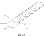
此效果是显示于图1,其是为以顶帽轮廓光束来镭射加工的信道的概要图。在图1中,通道10以具有顶帽或″圆形平面″轮廓的脉冲激光束(未显示)被镭射加工到基板12内。重迭的圆形14代表激光脉冲的位置。当以脉冲镭射将信道镭射加工时,基本上,当该镭射被脉冲化时,该镭射会被指引或沿着欲加工的信道路径平顺且连续地移动,从而将一平顺且连续的特征加工于基板中。真实数目的位置将依据镭射光点大小、期望的通道宽度与传送到基板的每一脉冲能量以及因每一脉冲移除的材料数量而改变。所示的脉冲位置数目会由真实实行大幅缩减,以更清楚显示这些位置。当脉冲光束向下转换该信道将跟随的预定路径时,所移除的材料数量是由来自每一点所接收的多个脉冲的通道中每一点上所接收的累积数量而计算。假如该镭射是连续波(CW)而非脉冲的话,所有这些实例将相等完整地应用。This effect is shown in Figure 1, which is a schematic diagram of a channel lasered with a top-hat profile beam. In FIG. 1 ,
图2显示藉由具有方形平面焦点的激光束而被镭射加工于基板22中的矩形截面通道20的图,其中一个显示为24。重迭的方形26,代表当信道20被加工时镭射焦点的连续位置。如图1,图标重迭镭射焦点位置的数目是概略的,并且其可以依据镭射重复率、激光脉冲能量、脉冲大小与其它脉冲参数而在实际操作时改变。要注意的是,因为镭射能量被均匀地分布在方形焦点上,所以当镭射光点沿着期望加工路径移动时,由信道中每一点所收到的计算累积剂量会相等,其是造成产生的通道拥有具有方形边缘的平面底部。这在LDA应用中常常令人期望。要注意的是,此分析是以脉冲与连续波镭射两者来进行。FIG. 2 shows a diagram of channels 20 of rectangular cross section, one of which is shown at 24 , laser machined in a substrate 22 by a laser beam having a square planar focus. The overlapping squares 26 represent the successive positions of the laser focus as the channel 20 is processed. As shown in Figure 1, the number of icon overlapping laser focus positions is approximate and may vary during actual operation depending on laser repetition rate, laser pulse energy, pulse size, and other pulse parameters. It should be noted that since the laser energy is evenly distributed over the square focus, the calculated cumulative dose received by each point in the channel will be equal as the laser spot moves along the desired processing path, which results in The channel has a flat bottom with square edges. This is often desirable in LDA applications. Note that this analysis was performed with both pulsed and continuous wave lasers.
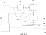
被设计来加工电子基板中的特定特征的镭射加工系统,例如在多层电子基板中的信道,其是已经在现有技术中被说明。美国专利申请案第5,798,927号,用于将在多阶段多重速率定位器系统中的阶段移动整合的装置与方法,发明人为Culter等人,其是被受让给本发明的受让人,其是说明结合具有高与低定位速率以及准确性的光束操纵装置,以快速且准确地定位激光束在工件上。美国专利申请案第6,433,301号,具有固态紫外光高斯光束的光束整型与投影成像以形成通道,发明人为Dunsky等人,其是说明使用绕射光学组件以形成用于通道钻孔应用的期望光束形状。图3显示现有技术镭射加工系统图,其是被设计以加工在多层电子基板中的信道。一种可能为脉冲化固态紫外光镭射的镭射30,在控制器32的指示下发出激光脉冲34,其是由可能为全像或绕射的光束塑型光学36所塑型,其随后在控制器32的指示下被可能多为阶段的光束操纵光学38操纵,至可能为平场聚焦透镜(f-theta)的扫瞄光学40,其后到可能为多层电子基板的工件42之上,该工件固定位置在动作控制单元44,该动作控制单元移动工件42与在控制器32指示下的激光脉冲34有关,且结合光束操纵光学36以造成激光脉冲34加工期望特征在工件42中。应用这些组件以加工特征于电子基板中的示范性系统,是为Si5330与ICP5650镭射加工处理系统,由奥勒冈州波特兰的电子科学工业与本发明受让人所制造。Laser processing systems designed to process specific features in electronic substrates, such as channels in multilayer electronic substrates, have been described in the prior art. U.S. Patent Application No. 5,798,927, Apparatus and Method for Integrating Phase Movements in a Multi-Stage Multi-Rate Locator System, inventors are Culter et al., which is assigned to the assignee of the present invention, which is Description Combines a beam steering device with high and low positioning rates and accuracy to quickly and accurately position a laser beam on a workpiece. U.S. Patent Application No. 6,433,301, Beam Shaping and Projection Imaging with Solid-State Ultraviolet Gaussian Beams to Form Channels, by Dunsky et al., describes the use of diffractive optical components to form desired beams for channel drilling applications shape. FIG. 3 shows a diagram of a prior art laser processing system designed to process channels in a multilayer electronic substrate. A
图4是为使用图3所说明的现有技术镭射加工系统来加工基板50中弯曲通道的结果的仿真。镭射加工处理系统(未显示)将一连串的方形平面激光脉冲52引导到基板50上,其是沿着路径57,起始于脉冲54并且结束于脉冲56。累积的镭射辐射剂量曲线58、62与66,以及因此在该点上所产生通道的截面,其是分别对应沿着线60、64与68的计算截面镭射辐射剂量。要注意的是,虽然截面58与66可令人接受,但是当激光脉冲52沿着路径57行进时,加工通道的形状则开始从方形侧边、平面底截面58偏离,直到它变为截面62,然后逐渐往回改变到截面66。这是不被期望的结果。从这些结果可证明,当加工发生时,现有技术系统藉由不适当地控制在该特征中每一点上累积的镭射辐射剂量而没有达到该加工通道的期望拓朴。FIG. 4 is a simulation of the results of processing a curved channel in a
随后需要的是为,当信道路径改变方向与形状时,一种在电子基板中达到具有与期望一致性尺寸与深度的镭射加工信道的方法与装置。What is then needed is a method and apparatus for achieving laser-machined channels in electronic substrates having dimensions and depths consistent with a desired size as the channel paths change direction and shape.
发明内容Contents of the invention
本发明的一种目的是为描述一种方法与装置,其是用于尽管特征路径方向与形状改变下,以一致性尺寸、深度与形状镭射加工于电子基板中的特征。本发明的另一种目的是为描述一种方法与装置,其是用于当特征被镭射加工时,尽管改变特征路径方向与形状,藉由实时改变焦点的形状以一致性尺寸、深度与形状镭射加工特征。It is an object of the present invention to describe a method and apparatus for laser machining features in electronic substrates of consistent size, depth and shape despite changes in feature path direction and shape. It is another object of the present invention to describe a method and apparatus for consistent size, depth and shape by changing the shape of the focal point in real time while the feature is being laser processed despite changing feature path direction and shape Laser processing features.
图5显示本发明的一种实施例,其是当激光脉冲加工一工件时,改变在进行中的激光脉冲焦点形状,并因而克服现有技术的上述缺点。期望的镭射焦点形状是依据被加工特征的形状来计算。已知欲被加工的被选定特定形状,当藉由期望特征外壳被移动及转动时,留下期望的平滑度与形状于该特征的侧边与底部,并且当镭射加工在激光脉冲与工件之间具有适当激光脉冲参数与相关运动参数时,维持期望的截面。FIG. 5 shows an embodiment of the present invention that changes the shape of the focal point of the laser pulse on the fly while the laser pulse is machining a workpiece, and thus overcomes the above-mentioned disadvantages of the prior art. The desired laser focus shape is calculated based on the shape of the feature being machined. It is known that the selected specific shape to be machined, when moved and rotated by the desired feature shell, leaves the desired smoothness and shape on the sides and bottom of the feature, and when the laser is processed between the laser pulse and the workpiece With appropriate laser pulse parameters and associated motion parameters in between, the desired cross-section is maintained.
图6显示可程序化光束塑型光学组件的更详细图标。本实施例将可程序化变形镜插入于镭射加工系统的光学路径中,当该系统加工于工件中的通道时,以允许该系统实时可程序化地改变该激光脉冲的焦点形状与能量分布。该实施例藉由接收激光脉冲、可选择地将该光束扩展出去并且将其投射到变形镜表面上来进行。该变形镜是由附着至可挠曲镜的致动器数组所组成。该镜子可被分段以允许致动器将附着其上的镜子部分不是个别就是连续地移动,其中该致动器可向上或向下地移动变形镜表面,即使其是为连续表面。我们选择连续模式以用于此实施例。藉由移动镜子表面,该镜子藉由引进相位移而将激光脉冲塑型,该些相位移会改变非常像全像的脉冲形状。将撞击镜子表面的镭射光校准,当它抵达镜子时以具有平面波前。被引入到变形镜表面的变化将相位移引入到波前,当聚焦到一光点时,该波前会产生藉由变形镜所引入的扰荡直接有关的镭射能量特别分布。自镜子反射的光线会被引导到光束操纵光学,然后扫瞄的透镜,以将该光点向下聚焦为一工作尺寸的光点。可选择地,自镜子反射的光线会被发送经过可选择的输出光学,在该情况下,变形镜距光束操纵与扫瞄光学一距离并且需要中继透镜以维持光束的特性。变形镜会被程序化,以反射激光脉冲信号的期望形状到扫瞄透镜,经由光束操纵光学与可选择的中继光学,从而在镜子分辨率内产生期望形状的激光脉冲焦点。Figure 6 shows a more detailed diagram of the programmable beam shaping optics. In this embodiment, a programmable deformable mirror is inserted into the optical path of the laser processing system to allow the system to programmatically change the focus shape and energy distribution of the laser pulse in real time when the system processes a channel in a workpiece. This embodiment works by receiving a laser pulse, optionally expanding the beam, and projecting it onto the deformable mirror surface. The deformable mirror consists of an array of actuators attached to a deflectable mirror. The mirror can be segmented to allow the actuator to move the mirror sections to which it is attached either individually or continuously, wherein the actuator can move up or down the deformable mirror surface even if it is a continuous surface. We choose continuous mode for this example. By moving the surface of the mirror, the mirror shapes the laser pulse by introducing phase shifts that alter the very hologram-like pulse shape. Laser light striking the mirror surface is collimated to have a flat wavefront when it reaches the mirror. The changes introduced to the surface of the deformable mirror introduce a phase shift into the wavefront which, when focused to a spot, produces a particular distribution of laser energy that is directly related to the perturbations introduced by the deformable mirror. Light reflected from the mirror is directed to the beam steering optics, which then scan the lens to focus the spot down to a working size spot. Alternatively, the light reflected from the mirror would be sent through an alternative output optic, in which case the deformable mirror is a distance from the beam steering and scanning optics and a relay lens is required to maintain the characteristics of the beam. The deformable mirror is programmed to reflect the desired shape of the laser pulse signal to the scan lens, via beam steering optics and optional relay optics, to produce the desired shape of the laser pulse focus within the resolution of the mirror.
因为变形镜改变激光脉冲波前,所以可能在镜子分辨率内产生具有任何灰阶密度的任何形状是可能的。这意味着,该系统可被程序化,以反射″灰阶″屏蔽,其中投射到基板上的镭射光的数量能被取值自该镭射焦点中任何点上输入光线的0%与100%之间。以此方式,该特征中个别点所接收的镭射辐射的累积剂量可被准确地程序化,其是使复杂的特征形状为可能的。其同样允许产生的焦点被转动,因为转动被程序化到变形镜内的图案,其是将会转动产生的焦点形状。Because the deformable mirror changes the laser pulse wavefront, it is possible to generate any shape with any grayscale density within the resolution of the mirror. This means that the system can be programmed to reflect "grayscale" masks, where the amount of laser light impinging on the substrate can be taken from between 0% and 100% of the incoming light at any point in the laser focus. between. In this way, the cumulative dose of laser radiation received by individual points in the feature can be accurately programmed, which makes complex feature shapes possible. It also allows the resulting focal point to be rotated, since the rotation is programmed into the pattern within the deformable mirror, which is the shape of the focal point that will be rotated.
此实施例使用事实,其为变形镜可被程序化且可在如100微秒的短时间将激光脉冲塑型为完成不同的形状。当该特征正被加工时,其使得变形镜改变正在进行中的激光脉冲焦点形状。计算被得到以决定需要多少不同的形状,以加工具有期望可允许偏差的特征,其来自名义上的形状,且在该些点上该些形状应该改变。该系统随后计算加工特征所需要的镭射参数,包括脉冲数目、镭射重复率、脉冲期与脉冲能量,并且随后将该镭射的脉冲化结合变形镜与光束操纵光学的更新,以镭射加工该特征。This embodiment uses the fact that deformable mirrors can be programmed and shape laser pulses to achieve different shapes in as short a time as 100 microseconds. When the feature is being machined, it causes the deformable mirror to change the shape of the focal point of the ongoing laser pulse. Calculations are made to determine how many different shapes are needed to machine a feature with the desired allowable deviation from the nominal shape at which points the shapes should change. The system then calculates the laser parameters required to process the feature, including number of pulses, laser repetition rate, pulse duration, and pulse energy, and then pulses the laser in combination with updates to the deformable mirror and beam steering optics to laser process the feature.
在操作特征时,其可能有一被镭射加工的信道的路径片段,其被检查以决定哪一或哪些镭射焦点形状将被使用来加工该特征。此信息可来自结合基板的CAD数据,并且随后被分析,以提取已知的路径片段,以搭配预定形状。一旦形状的顺序被选出,激光脉冲参数与动作控制参数则会被选出,以加工具有预期期望尺寸、形状与表面平滑度的特征。When manipulating a feature, there may be a path segment of the lasered channel that is examined to determine which laser focus shape or shapes will be used to machine the feature. This information can come from CAD data of the bonded substrate and then analyzed to extract known path segments to match the predetermined shape. Once the sequence of shapes is selected, the laser pulse parameters and motion control parameters are selected to machine features of the desired size, shape and surface smoothness.
镭射系统随后指示动作控制系统与激光脉冲操纵光学,以将基板移入与激光脉冲轴相关的位置并且开始产生激光脉冲。变形镜导致激光脉冲焦点将该些期望形状假定为动作控制系统,并且导致激光脉冲操纵光学结合,以改变与激光脉冲相关的基板位置。当镭射产生脉冲且基板相关于脉冲移动时,变形镜更新镭射焦点的形状,并因而导致激光脉冲加工具有期望的一致性拓朴的特征以及表面磨光,从而克服现有技术之前所描述的缺点。The laser system then instructs the motion control system and laser pulse steering optics to move the substrate into position relative to the laser pulse axis and initiates laser pulse generation. The deformable mirror causes the laser pulse focal point to assume these desired shapes as a motion control system and causes the laser pulse to manipulate the optical coupling to change the substrate position relative to the laser pulse. As the laser pulses and the substrate moves relative to the pulses, the deformable mirror updates the shape of the laser focus and thus results in laser pulse machining with the desired consistent topographical features and surface finish, thereby overcoming the previously described disadvantages of the prior art .
附图说明 Description of drawings
图1为显示具有圆形平面激光脉冲的现有技术镭射加工图。Figure 1 is a diagram showing prior art laser processing with circular planar laser pulses.
图2为显示具有方形平面激光脉冲的现有技术镭射加工图。Figure 2 is a diagram showing prior art laser processing with square planar laser pulses.
图3为现有技术镭射加工系统图。Fig. 3 is a diagram of a prior art laser processing system.
图4为藉由现有技术系统的基板中的弯曲特征加工图。4 is a diagram of curved feature processing in a substrate by a prior art system.
图5为根据本发明实施例来建构的镭射加工系统图。FIG. 5 is a diagram of a laser processing system constructed according to an embodiment of the present invention.
图6为根据本发明实施例来建构的可程序化光束塑型器图。Figure 6 is a diagram of a programmable beam shaper constructed in accordance with an embodiment of the present invention.
图7为藉由本发明实施例来镭射加工的弯曲特征图。FIG. 7 is a graph of bending features processed by laser processing according to an embodiment of the present invention.
图8为藉由本发明实施例来镭射加工的弯曲特征图。FIG. 8 is a graph of bending features processed by laser processing according to an embodiment of the present invention.
图9为藉由本发明实施例来镭射加工的弯曲特征图。FIG. 9 is a graph of bending features processed by laser processing according to an embodiment of the present invention.
具体实施方式 Detailed ways
诚如将在以下讨论所说明的,本发明实施例解决在该现有技术中所指出的问题,其是藉由将激光脉冲焦点塑型,以控制由激光脉冲传送到工件的能量的分布。图5显示本发明实施例,其具有可以为脉冲化、固态紫外光镭射的镭射70,其是在控制器72的指示下发射激光脉冲74,该激光脉冲是由准直光学76所塑型,其产生比从镭射70所发出的脉冲较大、准直的脉冲。准直光学76准直该些激光脉冲并将其扩展成期望的光束大小。在此点上,激光脉冲74具有数毫米的有效直径。激光脉冲74随后传送到焦点塑型光学77,其是在控制器72的指示下将激光脉冲焦点整型为期望的形状。该脉冲随后会被引导到脉冲操纵光学78,其是可为多阶段且同样地被控制器72所控制,然后到可以为平场聚焦透镜的扫瞄光学80上,该扫瞄光学聚焦并且引导激光脉冲74到可以为电子基板的工件82上,该工件是被固定位置在动作控制组件84上,该组件在控制器72指示下相关于激光脉冲74移动工件82,并且结合光束操纵光学78,以造成激光脉冲74被引导到工件82上的期望点,从而加工在工件82中的期望特征。As will be explained in the following discussion, embodiments of the present invention address the problems identified in this prior art by controlling the distribution of energy delivered by the laser pulses to the workpiece by shaping the focus of the laser pulses. Figure 5 shows an embodiment of the invention having a
图6显示焦点整型光学77的细节。激光脉冲74是由可选择的输入光学90所接收,在此如果需要的话,准直脉冲会被放大并且被投射在具有大约9.6mm清楚孔隙的变形镜92的表面上。在控制器(未显示)的控制之下,变形镜会在将激光脉冲74反射到可选择输出光学94以前将它们调整与塑型,输出光学94传递激光脉冲到脉冲操纵光学78上。在镜子92与脉冲操纵光学78被分隔超过数公分的情形中,输出光学94被使用来传递变形镜92的输出。变形镜92可藉由将致动器数组中的每一致动器附着到单一可挠性镜的背部来建构。当致动器向上与向下移动时,它们会将镜子表面变形。致动器的分辨率使得此种变形镜藉由于激光束波前中产生可程序移位而能够与激光脉冲相互作用,从而产生像全像的干涉形态于激光脉冲中,其中该些波的建构性与破坏性干涉会使镭射焦点塑型。一种使镜子程序化的可能方法是为计算与所期望焦点形状的傅力叶转换的实数、正数部分成比例的一连串系数,以及使用它们来程序化该镜子。FIG. 6 shows details of
示范性变形镜组件是为由麻萨诸塞州剑桥波士顿微机械公司所制造的Kilo-DM。此装置包含具有32×32镜子组件数组,每一镜子组件具有达到1.5微动行程、9.6毫米清楚孔隙。此装置可以到达10千赫兹的框速率来更新整个数组,其意味着激光脉冲焦点可在100微秒内完全改变。An exemplary deformable mirror assembly is the Kilo-DM manufactured by Boston Micromechanics in Cambridge, MA. The device includes an array of 32 x 32 mirror assemblies, each mirror assembly has a fine movement stroke of 1.5 mm and a clear aperture of 9.6 mm. The device can reach a frame rate of 10 kilohertz to update the entire array, which means that the laser pulse focus can be completely changed within 100 microseconds.
图7是为使用图5所说明的本发明实施例将基板100中的弯曲通道加工的仿真结果。镭射加工系统(未显示)引导一系列的塑型激光脉冲,其是具有到基板100的基本激光脉冲焦点形状101,其是如需要地转动该基本形状,以配合该信道的曲线。脉冲102会被引导到基板100,其是沿着路径107在脉冲104开始并在脉冲106结束。累积的镭射辐射剂量曲线108、112与116以及在该点上因此产生的通道的截面,其是分别对应沿着线计算的截面镭射辐射剂量110、114与118。要注意的是,所有截面108、112与116皆是令人可接受的期望结果,其是意味着产生的通道将具有方形侧边、平坦底部的截面于其整个长度。FIG. 7 is a simulation result of machining a curved channel in
图8是为本发明另一实施例的模拟情形。镭射加工系统(未显示)引导具有基本镭射焦点形状121的一连串塑型激光脉冲。要注意的是,焦点形状已经被程序化,以具有修改的强度分布穿过焦点。在镭射焦点形状121上的截面线122具有强度分布,以及因此的镭射辐射剂量124。就与线122平行的所有截面而言,强度分布是相同的。以与截面122直角取得的截面线126,其是显示强度128穿过焦点形状的均匀分布。此修改的镭射能量分布允许此形状加工具有矩形截面的特征。该实施例藉由当被选择的焦点形状转动且沿着路径转换时,计算该累积剂量并且将该能量分布的轮廓划成焦点形状而得到此结果,以致于在每一点上的累积能量剂量相等。图8显示该修改的焦点形状如何使用于加工基板中的特征。其中之一标示为132的该些激光脉冲焦点形状,被引导到基板130上,沿着路径137在脉冲134开始,且在脉冲136结束。累积镭射辐射剂量曲线144、146与148以及在那点上因此产生通道的截面,其是分别对应沿着线计算的截面镭射辐射剂量138、140与142。要注意的是,所有截面144、146与148是为可接受的期望结果,其是意味着产生的通道将具有方形侧边、平坦底部的截面于其整个长度。FIG. 8 is a simulated situation of another embodiment of the present invention. A laser machining system (not shown) directs a series of shaping laser pulses having a basic laser focus shape 121 . Note that the focal shape has been programmed to have a modified intensity distribution across the focal point. A section line 122 on the laser focus shape 121 has an intensity distribution, and thus a laser radiation dose 124 . The intensity distribution is the same for all sections parallel to line 122 . Section line 126 , taken at right angles to section 122 , shows a uniform distribution of intensity 128 across the focal shape. This modified laser energy distribution allows this shape to machine features with rectangular cross-sections. This embodiment achieves this by calculating the cumulative dose and contouring the energy distribution to the focal shape as the selected focal shape rotates and transitions along the path such that the cumulative energy dose at each point is equal . Figure 8 shows how this modified focal shape can be used to process features in a substrate. One of the laser pulse focal shapes, designated 132 , is directed onto a substrate 130 along a path 137 beginning at pulse 134 and ending at pulse 136 . The cumulative laser dose curves 144, 146 and 148 and thus the cross-sections of the channel at that point are corresponding to the cross-sectional laser doses 138, 140 and 142 calculated along the lines, respectively. Note that all cross-sections 144, 146 and 148 are acceptable desired results, which means that the resulting channel will have square-sided, flat-bottomed cross-sections throughout its length.
图9显示来自本发明另一实施例的结果。在图9中,基板150被具有紧沿着期望特征轮廓(未显示)的边缘的激光脉冲焦点形状151镭射加工。此镭射焦点形状151将被转动与转换,沿着开始于位置154且在156结束的路径157。其中之一标示为152的该些激光脉冲焦点将被转换与转动,以适合期望路径157。累积的镭射辐射剂量曲线158、160与162以及在那点上因此产生通道的截面,其是会分别对应沿着线计算的截面镭射辐射剂量164、166与168。要注意的是,所有截面158、160与162均为可接受的期望结果,其是意味着产生的通道将具有方形侧边、平坦底部的截面于其整个长度。Figure 9 shows results from another embodiment of the invention. In FIG. 9, a
该技术领域中具有通常知识者将会理解到,在不背离根本原理之下,可对上述本发明实施例的细节进行许多改变。本发明的范畴应该因此仅由该申请专利范围所决定。Those skilled in the art will appreciate that many changes may be made to the details of the above-described embodiments of the invention without departing from the underlying principles. The scope of the invention should therefore only be determined by the scope of this application.
Claims (6)
Applications Claiming Priority (3)
| Application Number | Priority Date | Filing Date | Title |
|---|---|---|---|
| US12/413,531 | 2009-03-28 | ||
| US12/413,531 US8350187B2 (en) | 2009-03-28 | 2009-03-28 | Method and apparatus for laser machining |
| PCT/US2010/028884 WO2010117683A2 (en) | 2009-03-28 | 2010-03-26 | Improved method and apparatus for laser machining |
Publications (1)
| Publication Number | Publication Date |
|---|---|
| CN102405122A true CN102405122A (en) | 2012-04-04 |
Family
ID=42782835
Family Applications (1)
| Application Number | Title | Priority Date | Filing Date |
|---|---|---|---|
| CN2010800174075A Pending CN102405122A (en) | 2009-03-28 | 2010-03-26 | Improved method and apparatus for laser machining |
Country Status (6)
| Country | Link |
|---|---|
| US (1) | US8350187B2 (en) |
| JP (1) | JP2012521890A (en) |
| KR (1) | KR20120004426A (en) |
| CN (1) | CN102405122A (en) |
| TW (1) | TW201043373A (en) |
| WO (1) | WO2010117683A2 (en) |
Cited By (1)
| Publication number | Priority date | Publication date | Assignee | Title |
|---|---|---|---|---|
| CN114654082A (en) * | 2016-12-30 | 2022-06-24 | 伊雷克托科学工业股份有限公司 | Method and system for extending the life of optics in laser processing equipment |
Families Citing this family (10)
| Publication number | Priority date | Publication date | Assignee | Title |
|---|---|---|---|---|
| US9346130B2 (en) | 2008-12-17 | 2016-05-24 | Electro Scientific Industries, Inc. | Method for laser processing glass with a chamfered edge |
| US10357850B2 (en) | 2012-09-24 | 2019-07-23 | Electro Scientific Industries, Inc. | Method and apparatus for machining a workpiece |
| US9828278B2 (en) | 2012-02-28 | 2017-11-28 | Electro Scientific Industries, Inc. | Method and apparatus for separation of strengthened glass and articles produced thereby |
| US9828277B2 (en) * | 2012-02-28 | 2017-11-28 | Electro Scientific Industries, Inc. | Methods for separation of strengthened glass |
| JP2015516352A (en) | 2012-02-29 | 2015-06-11 | エレクトロ サイエンティフィック インダストリーズ インコーポレーテッド | Method and apparatus for processing tempered glass and products produced thereby |
| WO2014038241A1 (en) * | 2012-09-05 | 2014-03-13 | 三菱電機株式会社 | Laser processing device |
| US10478918B2 (en) | 2014-11-20 | 2019-11-19 | Zeon Corporation | Method for manufacturing optical film |
| US20190202005A1 (en) | 2016-04-28 | 2019-07-04 | Zeon Corporation | Method for manufacturing optical film |
| TWI773067B (en) * | 2021-01-04 | 2022-08-01 | 財團法人工業技術研究院 | Adjustment method of laser light path and adjustment device of laser light path |
| EP4169654A1 (en) * | 2021-10-25 | 2023-04-26 | Bystronic Laser AG | Determination of transition phases for transforming different dynamic laser beam shapes for a laser cutting machine |
Citations (4)
| Publication number | Priority date | Publication date | Assignee | Title |
|---|---|---|---|---|
| JPH05261578A (en) * | 1992-01-13 | 1993-10-12 | Maho Ag | Process and device for machining workpiece by means of laser radiation emitted from laser |
| JPH10263872A (en) * | 1997-03-24 | 1998-10-06 | Komatsu Ltd | Laser processing machine |
| US20020158052A1 (en) * | 2001-03-29 | 2002-10-31 | Ehrmann Jonathan S. | Method and system for processing one or more microstructures of a multi-material device |
| WO2007044798A2 (en) * | 2005-10-11 | 2007-04-19 | Gsi Group Corporation | Optical metrological scale and laser-based manufacturing method therefor |
Family Cites Families (19)
| Publication number | Priority date | Publication date | Assignee | Title |
|---|---|---|---|---|
| US4417393A (en) * | 1981-04-01 | 1983-11-29 | General Electric Company | Method of fabricating high density electronic circuits having very narrow conductors |
| US4487993A (en) * | 1981-04-01 | 1984-12-11 | General Electric Company | High density electronic circuits having very narrow conductors |
| GB8414178D0 (en) * | 1984-06-04 | 1984-07-11 | Soszek P | Circuitry |
| EP0262225A4 (en) * | 1986-03-26 | 1988-12-12 | Ni Ts Tekh Lazeram An | Installation for laser treatment of materials. |
| JPS6384788A (en) * | 1986-09-29 | 1988-04-15 | Nippon Steel Corp | Method and device for controlling projection of laser beam |
| DE4404141A1 (en) * | 1994-02-09 | 1995-08-10 | Fraunhofer Ges Forschung | Device and method for laser beam shaping, especially in laser beam surface processing |
| DE4417245A1 (en) * | 1994-04-23 | 1995-10-26 | Lpkf Cad Cam Systeme Gmbh | High resolution structured metallisation prodn. |
| US5751585A (en) * | 1995-03-20 | 1998-05-12 | Electro Scientific Industries, Inc. | High speed, high accuracy multi-stage tool positioning system |
| US6046429A (en) * | 1997-06-12 | 2000-04-04 | International Business Machines Corporation | Laser repair process for printed wiring boards |
| US6163957A (en) * | 1998-11-13 | 2000-12-26 | Fujitsu Limited | Multilayer laminated substrates with high density interconnects and methods of making the same |
| TW482705B (en) * | 1999-05-28 | 2002-04-11 | Electro Scient Ind Inc | Beam shaping and projection imaging with solid state UV Gaussian beam to form blind vias |
| US6143356A (en) * | 1999-08-06 | 2000-11-07 | Parelec, Inc. | Diffusion barrier and adhesive for PARMOD™ application to rigid printed wiring boards |
| DE19959921C1 (en) * | 1999-12-11 | 2001-10-18 | Schott Spezialglas Gmbh | Method and device for cutting flat workpieces made of brittle material |
| DE19963939B4 (en) * | 1999-12-31 | 2004-11-04 | Schott Spezialglas Gmbh | Method and device for cutting flat workpieces made of brittle material |
| JP4014498B2 (en) * | 2002-12-17 | 2007-11-28 | 日立ビアメカニクス株式会社 | Multi-axis laser processing machine |
| US6909735B2 (en) * | 2003-04-10 | 2005-06-21 | Hitachi Via Mechanics, Ltd. | System and method for generating and controlling multiple independently steerable laser beam for material processing |
| US7014727B2 (en) * | 2003-07-07 | 2006-03-21 | Potomac Photonics, Inc. | Method of forming high resolution electronic circuits on a substrate |
| US7511247B2 (en) * | 2004-03-22 | 2009-03-31 | Panasonic Corporation | Method of controlling hole shape during ultrafast laser machining by manipulating beam polarization |
| JP2006007257A (en) * | 2004-06-24 | 2006-01-12 | Matsushita Electric Ind Co Ltd | Laser processing equipment |
-
2009
- 2009-03-28 US US12/413,531 patent/US8350187B2/en not_active Expired - Fee Related
-
2010
- 2010-03-26 JP JP2012502298A patent/JP2012521890A/en not_active Ceased
- 2010-03-26 CN CN2010800174075A patent/CN102405122A/en active Pending
- 2010-03-26 TW TW099109058A patent/TW201043373A/en unknown
- 2010-03-26 KR KR1020117022685A patent/KR20120004426A/en not_active Withdrawn
- 2010-03-26 WO PCT/US2010/028884 patent/WO2010117683A2/en not_active Ceased
Patent Citations (4)
| Publication number | Priority date | Publication date | Assignee | Title |
|---|---|---|---|---|
| JPH05261578A (en) * | 1992-01-13 | 1993-10-12 | Maho Ag | Process and device for machining workpiece by means of laser radiation emitted from laser |
| JPH10263872A (en) * | 1997-03-24 | 1998-10-06 | Komatsu Ltd | Laser processing machine |
| US20020158052A1 (en) * | 2001-03-29 | 2002-10-31 | Ehrmann Jonathan S. | Method and system for processing one or more microstructures of a multi-material device |
| WO2007044798A2 (en) * | 2005-10-11 | 2007-04-19 | Gsi Group Corporation | Optical metrological scale and laser-based manufacturing method therefor |
Cited By (1)
| Publication number | Priority date | Publication date | Assignee | Title |
|---|---|---|---|---|
| CN114654082A (en) * | 2016-12-30 | 2022-06-24 | 伊雷克托科学工业股份有限公司 | Method and system for extending the life of optics in laser processing equipment |
Also Published As
| Publication number | Publication date |
|---|---|
| KR20120004426A (en) | 2012-01-12 |
| WO2010117683A3 (en) | 2011-01-13 |
| US8350187B2 (en) | 2013-01-08 |
| TW201043373A (en) | 2010-12-16 |
| JP2012521890A (en) | 2012-09-20 |
| WO2010117683A2 (en) | 2010-10-14 |
| US20100243626A1 (en) | 2010-09-30 |
Similar Documents
| Publication | Publication Date | Title |
|---|---|---|
| CN102405122A (en) | Improved method and apparatus for laser machining | |
| JP4551086B2 (en) | Partial machining with laser | |
| JP4057311B2 (en) | Electronic control of light spot | |
| KR101270333B1 (en) | Beam splitter and dynamic beam splitting method | |
| CN105121088B (en) | Laser processing apparatus and method of processing workpieces via laser tool manipulation | |
| TWI504463B (en) | Method and apparatus for controlling the size of a laser beam focal spot | |
| CN102271858A (en) | Method and apparatus for forming grooves in the surface of a polymer layer | |
| KR102327735B1 (en) | Laser apparatus and method of manufacturing the same | |
| JP2004528991A5 (en) | ||
| KR20150005939A (en) | Method and device for machining a workpiece using laser radiation | |
| CN105163897A (en) | Coordination of beam angle and workpiece movement for taper control | |
| JP2004526575A (en) | Ultraviolet laser ablation patterning method of fine structure in semiconductor | |
| KR20190025721A (en) | Laser processing apparatus and method for laser processing a workpiece | |
| US20100272959A1 (en) | Method and unit for micro-structuring a moving substrate | |
| CN111432976B (en) | Device for 3D shaping of a workpiece by means of a fluid jet guided laser beam | |
| KR20170096415A (en) | Laser cleaning method and laser processing method and apparatus using the laser cleaning method | |
| TW202231393A (en) | Laser processing apparatus, methods of operating the same, and methods of processing workpieces using the same | |
| JP2008168297A (en) | Apparatus and method for laser beam machining | |
| CN106624353A (en) | Laser shotblast product surface fabrication system | |
| JP2008137058A (en) | Laser beam machining apparatus and method | |
| KR20190056895A (en) | Micro Pattern Processing Apparatus Using Laser | |
| EP4512567A1 (en) | A system for forming a three-dimensional cavity and a method for forming a three-dimensional cavity | |
| EP4353690A1 (en) | System and method for processing a transparent material | |
| KR20240169542A (en) | Method and apparatus for ablating holes in an article | |
| KR20240169541A (en) | Method and apparatus for ablating holes in an article |
Legal Events
| Date | Code | Title | Description |
|---|---|---|---|
| C06 | Publication | ||
| PB01 | Publication | ||
| C10 | Entry into substantive examination | ||
| SE01 | Entry into force of request for substantive examination | ||
| C02 | Deemed withdrawal of patent application after publication (patent law 2001) | ||
| WD01 | Invention patent application deemed withdrawn after publication |
Application publication date: 20120404 |