CN102324432A - Organic electroluminescent device with inclined separation zone and coating manufacturing technology - Google Patents
Organic electroluminescent device with inclined separation zone and coating manufacturing technology Download PDFInfo
- Publication number
- CN102324432A CN102324432A CN2011101561052A CN201110156105A CN102324432A CN 102324432 A CN102324432 A CN 102324432A CN 2011101561052 A CN2011101561052 A CN 2011101561052A CN 201110156105 A CN201110156105 A CN 201110156105A CN 102324432 A CN102324432 A CN 102324432A
- Authority
- CN
- China
- Prior art keywords
- pixel
- longitudinal subdivision
- organic
- subdivision band
- electroluminescence device
- Prior art date
- Legal status (The legal status is an assumption and is not a legal conclusion. Google has not performed a legal analysis and makes no representation as to the accuracy of the status listed.)
- Granted
Links
Images


Classifications
-
- H—ELECTRICITY
- H10—SEMICONDUCTOR DEVICES; ELECTRIC SOLID-STATE DEVICES NOT OTHERWISE PROVIDED FOR
- H10K—ORGANIC ELECTRIC SOLID-STATE DEVICES
- H10K59/00—Integrated devices, or assemblies of multiple devices, comprising at least one organic light-emitting element covered by group H10K50/00
- H10K59/30—Devices specially adapted for multicolour light emission
- H10K59/35—Devices specially adapted for multicolour light emission comprising red-green-blue [RGB] subpixels
- H10K59/353—Devices specially adapted for multicolour light emission comprising red-green-blue [RGB] subpixels characterised by the geometrical arrangement of the RGB subpixels
-
- H—ELECTRICITY
- H05—ELECTRIC TECHNIQUES NOT OTHERWISE PROVIDED FOR
- H05B—ELECTRIC HEATING; ELECTRIC LIGHT SOURCES NOT OTHERWISE PROVIDED FOR; CIRCUIT ARRANGEMENTS FOR ELECTRIC LIGHT SOURCES, IN GENERAL
- H05B33/00—Electroluminescent light sources
- H05B33/10—Apparatus or processes specially adapted to the manufacture of electroluminescent light sources
-
- H—ELECTRICITY
- H10—SEMICONDUCTOR DEVICES; ELECTRIC SOLID-STATE DEVICES NOT OTHERWISE PROVIDED FOR
- H10K—ORGANIC ELECTRIC SOLID-STATE DEVICES
- H10K59/00—Integrated devices, or assemblies of multiple devices, comprising at least one organic light-emitting element covered by group H10K50/00
- H10K59/10—OLED displays
- H10K59/12—Active-matrix OLED [AMOLED] displays
- H10K59/122—Pixel-defining structures or layers, e.g. banks
-
- H—ELECTRICITY
- H10—SEMICONDUCTOR DEVICES; ELECTRIC SOLID-STATE DEVICES NOT OTHERWISE PROVIDED FOR
- H10K—ORGANIC ELECTRIC SOLID-STATE DEVICES
- H10K71/00—Manufacture or treatment specially adapted for the organic devices covered by this subclass
- H10K71/10—Deposition of organic active material
- H10K71/12—Deposition of organic active material using liquid deposition, e.g. spin coating
- H10K71/13—Deposition of organic active material using liquid deposition, e.g. spin coating using printing techniques, e.g. ink-jet printing or screen printing
- H10K71/135—Deposition of organic active material using liquid deposition, e.g. spin coating using printing techniques, e.g. ink-jet printing or screen printing using ink-jet printing
-
- H—ELECTRICITY
- H10—SEMICONDUCTOR DEVICES; ELECTRIC SOLID-STATE DEVICES NOT OTHERWISE PROVIDED FOR
- H10K—ORGANIC ELECTRIC SOLID-STATE DEVICES
- H10K2102/00—Constructional details relating to the organic devices covered by this subclass
- H10K2102/301—Details of OLEDs
- H10K2102/351—Thickness
-
- H—ELECTRICITY
- H10—SEMICONDUCTOR DEVICES; ELECTRIC SOLID-STATE DEVICES NOT OTHERWISE PROVIDED FOR
- H10K—ORGANIC ELECTRIC SOLID-STATE DEVICES
- H10K59/00—Integrated devices, or assemblies of multiple devices, comprising at least one organic light-emitting element covered by group H10K50/00
- H10K59/10—OLED displays
- H10K59/17—Passive-matrix OLED displays
- H10K59/173—Passive-matrix OLED displays comprising banks or shadow masks
Landscapes
- Engineering & Computer Science (AREA)
- Manufacturing & Machinery (AREA)
- Microelectronics & Electronic Packaging (AREA)
- Electroluminescent Light Sources (AREA)
Abstract
Organic electroluminescent devices with slanted banks and coating fabrication techniques. The invention discloses an organic electroluminescent device, comprising: a transparent substrate having at least first, second and third pixels defined thereon; a first longitudinal bank located between the first pixel and the second pixel; a second longitudinal division strip located between the second pixel and the third pixel; and an organic luminous polymer layer on the substrate between the first longitudinal division strip and the second longitudinal division strip. The device further includes a transverse bank extending between the first longitudinal bank and the second longitudinal bank. The side walls of the longitudinal and transverse banks are inclined outwardly. The transverse banks have a height less than the longitudinal banks. The method of making the device uses nozzle coating or ink jet coating and uses a specially configured mask for creating banks of different heights.
Description
The application is that the original bill application number is dividing an application of 200310103813.5 application for a patent for invention (applying date: on November 06th, 2003, denomination of invention: have the organic electroluminescence device of inclination dividing strip and apply manufacturing technology).
Technical field
The present invention relates to display of organic electroluminescence, more particularly, the present invention relates to the method that a kind of utilization inclination dividing strip (sloped banks) and nozzle paint-on technique or ink-jet paint-on technique are made display of organic electroluminescence.
Background technology
Display of organic electroluminescence comprises: negative electrode is used to inject electronics; Anode is used for injected hole; And organic electro luminescent layer, between these two electrodes.That is, between anode and negative electrode, organic electroluminescent LED has the organic film of sandwich construction.When forward current is applied to organic electroluminescent LED,, electron-hole pair (is commonly referred to: exciton) combine because the anode in hole is provided and the P-N between the negative electrode of electronics is provided knot.Energy when the energy when electron-hole pair is combined separates than them is low.Organic electroluminescence cell is transformed to light to combination electronics-hole pair and energy gap between the electron-hole pair that separates.That is, when electric current flow through, organic electro luminescent layer was sent because electric current electronics and hole reconfigures together and the energy that produces when flowing.
According to above principle, to compare with LCD, organic electroluminescence device does not need additional source of light.In addition, the thin thickness of electroluminescent device, in light weight, and also energy efficiency is high.Organic electroluminescence device has the very favorable condition that is used for display image, and is for example, low in energy consumption, brightness is high, the response time is short and in light weight.Because have these advantage, so organic electroluminescence device is applicable to various electronics, mobile communication equipment for example, PDA (personal digital assistant), camcorders and hand held PC.Because the manufacture process when making organic electroluminescence device is simple,, reduced production cost so compare with LCD.
The driving method of operation display of organic electroluminescence is divided into passive matrix and active array type.Compare with active array type, the simple in structure and manufacture process of passive matrix is simple, but power consumption is high.In addition, passive matrix is difficult to make large-sized display of organic electroluminescence, and along with the increase of bus number, the aperture is than reducing.
On the contrary, compare with passive matrix, the brightness of active matrix type organic electroluminescent device is high, display quality is high.The core parts of organic electroluminescence device are organic electroluminescent (EL) materials, for example low or HMW organic EL Material.Handle the HMW organic EL Material easily, and be difficult to handle the low-molecular-weight organic EL Material, and the HMW organic EL Material has good thermal endurance.
Fig. 1 is the schematic sectional view that illustrates according to the active matrix type organic electroluminescent display of background technology.
As shown in Figure 1, display of organic electroluminescence 10 comprises first substrate 12 and second substrate 28 that utilizes sealant 26 to link together.On first substrate 12, form a plurality of thin-film transistors (TFT) T and array portion 14.Order forms first electrode (that is anode) 16, organic luminous layer 18 and second electrode (that is negative electrode) 20 on TFT T and array portion 14.At this moment, at each pixel P, organic luminous layer 18 comprises red (R), green (G) or blue (B), and therefore, each pixel P sends red (R) light, green (G) light or indigo plant (B) light.That is,, in each pixel P, be respectively arranged with machine colorful light-emitting figure for color display.In addition, through composition or printing color organic material in each pixel P, form organic luminous layer 18.
Still with reference to figure 1, second substrate 28 that utilizes sealant 26 to be connected to first substrate 12 comprises the hygroscopic agent 22 that is positioned on its back side.The moisture that hygroscopic agent 22 absorbs in the cell gap that possibly be present between first substrate 12 and second substrate 28.If hygroscopic agent 22 is arranged on second substrate 28, then etching part second substrate 28 is to form groove.After this, powder-type hygroscopic agent 22 is arranged in this groove, then, band 25 is adhered on second substrate 28 so that powder-type hygroscopic agent 22 is fixed in this groove.
In said structure and configuration, for example utilizing, the nozzle paint-on technique forms organic luminous layer.In the nozzle paint-on technique, utilize dividing plate (separator) or dividing strip (banks) to form independent red (R), green (G) and blue (B) organic luminous layer.If the major axis of pixel is defined as vertically, and the minor axis of pixel is defined as laterally, then nozzle longitudinally moves with straight line, reciprocating manner, thereby forms the color organic EL material, and therefore, organic luminous layer is to have the rectilinear form of hoping width.Therefore, each pixel of arranging in the vertical has same colored EL material each other, so send the light of same color.In addition, be arranged in each horizontal pixel and alternately have red (R) look, green (G) look and indigo plant (B) look.At this moment; Disturb in order to prevent between red (R) and green (G) EL material, green (G) and blue (B) EL material or indigo plant (B) and red (R) EL material, to produce; Between red (R) organic luminous layer, green (G) organic luminous layer and indigo plant (B) organic luminous layer, the longitudinal subdivision band is being set vertically.
For example utilize photoetching process or printing process, can form the longitudinal subdivision band.If utilize photoetching process to form the longitudinal subdivision band, then at first utilize spin coating method or spraying method on this substrate, to form organic material, then, deposit photoresist on organic material.After this, its shape is set and is used for exposure on photoresist corresponding to the mask of longitudinal subdivision band.After utilizing mask exposure, the photoresist that development is made public is so that it has the dividing strip shape.Then, organic material is etched to the longitudinal subdivision band.
Fig. 2 illustrates the floor map that has the organic electroluminescence device of longitudinal subdivision band according to background technology.As shown in the figure, a plurality of longitudinal subdivision bands 50 vertically are being set.A plurality of pixels 60 are set between longitudinal subdivision band 50.In each pixel 60, thin-film transistor T and pixel electrode 57 are set.When between two longitudinal subdivision bands 50, forming color organic light emitting layer 62, the nozzle that is used to inject organic EL Material is vertically moving, and then, organic EL Material is coated on the substrate.At this moment, be very difficult to make color organic light emitting layer 62 to have even, stable thickness, because during nozzle moves, the sweep speed of nozzle is very different with the quantity for spray of organic EL Material and be variable.
Fig. 3 illustrates the perspective illustration that between the longitudinal subdivision band, on substrate, forms the nozzle injection process of light emitting polymer according to background technology.On substrate 100, form a plurality of pixels 60, and on substrate, a plurality of longitudinal subdivision bands 50 are being set vertically, divide each pixel 60 of vertically arranging simultaneously.Nozzle 80 is injected light emitting polymer 90 between longitudinal subdivision band 50.When after nozzle injection, making light emitting polymer 90 planarizations, the light emitting polymer 90 of injection can be from the edge end, substrate 100 of the groove between two longitudinal subdivision bands 50 to dirty.Therefore, the thickness attenuation of the light emitting polymer 90 of injection, and be very difficult to make luminescent layer 90 planarizations.In addition, between each the longitudinal subdivision band 50 on the substrate 100, luminescent layer 90 in uneven thickness, and change.
In order to address these problems, to reduce the sweep speed of nozzle 80 sometimes.Yet, reduce sweep speed and can cause overflowing from the longitudinal subdivision band, make light emitting polymer 90 influence the light emitting polymer of neighbor.If improve the sweep speed of nozzle 80, then can in the groove between two longitudinal subdivision bands 50, form luminescent layer 90, but maybe be extremely thin.The operating characteristic of the organic electroluminescence device of therefore, being accomplished is bad.
In addition, the shape of longitudinal subdivision band 50 also influences the thickness and the planarization of luminescent layer 90.Fig. 4 is the cutaway view of getting along the line IV-IV among Fig. 3.As shown in Figure 4, longitudinal subdivision band 50 has rectangular section.Like this, because the surface tension of liquid phase light emitting polymer 90, so the contact portion S between light emitting polymer 90 and longitudinal subdivision band 50, light emitting polymer 90 against longitudinal subdivision band 50 raises.Therefore, the thickness of light emitting polymer 90 is regional thick contact longitudinal subdivision band 50, and the planarization situation is poor.Therefore, the inhomogeneities of luminescent layer 90 thickness makes that with unevennessization the luminosity of organic electroluminescence device is low, and efficient is low.In addition, also shortened the life-span of luminescent layer 90.
Summary of the invention
Therefore, the present invention relates to a kind of the solution basically because one or more problem of the limitation of background technology and defective generation, be used to make the method for display of organic electroluminescence.
An object of the present invention is to provide a kind ofly in the nozzle coating procedure, can make light emitting polymer have even flatness and thickness, be used to make the method for display of organic electroluminescence.
In following explanation, other features and advantages of the present invention will be described, and partly pass through that it is more obvious that other features and advantages of the present invention will become, perhaps through realizing that the present invention can learn other features and advantages of the present invention according to following explanation.Utilize the structure that particularly points out in printed instructions and claim thereof and the accompanying drawing, can realize and obtain the object of the invention and other advantages.
In order to realize these and other advantage; And according to the object of the invention; As this realize and broadly described, the method for making organic electroluminescence device comprises: define above that and form first electrode on the transparency carrier of a plurality of first, second and the 3rd pixels; Utilize mask; On first electrode, form a plurality of longitudinal subdivision bands and horizontal dividing strip; Wherein along the major axis of pixel the longitudinal subdivision band is being set vertically along the border of neighbor; And the longitudinal subdivision band has sloped sidewall, and wherein along the border of neighbor at the horizontal dividing strip of horizontally set along the minor axis of pixel, and laterally dividing strip has different height and width; Between each longitudinal subdivision band, form organic light-emitting polymer layer on first electrode in a plurality of first, second and the 3rd pixels, the organic luminescence polymer layer sends ruddiness, green glow and blue light respectively; And on the organic luminescence polymer layer, form second electrode, second electrode be separately positioned on each first, second and the 3rd pixel in.
In one aspect of the method, the method for making organic electroluminescence device comprises: on transparency carrier, limit a plurality of first, second and the 3rd pixels; On transparency carrier, form a plurality of thin-film transistors, each thin-film transistor corresponds respectively to each in a plurality of first, second and the 3rd pixels, and each thin-film transistor comprises grid, active layer, source electrode and drain electrode; On whole base plate, form passivation layer to cover a plurality of thin-film transistors, passivation layer has a plurality of drain contact holes that expose drain electrode respectively; Form first electrode respectively on the passivation layer in first, second and the 3rd pixel each, first electrode is through drain contact hole contact drain electrode; Utilize mask; On first electrode, form a plurality of longitudinal subdivision bands and horizontal dividing strip; Wherein along the major axis of pixel the longitudinal subdivision band is being set vertically along the border of neighbor; And the longitudinal subdivision band has sloped sidewall, and wherein along the border of neighbor at the horizontal dividing strip of horizontally set along the minor axis of pixel, and laterally dividing strip has different height and width; Between each longitudinal subdivision band, on first electrode on a plurality of first, second and the 3rd pixels, form organic light-emitting polymer layer, the organic luminescence polymer layer sends ruddiness, green glow and blue light respectively; And on the organic luminescence polymer layer, form second electrode, second electrode be separately positioned on each first, second and the 3rd pixel in.
Obviously, more than to general remark that the present invention did and following all be typicalness and illustrative to the detailed description that the present invention did, and be intended to further construe and require described the present invention.
Description of drawings
Included accompanying drawing helps further to understand the present invention, and introduces the part of this specification as this specification, and it illustrates the embodiment of the invention and is used to explain the principle of the invention with explanation.Accompanying drawing comprises:
Fig. 1 is the schematic sectional view that illustrates according to the active matrix type organic electroluminescent display of background technology;
Fig. 2 illustrates the floor map that has the organic electroluminescence device of longitudinal subdivision band according to background technology;
Fig. 3 illustrates the perspective illustration that between the longitudinal subdivision band, on substrate, forms the nozzle injection process of light emitting polymer according to background technology;
Fig. 4 is the cutaway view of getting along the line IV-IV among Fig. 3;
Fig. 5 illustrates the perspective illustration that has the longitudinal subdivision band and the substrate of horizontal dividing strip according to the present invention;
Fig. 6 A to 6C is according to the cutaway view of longitudinal subdivision band of the present invention with the embodiment of horizontal dividing strip;
Fig. 7 is the cutaway view of getting along the line VII-VII among Fig. 5;
Fig. 8 A and 8B illustrate according to the present invention and utilize negative photoresist to form each processing step of dividing strip;
Fig. 9 A and 9B illustrate according to the present invention and utilize positive photoresist to form each processing step of dividing strip;
Figure 10 is the cutaway view of getting along the line X-X among Fig. 5, and illustrates according to the present invention and laterally to form organic luminescence polymer on the dividing strip;
Figure 11 is the perspective view according to passive matrix organic electroluminescence device of the present invention;
Figure 12 A to 12C illustrates each processing step that forms passive matrix organic electroluminescence device shown in Figure 11;
Figure 13 is the perspective view according to active matrix type organic electroluminescent device of the present invention; And
Figure 14 A to 14D illustrates each processing step that forms active matrix type organic electroluminescent device shown in Figure 13.
Embodiment
Now, will specify the preferred embodiment of the present invention shown in the drawings.Every in possible place, all adopt same Ref. No. to represent same or similar part in the accompanying drawing.
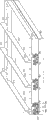
Fig. 5 illustrates the perspective illustration that has the longitudinal subdivision band and the substrate of horizontal dividing strip according to the present invention.As shown in the figure, on substrate 110, vertically form a plurality of longitudinal subdivision bands 52, and on substrate 110, laterally forming a plurality of horizontal dividing strips 55.On substrate 110, forming a plurality of pixels 62 between each longitudinal subdivision band 52 and between each horizontal dividing strip 55.That is, longitudinal subdivision band 52 is divided pixel 62 at vertical (that is, at column direction), and laterally dividing strip 55 is divided pixel 62 at horizontal (that is line direction).Utilize same color organic light emitting polymer 90 to apply each pixel 62 of arranging with row.Yet each pixel 62 of arranging with row has red (R), green (G) and blue (B) organic luminescence polymer 90 with alternating sequence.Therefore, longitudinal subdivision band 52 is divided R, G and B organic luminescence polymer 90, and prevents the horizontal interference of the organic luminescence polymer of neighbor.
As said with reference to figure 4, because surface tension, so at contact portion S, organic luminescence polymer 90 against vertically raises, and the planarization situation is poor.In order to prevent to occur this phenomenon in the present invention, longitudinal subdivision band 52 of the present invention has various sections, shown in Fig. 6 A to 6C.
Fig. 6 A to 6C is according to the cutaway view of longitudinal subdivision band of the present invention with horizontal dividing strip.For example, longitudinal subdivision band 52 shape that can have has: trapezoidal (shown in Fig. 6 A), semi-parabolic shape (shown in Fig. 6 B) or triangle (shown in Fig. 6 C).Also can adopt other shapes, so that the longitudinal subdivision band has sloped sidewall.According to various factors, comprise dividing strip material, etchant and etching speed and employed specific photoresist and developer, confirm the shape of sidewall.The inclined plane of longitudinal subdivision band 52 can with the angled φ of substrate.The value of angle φ can change between 0 to 90 degree.In addition, can also be what shape and the organic luminescence polymer that uses what type according to the dividing strip that is adopted, change the width W and the height H of longitudinal subdivision band 52.
Fig. 7 is the cutaway view of getting along the line VII-VII among Fig. 5.When longitudinal subdivision band 52 has inclined side as shown in Figure 7, utilize the organic luminescence polymer 90 of nozzle (Ref. No. 80 among Fig. 5) injection to glide along inclined side.Therefore, the contact portion S between longitudinal subdivision band 52 and organic luminescence polymer 90, the thickness of organic luminescence polymer 90 is not thick, thereby on whole base plate 110, realizes even planarization.
When horizontal dividing strip 55 shown in Figure 5 had the section shape shown in Fig. 6 A to 6C, organic luminescence polymer 90 that on horizontal dividing strip 55, forms and the organic luminescence polymer 90 that between longitudinal subdivision band 52, forms had same characteristic.Identical with longitudinal subdivision band 52, laterally dividing strip 55 can have for example trapezoidal (shown in Fig. 6 A), semi-parabolic shape (shown in Fig. 6 B) or triangle (shown in Fig. 6 C).Also can adopt other shapes, so that laterally dividing strip has sloped sidewall.Laterally the inclined side of dividing strip 55 can with the angled φ of fundamental substrate.The value of angle φ can change between 0 to 90 degree.In addition, can also be what shape and the organic luminescence polymer that uses what type according to the dividing strip that is adopted, change the width W and the height H of horizontal dividing strip.
In same processing step, form longitudinal subdivision band 52 and horizontal dividing strip 55 together.When forming longitudinal subdivision band 52, longitudinal subdivision band 52 is controlled so that it has the same height that is enough to prevent that the organic luminescence polymer 90 injected from overflowing with horizontal dividing strip 55.Yet formed horizontal dividing strip 55 can have various height.During photoresist is carried out mask process, utilize the diffraction exposure can realize these height change.Below will be with reference to figure 8A-8B and Fig. 9 A-9B explanation diffraction exposure process.
Fig. 8 A and 8B illustrate according to the present invention and utilize negative photoresist to form each processing step of dividing strip.
Shown in Fig. 8 A, on substrate 115, form organic layer 117.After this, on organic layer 117, form negative photoresist 120.After mask 140 being set to above the negative photoresist 120,, utilize ultraviolet ray (UV) irradiation photoresist 120 through mask 140.
In this exposure process, mask 140 comprises: the second portion that the first that the UV line passes through fully, UV line are stopped fully and some UV lines through and third part that some UV lines are stopped.First opens wide with the appropriate section irradiation UV line to negative photoresist 120 fully.The complete blocking UV line of the second portion of mask so that in developing process, is removed a part of negative photoresist 120 corresponding to this second portion.Third part comprises many slots 150 that are used for diffraction UV line, so that part UV line is through mask 140, and the appropriate section of irradiation negative photoresist 120 slightly.After passing through mask 140 irradiation UV, negative photoresist 120 is developed the figure into hope.Complete exposed portion corresponding to the negative photoresist 120 of first is kept intact.Corresponding to second portion fully not exposed portion be removed, so organic layer 117 is exposed.And corresponding to being removed slightly by the light exposure part of the negative photoresist 120 of third part, and do not had its original thickness, because this negative photoresist part is by the UV line exposing of diffraction.
Accomplish after the developing process, remaining photoresist and organic layer 117 are carried out etch processes.In etching during, also be etched corresponding to a part of organic layer 117 of second portion mask corresponding to a part of negative photoresist 120 of first's mask.In addition, remove remainder fully corresponding to the negative photoresist 120 of third part, and the top that part is removed organic layer 117.Therefore, form dividing strip 130 and 135 with different thickness at last, shown in Fig. 8 B.Corresponding to the thicker of the dividing strip 130 of the first of mask 140, so it can be used as longitudinal subdivision band 52 shown in Figure 5, or as highly high horizontal dividing strip 55.And corresponding to the thin thickness of the dividing strip 135 of the third part of mask 140, so it can be used as highly low horizontal dividing strip 55.
Fig. 9 A and 9B illustrate according to the present invention and utilize positive photoresist to form each processing step of dividing strip.
Shown in Fig. 9 A, on substrate 115, form organic layer 117.After this, on organic layer 117, form positive photoresist 122.After being provided with mask 160 above the positive photoresist 122, through mask 160, to positive photoresist 122 irradiation ultraviolet (UV) lines.
In this exposure process, mask 160 comprises: the second portion that the first that the UV line is stopped fully, UV line pass through fully and some UV lines through and third part that some UV lines are stopped.
The complete blocking UV line of the first of mask 160 so that in developing process, is removed a part of positive photoresist 122 corresponding to this first.Second portion opens wide with the appropriate section irradiation UV line to positive photoresist 122 fully.Third part comprises many slots 170 that are used for diffraction UV line, so that part UV line passes through mask 160, and the appropriate section of slight irradiation negative photoresist 122.After passing through mask 160 irradiation UV, positive photoresist 122 is developed the figure into hope.Complete unexposed portion corresponding to the positive photoresist 122 of the first of mask 160 is kept intact.Complete exposed portion corresponding to the photoresist 122 of the second portion of mask 160 is removed, so organic layer 117 is exposed.And corresponding to being removed slightly by the light exposure part of the positive photoresist 122 of third part, and do not had its original thickness, because this positive photoresist part is by the UV line exposing of diffraction.
Accomplish after the developing process, remaining photoresist and organic layer 117 are carried out etch processes.In etching during, also be etched corresponding to a part of organic layer 117 of the second portion of mask 160 corresponding to a part of positive photoresist 122 of first's mask.In addition, remove remainder fully, and part is removed the top corresponding to the organic layer 117 of third part corresponding to the positive photoresist 122 of third part.Therefore, identical with the negative photoresist technology shown in Fig. 8 A and the 8B, form dividing strip 130 and 135 with different thickness at last, shown in Fig. 9 B.Corresponding to the thicker of the dividing strip 130 of the first of mask 160, so it can be used as longitudinal subdivision band 52 shown in Figure 5, or as highly high horizontal dividing strip 55.And corresponding to the thin thickness of the dividing strip 135 of the third part of mask 160, so it can be used as highly low horizontal dividing strip 55.
As said,, can in same mask process, form longitudinal subdivision band 52 and horizontal dividing strip 55 together although longitudinal subdivision band 52 has different thickness with horizontal dividing strip 55 with reference to figure 8A-8B and 9A-9B.Because mask 140 or 160 has slot part 150 and 170 and utilize the diffraction of UV line, thus can make formed horizontal dividing strip 55 have different height, and can make formed longitudinal subdivision band 52 have homogeneous thickness.
Figure 10 is the cutaway view of getting along the line X-X among Fig. 5, and the process that on horizontal dividing strip, forms organic luminescence polymer is shown according to the present invention.
Horizontal dividing strip 55 with differing heights is set on substrate 110, then,, on substrate 110 and horizontal dividing strip 55, applies organic luminescence polymer 90 to utilize the mode of nozzle 80 injections.As said with reference to figure 6A-6C, laterally dividing strip 55 has sloped sidewall, and the organic luminescence polymer 90 that therefore applies maybe be along these sidewalls to lower slider.Therefore, can obtain the organic luminescence polymer 90 of even planarization.In addition, laterally dividing strip 55 light emitting polymer 90 that prevents to be injected at the edge of substrate 110 to dirty.
According to the height and the width of horizontal dividing strip 55, control the thickness of coated organic luminescence polymer 90.In addition, can also utilize the injection process of nozzle to control the thickness of coated organic luminescence polymer 90.The injection volume of the sweep speed of nozzle 80 and organic luminescence polymer 90 is confirmed the thickness of light emitting polymer 90.In order to control and the thickness of definite organic luminescence polymer 90,, gather experimental data through repeating experiment.Before forming horizontal dividing strip 55, on substrate 110, carry out nozzle scan, then, quantize (datumize) nozzle scan speed and injection volume, but also quantize the thickness of coated organic luminescence polymer.Data according to quantizing can design horizontal dividing strip 55, make it have optimum height and width.Through height and the width of controlling horizontal dividing strip, can form and have the organic luminescence polymer 90 of hoping thickness.If nozzle 80 is injected a small amount of organic luminescence polymer 90 on some horizontal dividing strips, then can design these dividing strips, make that it is highly high, width is wide.If nozzle 80 is injected a large amount of organic luminescence polymers 90 on some horizontal dividing strips, then can design these dividing strips, make it highly low, narrow width.
In addition, as stated, laterally dividing strip 55 can prevent that coated organic luminescence polymer 90 from flowing out to outside the substrate 110 downwards.In conventional art, in the end that is formed on the groove between each longitudinal subdivision band 52, organic luminescence polymer 90 is to dirty.Yet, in the present invention,,, therefore on whole base plate 110, realize planarization good, uniform thickness so coated organic luminescence polymer 90 is no longer lost because laterally dividing strip 55 stops to dirty.
In the present invention, can design the height of horizontal dividing strip, make its height less than the longitudinal subdivision band.Laterally the minimum altitude of dividing strip is equal to, or greater than the thickness of coated organic luminescence polymer.
Below will passive matrix and the active matrix type organic electroluminescent device that comprise above-mentioned longitudinal subdivision band and horizontal dividing strip be described with reference to figure 11-12 and 13-14.
Figure 11 is the perspective view according to passive matrix organic electroluminescence device of the present invention.
Shown in figure 11, form first electrode 202 on the substrate 200 of first, second that limits comprising and the 3rd pixel Rp, Gp and Bp.On first electrode 202, form each longitudinal subdivision band 204 with same height.Although not shown among Figure 11, also on first electrode 202, form horizontal dividing strip (Ref. No. 206 among Figure 12 A), yet laterally dividing strip have different height and width.Although longitudinal subdivision band 204 has same height, they can have different widths W.
On pixel Rp, Gp and Bp, be respectively arranged with machine light-emitting polymer layer 210,214 and 216.The organic luminescence polymer layer 210 that on pixel Rp, forms sends ruddiness, and the organic luminescence polymer layer 216 that on pixel Gp, forms sends green glow, and the organic luminescence polymer layer 214 that on pixel B p, forms sends blue light.On each organic luminescence polymer layer 210,216 and 214, form second electrode 220 respectively.Second electrode 220 is isolated with second electrode electricity of neighbor, so each pixel Rp, Gp and Bp comprise one second electrode 220 respectively.First electrode 202 injects the hole in organic light-emitting polymer layer 210,216 and 214, therefore usually it is called anode.Second electrode 220 injects electronics in organic light-emitting polymer layer 210,216 and 214, therefore usually it is called negative electrode.
Still with reference to Figure 11, on the upper surface of organic luminescence polymer layer 210,216 and 214 and lower surface, form hole moving layer 203 and electron transfer layer 218 respectively.Because have hole moving layer 203 and electron transfer layer 218, so charge carrier (hole and electronics) does not directly inject organic light-emitting polymer layer 210,216 and 214.Because charge carrier arrives organic luminescence polymer layer 210,216 and 214 (promptly through migrating layer 203 and 218 from electrode 202 and 220; Two steps injected); So can improve quantum efficiency (number of photons (photo-outper injected-charge) that each electric charge of injection is emitted), and can reduce driving voltage.
When on organic luminescence polymer layer 210,216 and 214, forming second electrode 220, the control direction of deposition is to form second electrode 220 respectively on each pixel Rp, Gp and Bp.A kind of mode of control direction of deposition is that substrate 200 is tilted.Substrate tilts can prevent second electrode 220 overlapping longitudinal subdivision band 204 in deposition process, so that on each pixel Rp, Gp and Bp, form second electrode 220 respectively.The another kind of mode of control direction of deposition is the target location of control second electrode 220.Through moving the target location of second electrodeposition, also can on each pixel Rp, Gp and Bp, form second electrode 220 respectively.That is, the control direction of deposition can make second electrode 220 only be formed on organic luminescence polymer layer 210,216 and 214 directly over and also be positioned on the top and sloped sidewall of longitudinal subdivision band 204.
Through on substrate, utilizing nozzle to apply as stated, can form passive matrix organic electroluminescence device shown in Figure 11 with longitudinal subdivision band of the present invention and horizontal dividing strip.Figure 12 A to 12C illustrates each processing step that forms passive matrix organic electroluminescence device shown in Figure 11.
With reference to figure 12A, substrate 200 comprises first, second and the 3rd pixel Rp, Gp and Bp.Define above that on the substrate 220 of first, second and the 3rd pixel Rp, Gp and Bp and form first electrode 202.As stated, first electrode 202 is the anodes with high work function (work function).For example, first electrode 202 can be formed by tin indium oxide (ITO).Then, on first electrode 202, form longitudinal subdivision band 204 and horizontal dividing strip 206 together.Longitudinal subdivision band 204 is with laterally dividing strip 206 is by polymer substance, and for example polyimides forms.In addition, utilize one of technology of describing with reference to figure 8A-8B and 9A-9B to form longitudinal subdivision band 204 and horizontal dividing strip 206.Because utilize the mask with many slots to carry out the diffraction exposure, so longitudinal subdivision band 204 has same height, and has inclined side, and laterally dividing strip 206 has different height and width, and has inclined side.After this, on first electrode 202, form hole moving layer 203.
Then, in Figure 12 B, the method for utilizing nozzle to apply forms organic light-emitting polymer layer 210,216 and 214 respectively on first, second and the 3rd pixel Rp, Gp and Bp.Organic luminescence polymer layer 210,216 and 214 sends ruddiness, green glow and blue light respectively.Forming organic light-emitting polymer layer 210,216 and respectively at 214 o'clock, laterally applying organic luminescence polymer on the dividing strip 206, shown in figure 10.Yet, because laterally dividing strip 206 has sloped sidewall, so organic luminescence polymer, therefore makes first, second and the 3rd pixel Rp, Gp and the even planarization of Bp to lower slider.
In Figure 12 C, polymer substance is coated on organic luminescence polymer layer 210,216 and 214 to form electron transfer layer 218.Can be only on first, second and the 3rd pixel Rp, Gp and Bp, perhaps at first, second and the 3rd pixel Rp, Gp and Bp and laterally form electron transfer layer 218 on the dividing strip 206.After this, deposit has the conductor material of low work function on whole base plate 200, for example aluminium (Al), magnesium (Mg) or calcium (Ca), thus form second electrode 220 (that is negative electrode).As stated, when forming second electrode 220, the control direction of deposition is to form second electrode 220 respectively on first, second and the 3rd pixel Rp, Gp and Bp.Shown in Figure 12 C, longitudinal subdivision band 206 plays dividing plate, and it is separately positioned on first, second and the 3rd pixel Rp, Gp and the Bp each layer elements.
Figure 13 is the perspective view according to active matrix type organic electroluminescent device of the present invention.
Shown in figure 13, have above that on the substrate 300 of first, second and the 3rd pixel Rp, Gp and Bp and form thin-film transistor (TFT) T.Each TFT T is separately positioned on first, second and the 3rd pixel Rp, Gp and the Bp, and each TFT T has grid 304, active layer 302, source electrode 306 and drains 308.When covering TFT T, passivation layer 310 is set on whole base plate 300.On the passivation layer 310 at each on first, second and the 3rd pixel Rp, Gp and the Bp first electrode 312 is set.First electrode 312 contacts the drain electrode 308 of TFT T through the drain contact hole that runs through passivation layer 310.In addition, order is provided with hole moving layer 316, organic luminescence polymer layer 322,326 or 328 and electron transfer layer 330 on first electrode of each pixel Rp, Gp and Bp.Second electrode 332 is set in place on the electron transfer layer on the whole base plate 300 330.
Still, a plurality of longitudinal subdivision bands 314 are set on passivation layer 310 with reference to Figure 13.Although not shown in Figure 13, in Figure 14 B, illustrated, laterally dividing strip 315 also is arranged on the passivation layer 310.Along the boundary setting longitudinal subdivision band 314 of first, second and the 3rd pixel Rp, Gp and Bp and horizontal dividing strip 315, so that they are divided each layer elements (first electrode 312, hole moving layer 316, organic luminescence polymer layer 322,326 and 328, electron transfer layer 330) and be isolated in first, second and the 3rd pixel Rp, Gp and the Bp.That is, longitudinal subdivision band 314 prevents further that with horizontal dividing strip 315 organic material is diffused into neighbor.In addition, as stated, longitudinal subdivision band 314 can make coated organic material have homogeneous thickness and level with horizontal dividing strip 315.
Figure 14 A to 14D illustrates each processing step that forms active matrix type organic electroluminescent device shown in Figure 13.
With reference to figure 14A, on transparent plastic or glass substrate 300, limit first, second and the 3rd pixel Rp, Gp and Bp.Pixel Rp is used to glow, and pixel Gp is used for green light, and pixel B p is used for blue light-emitting.In each pixel Rp, Gp or Bp, on substrate 300, form thin-film transistor (TFT) T.As stated, TFT T comprises active layer 302, grid 304, source electrode 306 and drains 308.After this, in order to cover TFT T, on substrate 300, form organic material, thereby form passivation layer 310 such as benzocyclobutene (BCB) or acrylic resin.Then, composition passivation layer 310 exposes the drain contact hole of the drain electrode 308 of TFT T with formation.
In Figure 14 B, form first electrode 312 independently among first, second and the 3rd pixel Rp, Gp and the Bp at each.First electrode 312 is the transparency conductive electrodes with high work function, for example tin indium oxide (ITO).After this, the border along first, second and the 3rd pixel Rp, Gp and Bp is vertically forming longitudinal subdivision band 314.As said with reference to figure 5-9, longitudinal subdivision band 314 has same height and sloped sidewall.When forming longitudinal subdivision band 314, also form horizontal dividing strip 315.Owing to utilize diffraction of light to form horizontal dividing strip 315, as said, so laterally dividing strip 315 can have different height and width with reference to figure 8A-8B and 9A-9B.On the border of pixel up and down, at the horizontal dividing strip 315 of horizontally set, and laterally dividing strip 315 also has sloped sidewall.Because longitudinal subdivision band 314 has many slots and utilizes diffraction of light with the mask of horizontal dividing strip 315, so can obtain the dividing strip of differing heights and width according to the present invention.After forming longitudinal subdivision band 314 and horizontal dividing strip 315, on whole base plate, apply organic material to form hole moving layer 316.Because longitudinal subdivision band 314 has sloped sidewall with horizontal dividing strip 315, and coated organic material can slide along sloped sidewall, so can in first, second and the 3rd pixel Rp, Gp and Bp, form the hole moving layer 316 of organic material.
Now, in Figure 14 C, adopt the nozzle painting method of describing with reference to Figure 10, on hole moving layer 316, form organic light-emitting polymer layer 322,326 and 328.Organic luminescence polymer layer 322,326 and 328 glows respectively, green glow and blue light.Because longitudinal subdivision band 314 and horizontal dividing strip 315 have the height and the width of sloped sidewall and hope, the planarization and have uniform thickness so organic luminescence polymer layer 322,326 and 328 becomes.After forming organic light-emitting polymer layer 322,326 and 328, on organic luminescence polymer layer 322,326 and 328, apply organic material to form electron transfer layer 330.
Then, in Figure 14 D, deposit has the electric conducting material of low work function on whole base plate 300, for example aluminium (Al), magnesium (Mg) or calcium (Ca), thus form second electrode 332 (that is negative electrode).
According to the present invention of above description, have inclined side and have differing heights and the longitudinal subdivision band of width during in formation with horizontal dividing strip, utilize negative photoresist or positive photoresist, carry out the diffraction exposure.In addition, on substrate, utilize nozzle to apply organic light-emitting polymer layer with longitudinal subdivision band and horizontal dividing strip.Therefore, the organic luminescence polymer layer that on each pixel, forms show good planarization and also thickness even.The organic electroluminescence device that comprises this organic luminescence polymer layer can have good display characteristic.In addition,, need not be used to form the additional process of longitudinal subdivision band or horizontal dividing strip, therefore reduce production cost owing to utilize same mask and diffraction exposure to form horizontal dividing strip and longitudinal subdivision band together.
Should be understood that; Although above process to employing nozzle coating formation electroluminescent organic material is illustrated; But can estimate, can utilize other painting methods that electroluminescent organic material is deposited on the pixel region of substrate, for example can use " ink-jet " painting method.As a kind of typical ink-jet painting method, comprise that the ink gun of the jet orifice of storage print cartridge and a plurality of alignings passes through on substrate, the ink droplet from a plurality of jet orifice injection electroluminescent organic materials is expelled to ink droplet in the pixel region of substrate.
Ink gun can have a plurality of chambers that link to each other with each jet orifice respectively; Therefore for example through the piezoelectric crystal that links to each other with chamber is applied electric current; And chamber is exerted pressure or made its when vibration, the ink droplet of electroluminescent organic material just is expelled to pixel region from jet orifice.Through changing size, the number of ink droplets of each pixel, the sweep speed of ink gun or their combination of ink droplet, can control the quantity that is expelled to the electroluminescent organic material in the pixel region.
Ink gun preferably along the pixel on the substrate vertically, move with the linear reciprocation mode.As a kind of selection, during the deposit electroluminescent organic material, can make ink gun keep static, and moving substrate, perhaps during the deposit electroluminescent organic material, ink gun and substrate can move relative to one another.In order to utilize electroluminescent organic material to fill each pixel on the whole base plate, ink gun is passed through repeatedly.
Can utilize polymer organic electroluminescence material to carry out ink-jet, also can utilize the unimolecule electroluminescent organic material to carry out ink-jet.
Although the embodiment of the invention shown in the reference specifies and describes the present invention; But; Those of skill in the art in the present technique field understand, in essential scope of the present invention, can aspect form and details, carry out above and other modifications to the present invention.
Claims (21)
1. organic electroluminescence device, this organic electroluminescence device comprises:
Transparency carrier has first pixel, second pixel and the 3rd pixel that limit at least above that;
The first longitudinal subdivision band is between said first pixel and said second pixel;
The second longitudinal subdivision band is between said second pixel and said the 3rd pixel;
The first horizontal dividing strip extends between said first longitudinal subdivision band and the said second longitudinal subdivision band;
A plurality of first electrodes are formed on the said transparency carrier, the said first horizontal dividing strip longitudinally and the said first longitudinal subdivision band and the second longitudinal subdivision band along laterally dividing said a plurality of first electrodes;
The organic luminescence polymer layer is on said a plurality of first electrodes, between said first longitudinal subdivision band and the said second longitudinal subdivision band; And
Second electrode, on said organic luminescence polymer layer and cover the whole surface of said transparency carrier,
Each of the wherein said first longitudinal subdivision band and the second longitudinal subdivision band has an independent layer,
The height of the wherein said first horizontal dividing strip is less than the height of the said first longitudinal subdivision band,
Wherein, the sidewall of said first longitudinal subdivision band and the said second longitudinal subdivision band is that clinoplain and whole clinoplain are outward-dipping, and
Wherein utilize mask to form the said first longitudinal subdivision band and the second longitudinal subdivision band and the said first horizontal dividing strip simultaneously, stop portions and part that this mask has the transmissive part that sees through ultraviolet radiation fully, complete shielding of ultraviolet radiation see through and the mid portion of part shielding of ultraviolet radiation.
2. organic electroluminescence device according to claim 1, the sidewall of the wherein said first horizontal dividing strip is outward-dipping.
3. organic electroluminescence device according to claim 2, the said inclination of wherein said sidewall is linear.
4. organic electroluminescence device according to claim 2, the said inclination of wherein said sidewall is non-linear, makes that said sidewall is an arch.
5. organic electroluminescence device according to claim 2, wherein said sidewall is tapered towards the point on the said horizontal dividing strip top.
6. organic electroluminescence device according to claim 2, the top of wherein said horizontal dividing strip is smooth.
7. organic electroluminescence device according to claim 2, the section shape of wherein said horizontal dividing strip are one of trapezoidal cross-section, triangular cross-section and semi-parabolic shape section.
8. organic electroluminescence device according to claim 1; This organic electroluminescence device further is included in the second horizontal dividing strip that extends between said first longitudinal subdivision band and the said second longitudinal subdivision band, and wherein said second pixel is surrounded by the said first longitudinal subdivision band, the said second longitudinal subdivision band, the said first horizontal dividing strip and the said second horizontal dividing strip.
9. organic electroluminescence device according to claim 1, wherein
Each said first pixel, second pixel and the 3rd pixel are associated with corresponding first electrode respectively.
10. organic electroluminescence device according to claim 9, this organic electroluminescence device further comprises:
A plurality of thin-film transistors are formed on the said substrate, and each said first pixel, second pixel and the 3rd pixel are associated with a corresponding thin-film transistor respectively.
11. organic electroluminescence device according to claim 1; Wherein each said first pixel, second pixel and the 3rd pixel comprise said organic luminescence polymer layer respectively; And in said first pixel, second pixel and the 3rd pixel, said organic luminescence polymer layer sends ruddiness, green glow and blue light respectively.
12. a method of making organic electroluminescence device, this method may further comprise the steps:
Transparency carrier is provided, has first pixel, second pixel and the 3rd pixel on this transparency carrier;
On said transparency carrier, organic layer is provided;
Photoresist is provided on organic layer;
Mask is set on photoresist, and stop portions and part that this mask has the transmissive part that sees through ultraviolet radiation fully, complete shielding of ultraviolet radiation see through and the mid portion of part shielding of ultraviolet radiation;
Pass through mask; Utilize the ultraviolet irradiation photoresist; To form simultaneously at the first longitudinal subdivision band between said first pixel and said second pixel, at the second longitudinal subdivision band between said second pixel and said the 3rd pixel and the first horizontal dividing strip that between said first longitudinal subdivision band and the said second longitudinal subdivision band, extends; The sidewall of wherein said first longitudinal subdivision band and the said second longitudinal subdivision band is that clinoplain and whole clinoplain are outward-dipping; The height of the said first horizontal dividing strip is less than the height of the said first longitudinal subdivision band, and each of the wherein said first longitudinal subdivision band and the second longitudinal subdivision band has an independent layer;
On said transparency carrier, form a plurality of first electrodes, the said first horizontal dividing strip longitudinally and the said first longitudinal subdivision band and the second longitudinal subdivision band along horizontal said a plurality of first electrodes of division;
On said a plurality of first electrodes, between said first longitudinal subdivision band and the said second longitudinal subdivision band, organic light-emitting polymer layer is provided; And
On the said organic luminescence polymer layer on the whole said transparency carrier, form second electrode.
13. the method for manufacturing organic electroluminescence device according to claim 12 wherein forms horizontal dividing strip in the position corresponding to the mid portion of mask.
14. the method for manufacturing organic electroluminescence device according to claim 12 wherein provides the step of organic light-emitting polymer layer to comprise and utilizes nozzle to apply the step of organic light-emitting polymer layer.
15. the injection volume that the method for manufacturing organic electroluminescence device according to claim 14, this method further comprise the sweep speed of controlling nozzle and organic luminescence polymer is with the step of the deposit amount of controlling the organic luminescence polymer between each longitudinal subdivision band.
16. further being included in, the method for manufacturing organic electroluminescence device according to claim 14, this method apply the step that during organic light-emitting polymer layer substrate is tilted.
17. the method for manufacturing organic electroluminescence device according to claim 12, wherein
Each said first pixel, second pixel and the 3rd pixel are associated with corresponding one first electrode respectively.
18. the method for manufacturing organic electroluminescence device according to claim 17; This method further is included in the step that forms a plurality of thin-film transistors on the said substrate, and each said first pixel, second pixel and the 3rd pixel are associated with a corresponding thin-film transistor respectively.
19. the method for manufacturing organic electroluminescence device according to claim 12; Wherein on said substrate, provide the step of organic light-emitting polymer layer to comprise the step that said first pixel, second pixel and the 3rd pixel is provided organic luminescence polymer respectively; Wherein in said first pixel, second pixel and the 3rd pixel, this organic luminescence polymer sends ruddiness, green glow and blue light respectively.
20. the method for manufacturing organic electroluminescence device according to claim 12 wherein provides the step of organic light-emitting polymer layer to comprise and utilizes the ink-jet painting method to apply the step of organic light-emitting polymer layer.
21. the method for manufacturing organic electroluminescence device according to claim 20, wherein coating step is included in and carries out ink-jet on the substrate, and between the longitudinal subdivision band, is deposited to the ink droplet of organic luminescence polymer in each pixel of substrate.
Applications Claiming Priority (2)
| Application Number | Priority Date | Filing Date | Title |
|---|---|---|---|
| KR68570/2002 | 2002-11-06 | ||
| KR10-2002-0068570A KR100508002B1 (en) | 2002-09-03 | 2002-11-06 | fabrication method of an organic electro-luminescence device using nozzle coating |
Related Parent Applications (1)
| Application Number | Title | Priority Date | Filing Date |
|---|---|---|---|
| CNA2003101038135A Division CN1499907A (en) | 2002-11-06 | 2003-11-06 | Organic electroluminescent device with oblique banks and coating fabrication technique |
Publications (2)
| Publication Number | Publication Date |
|---|---|
| CN102324432A true CN102324432A (en) | 2012-01-18 |
| CN102324432B CN102324432B (en) | 2014-01-29 |
Family
ID=32588764
Family Applications (2)
| Application Number | Title | Priority Date | Filing Date |
|---|---|---|---|
| CN201110156105.2A Expired - Lifetime CN102324432B (en) | 2002-11-06 | 2003-11-06 | Organic electroluminescent device with inclined separation zone and coating manufacturing technology |
| CNA2003101038135A Pending CN1499907A (en) | 2002-11-06 | 2003-11-06 | Organic electroluminescent device with oblique banks and coating fabrication technique |
Family Applications After (1)
| Application Number | Title | Priority Date | Filing Date |
|---|---|---|---|
| CNA2003101038135A Pending CN1499907A (en) | 2002-11-06 | 2003-11-06 | Organic electroluminescent device with oblique banks and coating fabrication technique |
Country Status (3)
| Country | Link |
|---|---|
| US (1) | US7365367B2 (en) |
| KR (1) | KR100508002B1 (en) |
| CN (2) | CN102324432B (en) |
Cited By (8)
| Publication number | Priority date | Publication date | Assignee | Title |
|---|---|---|---|---|
| CN103208508A (en) * | 2013-04-27 | 2013-07-17 | 上海大学 | Organic electroluminescent display screen, coating device special for organic electroluminescent display screen and manufacturing method for organic electroluminescent display screen |
| CN105336881A (en) * | 2015-11-04 | 2016-02-17 | Tcl集团股份有限公司 | Printing type high-resolution display device and manufacturing method thereof |
| CN105428553A (en) * | 2015-11-11 | 2016-03-23 | Tcl集团股份有限公司 | Printing type display device and manufacturing method thereof |
| CN111312760A (en) * | 2018-12-11 | 2020-06-19 | 乐金显示有限公司 | Organic light emitting display device and method of manufacturing the same |
| CN111312758A (en) * | 2018-12-11 | 2020-06-19 | 乐金显示有限公司 | Organic light-emitting display device and method of manufacturing the same |
| JP2020537281A (en) * | 2017-10-13 | 2020-12-17 | 京東方科技集團股▲ふん▼有限公司Boe Technology Group Co.,Ltd. | Array board, display panel, display device and its manufacturing method |
| CN115036355A (en) * | 2022-07-27 | 2022-09-09 | 合肥京东方卓印科技有限公司 | Display panel, manufacturing method and display device |
| WO2023225953A1 (en) * | 2022-05-26 | 2023-11-30 | 京东方科技集团股份有限公司 | Display substrate and display device |
Families Citing this family (60)
| Publication number | Priority date | Publication date | Assignee | Title |
|---|---|---|---|---|
| AUPQ790100A0 (en) * | 2000-06-01 | 2000-06-22 | Telstra R & D Management Pty Ltd | A validation system |
| EP1665894A4 (en) * | 2003-09-16 | 2009-12-16 | Daewoo Electronics Service Co | Organic electroluminescent display and method of making the same |
| KR100705312B1 (en) | 2004-03-22 | 2007-04-10 | 엘지전자 주식회사 | Organic electroluminescent device and manufacturing method thereof |
| US20050282308A1 (en) * | 2004-06-22 | 2005-12-22 | Albrecht Uhlig | Organic electroluminescent display device and method of producing the same |
| JP2006038987A (en) * | 2004-07-23 | 2006-02-09 | Seiko Epson Corp | Display device, display device manufacturing method, and electronic apparatus |
| US20060228466A1 (en) * | 2004-12-30 | 2006-10-12 | Gang Yu | Solution dispense and patterning process and apparatus |
| US7584701B2 (en) * | 2004-12-30 | 2009-09-08 | E.I. Du Pont De Nemours And Company | Processes for printing layers for electronic devices and printing apparatuses for performing the processes |
| US20060146079A1 (en) * | 2004-12-30 | 2006-07-06 | Macpherson Charles D | Process and apparatus for forming an electronic device |
| US7469638B2 (en) * | 2004-12-30 | 2008-12-30 | E.I. Du Pont De Nemours And Company | Electronic devices and processes for forming the same |
| US20060145598A1 (en) * | 2004-12-30 | 2006-07-06 | Macpherson Charles D | Electronic devices and process for forming the same |
| KR101112534B1 (en) | 2005-03-04 | 2012-03-13 | 삼성전자주식회사 | Organic light emitting display and method for manufacturing the same |
| KR20060114251A (en) * | 2005-04-29 | 2006-11-06 | 삼성전자주식회사 | Manufacturing method of liquid crystal display and alignment film forming apparatus used therein |
| US7645177B2 (en) | 2005-05-07 | 2010-01-12 | Hewlett-Packard Development Company, L.P. | Electroluminescent panel with inkjet-printed electrode regions |
| KR101219045B1 (en) | 2005-06-29 | 2013-01-07 | 삼성디스플레이 주식회사 | Display device and manufacturing method of the same |
| JP2007188862A (en) * | 2005-12-13 | 2007-07-26 | Canon Inc | Organic EL light emitting device and method for manufacturing the same |
| JP2007234232A (en) * | 2006-02-27 | 2007-09-13 | Hitachi Displays Ltd | Image display device |
| KR100738224B1 (en) * | 2006-03-31 | 2007-07-12 | 엘지전자 주식회사 | Electroluminescent element |
| US7633218B2 (en) * | 2006-09-29 | 2009-12-15 | Eastman Kodak Company | OLED device having improved lifetime and resolution |
| EP2151867B1 (en) * | 2007-05-30 | 2016-08-03 | Joled Inc. | Organic el display panel |
| JP4280301B2 (en) | 2007-05-31 | 2009-06-17 | パナソニック株式会社 | Organic EL device and method for manufacturing the same |
| KR101367136B1 (en) * | 2007-07-27 | 2014-02-25 | 삼성디스플레이 주식회사 | Organic light emitting device and manufacturing method thereof |
| JP2009043499A (en) * | 2007-08-08 | 2009-02-26 | Canon Inc | Organic EL device substrate and method for producing the same |
| JP2009070859A (en) * | 2007-09-10 | 2009-04-02 | Casio Comput Co Ltd | Organic electroluminescence display device and manufacturing method thereof |
| JP5448030B2 (en) * | 2008-11-19 | 2014-03-19 | 新日鐵住金株式会社 | Ultrasonic flaw detection method and apparatus |
| KR101613865B1 (en) * | 2009-03-26 | 2016-04-20 | 가부시키가이샤 한도오따이 에네루기 켄큐쇼 | Light-emitting device and method for manufacturing the same |
| JP2011108578A (en) * | 2009-11-20 | 2011-06-02 | Toppan Printing Co Ltd | Organic el light emitting element and method of manufacturing the same |
| KR101643009B1 (en) * | 2009-12-22 | 2016-07-27 | 가부시키가이샤 제이올레드 | Display device and method for manufacturing the same |
| WO2012017498A1 (en) * | 2010-08-06 | 2012-02-09 | パナソニック株式会社 | Organic el display panel, and method for producing same |
| KR20130044118A (en) * | 2010-08-06 | 2013-05-02 | 파나소닉 주식회사 | Organic el display panel, display device, and method of manufacturing organic el display panel |
| KR101881083B1 (en) | 2011-11-09 | 2018-07-24 | 삼성디스플레이 주식회사 | Organic light emitting display device |
| WO2013093974A1 (en) * | 2011-12-22 | 2013-06-27 | パナソニック株式会社 | Organic el display panel |
| CN102593115A (en) * | 2012-03-15 | 2012-07-18 | 深圳市丽晶光电科技股份有限公司 | LED surface-mounted device and manufacturing method thereof |
| US8981391B2 (en) * | 2012-06-22 | 2015-03-17 | Industrial Technology Research Institute | Display panel with high transparency |
| KR101632298B1 (en) * | 2012-07-16 | 2016-06-22 | 삼성디스플레이 주식회사 | Flat panel display device and manufacturing method thereof |
| KR102090112B1 (en) * | 2013-05-31 | 2020-03-17 | 엘지디스플레이 주식회사 | Method of manufacturing an organic light emitting device using the spin coating |
| JP6248269B2 (en) * | 2014-02-06 | 2017-12-20 | 株式会社Joled | Display device |
| CN103887261B (en) * | 2014-03-03 | 2016-08-31 | 京东方科技集团股份有限公司 | A kind of flexible display and preparation method thereof |
| US10910350B2 (en) * | 2014-05-24 | 2021-02-02 | Hiphoton Co., Ltd. | Structure of a semiconductor array |
| CN104241329A (en) * | 2014-08-22 | 2014-12-24 | 京东方科技集团股份有限公司 | Display panel provided with pixel defining layer and manufacturing method of pixel defining layer |
| JP2016091942A (en) * | 2014-11-10 | 2016-05-23 | 株式会社Joled | Display device and manufacturing method thereof |
| CN104409366A (en) * | 2014-11-19 | 2015-03-11 | 三星半导体(中国)研究开发有限公司 | Chip encapsulating method and encapsulating substrate |
| CN104465671B (en) * | 2014-12-26 | 2016-08-31 | 京东方科技集团股份有限公司 | A kind of display base plate and preparation method thereof, display device |
| CN104867963A (en) * | 2015-05-08 | 2015-08-26 | 京东方科技集团股份有限公司 | Organic light emitting display substrate, production method thereof, organic light emitting display device |
| JP6741431B2 (en) * | 2016-01-25 | 2020-08-19 | 株式会社Joled | Display panel and manufacturing method thereof |
| JP6815090B2 (en) * | 2016-03-31 | 2021-01-20 | 株式会社Joled | Display panel and its manufacturing method |
| KR20180132935A (en) * | 2016-05-30 | 2018-12-12 | 가부시키가이샤 제이올레드 | Display and electronic devices |
| US10448519B2 (en) | 2016-07-01 | 2019-10-15 | Hzo, Inc. | Method of masking and de-masking |
| WO2018033510A2 (en) | 2016-08-17 | 2018-02-22 | Merck Patent Gmbh | Electronic device with bank structures |
| CN106784352B (en) * | 2016-12-28 | 2019-03-29 | 固安翌光科技有限公司 | Organic luminescent device and its manufacturing method |
| JP2019046599A (en) * | 2017-08-31 | 2019-03-22 | 株式会社ジャパンディスプレイ | Display device |
| WO2019127253A1 (en) * | 2017-12-28 | 2019-07-04 | 深圳市柔宇科技有限公司 | Display device and electronic device |
| KR102689217B1 (en) * | 2018-12-14 | 2024-07-26 | 엘지디스플레이 주식회사 | Electroluminescent Device |
| CN113632590B (en) * | 2019-03-28 | 2024-11-22 | 夏普株式会社 | Display components |
| JP7344004B2 (en) * | 2019-04-26 | 2023-09-13 | Tianma Japan株式会社 | OLED display device and method for manufacturing the OLED display device |
| CN110311057A (en) * | 2019-07-29 | 2019-10-08 | 云谷(固安)科技有限公司 | Display panel and preparation method thereof and display device |
| CN111293152B (en) * | 2020-02-20 | 2022-11-04 | 京东方科技集团股份有限公司 | Display substrate and preparation method thereof, and electroluminescence display device |
| US20210351246A1 (en) * | 2020-05-06 | 2021-11-11 | Wuhan China Star Optoelectronics Semiconductor Display Technology Co., Ltd. | Pixel layout structure of oled, oled display panel, and manufacturing method thereof |
| CN111584605B (en) | 2020-05-29 | 2023-04-07 | 京东方科技集团股份有限公司 | Array substrate, preparation method, display panel and display device |
| TWI757097B (en) | 2021-02-17 | 2022-03-01 | 友達光電股份有限公司 | Display panel |
| CN113053967A (en) | 2021-03-09 | 2021-06-29 | 深圳市华星光电半导体显示技术有限公司 | Display panel, preparation method thereof and display device |
Citations (1)
| Publication number | Priority date | Publication date | Assignee | Title |
|---|---|---|---|---|
| CN1353866A (en) * | 1999-11-29 | 2002-06-12 | 皇家菲利浦电子有限公司 | Organic electroluminescent device and method of manufacturing thereof |
Family Cites Families (11)
| Publication number | Priority date | Publication date | Assignee | Title |
|---|---|---|---|---|
| JP3885303B2 (en) * | 1997-08-29 | 2007-02-21 | セイコーエプソン株式会社 | Manufacturing method of light emitting substrate |
| KR100669667B1 (en) * | 1998-05-29 | 2007-05-14 | 삼성에스디아이 주식회사 | Manufacturing method of polymer organic electroluminescent device |
| KR100269390B1 (en) * | 1998-07-28 | 2000-10-16 | 구자홍 | Electroluminescence display panel and method for producing thereof |
| KR100335102B1 (en) * | 1999-08-09 | 2002-05-04 | 구자홍 | Structure of Plasma Display Panel and Method for Driving the Plasma Display Panel |
| TW484238B (en) * | 2000-03-27 | 2002-04-21 | Semiconductor Energy Lab | Light emitting device and a method of manufacturing the same |
| JP2001279134A (en) * | 2000-03-31 | 2001-10-10 | Seiko Epson Corp | Discharge composition and method for producing functional film |
| US6900470B2 (en) * | 2001-04-20 | 2005-05-31 | Kabushiki Kaisha Toshiba | Display device and method of manufacturing the same |
| US20030166311A1 (en) * | 2001-09-12 | 2003-09-04 | Seiko Epson Corporation | Method for patterning, method for forming film, patterning apparatus, film formation apparatus, electro-optic apparatus and method for manufacturing the same, electronic equipment, and electronic apparatus and method for manufacturing the same |
| WO2003026360A1 (en) * | 2001-09-15 | 2003-03-27 | Cld, Inc. | Organic electroluminescence display and fabricating mehtod thereof |
| US20030053044A1 (en) * | 2001-09-18 | 2003-03-20 | Xerox Corporation | Color balance control in organic light emitting diode displays |
| US7488986B2 (en) * | 2001-10-26 | 2009-02-10 | Semiconductor Energy Laboratory Co., Ltd. | Light emitting device |
-
2002
- 2002-11-06 KR KR10-2002-0068570A patent/KR100508002B1/en not_active Expired - Lifetime
-
2003
- 2003-09-02 US US10/651,955 patent/US7365367B2/en not_active Expired - Lifetime
- 2003-11-06 CN CN201110156105.2A patent/CN102324432B/en not_active Expired - Lifetime
- 2003-11-06 CN CNA2003101038135A patent/CN1499907A/en active Pending
Patent Citations (1)
| Publication number | Priority date | Publication date | Assignee | Title |
|---|---|---|---|---|
| CN1353866A (en) * | 1999-11-29 | 2002-06-12 | 皇家菲利浦电子有限公司 | Organic electroluminescent device and method of manufacturing thereof |
Cited By (15)
| Publication number | Priority date | Publication date | Assignee | Title |
|---|---|---|---|---|
| CN103208508A (en) * | 2013-04-27 | 2013-07-17 | 上海大学 | Organic electroluminescent display screen, coating device special for organic electroluminescent display screen and manufacturing method for organic electroluminescent display screen |
| CN105336881A (en) * | 2015-11-04 | 2016-02-17 | Tcl集团股份有限公司 | Printing type high-resolution display device and manufacturing method thereof |
| CN105336881B (en) * | 2015-11-04 | 2018-05-08 | Tcl集团股份有限公司 | A kind of printed form high resolution display part and preparation method thereof |
| CN105428553A (en) * | 2015-11-11 | 2016-03-23 | Tcl集团股份有限公司 | Printing type display device and manufacturing method thereof |
| CN105428553B (en) * | 2015-11-11 | 2018-09-18 | 广东聚华印刷显示技术有限公司 | A kind of printed form display device and preparation method thereof |
| US11424303B2 (en) | 2017-10-13 | 2022-08-23 | Boe Technology Group Co., Ltd. | Array substrate, display panel, and display apparatus having a pixel defining layer with thickness thinning regions |
| US12048202B2 (en) | 2017-10-13 | 2024-07-23 | Boe Technology Group Co., Ltd. | Array substrate including pixel defining layer with spacer parts |
| JP2020537281A (en) * | 2017-10-13 | 2020-12-17 | 京東方科技集團股▲ふん▼有限公司Boe Technology Group Co.,Ltd. | Array board, display panel, display device and its manufacturing method |
| CN111312758A (en) * | 2018-12-11 | 2020-06-19 | 乐金显示有限公司 | Organic light-emitting display device and method of manufacturing the same |
| CN111312760B (en) * | 2018-12-11 | 2023-09-26 | 乐金显示有限公司 | Organic light-emitting display device and manufacturing method thereof |
| CN111312758B (en) * | 2018-12-11 | 2023-12-19 | 乐金显示有限公司 | Organic light-emitting display device and manufacturing method thereof |
| CN111312760A (en) * | 2018-12-11 | 2020-06-19 | 乐金显示有限公司 | Organic light emitting display device and method of manufacturing the same |
| WO2023225953A1 (en) * | 2022-05-26 | 2023-11-30 | 京东方科技集团股份有限公司 | Display substrate and display device |
| CN115036355A (en) * | 2022-07-27 | 2022-09-09 | 合肥京东方卓印科技有限公司 | Display panel, manufacturing method and display device |
| WO2024022056A1 (en) * | 2022-07-27 | 2024-02-01 | 京东方科技集团股份有限公司 | Display panel, fabrication method, and display device |
Also Published As
| Publication number | Publication date |
|---|---|
| CN1499907A (en) | 2004-05-26 |
| KR20040020783A (en) | 2004-03-09 |
| US20040119066A1 (en) | 2004-06-24 |
| US7365367B2 (en) | 2008-04-29 |
| CN102324432B (en) | 2014-01-29 |
| KR100508002B1 (en) | 2005-08-17 |
Similar Documents
| Publication | Publication Date | Title |
|---|---|---|
| CN102324432A (en) | Organic electroluminescent device with inclined separation zone and coating manufacturing technology | |
| CN111326562B (en) | Quantum dot display panel and its preparation method | |
| KR101926225B1 (en) | High resolution organic light-emitting diode devices | |
| EP1340261B1 (en) | Organic electroluminescent device and a method of manufacturing thereof | |
| US7923919B2 (en) | Organic electroluminescent panel and production method thereof, and color filter substrate and production method thereof | |
| JP4237501B2 (en) | Electroluminescent device and method for manufacturing the same | |
| CN111192979B (en) | Method for manufacturing display panel and functional layer forming apparatus | |
| US12207518B2 (en) | Display substrate with pixel defining layers having communication slots in gaps between adjacent rows of sub-pixels | |
| US11189796B2 (en) | Array substrate and manufacturing method thereof, and display panel | |
| KR20070106240A (en) | Organic EL device and method of manufacturing same | |
| KR101361861B1 (en) | Organic light emitting diodes and method of manufacturing the same | |
| US20020164415A1 (en) | Electroluminescent Device | |
| CN117580404A (en) | Organic light emitting display panel and organic light emitting display device | |
| US20260007023A1 (en) | Self-luminous display panel and self-luminous display panel manufacturing method | |
| US11672147B2 (en) | Display substrate, method for manufacturing display substrate, and display apparatus | |
| JP7540880B2 (en) | Manufacturing method for organic EL display panel and functional layer forming device | |
| JP2021026853A (en) | Method for manufacturing self-luminous display panel and functional layer formation apparatus | |
| EP1580812B1 (en) | Organic electro-luminescence device and fabricating method thereof | |
| JP2025086866A (en) | Display panel, display device, and method for manufacturing display panel | |
| JP2021012811A (en) | Manufacturing method of self-luminous display panel and functional layer forming device | |
| JP2012079435A (en) | Formation method of film pattern and manufacturing method of light-emitting device |
Legal Events
| Date | Code | Title | Description |
|---|---|---|---|
| C06 | Publication | ||
| PB01 | Publication | ||
| C10 | Entry into substantive examination | ||
| SE01 | Entry into force of request for substantive examination | ||
| C14 | Grant of patent or utility model | ||
| GR01 | Patent grant | ||
| CX01 | Expiry of patent term | ||
| CX01 | Expiry of patent term |
Granted publication date: 20140129 |