CN102074786B - Dual frequency printed circuit antenna for electronic devices - Google Patents
Dual frequency printed circuit antenna for electronic devices Download PDFInfo
- Publication number
- CN102074786B CN102074786B CN200910222876XA CN200910222876A CN102074786B CN 102074786 B CN102074786 B CN 102074786B CN 200910222876X A CN200910222876X A CN 200910222876XA CN 200910222876 A CN200910222876 A CN 200910222876A CN 102074786 B CN102074786 B CN 102074786B
- Authority
- CN
- China
- Prior art keywords
- antenna
- edge
- printed circuit
- frequency
- double
- Prior art date
- Legal status (The legal status is an assumption and is not a legal conclusion. Google has not performed a legal analysis and makes no representation as to the accuracy of the status listed.)
- Expired - Fee Related
Links
Images


Landscapes
- Details Of Aerials (AREA)
Abstract
Description
技术领域 technical field
本发明为一种用于一电子装置的双频印刷电路天线,特别是一种利用长度为低频四分之一波长亦为高频四分之三波长的单极天线实现的双频印刷电路天线。The present invention is a dual-frequency printed circuit antenna for an electronic device, especially a dual-frequency printed circuit antenna realized by using a monopole antenna whose length is a quarter wavelength of low frequency and three-quarter wavelength of high frequency .
背景技术 Background technique
具有无线通信功能的电子产品,如USB无线网卡(WLAN USB Dongle),是通过天线来发射或接收无线电波,以传递或交换无线电信号,进而访问无线网络。因此,为了让使用者能更方便地访问无线通信网络,理想天线的频宽应在许可范围内尽可能地增加,而尺寸则应尽量减小,以配合电子产品体积缩小的趋势。Electronic products with wireless communication functions, such as USB wireless network card (WLAN USB Dongle), transmit or receive radio waves through antennas to transmit or exchange radio signals, and then access wireless networks. Therefore, in order to allow users to access wireless communication networks more conveniently, the bandwidth of an ideal antenna should be increased as much as possible within the allowable range, while the size should be reduced as much as possible to match the trend of shrinking electronic products.
除此之外,随着无线通信技术不断进步,电子产品所配置的天线数量可能增加。举例来说,无线局域网络标准IEEE 802.11n支持多输入多输出(Multi-input Multi-output,MIMO)通信技术,亦即相关电子产品可通过多组天线同步收发无线信号,以在不增加频宽或总发射功率耗损(TransmitPower Expenditure)的情况下,大幅地增加系统的数据吞吐量(Throughput)及传送距离,进而有效提升无线通信系统的频谱效率及传输速率,改善通信品质。In addition, with the continuous advancement of wireless communication technology, the number of antennas configured on electronic products may increase. For example, the wireless local area network standard IEEE 802.11n supports multiple-input multiple-output (Multi-input Multi-output, MIMO) communication technology, that is, related electronic products can transmit and receive wireless signals synchronously through multiple sets of antennas, so as not to increase the bandwidth Or in the case of total transmit power consumption (TransmitPower Expenditure), the data throughput (Throughput) and transmission distance of the system are greatly increased, thereby effectively improving the spectral efficiency and transmission rate of the wireless communication system, and improving communication quality.
一般来说,印刷式天线具有重量轻、体积小,且可与各种电路高度相容等优势,因此,近年来已被广泛地应用在各种无线通信产品上。在传统电子产品中,为了在有限的空间实现印刷式双频天线,双频天线的高频辐射元件与低频辐射元件常以并联方式设置,导致高频辐射元件的辐射阻抗受到低频辐射元件的影响降低,而使得高频天线特性(例如频宽)恶化。此外,由于高频信号在基板及空气中的衰减较低频信号快,因此,若高频辐射元件未能提供足够的辐射效率,将使得高频信号的辐射距离大幅减弱。In general, printed antennas have the advantages of light weight, small size, and high compatibility with various circuits. Therefore, they have been widely used in various wireless communication products in recent years. In traditional electronic products, in order to realize a printed dual-frequency antenna in a limited space, the high-frequency radiating element and the low-frequency radiating element of the dual-frequency antenna are often arranged in parallel, resulting in the radiation impedance of the high-frequency radiating element being affected by the low-frequency radiating element Decrease, so that high-frequency antenna characteristics (such as bandwidth) deterioration. In addition, since the high frequency signal attenuates faster in the substrate and air than the lower frequency signal, if the high frequency radiation element fails to provide sufficient radiation efficiency, the radiation distance of the high frequency signal will be greatly reduced.
另一方面,在支持多输入多输出技术的电子装置中,多支天线在同时传输信号时会有相互干扰的问题产生,使得天线效率降低,而无法完整发挥多输入多输出的优点。On the other hand, in an electronic device supporting MIMO technology, multiple antennas may interfere with each other when transmitting signals simultaneously, which reduces antenna efficiency and fails to fully utilize the advantages of MIMO.
发明内容 Contents of the invention
因此,本发明的主要目的即在于提供一种用于一电子装置的双频印刷电路天线。Therefore, the main objective of the present invention is to provide a dual-band printed circuit antenna for an electronic device.
本发明公开一种用于一电子装置的双频印刷电路天线。该双频印刷电路天线包括一基板、一第一单极天线及一接地金属片。该第一单极天线形成在该基板上,具有一电气长度近似于一第一频段波长的四分之一及一第二频段波长的四分之三。该接地金属片形成在该基板上,用来作为该第一单极天线的一地端。其中,该第一单极天线的一馈入端形成在该接地金属片的一第一侧边,并将该第一侧边分成一第一边缘及一第二边缘,该第一边缘及该第二边缘的长度近似于该第二频段波长的四分之一。The invention discloses a dual-frequency printed circuit antenna for an electronic device. The dual-frequency printed circuit antenna includes a substrate, a first monopole antenna and a grounded metal sheet. The first monopole antenna is formed on the substrate and has an electrical length approximately one quarter of a wavelength of a first frequency band and three quarters of a wavelength of a second frequency band. The ground metal sheet is formed on the substrate and serves as a ground terminal of the first monopole antenna. Wherein, a feeding end of the first monopole antenna is formed on a first side of the ground metal sheet, and divides the first side into a first edge and a second edge, and the first edge and the The length of the second edge is approximately a quarter of the wavelength of the second frequency band.
附图说明 Description of drawings
图1为本发明实施例一双频印刷天线的示意图。FIG. 1 is a schematic diagram of a dual-frequency printed antenna according to an embodiment of the present invention.
图2为本发明优选实施例的一双频印刷天线的示意图。FIG. 2 is a schematic diagram of a dual-band printed antenna according to a preferred embodiment of the present invention.
图3为图2中双频印刷天线的史密斯图。FIG. 3 is a Smith chart of the dual-frequency printed antenna in FIG. 2 .
图4为图2中双频印刷天线的反射系数图。FIG. 4 is a reflection coefficient diagram of the dual-frequency printed antenna in FIG. 2 .
图5为图2中双频印刷天线的耦合系数图。FIG. 5 is a coupling coefficient diagram of the dual-frequency printed antenna in FIG. 2 .
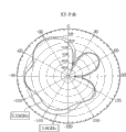
图6A至图6C为图2中双频印刷天线的辐射场型图。6A to 6C are radiation pattern diagrams of the dual-frequency printed antenna in FIG. 2 .
图7为图2中双频印刷天线的辐射效率图。FIG. 7 is a radiation efficiency diagram of the dual-frequency printed antenna in FIG. 2 .
图8到图11为本发明其他实施例的示意图。8 to 11 are schematic diagrams of other embodiments of the present invention.
主要元件符号说明Description of main component symbols
10、20 双频印刷天线10, 20 Dual frequency printed antenna
11、21 基板11, 21 Substrate
12、14、22、24 单极天线12, 14, 22, 24 monopole antenna
13、23 接地金属片13, 23 Ground metal sheet
F1、F2 馈入端F1, F2 Feed-in terminal
S1、S2 侧边S1, S2 side
E1、E2、E3、E4 边缘E1, E2, E3, E4 Edge
具体实施方式 Detailed ways
请参考图1,图1为本发明实施例一双频印刷天线10的示意图。双频印刷天线10用于一多输入多输出无线通信系统(如IEEE 802.11n)的一电子装置,用来进行无线信号的同步收发。双频印刷电路天线10包括一基板11、一单极天线12及一接地金属片13。单极天线12是以一金属线实现的曲折式(meander-line)单极天线,其形成在基板11上,其电气长度近似于一第一频段波长的四分之一,也等于一第二频段波长的四分之三。其中,第二频段的频率高于第一频段的频率。接地金属片13亦形成在基板11上,用来作为单极天线12的一地端。单极天线12的一馈入端F1形成在接地金属片13的一第一侧边S1,并将其分成一第一边缘E1及一第二边缘E2。其中,第一边缘E1及第二边缘E2的长度近似于第二频段波长的四分之一。Please refer to FIG. 1 , which is a schematic diagram of a dual-band printed
为了支持多输入多输出无线通信系统,双频印刷天线10另包括一单极天线14。单极天线14形成在基板11上,具有与单极天线12相同的结构。单极天线14的一馈入端F2形成在接地金属片13的一第二侧边S2,并将其分成一第三边缘E3及一第四边缘E4。其中,第三边缘E3及第四边缘E4的长度近似于第二频段波长的四分之一。In order to support MIMO wireless communication systems, the dual-band printed
如图1所示,第一侧边S1及第二侧边S2为接地金属片13的相对边,而第一边缘E2与第三边缘E3相邻。换句话说,在本发明实施例中,基板11上存在两支单极天线12及14,天线之间以接地金属片13隔开。每一单极天线拥有两个频段:第一频段及第二频段,其分别对应一低频频段与一高频频段。单极天线的电气长度约为低频的四分之一波长,也为高频的四分之三波长。单极天线的馈入端F1及F2分别将接地金属片13的两侧边S1及S2分成两段边缘。每段边缘的长度约为高频的四分之一波长。关于双频印刷天线10的设计原理,请继续参考以下说明。As shown in FIG. 1 , the first side S1 and the second side S2 are opposite sides of the
如本领域具通常知识者所知,中间馈入的二分之一波长偶极天线的输入阻抗实部约为75欧姆(Ω);而非中间馈入的1个波长偶极天线(信号线3/4波长,地线1/4波长)的输入阻抗实部经过模拟,接近100欧姆。假设天线的辐射阻抗为Ra,欧姆损耗电阻为Rohm,则天线的辐射效率正比于Ra/(Ra+Rohm)。由于天线的欧姆损耗电阻大约等于10-3欧姆,因此由偶极天线的辐射效率计算公式可得知,辐射阻抗越大,辐射效率越高。其中,对于单极或偶极天线来说,天线的辐射阻抗又大约正比于天线输入阻抗的实部。As known to those skilled in the art, the real part of the input impedance of a center-fed half-wavelength dipole antenna is about 75 ohms (Ω); rather than a center-fed 1-wavelength dipole antenna (
一般来说,印刷式单极天线受限于基板大小,使其与地端的距离很近,导致辐射阻抗往往很小(约为10欧姆)。在此情形下,在对天线进行阻抗匹配之后,天线的频宽会变得很小。因此,如果能让天线的初始辐射阻抗尽量接近50欧姆,则天线的频宽在进行阻抗匹配之后会增加许多。在本发明实施例中,由于电气长度近似于高频四分之三波长的单极天线及长度近似于高频四分之一波长的地端边缘,类似于非中间馈入的1波长偶极天线,因此可用来增加高频的辐射阻抗,而增加高频频段的频宽。Generally speaking, the printed monopole antenna is limited by the size of the substrate, making it very close to the ground, resulting in a very small radiation impedance (about 10 ohms). In this case, after impedance matching is performed on the antenna, the bandwidth of the antenna becomes very small. Therefore, if the initial radiation impedance of the antenna can be as close as possible to 50 ohms, the bandwidth of the antenna will increase a lot after impedance matching. In the embodiment of the present invention, since the monopole antenna whose electrical length is approximately three-quarters of the high-frequency wavelength and the ground edge whose length is approximately one-fourth the high-frequency wavelength, it is similar to a non-intermediately fed 1-wavelength dipole The antenna, therefore, can be used to increase the radiation impedance of the high frequency, thereby increasing the bandwidth of the high frequency band.
除此之外,单极天线的馈入端F1及F2将接地金属片13分成两段边缘。馈入端F1及F2以下的地边缘长度约为高频的四分之一波长(即边缘E2及E4)。在此处馈入时,高频电流为最大值,频宽也最宽,再加上天线本身为四分之三波长,因此能使高频信号形成谐振。同样地,馈入端F1及F2以上地边缘长度近似于高频频段的1/4波长(即边缘E1及E3),而能使高频信号形成谐振。在此情形下,边缘E1及E3类似一反射器,用来隔离两天线高频频段的地电流,以减少流到邻近天线的电流。如此一来,单极天线12及14具有良好的隔离度。In addition, the feed-in ends F1 and F2 of the monopole antenna divide the
优选地,本发明实施例可视阻抗匹配需求,适当地调整边缘E1及E3的长度,使其略大于高频频段波长的四分之一。如此一来,本发明实施例可进一步增加高频频段的频宽。Preferably, according to the embodiment of the present invention, the lengths of the edges E1 and E3 can be appropriately adjusted according to the requirement of impedance matching, so that they are slightly larger than a quarter of the wavelength of the high-frequency band. In this way, the embodiment of the present invention can further increase the bandwidth of the high frequency band.
请参考图2,图2为本发明优选实施例的一双频印刷天线20的示意图。双频印刷天线20的操作频率为2.4GHz与5GHz,其实现在一支持IEEE802.11n无线局域网络标准的一USB无线网卡(WLAN USB Dongle)中。如图2所示,双频印刷天线20包括两支单极天线22及24。单极天线22及24的天线长度约为2.45GHz的四分之一波长及5.5GHz的四分之三波长。馈入点以下的地边缘长度为5.5GHz的四分之一波长(7.5mm),馈入点以上的地边缘大于5G的1/4波长(11mm)。Please refer to FIG. 2 , which is a schematic diagram of a dual-band printed
关于双频印刷天线20的天线特性模拟结果,请参考图3至图7。图3为双频印刷天线20的史密斯图(Smith Chart),图4为双频印刷天线20的反射系数图,图5为双频印刷天线20的耦合系数(Coupling Coefficient)图,图6A至图6C为双频印刷天线20的辐射场型图,而图7则为双频印刷天线20的辐射效率图。For the antenna characteristic simulation results of the dual-band printed
如图3所示,在高频时,双频印刷天线20的实部阻抗落在传输线的特征阻抗附近,而使高频频带具有很宽的频宽。图4则分别显示了单极天线22及24的反射系数。若以-10dB为基准,双频印刷天线20的低频频宽约落在2.4GHZ~2.6GHz之间,而高频频宽则落在5.15GHz~6GHz之间。As shown in FIG. 3 , at high frequencies, the real part impedance of the dual-frequency printed
图5显示了单极天线22及24之间的耦合系数,其绘制方式为分别将单极天线22及24作为信号输入端及信号输出端,借由测量或模拟由一单极天线传输(或耦合)至另一单极天线的能量比例而获得。由于两支天线馈入点以上的地边缘长度约大于5GHz的四分之一波长,使得5GHz频段的耦合系数都在-15dB以下,因此两支相邻天线在高频频段具有良好的隔离度。Fig. 5 shows the coupling coefficient between
图6A至图6C显示了单极天线22在三个不同切面的辐射场型图。在绘制单极天线22的辐射场型时,本发明实施例将单极天线24耦接50欧姆的负载,以模拟两支天线间的互相干扰的情况。如图6A及图6C所示,由于两天线馈入点以上地边缘会对高频频段信号造成反射,因此,单极天线22在XY平面及YZ平面的辐射场型会被推挤至180-270-360度的半平面,而使得单极天线22及24具有良好的隔离度。在此情形下,双频印刷天线20亦能保持好的辐射效率,在高频频段的辐射效率高达60~80%,如图7所示。6A to 6C show the radiation pattern diagrams of the
请注意,在本发明实施例中,单极天线22及24形成在基板的同一面,而在其他实施例中,单极天线22及24亦可分别形成在基板的上下两面,而不限于此。此外,单极天线及接地金属片的形状、尺寸或材质等亦可根据实际需求进行调整,只要相关电性长度符合本发明的限制,均属本发明的范围。图8到图11为本发明其他实施例的示意图。Please note that in the embodiment of the present invention, the
综上所述,本发明提供一种用于USB无线网络装置的双频印刷电路天线,其利用长度为低频四分之一波长亦为高频四分之三波长的单极天线增加高频信号的频宽,且在多支天线共地的情况下,选择馈入点的位置,使得高频的频段拥有非常好的隔离度、辐射效率与频宽。In summary, the present invention provides a dual-band printed circuit antenna for USB wireless network devices, which utilizes a monopole antenna whose length is 1/4 of the wavelength of the low frequency and 3/4 of the wavelength of the high frequency to increase the high-frequency signal In the case of multiple antennas sharing the same ground, the position of the feed point is selected so that the high frequency band has very good isolation, radiation efficiency and bandwidth.
以上所述仅为本发明的优选实施例,凡依本发明所做的均等变化与修饰,均应属本发明的涵盖范围。The above descriptions are only preferred embodiments of the present invention, and all equivalent changes and modifications made according to the present invention shall fall within the scope of the present invention.
Claims (12)
Priority Applications (1)
| Application Number | Priority Date | Filing Date | Title |
|---|---|---|---|
| CN200910222876XA CN102074786B (en) | 2009-11-19 | 2009-11-19 | Dual frequency printed circuit antenna for electronic devices |
Applications Claiming Priority (1)
| Application Number | Priority Date | Filing Date | Title |
|---|---|---|---|
| CN200910222876XA CN102074786B (en) | 2009-11-19 | 2009-11-19 | Dual frequency printed circuit antenna for electronic devices |
Publications (2)
| Publication Number | Publication Date |
|---|---|
| CN102074786A CN102074786A (en) | 2011-05-25 |
| CN102074786B true CN102074786B (en) | 2013-05-08 |
Family
ID=44033202
Family Applications (1)
| Application Number | Title | Priority Date | Filing Date |
|---|---|---|---|
| CN200910222876XA Expired - Fee Related CN102074786B (en) | 2009-11-19 | 2009-11-19 | Dual frequency printed circuit antenna for electronic devices |
Country Status (1)
| Country | Link |
|---|---|
| CN (1) | CN102074786B (en) |
Families Citing this family (4)
| Publication number | Priority date | Publication date | Assignee | Title |
|---|---|---|---|---|
| CN103427863B (en) * | 2012-05-18 | 2015-08-26 | 宏碁股份有限公司 | communication device |
| CN103441330A (en) * | 2013-08-06 | 2013-12-11 | 华为终端有限公司 | Wireless communication equipment |
| CN103531906B (en) * | 2013-10-24 | 2016-12-07 | 华为终端有限公司 | Mobile device |
| CN109378586B (en) * | 2018-11-28 | 2021-01-29 | 英业达科技有限公司 | Multi-feed antenna |
Citations (3)
| Publication number | Priority date | Publication date | Assignee | Title |
|---|---|---|---|---|
| CN1191633A (en) * | 1995-06-02 | 1998-08-26 | 艾利森公司 | Multiple band printed monopole antenna |
| CN1624974A (en) * | 2003-12-01 | 2005-06-08 | 友旺科技股份有限公司 | Microwire blocking dual-frequency monopole printed antenna and preparation method thereof |
| CN201072805Y (en) * | 2007-03-13 | 2008-06-11 | 中兴通讯股份有限公司 | A dual-band broadband printed antenna |
Family Cites Families (1)
| Publication number | Priority date | Publication date | Assignee | Title |
|---|---|---|---|---|
| KR100625121B1 (en) * | 2003-07-01 | 2006-09-19 | 에스케이 텔레콤주식회사 | Method and Apparatus for Reducing SAR Exposure in a Communication Handset Device |
-
2009
- 2009-11-19 CN CN200910222876XA patent/CN102074786B/en not_active Expired - Fee Related
Patent Citations (3)
| Publication number | Priority date | Publication date | Assignee | Title |
|---|---|---|---|---|
| CN1191633A (en) * | 1995-06-02 | 1998-08-26 | 艾利森公司 | Multiple band printed monopole antenna |
| CN1624974A (en) * | 2003-12-01 | 2005-06-08 | 友旺科技股份有限公司 | Microwire blocking dual-frequency monopole printed antenna and preparation method thereof |
| CN201072805Y (en) * | 2007-03-13 | 2008-06-11 | 中兴通讯股份有限公司 | A dual-band broadband printed antenna |
Also Published As
| Publication number | Publication date |
|---|---|
| CN102074786A (en) | 2011-05-25 |
Similar Documents
| Publication | Publication Date | Title |
|---|---|---|
| TWI420743B (en) | Dual frequency printed circuit antenna for electronic devices | |
| CN1734836B (en) | Antenna | |
| CN102868017B (en) | Radiation device and array antenna based on same | |
| US20100103061A1 (en) | Unidirectional antenna comprising a dipole and a loop | |
| CN104393407B (en) | Metamaterial-based small dual-frequency MIMO antennas | |
| US20090051614A1 (en) | Folded dipole antenna | |
| KR20120138758A (en) | Antennas with novel current distribution and radiation patterns, for enhanced antenna isolation | |
| CN102110900A (en) | Array antenna of mobile terminal and implementation method of array antenna | |
| CN106785370A (en) | A kind of mimo antenna of the high-isolation for mobile terminal | |
| CN101388494B (en) | Multi-antenna integrated module | |
| WO2008000175A1 (en) | Miniature balanced antenna with differential feed | |
| CN107634322B (en) | Double-frequency high-gain omnidirectional antenna | |
| CN106299679B (en) | Antenna and RF signal transceiver | |
| CN102055064A (en) | Circularly polarized antenna for a multiple-input multiple-output wireless communication system | |
| CN103151607B (en) | For the broadband dual-antenna system based on decoupling line structure of mobile terminal | |
| CN108493588A (en) | Indoor base station and its PIFA antennas | |
| CN103367893A (en) | High-isolation broadband two-antenna system | |
| Sarkar et al. | A compact four element CSRR-loaded antenna for dual band pattern diversity MIMO applications | |
| Abdullah et al. | Compact four-port MIMO antenna system at 3.5 GHz | |
| TWI502815B (en) | Dual frequency antenna | |
| CN100414770C (en) | Ultra-Wideband Fractal Antennas Fed by Coplanar Waveguide | |
| CN105406182B (en) | A kind of UWB mimo antennas that notch bandwidth is controllable | |
| CN102074786B (en) | Dual frequency printed circuit antenna for electronic devices | |
| Verma et al. | Design of 2× 2 single sided wrench shaped UWB MIMO antenna with high isolation | |
| CN207116688U (en) | Dual frequency high gain omnidirectional antenna |
Legal Events
| Date | Code | Title | Description |
|---|---|---|---|
| C06 | Publication | ||
| PB01 | Publication | ||
| C10 | Entry into substantive examination | ||
| SE01 | Entry into force of request for substantive examination | ||
| C14 | Grant of patent or utility model | ||
| GR01 | Patent grant | ||
| ASS | Succession or assignment of patent right |
Owner name: LIANFA SCIENCE AND TECHNOLOGY CO., LTD. Free format text: FORMER OWNER: RALINK TECHNOLOGY INC. Effective date: 20140723 |
|
| C41 | Transfer of patent application or patent right or utility model | ||
| TR01 | Transfer of patent right |
Effective date of registration: 20140723 Address after: Hsinchu Science Industrial Park, Taiwan, China Patentee after: MEDIATEK Inc. Address before: Hsinchu County, Taiwan, China Patentee before: RALINK TECHNOLOGY CORP. |
|
| CF01 | Termination of patent right due to non-payment of annual fee |
Granted publication date: 20130508 |
|
| CF01 | Termination of patent right due to non-payment of annual fee |