CN102064697A - System and method for providing linear buck boost transitions within a buck boost converter - Google Patents
System and method for providing linear buck boost transitions within a buck boost converter Download PDFInfo
- Publication number
- CN102064697A CN102064697A CN2010106214542A CN201010621454A CN102064697A CN 102064697 A CN102064697 A CN 102064697A CN 2010106214542 A CN2010106214542 A CN 2010106214542A CN 201010621454 A CN201010621454 A CN 201010621454A CN 102064697 A CN102064697 A CN 102064697A
- Authority
- CN
- China
- Prior art keywords
- signal
- ramp signal
- response
- voltage
- pwm
- Prior art date
- Legal status (The legal status is an assumption and is not a legal conclusion. Google has not performed a legal analysis and makes no representation as to the accuracy of the status listed.)
- Granted
Links
Images


Classifications
-
- H—ELECTRICITY
- H02—GENERATION; CONVERSION OR DISTRIBUTION OF ELECTRIC POWER
- H02M—APPARATUS FOR CONVERSION BETWEEN AC AND AC, BETWEEN AC AND DC, OR BETWEEN DC AND DC, AND FOR USE WITH MAINS OR SIMILAR POWER SUPPLY SYSTEMS; CONVERSION OF DC OR AC INPUT POWER INTO SURGE OUTPUT POWER; CONTROL OR REGULATION THEREOF
- H02M3/00—Conversion of DC power input into DC power output
- H02M3/02—Conversion of DC power input into DC power output without intermediate conversion into AC
- H02M3/04—Conversion of DC power input into DC power output without intermediate conversion into AC by static converters
- H02M3/10—Conversion of DC power input into DC power output without intermediate conversion into AC by static converters using discharge tubes with control electrode or semiconductor devices with control electrode
- H02M3/145—Conversion of DC power input into DC power output without intermediate conversion into AC by static converters using discharge tubes with control electrode or semiconductor devices with control electrode using devices of a triode or transistor type requiring continuous application of a control signal
- H02M3/155—Conversion of DC power input into DC power output without intermediate conversion into AC by static converters using discharge tubes with control electrode or semiconductor devices with control electrode using devices of a triode or transistor type requiring continuous application of a control signal using semiconductor devices only
- H02M3/156—Conversion of DC power input into DC power output without intermediate conversion into AC by static converters using discharge tubes with control electrode or semiconductor devices with control electrode using devices of a triode or transistor type requiring continuous application of a control signal using semiconductor devices only with automatic control of output voltage or current, e.g. switching regulators
- H02M3/158—Conversion of DC power input into DC power output without intermediate conversion into AC by static converters using discharge tubes with control electrode or semiconductor devices with control electrode using devices of a triode or transistor type requiring continuous application of a control signal using semiconductor devices only with automatic control of output voltage or current, e.g. switching regulators including plural semiconductor devices as final control devices for a single load
- H02M3/1582—Buck-boost converters
-
- H—ELECTRICITY
- H02—GENERATION; CONVERSION OR DISTRIBUTION OF ELECTRIC POWER
- H02M—APPARATUS FOR CONVERSION BETWEEN AC AND AC, BETWEEN AC AND DC, OR BETWEEN DC AND DC, AND FOR USE WITH MAINS OR SIMILAR POWER SUPPLY SYSTEMS; CONVERSION OF DC OR AC INPUT POWER INTO SURGE OUTPUT POWER; CONTROL OR REGULATION THEREOF
- H02M3/00—Conversion of DC power input into DC power output
- H02M3/02—Conversion of DC power input into DC power output without intermediate conversion into AC
- H02M3/04—Conversion of DC power input into DC power output without intermediate conversion into AC by static converters
- H02M3/10—Conversion of DC power input into DC power output without intermediate conversion into AC by static converters using discharge tubes with control electrode or semiconductor devices with control electrode
- H02M3/145—Conversion of DC power input into DC power output without intermediate conversion into AC by static converters using discharge tubes with control electrode or semiconductor devices with control electrode using devices of a triode or transistor type requiring continuous application of a control signal
- H02M3/155—Conversion of DC power input into DC power output without intermediate conversion into AC by static converters using discharge tubes with control electrode or semiconductor devices with control electrode using devices of a triode or transistor type requiring continuous application of a control signal using semiconductor devices only
- H02M3/156—Conversion of DC power input into DC power output without intermediate conversion into AC by static converters using discharge tubes with control electrode or semiconductor devices with control electrode using devices of a triode or transistor type requiring continuous application of a control signal using semiconductor devices only with automatic control of output voltage or current, e.g. switching regulators
- H02M3/157—Conversion of DC power input into DC power output without intermediate conversion into AC by static converters using discharge tubes with control electrode or semiconductor devices with control electrode using devices of a triode or transistor type requiring continuous application of a control signal using semiconductor devices only with automatic control of output voltage or current, e.g. switching regulators with digital control
Landscapes
- Engineering & Computer Science (AREA)
- Power Engineering (AREA)
- Dc-Dc Converters (AREA)
Abstract
一种电压调节器,包括用于响应于输入电压和多个开关控制信号产生输出电压的第一电路。开关控制电路响应于输出电压与降压斜坡信号和升压斜坡信号中的至少一个产生开关控制信号。电压斜坡产生电路产生降压斜坡信号和升压斜坡信号中的每一个。升压斜坡信号包括被偏移降压斜坡信号的峰值的降压斜坡信号。
A voltage regulator includes a first circuit for generating an output voltage in response to an input voltage and a plurality of switch control signals. The switch control circuit generates a switch control signal in response to the output voltage and at least one of a buck ramp signal and a boost ramp signal. A voltage ramp generating circuit generates each of a buck ramp signal and a boost ramp signal. The boost ramp signal includes a buck ramp signal offset by a peak value of the buck ramp signal.
Description
相关申请的交叉引用 Cross References to Related Applications
本申请是2009年4月24日提交的题为“用于在降升压转换器中提供线性降升压转换的系统和方法(SYSTEM AND METHOD FOR PROVIDING LINEAR BUCK BOOST TRANSITIONS WITHIN A BUCK BOOST CONVERTER)”的美国专利申请No.12/429241的部分继续申请,该申请No.12/429241要求2008年10月6日提交的题为“降升压转换(BUCK-BOOST TRANSITION)”的美国临时专利申请No.61/103103的优先权,上述专利通过引用结合于此。 This application is filed on April 24, 2009 and is entitled "SYSTEM AND METHOD FOR PROVIDING LINEAR BUCK BOOST TRANSITIONS WITHIN A BUCK BOOST CONVERTER" A continuation-in-part of U.S. Patent Application No. 12/429241, which claims U.S. Provisional Patent Application No. Priority of .61/103103, the above patent is hereby incorporated by reference. the
技术领域technical field
本发明涉及降升压转换器,更具体地涉及用于控制降升压转换器操作以提供降压和升压操作模式之间的线性转换的系统和方法。 The present invention relates to buck-boost converters, and more particularly to systems and methods for controlling the operation of a buck-boost converter to provide a linear transition between buck and boost modes of operation. the
背景技术Background technique
在许多电池供电的系统中,可能发生输入电压下降到低于输出电压的情况。当这种情况发生时,为了给系统提供调节功率,除降压转换器之外还需要升压转换器。当使用降升压转换器时,从升压操作模式到降压操作模式的转换和从降压操作模式到升压操作模式的转换是非线性的。这将引起在降升压调节器的输出处发生超调或欠调电压情况。因此,需要提供某种用于降升压调节器的控制机构,来提供更线性的操作特性并且实质上避免超调或欠调电压的问题。 In many battery-powered systems, it can happen that the input voltage drops below the output voltage. When this happens, a boost converter is required in addition to the buck converter in order to provide regulated power to the system. When using a buck-boost converter, the transition from boost to buck mode of operation and from buck to boost mode of operation is non-linear. This will cause an overshoot or undershoot voltage condition at the output of the buck-boost regulator. Therefore, there is a need to provide some kind of control mechanism for a buck-boost regulator that provides a more linear operating characteristic and substantially avoids the problems of overshooting or undershooting the voltage. the
发明内容Contents of the invention
如本文公开和描述的本发明在其中一个方面包括一种电压调节器,其包括用于响应于多个开关控制信号中的输入电压产生输出电压的第一电路。开关控制电路响应于在降压斜坡信号和升压斜坡信号中的至少一个中的输出电压产生开关控制信号。电压斜坡产生电路产生降压斜坡信号和升压斜坡信号中的每一 个。升压斜坡信号包括以降压斜坡信号的峰值进行偏移的降压斜坡信号。 The invention as disclosed and described herein includes, in one aspect, a voltage regulator including a first circuit for generating an output voltage in response to an input voltage in a plurality of switch control signals. The switch control circuit generates a switch control signal responsive to the output voltage in at least one of the buck ramp signal and the boost ramp signal. A voltage ramp generating circuit generates each of a buck ramp signal and a boost ramp signal. The boost ramp signal includes a buck ramp signal offset by the peak value of the buck ramp signal. the
附图说明Description of drawings
为了更全面地理解,现结合附图参考以下描述,在附图中: For a more complete understanding, reference is now made to the following description in conjunction with the accompanying drawings, in which:
图1a是降升压转换器的示意图; Figure 1a is a schematic diagram of a buck-boost converter;
图1b图示了用于响应于斜坡信号和补偿信号产生PWM信号和驱动信号的电路; Figure 1b illustrates a circuit for generating a PWM signal and a drive signal in response to a ramp signal and a compensation signal;
图2图示了标准降压斜坡控制器的波形; Figure 2 illustrates the waveforms of a standard buck ramp controller;
图3图示了当输出电压降低或者输入电压降低时降压斜坡控制器的波形; Figure 3 illustrates the waveform of the buck ramp controller when the output voltage decreases or the input voltage decreases;
图4图示了在降升压转换器的升压操作模式中产生斜坡信号的方法; Figure 4 illustrates a method of generating a ramp signal in a boost mode of operation of a buck-boost converter;
图5是用于降升压转换器的降压和升压操作模式的斜坡产生器的功能框图; Figure 5 is a functional block diagram of a ramp generator for buck and boost modes of operation of a buck-boost converter;
图6图示了用来驱动降升压转换器的控制器和驱动电路; Figure 6 illustrates the controller and drive circuit used to drive the buck-boost converter;
图7图示了当输入从6伏变为4伏时用于降升压转换器的PWM驱动电路的输出电压; Figure 7 illustrates the output voltage of a PWM drive circuit for a buck-boost converter when the input changes from 6 volts to 4 volts;
图8图示了降升压转换器使用图4的斜坡产生器从降压操作模式到升压操作模式的转换; Figure 8 illustrates the transition of a buck-boost converter from a buck mode of operation to a boost mode of operation using the ramp generator of Figure 4;
图9图示了用于使用附图4的斜坡产生器的降升压转换器的从升压操作模式到降压操作模式的转换; Figure 9 illustrates a transition from a boost mode of operation to a buck mode of operation for a buck-boost converter using the ramp generator of Figure 4;
图10图示了升降压模式之间的PWM驱动信号,其中输入电压V输入大约等于输出电压V输出; Figure 10 illustrates the PWM drive signals between buck-boost modes, where the input voltage Vin is approximately equal to the output voltage Vout;
图11图示了在升降压操作模式期间的输出电压,其中输入电压V输入约等于输出电压V输出;以及 Figure 11 illustrates the output voltage during a buck-boost mode of operation, where the input voltage Vin is approximately equal to the output voltage Vout ; and
图12图示了响应电流控制模式中的移位斜坡电压产生降压PWM信号和升压PWM信号的替代实施例。 FIG. 12 illustrates an alternate embodiment of generating a buck PWM signal and a boost PWM signal in response to a shifted ramp voltage in current control mode. the
具体实施方式Detailed ways
现参考附图,其中这里使用的相同的附图标记始终表示相同的元件,示出和描述了用于在降升压转换器提供线性降升压转换的系统和方法的多个视图和实施例,并且描述了其他可能的实施例。附图不一定按照比例绘制,并且在一些实例中仅为了图示说明的目的在适当的位置将附图夸大和/或简化。本领域技 术人员基于可行实施例的以下示例将得知许多可能的应用和变型。 Referring now to the drawings, wherein like reference numerals are used herein to refer to like elements throughout, there are shown and described various views and embodiments of a system and method for providing linear buck-boost conversion in a buck-boost converter , and other possible embodiments are described. The figures are not necessarily to scale and are in some instances exaggerated and/or simplified where appropriate for illustrative purposes only. Many possible applications and variants will become apparent to those skilled in the art based on the following example of a possible embodiment. the
在许多电池供电的系统中,可能发生输入电压下降到低于输出电压的情况。当该情况发生时,除降压转换器之外还需要升压转换器,来给系统提供经调节功率。当使用降升压转换器时,从升压操作模式到降压操作模式的转换和相反的转换是非线性的。这可能引起在降升压调节器的输出处发生超调或欠调电压情况。因此,需要提供某种用于降升压调节器的控制机构,其能提供更线性的操作特性并且实质上避免了出现超调或欠调电压的问题。许多现行的解决方案使用调节器的输入电压和输出电压来确定降压和升压操作模式的转换点。此外,这些解决方案围绕这些瞬时点设立窗口,其中在全桥结构中使用降升压转换器的所有四个开关。 In many battery-powered systems, it can happen that the input voltage drops below the output voltage. When this occurs, a boost converter is required in addition to the buck converter to provide regulated power to the system. When using a buck-boost converter, the transition from boost mode of operation to buck mode of operation and vice versa is non-linear. This can cause an overshoot or undershoot voltage condition at the output of the buck-boost regulator. Therefore, there is a need to provide some kind of control mechanism for a buck-boost regulator that provides a more linear operating characteristic and substantially avoids the problems of voltage overshoot or undershoot. Many current solutions use the regulator's input and output voltages to determine the transition points between buck and boost modes of operation. Furthermore, these solutions window around these instantaneous points, where all four switches of the buck-boost converter are used in a full-bridge configuration. the
现参考图1,该图示出降升压转换器102和关联的开关控制电路104的示意图。V输入处的输入电压通过开关晶体管108被应用到节点106。开关晶体管108被连接在节点106和节点110之间。第二晶体管112被连接在节点110和接地节点114之间。电感器116被连接在节点110和节点118之间。晶体管120被连接在节点118和接地之间。第四晶体管122被连接在节点118和节点124之间,并且输出电容126被连接在节点124和接地之间。节点124包括提供输出电压V输出的输出电压节点。开关控制电路104从输出电压节点124接收输出电压V输出作为反馈,并且使用该信息分别为降升压调节器的每一个晶体管108、112、120和122产生开关控制信号S1、S2、S3和S4。 Referring now to FIG. 1 , a schematic diagram of a buck-
现参考附图1b,示出了用于为开关控制器104中的降升压转换器的开关的驱动电路产生PWM开关信号的电路。误差放大器140响应于来自输出电压节点124的输出电压V输出和基准电压VREF产生补偿信号。误差放大器140提供的补偿信号被提供到PWM比较器142的非反相输入端。PWM比较器142的反相输入端接收斜坡信号,并且响应于斜坡信号和来自误差放大器140的补偿信号产生输入驱动电路144的PWM信号。正如下面所述,这个电路可被用于产生降压或升压PWM信号,。驱动电路144响应于PWM信号为降升压调节器的各个开关晶体管产生驱动信号。 Referring now to FIG. 1 b , there is shown a circuit for generating PWM switching signals for the driving circuit of the switches of the buck-boost converter in the
图2示出设置在开关控制器104中的标准降压斜坡控制器信号。所产生的降压斜坡202与输出补偿器信号COMP OUT 204一起使用以产生降压PWM驱动信号208。例如,该补偿器信号可包括误差放大器140的输出,正如上面所述。 正如所看到地,当降压斜坡信号202下降到低于点206处的补偿器信号204,降压PWM信号208变为逻辑“高”电平。当降压斜坡信号202高于补偿器信号204,正如其在点210处,降压PWM信号208降低到逻辑“低”电平。 FIG. 2 shows a standard buck ramp controller signal provided in
现参考附图3,示出了当降压转换器的输出电压开始降低或者输入电压开始降低时呈现的降压斜坡202、补偿器信号204和降压PWM信号208。正如所看到地,当补偿器信号204上升到高于降压斜坡信号峰值302时,降压PWM信号208的脉宽如点304与306之间所示地增加。这是因为当补偿器输出信号204高于斜坡信号峰值302时PWM信号208变为逻辑“高”电平的事实而引起的。当补偿器信号204降低并且再一次与降压斜坡信号202在点308处相交时,可确定降压斜坡信号202目前高于补偿器信号204,并且降压PWM信号208在306处下降至逻辑低电平。一旦补偿器信号204下降到低于降压斜坡信号202的峰值302,降压PWM输出208以与关于附图2的前面描述相似的方法操作,其中当降压斜坡信号202低于补偿器输出时降压PWM信号208变为逻辑“高”电平,而当降压斜坡信号202高于补偿器输出204时降压PWM信号208变为逻辑“低”电平。 Referring now to FIG. 3 , there is shown a
当降压调节器的输入电压下降到低于输出电压时,需要升压转换器。然而,从降压到升压的转换是非线性的,并且可能引起在电路中欠调或超调电压情况的发生。这里下面描述的本发明解决方案通过使用补偿器信号来克服超调或欠调的问题以实现线性转换。升压斜坡电压信号被设计以使得当输入电压开始降低时,降压转换器的占空比将增加,但是在一些点上输入电压将如附图2所示高于降压信号斜坡峰值。如果输入电压继续下降,在降压占空比达到100%之后,并且升压操作模式没有被激活,那么转换器的输出电压将开始下降。这将引起补偿信号204继续增加。 A boost converter is required when the input voltage to the buck regulator drops below the output voltage. However, the transition from buck to boost is non-linear and can cause voltage undershoot or overshoot conditions to occur in the circuit. The inventive solution described here below overcomes the problem of overshoot or undershoot by using the compensator signal to achieve linear conversion. The boost ramp voltage signal is designed so that when the input voltage starts to decrease, the duty cycle of the buck converter will increase, but at some point the input voltage will be higher than the buck signal ramp peak as shown in Figure 2. If the input voltage continues to drop, after the buck duty cycle reaches 100%, and the boost mode of operation is not activated, then the output voltage of the converter will start to drop. This will cause the
为了克服这个问题,正如图4更全面地图示,升压斜坡电压402通过将降压斜坡电压偏移一个DC电压电平来产生,该DC电压电平等于用于降压操作模式的降压斜坡电压的峰值。这个DC偏移升压斜坡电压402在升降压转换或降升压转换期间被用于升压斜坡信号,以使转换器的操作能够保持线性。当补偿器信号204高于降压斜坡信号202时,正如以上关于图3所描述地,降压PWM信号可保持在逻辑高电平以提供非线性操作。通过将升压斜坡信号402与补偿器输出204一起使用来代替降压斜坡信号202,可产生具有线性特性的升压 PWM信号404。在这种情况下,当升压斜坡信号402下降到低于补偿器输出204时,升压PWM信号404在点406处变为逻辑高电平。相似地,当升压斜坡信号402在点408处上升到高于补偿器信号204时,升压PWM信号404变为逻辑低电平。 To overcome this problem, as illustrated more fully in FIG. 4 , the
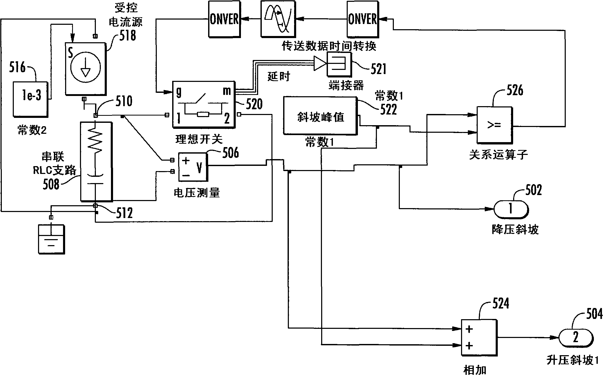
现参考附图5,示出了用于产生斜坡信号的电路的框图,该斜坡信号用于在降压和升压操作模式以产生图4所示波形。在节点502处提供降压斜坡信号输出208。在节点504处提供升压斜坡信号。在节点502处由电压测量电路506提供降压斜坡信号。电压测量电路测量由与电容器串联的电阻器组成的串联RLC支路508两端的电压。串联RLC支路508被连接在节点510和节点512之间。受控电流源514被连接到节点510,并且接收从存储常数到存储位置516的输入。受控电流源518被附加地连接到接地节点512。理想开关520被连接在节点510和节点512之间。理想开关520提供输出至端接器521的传送数据类型传输延时。理想开关520从通过数据转换提供的关系运算子526接收输入。降压斜坡信号斜坡峰值在522处被确定并被提供到关系运算子526,该关系运算子526确定斜坡峰值是否大于或等于由电压测量电路506测得的包括斜坡电压的电压测量值。加法电路524将存储在位置522中的斜坡峰值DC偏移与由电压测量电路506提供的降压斜坡信号相加,以在节点504处产生升压斜坡信号。以此方式,升压斜坡信号等于降压斜坡信号加上所需的峰值DC偏移。 Referring now to FIG. 5 , there is shown a block diagram of a circuit for generating a ramp signal for use in buck and boost modes of operation to generate the waveforms shown in FIG. 4 . Buck
现参考图6,示出了与图5所描述的斜坡产生电路一起使用的控制器和驱动电路。来自节点502的降压斜坡信号被提供到第一关系运算子606。来自节点504的升压斜坡信号被提供到第二关系运算子608。关系运算子606和608包括大于或等于关系运算。补偿信号204在节点610处被提供,以使得补偿信号可与降压斜坡波形和升压斜坡波形二者比较。如果补偿信号大于降压斜坡信号,则升压斜坡信号被用于驱动升压转换器驱动电路604。如果补偿信号不大于降压斜坡信号,则降压斜坡信号被用于驱动降压驱动电路602。这样,利用在节点610处将补偿信号与降压斜坡和升压斜坡信号的比较,可实现在降压驱动电路602和升压驱动电路604之间的切换期间的线性操作。 Referring now to FIG. 6 , there is shown a controller and driver circuit for use with the ramp generation circuit described in FIG. 5 . The buck ramp signal from
现参考图7-11,示出了各种仿真结果,这些结果说明线性补偿器输出的使用提供了不需要知道输入电压电平的从降压到升压和从升压到降压的转换,而其他方法则需要知道输入电压电平。该系统的一个主要优点是在一个时刻时仅 使用两个开关,而不是现有技术实现中所需的四个,因此提供全面的效率改善。 Referring now to Figures 7-11, various simulation results are shown illustrating that the use of the linear compensator output provides buck-to-boost and boost-to-buck transitions that do not require knowledge of the input voltage level, Other methods require knowledge of the input voltage level. A major advantage of this system is that only two switches are used at a time, instead of the four required in prior art implementations, thus providing an overall efficiency improvement. the
图7示出了当降升压电路从大致由部分702和704所示出的降压操作模式切换到大致由部分706所示出的升压操作模式时,由线708所示的输入电压在从降压操作模式切换到升压操作模式并返回时开始降低或者升高。由线710表示的输出电压保持相对线性。 FIG. 7 shows the input voltage shown by
图8示出了降压和升压操作模式之间的多次转换,其中降压模式大致在808处示出,而升压模式大致在806处示出。在这个操作期间,不论输入电压804是否增加,输出电压802都保持线性。 FIG. 8 shows multiple transitions between buck and boost modes of operation, with buck mode shown generally at 808 and boost mode shown generally at 806 . During this operation, the
图9示出了从升压操作模式到降压操作模式的转换。正如所看到的,在转换期间,不论输入电压804是否减少,输出电压902都保持线性。 Figure 9 shows the transition from boost mode of operation to buck mode of operation. As can be seen, during the transition, the
图10示出了在升压/降压模式期间的PWM驱动,其中V输入基本上等于V输出。线1002示出了在该图底部示出的升压和降压模式之间的转换期间输出电压和输入电压保持线性。 Figure 10 shows PWM drive during boost/buck mode, where Vin is substantially equal to Vout .
图11示出了在升压和降压操作模式期间输出电压以相对线性的方式随着时间振荡的方式。 Figure 11 shows the manner in which the output voltage oscillates over time in a relatively linear fashion during the boost and buck modes of operation. the
通过实现所提出的斜坡转换方案,在升压和降压操作模式之间的转换变得更线性,并且仅依靠实质上是线性的补偿器输出。另外,电路仅要求在升压和降压转换器中使用两个开关,而不是在现有技术方法中所需的四个。 By implementing the proposed ramp transition scheme, the transition between boost and buck modes of operation becomes more linear and only relies on the compensator output being substantially linear. Additionally, the circuit requires only two switches in the boost and buck converters instead of the four required in prior art approaches. the
现参考附图12,示出了用于在电流控制模式中通过降压升压电压调节器中的开关控制电路104(图1)产生降压PWM和升压PWM信号的可选实施例。所添加的对电压调节器斜坡电压的I_BUCK和I_BOOST控制被用于电压调节器的电流模式控制的情况。I_BOOST电流和I_BUCK电流分别包括流过升压侧的低侧开关的电流和流过降压侧的高侧开关的电流。降压斜坡电压1202被应用到加法器电路1204的第一输入端。降压电流(I_BUCK)1206被应用到加法器电路1204的第二输入端。电流I_BUCK 1206可以采用三种方法来测量。这三种方法中的每一种要求当进行测量时上侧降压开关108(图1)导通。I_BUCK电流1206是在降升压调节器的电感器116上测得的。可选地,I_BUCK电流1206可在与晶体管108串联的电阻器上测得。最终,I_BUCK电流测量1206是在上侧降压开关晶体管108上测得的。 Referring now to FIG. 12 , an alternative embodiment for generating buck PWM and boost PWM signals in current control mode by switch control circuit 104 ( FIG. 1 ) in a buck-boost voltage regulator is shown. The added I_BUCK and I_BOOST control of the voltage regulator ramp voltage is used in the case of current mode control of the voltage regulator. The I_BOOST current and the I_BUCK current respectively include the current flowing through the low-side switch on the boost side and the current flowing through the high-side switch on the buck side.
加法器电路1204的输出被提供到比较器1208。比较器1208的另一个输入 端接收来自电压调节器的误差放大器的补偿信号COMP。比较器1208的输出被用于在输出1210处产生降压PWM信号。加法器1204的输出也被施加到第二加法器电路1212的输入端。加法器1212的其他输入端被连接以接收可编程电平移动1214和I_BOOST电流1216。可编程电平移动1214包括斜坡电压被移位的可编程电平。I_BOOST电流1216包括升压电流,并且当下侧升压开关晶体管120导通时可以通过三种方式来测量。当下侧升压开关晶体管120导通时,I_BOOST电流可在电感器116上、与晶体管120串联的电阻器上、或者下侧升压开关晶体管120上测得。来自加法器1212的移位斜坡信号的输出被施加到比较器1218的输入端。比较器1218的其他输入被连接以接收来自误差放大器的补偿信号COMP。比较器1218的输出在输出1220处提供升压PWM信号。 The output of
获得本公开内容的益处的本领域技术人员将理解,本系统和方法用于在降升压转换器中提供线性降升压转换。应理解这里的附图和详细描述被看作是说明性的而非限制性的,并且不旨在被限制为所公开的特定形式和示例。反之,所包括的是对本领域技术人员显而易见的任何进一步的修改、变化、重新安排、替换、替代方案、设计选择以及实施例,而不背离如所附权利要求所限定的本文中的精神和范围,。因此,所附权利要求旨在被解释为包括所有这些进一步的修改、变化、重新安排、替换、替代方案、设计选择以及实施例。 Those skilled in the art having the benefit of this disclosure will appreciate that the present systems and methods are used to provide linear buck-boost conversion in a buck-boost converter. It should be understood that the drawings and detailed description herein are to be regarded as illustrative rather than restrictive, and are not intended to be limited to the particular forms and examples disclosed. Rather, any further modifications, changes, rearrangements, substitutions, alternatives, design choices, and embodiments apparent to those skilled in the art are included without departing from the spirit and scope herein as defined by the appended claims ,. Accordingly, the appended claims are intended to be interpreted to embrace all such further modifications, changes, rearrangements, replacements, alternatives, design choices, and embodiments. the
Claims (18)
Applications Claiming Priority (2)
| Application Number | Priority Date | Filing Date | Title |
|---|---|---|---|
| US12/611,668 US8232789B2 (en) | 2008-10-06 | 2009-11-03 | System and method for providing linear buck boost transitions within a buck boost converter |
| US12/611,668 | 2009-11-03 |
Publications (2)
| Publication Number | Publication Date |
|---|---|
| CN102064697A true CN102064697A (en) | 2011-05-18 |
| CN102064697B CN102064697B (en) | 2016-01-20 |
Family
ID=43927301
Family Applications (1)
| Application Number | Title | Priority Date | Filing Date |
|---|---|---|---|
| CN201010621454.2A Active CN102064697B (en) | 2009-11-03 | 2010-11-03 | For providing the system and method linearly falling boost conversion in falling-rising pressure converter |
Country Status (4)
| Country | Link |
|---|---|
| US (1) | US8232789B2 (en) |
| CN (1) | CN102064697B (en) |
| DE (1) | DE102010060332A1 (en) |
| TW (1) | TWI430543B (en) |
Cited By (10)
| Publication number | Priority date | Publication date | Assignee | Title |
|---|---|---|---|---|
| US9389617B2 (en) | 2013-02-19 | 2016-07-12 | Nvidia Corporation | Pulsed current sensing |
| US9395738B2 (en) | 2013-01-28 | 2016-07-19 | Nvidia Corporation | Current-parking switching regulator with a split inductor |
| US9459635B2 (en) | 2013-02-08 | 2016-10-04 | Nvidia Corporation | Current-parking switching regulator upstream controller |
| US9639102B2 (en) | 2013-02-19 | 2017-05-02 | Nvidia Corporation | Predictive current sensing |
| US9800158B2 (en) | 2013-01-30 | 2017-10-24 | Nvidia Corporation | Current-parking switching regulator downstream controller |
| US9804621B2 (en) | 2013-02-05 | 2017-10-31 | Nvidia Corporation | Current-parking switching regulator downstream controller pre-driver |
| CN108494253A (en) * | 2014-10-10 | 2018-09-04 | 英特希尔美国公司 | Lagging current pattern buck-boost controls framework |
| CN111082657A (en) * | 2018-10-18 | 2020-04-28 | 圣邦微电子(北京)股份有限公司 | Buck-boost converter and control method |
| CN112689947A (en) * | 2018-09-13 | 2021-04-20 | 微芯片技术股份有限公司 | Control of four-switch, single-inductor, non-inverting buck-boost converter |
| CN114765417A (en) * | 2021-01-13 | 2022-07-19 | 上海南芯半导体科技股份有限公司 | Control method and circuit for improving mode switching output stability of buck-boost converter |
Families Citing this family (6)
| Publication number | Priority date | Publication date | Assignee | Title |
|---|---|---|---|---|
| US20100085027A1 (en) * | 2008-10-06 | 2010-04-08 | Intersil Americas Inc. | System and method for providing linear buck boost transitions within a buck boost converter |
| US10637357B1 (en) | 2017-12-20 | 2020-04-28 | Renesas Electronics America Inc. | Ramp offset compensation circuit in a buck boost converter |
| US10594218B1 (en) | 2017-12-20 | 2020-03-17 | Renesas Electronics America Inc. | Hysteresis timing scheme for mode transition in a buck boost converter |
| TWI681613B (en) * | 2018-02-02 | 2020-01-01 | 茂達電子股份有限公司 | Voltage converter for simulating inductor current control |
| US11183935B2 (en) | 2019-03-14 | 2021-11-23 | Microchip Technology Incorporated | Current control for buck-boost converters using conditional offsets |
| WO2023229218A1 (en) * | 2022-05-27 | 2023-11-30 | 삼성전자주식회사 | Method for controlling voltage supplied to rf transmission/reception module, and electronic device for carrying out same |
Citations (4)
| Publication number | Priority date | Publication date | Assignee | Title |
|---|---|---|---|---|
| CN1960145A (en) * | 2005-10-14 | 2007-05-09 | 美国芯源系统股份有限公司 | Switching regulator with automatic multi mode conversion |
| US20080136395A1 (en) * | 2006-11-20 | 2008-06-12 | Bennett Paul T | Methods and apparatus for a spread spectrum switching regulator |
| WO2009033924A2 (en) * | 2007-09-11 | 2009-03-19 | Siemens Ag Österreich | Method for regulating a dc-to-dc converter |
| US20100085027A1 (en) * | 2008-10-06 | 2010-04-08 | Intersil Americas Inc. | System and method for providing linear buck boost transitions within a buck boost converter |
Family Cites Families (4)
| Publication number | Priority date | Publication date | Assignee | Title |
|---|---|---|---|---|
| US4395675A (en) | 1981-10-22 | 1983-07-26 | Bell Telephone Laboratories, Incorporated | Transformerless noninverting buck boost switching regulator |
| US6087816A (en) | 1999-06-29 | 2000-07-11 | Maxim Integrated Products, Inc. | Step-up/step-down switching regulators and pulse width modulation control therefor |
| US6166527A (en) * | 2000-03-27 | 2000-12-26 | Linear Technology Corporation | Control circuit and method for maintaining high efficiency in a buck-boost switching regulator |
| US7902807B2 (en) * | 2008-07-22 | 2011-03-08 | Texas Instruments Incorporated | Multiple switch node power converter control scheme that avoids switching sub-harmonics |
-
2009
- 2009-11-03 US US12/611,668 patent/US8232789B2/en active Active
-
2010
- 2010-11-03 CN CN201010621454.2A patent/CN102064697B/en active Active
- 2010-11-03 DE DE102010060332A patent/DE102010060332A1/en not_active Ceased
- 2010-11-03 TW TW099137747A patent/TWI430543B/en active
Patent Citations (4)
| Publication number | Priority date | Publication date | Assignee | Title |
|---|---|---|---|---|
| CN1960145A (en) * | 2005-10-14 | 2007-05-09 | 美国芯源系统股份有限公司 | Switching regulator with automatic multi mode conversion |
| US20080136395A1 (en) * | 2006-11-20 | 2008-06-12 | Bennett Paul T | Methods and apparatus for a spread spectrum switching regulator |
| WO2009033924A2 (en) * | 2007-09-11 | 2009-03-19 | Siemens Ag Österreich | Method for regulating a dc-to-dc converter |
| US20100085027A1 (en) * | 2008-10-06 | 2010-04-08 | Intersil Americas Inc. | System and method for providing linear buck boost transitions within a buck boost converter |
Cited By (14)
| Publication number | Priority date | Publication date | Assignee | Title |
|---|---|---|---|---|
| US9395738B2 (en) | 2013-01-28 | 2016-07-19 | Nvidia Corporation | Current-parking switching regulator with a split inductor |
| US9800158B2 (en) | 2013-01-30 | 2017-10-24 | Nvidia Corporation | Current-parking switching regulator downstream controller |
| US9804621B2 (en) | 2013-02-05 | 2017-10-31 | Nvidia Corporation | Current-parking switching regulator downstream controller pre-driver |
| US9459635B2 (en) | 2013-02-08 | 2016-10-04 | Nvidia Corporation | Current-parking switching regulator upstream controller |
| TWI691824B (en) * | 2013-02-19 | 2020-04-21 | 輝達公司 | Electric power conversion device and method for estimating current |
| US9639102B2 (en) | 2013-02-19 | 2017-05-02 | Nvidia Corporation | Predictive current sensing |
| US9389617B2 (en) | 2013-02-19 | 2016-07-12 | Nvidia Corporation | Pulsed current sensing |
| CN108494253A (en) * | 2014-10-10 | 2018-09-04 | 英特希尔美国公司 | Lagging current pattern buck-boost controls framework |
| US10804801B2 (en) | 2014-10-10 | 2020-10-13 | Intersil Americas LLC | Hysteretic current mode buck-boost control architecture having sequential switching states |
| CN108494253B (en) * | 2014-10-10 | 2021-06-01 | 英特希尔美国公司 | Hysteretic current mode buck-boost control architecture |
| CN112689947A (en) * | 2018-09-13 | 2021-04-20 | 微芯片技术股份有限公司 | Control of four-switch, single-inductor, non-inverting buck-boost converter |
| CN112689947B (en) * | 2018-09-13 | 2024-04-19 | 微芯片技术股份有限公司 | Control of a four-switch, single inductor, non-inverting buck-boost converter |
| CN111082657A (en) * | 2018-10-18 | 2020-04-28 | 圣邦微电子(北京)股份有限公司 | Buck-boost converter and control method |
| CN114765417A (en) * | 2021-01-13 | 2022-07-19 | 上海南芯半导体科技股份有限公司 | Control method and circuit for improving mode switching output stability of buck-boost converter |
Also Published As
| Publication number | Publication date |
|---|---|
| US8232789B2 (en) | 2012-07-31 |
| TW201141024A (en) | 2011-11-16 |
| TWI430543B (en) | 2014-03-11 |
| US20100085028A1 (en) | 2010-04-08 |
| CN102064697B (en) | 2016-01-20 |
| DE102010060332A1 (en) | 2011-06-01 |
Similar Documents
| Publication | Publication Date | Title |
|---|---|---|
| CN102064697B (en) | For providing the system and method linearly falling boost conversion in falling-rising pressure converter | |
| US8901908B2 (en) | Methods and apparatus for DC-DC conversion using digitally controlled adaptive pulse frequency modulation | |
| JP5853153B2 (en) | Buck-boost converter | |
| EP3136576A2 (en) | Buck-boost converter and method for controlling buck-boost converter | |
| CN105322793A (en) | Cascaded buck-boost DC to DC converter and circuit and method for controlling converter | |
| JP5479940B2 (en) | Buck-boost DC-DC converter and vehicular lamp | |
| CN103516203B (en) | DC-DC controller and operation method thereof | |
| US12483134B2 (en) | Buck converter circuit with seamless PWM/PFM transition | |
| US6946823B2 (en) | Delta-sigma DC-to-DC converter and method thereof | |
| TW201914190A (en) | Control circuit operating in pulse skip mode (psm) and voltage converter having the same | |
| CN114337230B (en) | Soft Start Method for Switching Regulator | |
| CN102751864B (en) | Cuk based current source | |
| JP2010279138A (en) | Switching boost type DC-DC converter and semiconductor integrated circuit device | |
| US7795930B2 (en) | Drive control apparatus for controlling drive of inductive load and drive control method for controlling the same | |
| US8912724B2 (en) | LED emitting device and driving method thereof | |
| JP2011182482A (en) | Switching step-up type dc-dc converter and semiconductor integrated circuit device | |
| CN114257088A (en) | Voltage conversion circuit and power converter | |
| US20100085027A1 (en) | System and method for providing linear buck boost transitions within a buck boost converter | |
| JP5199019B2 (en) | Buck-boost DC-DC converter | |
| JP2012034516A (en) | Operation mode switching type dc-dc converter | |
| US11081957B2 (en) | Power converter with multi-mode timing control | |
| JP4835064B2 (en) | DC-DC converter | |
| TWI405392B (en) | Voltage converter | |
| CN111585435B (en) | Control circuit of voltage converter and voltage converter | |
| JP5109920B2 (en) | Switching power supply |
Legal Events
| Date | Code | Title | Description |
|---|---|---|---|
| C06 | Publication | ||
| PB01 | Publication | ||
| C10 | Entry into substantive examination | ||
| SE01 | Entry into force of request for substantive examination | ||
| C14 | Grant of patent or utility model | ||
| GR01 | Patent grant |