CN102016762B - Ground guard for capacitive sensing - Google Patents
Ground guard for capacitive sensing Download PDFInfo
- Publication number
- CN102016762B CN102016762B CN200980114531.0A CN200980114531A CN102016762B CN 102016762 B CN102016762 B CN 102016762B CN 200980114531 A CN200980114531 A CN 200980114531A CN 102016762 B CN102016762 B CN 102016762B
- Authority
- CN
- China
- Prior art keywords
- line
- many
- bus
- row
- polygonal
- Prior art date
- Legal status (The legal status is an assumption and is not a legal conclusion. Google has not performed a legal analysis and makes no representation as to the accuracy of the status listed.)
- Expired - Fee Related
Links
Images


Classifications
-
- G—PHYSICS
- G06—COMPUTING OR CALCULATING; COUNTING
- G06F—ELECTRIC DIGITAL DATA PROCESSING
- G06F3/00—Input arrangements for transferring data to be processed into a form capable of being handled by the computer; Output arrangements for transferring data from processing unit to output unit, e.g. interface arrangements
- G06F3/01—Input arrangements or combined input and output arrangements for interaction between user and computer
- G06F3/03—Arrangements for converting the position or the displacement of a member into a coded form
- G06F3/041—Digitisers, e.g. for touch screens or touch pads, characterised by the transducing means
- G06F3/044—Digitisers, e.g. for touch screens or touch pads, characterised by the transducing means by capacitive means
- G06F3/0443—Digitisers, e.g. for touch screens or touch pads, characterised by the transducing means by capacitive means using a single layer of sensing electrodes
-
- G—PHYSICS
- G06—COMPUTING OR CALCULATING; COUNTING
- G06F—ELECTRIC DIGITAL DATA PROCESSING
- G06F3/00—Input arrangements for transferring data to be processed into a form capable of being handled by the computer; Output arrangements for transferring data from processing unit to output unit, e.g. interface arrangements
- G06F3/01—Input arrangements or combined input and output arrangements for interaction between user and computer
- G06F3/03—Arrangements for converting the position or the displacement of a member into a coded form
- G06F3/041—Digitisers, e.g. for touch screens or touch pads, characterised by the transducing means
- G06F3/044—Digitisers, e.g. for touch screens or touch pads, characterised by the transducing means by capacitive means
- G06F3/0446—Digitisers, e.g. for touch screens or touch pads, characterised by the transducing means by capacitive means using a grid-like structure of electrodes in at least two directions, e.g. using row and column electrodes
-
- G—PHYSICS
- G06—COMPUTING OR CALCULATING; COUNTING
- G06F—ELECTRIC DIGITAL DATA PROCESSING
- G06F2203/00—Indexing scheme relating to G06F3/00 - G06F3/048
- G06F2203/041—Indexing scheme relating to G06F3/041 - G06F3/045
- G06F2203/04103—Manufacturing, i.e. details related to manufacturing processes specially suited for touch sensitive devices
-
- G—PHYSICS
- G06—COMPUTING OR CALCULATING; COUNTING
- G06F—ELECTRIC DIGITAL DATA PROCESSING
- G06F2203/00—Indexing scheme relating to G06F3/00 - G06F3/048
- G06F2203/041—Indexing scheme relating to G06F3/041 - G06F3/045
- G06F2203/04107—Shielding in digitiser, i.e. guard or shielding arrangements, mostly for capacitive touchscreens, e.g. driven shields, driven grounds
Landscapes
- Engineering & Computer Science (AREA)
- General Engineering & Computer Science (AREA)
- Theoretical Computer Science (AREA)
- Human Computer Interaction (AREA)
- Physics & Mathematics (AREA)
- General Physics & Mathematics (AREA)
- Position Input By Displaying (AREA)
Abstract
Description
技术领域 technical field
本发明一般涉及用于计算系统的输入装置,尤其涉及改进电容式触摸传感器面板的触摸检测性能。The present invention relates generally to input devices for computing systems, and more particularly to improving the touch detection performance of capacitive touch sensor panels.
背景技术 Background technique
目前,有很多类型的输入装置可用于在计算系统中执行操作,例如,按钮或按键、鼠标、轨迹球、触摸传感器面板、控制杆、触摸屏等。特别地,由于触摸屏操作的方便性和多功能性以及其价格的下降,因此触摸屏正变得日益普及。触摸屏可以包括触摸传感器面板,触摸传感器面板可以是具有触敏表面的清晰面板(clear panel)。触摸传感器面板被放置在显示屏的前部,使得触敏表面覆盖显示屏的可视区域。触摸屏可以允许用户通过利用手指或触笔简单地触碰显示屏,便可做出选择和移动光标。通常,触摸屏能辨识触摸以及触摸在显示屏上的位置,并且计算系统能解译该触摸,然后基于该触摸事件来执行动作。Currently, there are many types of input devices available for performing operations in computing systems, such as buttons or keys, mice, trackballs, touch sensor panels, joysticks, touch screens, and the like. In particular, touch screens are becoming increasingly popular due to the convenience and versatility of their operations and the reduction in their prices. A touch screen may include a touch sensor panel, which may be a clear panel with a touch-sensitive surface. The touch sensor panel is placed on the front of the display such that the touch sensitive surface covers the viewable area of the display. Touch screens allow users to make selections and move a cursor by simply touching the display with a finger or stylus. Typically, a touch screen can recognize a touch and the location of the touch on the display, and the computing system can interpret the touch and then perform an action based on the touch event.
触摸传感器面板可以作为像素阵列来实现,其中该像素阵列是通过多条驱动线路(例如,行)与多条感测线路(例如,列)相交叉的方式形成的,其中驱动线路与感测线路用介电材料分离。在一些触摸传感器面板中,行线和列线可以在基板的单个侧面上形成。在此类触摸传感器面板中,近电场线和远电场线全都在每个像素的行线与列线之间耦合,并且一些远电场线穿过并且暂时离开保护驱动线路和感测线路的玻璃盖(cover glass)。在触摸传感器面板上或是其附近,手指或其他物体的向下触摸会将那些离开的远电场线分流至接地,从而将可被检测到的像素的电容变化实现为触摸事件。但是,由于大多数电场线不能被手指分流,因此,信噪比(SNR)受到了限制,并且降低了像素的触摸事件检测性能。A touch sensor panel can be implemented as a pixel array formed by intersecting multiple drive lines (eg, rows) with multiple sense lines (eg, columns). separated by a dielectric material. In some touch sensor panels, row and column lines may be formed on a single side of the substrate. In this type of touch sensor panel, both near and far electric field lines are coupled between the row and column lines of each pixel, and some far electric field lines pass through and temporarily leave the glass cover that protects the drive and sense lines (cover glass). A downward touch of a finger or other object on or near the touch sensor panel shunts those departing far electric field lines to ground, enabling a change in the pixel's capacitance that can be detected as a touch event. However, since most electric field lines cannot be shunted by the finger, the signal-to-noise ratio (SNR) is limited and the pixel's touch event detection performance is degraded.
发明内容 Contents of the invention
本发明涉及一种触摸传感器面板,其具有在基板的单个侧面上制造的触摸传感器阵列,用于检测单点触摸事件或多点触摸事件(一个或多个手指或其他物体大约同时触摸在触敏表面上的不同位置);并且本发明涉及使用接地保护装置或接地隔离条来改进触摸传感器面板的触摸事件检测性能。每个传感器或像素可以是驱动线路与感测线路相互作用的结果。感测线路(或驱动线路)可被制造成处于第一取向的列图案或之字形图案,并且驱动线路(或感测线路)可被制造成处于第二取向的多边形(例如,砖块形或五边形)导电区域的行。可以通过连接迹线将代表特定驱动线路的多边形区域耦合在一起,所述连接迹线被布线至在触摸传感器面板边界区域中形成的特定总线线路。The present invention relates to a touch sensor panel having an array of touch sensors fabricated on a single side of a substrate for detecting single touch events or multi-touch events (one or more fingers or other different locations on the surface); and the present invention relates to the use of ground guards or ground spacers to improve the touch event detection performance of a touch sensor panel. Each sensor or pixel may be the result of the interaction of drive and sense lines. Sense lines (or drive lines) can be fabricated in a column pattern or a zigzag pattern in a first orientation, and drive lines (or sense lines) can be fabricated in a polygonal shape (e.g., brick or pentagons) rows of conductive regions. The polygonal regions representing specific drive lines may be coupled together by connecting traces routed to specific bus lines formed in the touch sensor panel border region.
接地隔离条由导电材料形成并且连结至接地或另一各参考电压,该接地隔离条可以在连接迹线与相邻的感测线路之间形成,以便将近电场线分流至接地,并且减少连接迹线与感测线路之间的不期望的电容耦合。该接地保护装置也由导电材料形成,并且连结至接地或另一参考电压,该接地保护装置可以在驱动线路与感测线路之间形成,以便部分地或完全地围绕感测线路,并且将近电场线分流至接地,以及改进传感器的触摸事件检测性能。A ground spacer strip formed of conductive material and tied to ground or another reference voltage may be formed between a connection trace and an adjacent sense line in order to shunt near electric field lines to ground and reduce connection traces. Undesired capacitive coupling between the wire and the sense line. The ground guard, also formed of conductive material and tied to ground or another reference voltage, may be formed between the drive line and the sense line so as to partially or completely surround the sense line and close to the electric field line shunt to ground and improve the sensor's touch event detection performance.
使用接地保护的一个好处是改进了触摸传感器面板的触摸事件检测性能。通过将大多数近电场线直接分流至接地而不是让它们耦合至感测线路,使大多数远电场线受到触摸事件的影响,接地保护装置可以减小驱动线路与感测线路之间的不期望的互电容。在主要是远电场线影响互电容值的情况下,触摸事件期间的电容变化可以接近50%,这表明SNR得到了改善。One benefit of using ground protection is improved touch event detection performance of the touch sensor panel. By shunting most of the near-field lines directly to ground rather than allowing them to couple to the sense lines, leaving most of the far-field lines affected by a touch event, ground guards can reduce unwanted interactions between the drive and sense lines. of mutual capacitance. In the case where it is mainly the far electric field lines that affect the mutual capacitance value, the capacitance variation during a touch event can approach 50%, indicating an improved SNR.
附图说明 Description of drawings
图1A示出的是根据本发明实施例的例示触摸传感器面板,其包括列、块体的行以及仅沿着块体一侧布线的连接迹线。Figure 1A shows an exemplary touch sensor panel including columns, rows of blocks, and connecting traces routed along only one side of the blocks, in accordance with an embodiment of the present invention.
图1B示出的是根据本发明实施例的图1A中的例示触摸传感器面板的一部分的近视图,其中示出了块体使用连接迹线以单逃逸配置方式被布线至总线线路。1B illustrates a close-up view of a portion of the exemplary touch sensor panel of FIG. 1A showing blocks routed to bus lines in a single escape configuration using connecting traces, in accordance with an embodiment of the invention.
图1C示出的是根据本发明实施例的图1A中的例示触摸传感器面板的一部分,该部分包括与列C0和C1相关联的块体以及将块体耦合至总线线路的连接迹线。1C illustrates a portion of the exemplary touch sensor panel of FIG. 1A including blocks associated with columns C0 and C1 and connecting traces coupling the blocks to bus lines, in accordance with an embodiment of the invention.
图2A示出的是根据本发明实施例的例示触摸传感器面板的一部分的侧视图,其中示出了连接迹线与总线线路之间的连接。2A illustrates a side view of a portion of an exemplary touch sensor panel showing connections between connecting traces and bus lines in accordance with an embodiment of the present invention.
图2B示出的是根据本发明实施例的图2A中的例示总线线路一部分的顶视图。Figure 2B illustrates a top view of a portion of the exemplary bus line of Figure 2A, in accordance with an embodiment of the present invention.
图3示出的是根据本发明实施例的例示触摸传感器面板的一部分,该部分包括块体的行,其中块体的连接迹线是交错的。Figure 3 illustrates a portion of an exemplary touch sensor panel including rows of blocks in which connecting traces of the blocks are interleaved, in accordance with an embodiment of the present invention.
图4A示出的是根据本发明实施例的例示触摸传感器面板,其包括列、块体的行以及沿着块体的两侧布线的连接迹线。Figure 4A shows an exemplary touch sensor panel including columns, rows of blocks, and connecting traces routed along both sides of the blocks, in accordance with an embodiment of the present invention.
图4B示出的是根据本发明实施例的图4A中的例示触摸传感器面板的一部分的近视图,其中示出了块体使用连接迹线以双逃逸配置被布线至下部总线线路。4B illustrates a close-up view of a portion of the exemplary touch sensor panel of FIG. 4A showing blocks routed to lower bus lines using connecting traces in a double escape configuration, in accordance with an embodiment of the invention.
图5A和5B示出的是根据本发明实施例的例示接地保护装置对从多边形导电材料区域发出的电场线产生的效应的顶视图和侧视图。5A and 5B illustrate top and side views of the effect of an exemplary ground protection device on electric field lines emanating from polygonal regions of conductive material in accordance with embodiments of the present invention.
图5C和5D示出的是根据本发明实施例的例示接地保护装置对从连接迹线发出的电场线产生的效应的顶视图和侧视图。5C and 5D show top and side views of the effect of an exemplary ground protection device on electric field lines emanating from connecting traces, in accordance with an embodiment of the present invention.
图5E和5F示出的是根据本发明实施例的例示接地保护装置对从多边形导电区域发出并通过连接迹线与感测线路分离的电场线所产生的效应的顶视图和侧视图。5E and 5F are top and side views illustrating the effect of an exemplary ground protection device on electric field lines emanating from a polygonal conductive area and separated from a sense line by a connecting trace, in accordance with an embodiment of the present invention.
图6示出的是根据本发明实施例的例示之字形双插式触摸传感器面板的一部分,其中该面板可以进一步减少连接迹线与列之间的杂散电容。FIG. 6 illustrates a portion of an exemplary zigzag dual plug-in touch sensor panel that further reduces stray capacitance between connecting traces and columns, according to an embodiment of the present invention.
图7示出的是可与根据本发明实施例的触摸传感器面板一起操作的例示计算系统。Figure 7 illustrates an exemplary computing system operable with a touch sensor panel according to an embodiment of the present invention.
图8A示出的是可以包括根据本发明实施例的触摸传感器面板的例示移动电话。Figure 8A shows an exemplary mobile phone that may include a touch sensor panel according to an embodiment of the present invention.
图8B示出的是可以包括根据本发明实施例的触摸传感器面板的例示媒体播放器。Figure 8B illustrates an exemplary media player that may include a touch sensor panel according to an embodiment of the present invention.
具体实施方式 Detailed ways
在以下关于优选实施例的描述中将会参考构成本发明一部分的附图,附图中以图解方式示出了可以实践本发明的具体实施例。应当理解,在没有脱离本发明实施例的范围的情况下,也可以使用其他实施例,并且可以进行结构改变。In the following description of the preferred embodiments, reference is made to the accompanying drawings which form a part hereof, and which show by way of illustration specific embodiments in which the invention may be practiced. It is to be understood that other embodiments may be utilized and structural changes may be made without departing from the scope of the embodiments of the present invention.
本发明涉及一种触摸传感器面板,其具有在基板的单个侧面上制造的触摸传感器阵列,用于检测单点触摸事件或多点触摸事件(一个或多个手指或其他物体大约同时触摸到触敏表面上的不同位置);并且本发明涉及使用接地保护装置或接地隔离条来改进触摸传感器面板的触摸事件检测性能。每个传感器或像素可以是驱动线路与感测线路相互作用的结果。感测线路(或驱动线路)可被制造成处于第一取向的列图案或之字形图案,并且驱动线路(或感测线路)可被制造成处于第二取向的多边形(例如,砖块形或五边形)导电区域的行。代表特定驱动线路的多边形区域可以通过连接迹线耦合在一起,该连接迹线被布线至在触摸传感器面板的边界区域中形成的特定总线线路。The present invention relates to a touch sensor panel having an array of touch sensors fabricated on a single side of a substrate for detecting single touch events or multi-touch events (one or more fingers or other objects touching the touch-sensitive different locations on the surface); and the present invention relates to the use of ground guards or ground spacers to improve the touch event detection performance of a touch sensor panel. Each sensor or pixel may be the result of the interaction of drive and sense lines. Sense lines (or drive lines) can be fabricated in a column pattern or a zigzag pattern in a first orientation, and drive lines (or sense lines) can be fabricated in a polygonal shape (e.g., brick or pentagons) rows of conductive regions. The polygonal areas representing specific drive lines may be coupled together by connecting traces routed to specific bus lines formed in the border area of the touch sensor panel.
接地隔离条由导电材料形成并且连结至接地或另一参考电压,该接地隔离条可以在连接迹线与相邻的感测线路之间形成,以便将近电场线分流至接地并且减少连接迹线与感测线路之间的不期望的电容耦合。接地保护装置也由导电材料形成并且连结至接地或另一参考电压,该接地保护装置可以在驱动线路与感测线路之间形成,以便部分地或完全地围绕感测线路,以及将近电场线分流至接地并且改进传感器的触摸事件检测性能。A ground spacer strip formed of conductive material and tied to ground or another reference voltage may be formed between a connection trace and an adjacent sense line in order to shunt near electric field lines to ground and reduce contact between the connection trace and the adjacent sense line. Undesired capacitive coupling between sensing lines. A ground guard, also formed of conductive material and tied to ground or another reference voltage, may be formed between the drive and sense lines so as to partially or completely surround the sense lines and shunt the near electric field lines to ground and improves the touch event detection performance of the sensor.
尽管在这里可以依照作为矩形砖块或五边形形状的行形成的驱动线路以及作为列图案或之字形图案形成的感测线路构成的大体垂直的布置来描述并示出传感器面板中的触摸传感器,但是本发明的实施例并不局限于此,而是还可适用于其他形状的多边形区域以及用其他图案形成的感测线路。Although a touch sensor in a sensor panel may be described and shown here in terms of a generally vertical arrangement of drive lines formed as rows of rectangular bricks or pentagon shapes and sense lines formed as a column pattern or a zigzag pattern , but the embodiments of the present invention are not limited thereto, but are also applicable to polygonal regions of other shapes and sensing lines formed with other patterns.
图1A示出的是根据本发明实施例的例示触摸传感器面板100,包括:形成为列106的感测线路(或驱动线路)C0-C5和多边形区域(块体)102的行,其中块体的每个行形成单独的驱动线路(或感测线路)R0-R7。在图1A的示例中,连接迹线104只沿着块体一侧布线(所谓的“单逃逸(single escape)”配置)。尽管图中显示触摸传感器面板100具有6列8行,但是应当理解,可以使用任何数量的列和行。图1A中的列106和块体102可以在共面的单个导电材料层中形成。1A shows an exemplary touch sensor panel 100 according to an embodiment of the present invention, comprising: sense lines (or drive lines) C0-C5 formed as
为了将特定行中的块体102耦合在一起,同样由导电材料形成的连接迹线104可以沿着块体的一侧以单逃逸配置方式从块体布线至特定总线线路110。由导电材料形成的接地隔离条108可以在连接迹线104与相邻的列106之间形成,以便减少连接迹线与列之间的电容耦合。通过柔性电路112,可以使用于每条总线线路110和用于列106的连接从触摸传感器面板100脱离。在触摸屏实施例中,感测线路、驱动线路、连接迹线及接地隔离条可以用基本透明的材料(例如,氧化铟锡(ITO))形成,但是也可以使用其他材料。ITO层可以在玻璃盖背部或单独的基板的单个层上形成。To couple the
图1B示出的是根据本发明实施例的图1A中的例示触摸传感器面板100的一部分的近视图,其中示出了如何可以用连接迹线104将块体102以单逃逸配置方式布线至总线线路110。在图1B中,较长的连接迹线104(例如,迹线R7)可以宽于较短的连接迹线(例如,迹线R2),以便均衡迹线的总体电阻率,以及最小化驱动电路承受的总体电容负载。FIG. 1B illustrates a close-up view of a portion of the exemplary touch sensor panel 100 of FIG. 1A showing how connecting
图1C示出的是根据本发明实施例的图1A中的例示触摸传感器面板100的一部分,其中包括与列C0和C1相关联的块体102以及将块体耦合至总线线路110的连接迹线104(在图中被象征性地示为细线)。出于例证目的,图1B是以象征性方式而不是按比例绘制的,并且在图1B的示例中,总线线路B0耦合至块体R0C0(离B0最近、相邻于列C0的块体)及块体R0C1(离B0最近、相邻于列C1的块体)。总线线路B1耦合至块体R1C0(离B0第二近、相邻于列C0的块体)及块R1C1(离B0第二近、相邻于列C1的块体)。该模式对其他总线线路重复进行,以使总线线路B7耦合至块体R7C0(离B0最远、相邻于列C0的块体)及块体R7C1(离B0最远、相邻于列C1的块体)。1C illustrates a portion of the exemplary touch sensor panel 100 of FIG.
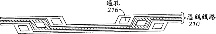
图2A示出的是根据本发明实施例的例示触摸传感器面板200的一部分的侧视图,其中示出了连接迹线204与总线线路210之间的耦合。在图2A中,总线线路210和焊盘218(例如,具有电阻为每方块1欧姆的金属)可以在基板220(例如,厚度为500微米+/-50微米的玻璃)上形成。然后,在总线线路210和焊盘218上可以形成绝缘层214(例如,厚度至少为3微米的有机聚合物),并且通过图案化该绝缘层214来产生通孔216。然后,在绝缘层214上可以形成连接迹线204并使其进入通孔216,以在迹线与总线线路210之间进行连接。另外,在焊盘218上的位置222处还可以局部形成用于形成连接迹线204的同种导电材料,以便保护焊盘。在基板220的背侧上,在基板220上可以形成导电屏蔽层224(例如,厚度为50微米+/-10微米的ITO),以便屏蔽感测线路(图2A中未示出)。然后,通过使用粘合剂(例如,25微米的PSA层),可以将特定厚度(例如,75微米+/-15微米)的抗反射(AR)膜226附加至屏蔽层224。通过使用能形成导电接合的粘合剂228(例如,各向异性导电膜(ACF)),可以将柔性电路212附接至触摸传感器面板200的顶部以及底部。最后,通过使用粘合剂232(例如,厚度为150微米+/-25微米的低酸性压敏粘合剂(PSA)),可以将触摸传感器面板200接合至覆盖材料230(例如,厚度为800至1100微米的玻璃)。FIG. 2A illustrates a side view of a portion of an exemplary
图2B示出的是根据本发明实施例的图2A的例示总线线路210的一部分的顶视图。应该指出的是,在图2B的示例中,在通孔216为总线线路210和连接迹线之间提供连接的点,顶部总线线路的宽度较宽(例如,100微米)。FIG. 2B shows a top view of a portion of the
再次参照图1C的示例,相比于总线线路B7(及其到块体R7C0和R7C1的连接迹线),总线线路B0到块体R0C0和R0C1的连接迹线104在长度上要短很多,因此,总线线路B7的阻抗和电容会比总线线路B0的阻抗和电容大很多。由于这种不平衡性,用于指定触摸量的触摸量度在触摸传感器面板上有可能是不均衡的。因此,在本发明的一些实施例中,耦合至特定总线线路的块体可以交错,以使每条总线线路承受更为均匀的平均阻抗和电容,这样做有助于均衡触摸传感器面板上的触摸量度。Referring again to the example of FIG. 1C , the
图3示出的是根据本发明实施例的例示触摸传感器面板300的一部分,其中包括形成为块体302的驱动线路(或感测线路),并且所述块体302的连接迹线304是交错的。为了清楚起见,图3是以象征性方式而不是按比例绘制的,并且在图3的示例中,总线线路B0耦合至块体R0C0(离B0最近、相邻于列C0的块体)及块体R7C1(离B0最远、相邻于列C1的块体)。总线线路B1耦合至块体R1C0(离B0第二近、相邻于列C0的块体)及块体R6C1(离B0第二远、相邻于列C1的块体)。这种耦合模式对其他总线线路重复进行,这一点可以用总线线路B7耦合至块体R7C0(离B0最远、相邻于列C0的块)及块体R0C1(离B0最近、相邻于列C1的块体)来表明。通过像上文中描述的那样交错耦合至任何特定总线线路的块体,每条总线线路将会承受更均匀的平均阻抗和电容,这样有助于均衡触摸传感器面板上的触摸量度。然而应该理解,对于指定的总线线路来说,借助这种布置,受到激励的块体的位置可能会有很大变化。但是,对所获得的触摸图像的后期处理可以辨别实际触摸位置。3 shows a portion of an exemplary touch sensor panel 300 including drive lines (or sense lines) formed as
另外,交错处理还可增大功率均匀性。在不交错的情况下,一些驱动器可能具有很小的电容负载,而其他驱动器可能具有很大的电容负载。为了确保最大负载能被正确驱动,需将所有驱动器都设计成能够驱动最大电容负载,由此导致对所有驱动器的电流要求增高,甚至是那些驱动负载不大的驱动器。但是,通过交错处理,每个驱动器都可以具有更为适中且大体相等的电容负载,并且只需要将驱动器设计成能够驱动适中的电容负载。In addition, interleaving can also increase power uniformity. Without interleaving, some drivers may have a small capacitive load, while others may have a large capacitive load. To ensure that the largest loads are driven correctly, all drivers need to be designed to drive the largest capacitive loads, resulting in higher current requirements for all drivers, even those driving light loads. However, by interleaving, each driver can have a more moderate and roughly equal capacitive load, and the drivers need only be designed to drive moderate capacitive loads.
图4A示出的是根据本发明实施例的例示触摸传感器面板400,其中包括形成为列406的感测线路(或驱动线路)、形成为块体402的行的驱动线路(或感测线路)以及沿着块体两侧布线(所谓的“双逃逸”配置)的连接迹线404(图中象征性地示为细线)。在图4A的示例中,感测线路(或驱动线路)C0-C3可以形成为列406,且驱动线路(或感测线路)R0-R7可以形成为块体402的行,其中块体的每个行形成单独的驱动线路(或感测线路)。尽管图中显示触摸传感器面板400具有4列8行,但是应当理解,可以使用任何数量的列和行。图4A中的列406和块体402在共面的单个导电材料层中形成。4A shows an exemplary touch sensor panel 400 including sense lines (or drive lines) formed as
为了将特定行中的块体402耦合在一起,同样由导电材料形成的连接迹线404可以沿着块体的交替侧面并以双逃逸配置方式从块体布线至特定的下部总线线路410或上部总线线路414(但是应当理解,在其他实施例中也可以只使用处于顶部或底部的单组总线线路)。由导电材料形成的接地保护装置416可以在连接迹线404与相邻的列406之间形成。下部总线线路410和上部总线线路414以及列406的连接迹线可以沿着边界区域布线,并且可以通过柔性电路从触摸传感器面板400脱离。To couple blocks 402 together in a particular row, connecting
图4B示出的是根据本发明实施例的图4A的例示触摸传感器面板400的一部分的近视图,其中示出了如何可以使用连接迹线404以双逃逸配置方式将块体402布线至下部总线线路410。在图4B的示例中,在双逃逸配置中,连接迹线404-R0-E可以直接布线至下部总线线路410,连接迹线404-R1-E可以沿着块体R0-E的右侧布线,连接迹线404-R2-E可以沿着块体R0-E和R1-E的左侧布线,并且连接迹线404-R3-E可以沿着块体R0-E、R1-E和R2-E(未示出)的右侧布线。FIG. 4B illustrates a close-up view of a portion of the exemplary touch sensor panel 400 of FIG. 4A showing how connecting
在图4B的互电容双逃逸实施例中,每个像素可以用一个列与两个相邻块体之间的互电容来表征(characterized)。例如,R0-C3的像素或传感器可以用块体R0-D与C3之间的互电容418以及块体R0-E与C3之间的互电容420形成。In the mutual capacitance double escape embodiment of Figure 4B, each pixel can be characterized by the mutual capacitance between a column and two adjacent blocks. For example, a pixel or sensor of R0-C3 may be formed with a
如上所述,可选的接地保护装置可以在图4A和图4B中每个列的周围形成,并且还可以在图1A、图1B、图1C和图3中每个列的周围形成。在一个实施例中,所述列的宽度可以是大约1000微米,并且接地保护装置的宽度约为250微米。使用接地保护装置的一个好处是改进了触摸传感器面板的触摸事件检测性能。As described above, optional ground guards may be formed around each column in FIGS. 4A and 4B , and may also be formed around each column in FIGS. 1A , 1B, 1C and 3 . In one embodiment, the columns may be approximately 1000 microns wide and the ground guards may be approximately 250 microns wide. One benefit of using a ground guard is improved touch event detection performance of the touch sensor panel.
图5A和5B示出的是根据本发明实施例的例示接地保护装置500对多边形导电材料区域502产生的效应的顶视图和侧视图。5A and 5B illustrate top and side views of the effect of an exemplary
图5A示出的是不带接地保护装置的示例。当激励信号驱动多边形导电材料区域502或列504时,在多边形区域502与列504之间会出现边缘电场线506。如侧视图所示,在该过程中,一些电场线会暂时离开玻璃盖508。电场线506包括近电场线510,所述近电场线510通常不会离开玻璃盖508,由此不大会受到出现在玻璃盖上或附近的手指的影响。例如,近电场线510可以产生大约2.4pF的杂散电容Csig,但是触摸事件期间的杂散电容变化ΔCsig可能仅为0.05pF,这是一个大约2%的很小变化。电场线506还包括远电场线512,一些远电场线512会暂时离开玻璃盖506并被手指阻挡。与近电场线510相比,远电场线512可以产生约0.6pF的Csig,但在触摸事件期间会经历约0.3pF的杂散电容变化ΔCsig,这是一个约50%的很大变化。这种大的变化代表了更好的信噪比(SNR)以及改进的触摸事件检测。Figure 5A shows an example without a ground protection device. When the excitation signal drives either the polygonal region of
但是,当多边形导电区域502或者列504受到激励时,由于近电场线510和远电场线512全都存在,因此上述示例中产生的总Csig约为3.0pF,并且触摸事件期间的杂散电容的总体变化ΔCsig约为0.35pF,这表明仅有大约10%的变化。为了最大化触摸事件期间杂散电容的百分比变化,较为理想的是将不受触摸事件影响的互电容量(即,近电场线510)减至最小,以及改为尽可能依赖由触摸事件改变的互电容(即,远电场线512)。However, when either the polygonal
图5B示出是带有接地保护装置500的示例。如图5B所示,接地保护装置500可以通过如下方式来减少驱动线路与感测线路之间的不期望的互电容:不允许将近电场线510耦合至感测线路504,而是将大多数近电场线510直接分流至接地,由此主要让远电场线512受到触摸事件的影响。在主要由远电场线512影响互电容值的情况下,如上所述,触摸事件期间的电容变化有可能接近50%,这表明SNR得到了改进。FIG. 5B shows an example with a
图5C和5D示出的是根据本发明实施例的例示接地保护装置500对连接迹线514产生的效应的顶视图和侧视图。图5C示出的是不带接地保护装置的示例。由于连接迹线514可以耦合至多边形导电区域,因此,连接迹线514也会受到激励信号的驱动。如图5C中所示,在不带接地保护装置的情况下,近电场线510会耦合到相邻的感测线路504,从而导致感测线路上发生不期望的电容变化。但是,如图5D所示,如果在适当位置设有接地保护装置500,那么近电场线510会被分流至接地保护装置,而不是耦合到感测线路504,由此减少了感测线路上的不期望的电容变化。5C and 5D illustrate top and side views of the effect of an exemplary
图5E和图5F示出的是根据本发明实施例的例示接地保护装置500对多边形导电区域502产生的效应的顶视图和侧视图,多边形导电区域502通过连接迹线514与感测线路504分离。如图5E中所示,在不带接地保护装置的情况下,近电场线510可以耦合到感测线路504上,从而减少当发生触摸事件时的感测线路上的电容变化百分比。但是,如图5F所示,如果在适当位置设有接地保护装置500,那么近电场线510会被分流至接地保护装置,而不是耦合到感测线路504,由此让大多数远电场线512受触摸事件的影响,从而增大了发生触摸事件时感测线路上的电容百分比变化。5E and 5F illustrate top and side views of the effect of an exemplary
再次参照图1A,先前提到的接地隔离条可以将连接迹线与感测线路之间的杂散电容量Csig减至最小。然而,对于最长的布线迹线来说,仍会有数量级约为6pF的Csig从连接迹线转移到感测线路,由此可能减少动态范围预算并使得校准难以进行。由于从连接迹线到感测线路的杂散电容略微受到触摸事件影响,因此,该杂散电容有可能导致空间交互耦合,其中触摸传感器面板的一个区域内的触摸事件会额外导致杂散电容减小并且在面板的远端区域中出现明显的触摸事件(但这是假的触摸事件)。Referring again to FIG. 1A , the previously mentioned ground spacer bars can minimize the stray capacitance Csig between the connection trace and the sense line. However, for the longest wiring traces, there will still be Csig on the order of 6pF transferred from the connecting trace to the sensing line, thereby potentially reducing the dynamic range budget and making calibration difficult. Since the stray capacitance from the connection trace to the sense line is slightly affected by the touch event, this stray capacitance has the potential to cause spatial interaction coupling where a touch event in one area of the touch sensor panel additionally causes a reduction in the stray capacitance. Small and noticeable touch events in the far area of the panel (but this is a fake touch event).
图6示出的是根据本发明实施例的例示之字形双插式触摸传感器面板600的一部分,它可以进一步减少连接迹线与感测线路之间的杂散电容。在图6的示例中,表示驱动线路(或感测线路)的多边形区域602的形状通常是五边形,并且其取向是交错的,其中位于面板端部附近的一些块体是被切断的五边形区域。感测线路(或驱动线路)604是之字形形状,接地保护装置606则位于感测线路(或驱动线路)与五边形区域602之间。所有连接迹线608都在五边形区域602之间的通道610中布线。在互电容实施例中,每个像素或传感器由五边形区域与相邻感测线路(或驱动线路)604之间形成的电场线616表征。由于连接迹线608并非沿着任何感测线路(或驱动线路)604延伸,而是在五边形区域602之间延伸,因此,连接迹线608与感测线路(或驱动线路)604之间的杂散电容被最小化,并且空间交互耦合也被最小化。先前,连接迹线608与感测线路(或驱动线路)604之间的距离仅为接地保护装置606的宽度,而在图6的实施例中,该距离为接地保护装置的宽度加上五边形区域602的宽度(该宽度沿着五边形形状的长度而有所不同)。FIG. 6 shows a portion of an exemplary zigzag dual plug-in
如图6的示例所示,位于触摸传感器面板末端处的行R14的五边形区域可能被截短。因此,为R14的触摸计算的质心612可能在y方向上偏离其真实位置。另外,为任何两个相邻行的触摸计算的质心将会沿x方向错开(彼此偏移)一个偏移距离。但是,这种失配可以用软件算法来纠正,从而重新映射(re-map)像素并消除失真。As shown in the example of FIG. 6, the pentagonal area of row R14 at the end of the touch sensor panel may be truncated. Therefore, the
尽管在这里主要是依照互电容触摸传感器面板来描述本发明实施例的,但是应当理解,本发明实施例同样适用于自电容触摸传感器面板。在此类实施例中,参考接地平面可以在基板背侧上形成;或者在基板的与多边形区域和感测线路相同的一侧上形成但是通过介电层与多边形区域和感测线路隔开;亦或是在单独基板上形成该平面。在自电容触摸传感器面板中,每个像素或传感器都具有相对于参考接地的自电容,这个自电容会因为手指的存在而改变。Although embodiments of the present invention are primarily described herein in terms of mutual capacitive touch sensor panels, it should be understood that embodiments of the present invention are equally applicable to self capacitive touch sensor panels. In such embodiments, the reference ground plane may be formed on the backside of the substrate; or formed on the same side of the substrate as the polygonal region and the sensing lines but separated from the polygonal region and the sensing lines by a dielectric layer; Alternatively, the plane may be formed on a separate substrate. In a self-capacitance touch sensor panel, each pixel or sensor has a self-capacitance with respect to a reference ground, and this self-capacitance changes due to the presence of a finger.
图7示出的是例示计算系统700,其中可以包括如上所述的本发明的一个或多个实施例。计算系统700可以包括一个或多个面板处理器702和外设704,以及面板子系统706。外设704可以包括但不限于随机存取存储器(RAM)或其他类型的存储器或存储装置,监视计时器等等。面板子系统706可以包括但不限于一个或多个感测通道708,通道扫描逻辑块710以及驱动逻辑块714。通道扫描逻辑块710可以存取RAM 712,自主地从感测通道读取数据,以及提供对感测通道的控制。另外,通道扫描逻辑块710可以控制驱动逻辑块714,以便产生不同频率和相位的激励信号716,激励信号716可以有选择地被施加至触摸传感器面板724的驱动线路。在一些实施例中,面板子系统706、面板处理器702和外设704可以集成在一个单独的专用集成电路(ASIC)中。Illustrated in FIG. 7 is an
触摸传感器面板724可以包括具有多条驱动线路和多条感测线路的电容式感测介质,但是也可使用其他感测介质。在互电容实施例中,驱动线路和感测线路的每个相交点可以代表电容式感测节点,并且可以被视为像素(pixel)726。在将触摸传感器面板724视为捕获触摸“图像”时,这时将每个相交点视为像素将会特别有用。换句话说,在面板子系统706已经确定是否在触摸传感器面板中的每个触摸传感器处检测到触摸事件之后,这时可以将多点触摸面板中发生触摸事件的触摸传感器的图案视为触摸“图像”(例如,触摸面板的手指的图案)。触摸传感器面板724中的每个感测线路都被耦合至面板子系统706内的感测通道708(在这里也被称为事件检测和解调电路)。
计算系统700还可包括主处理器728,用于从面板处理器702接收输出并基于该输出执行动作,这些动作可以包括但不限于:移动光标或指针之类的物体,滚动或平移,调节控制设置,打开文档或文件,查看菜单,做出选择,执行指令,操作耦合至主设备的外设,接听电话,电话呼叫,挂断电话,改变音量或音频设置,存储与电话通信相关联的信息,例如地址、常拨号码、已接来电、未接来电,登陆到计算机或计算机网络、允许经授权的个人访问计算机或计算机网络的限制区域,加载与用户喜爱的计算机桌面布局相关联的用户配置文件,允许访问网页内容,打开特定程序,加密或解码讯息等等。主处理器728还能执行可能并非与面板处理相关联的附加功能,并且可以耦接到程序存储装置732和显示装置730(例如,LED显示器),以便为该装置的用户提供用户界面(UI)。当显示装置730部分或完全位于触摸传感器面板724下方时,这时它可以与触摸传感器面板724一同形成触摸屏718。
应该指出的是,如上所述的一个或多个功能可以由保存在存储器(例如,图7外设704的其中一个)内并由面板处理器702执行的固件实施,或者可以由保存在程序存储装置732内并由主处理器728执行的固件来实施。该固件还可以被存储和/或传输于那些由指令执行系统、设备或装置使用或与之结合使用的任何计算机可读介质内,例如,基于计算机的系统、含有处理器的系统、或是其他那些可以从指令执行系统、设备或装置提取指令并执行指令的系统。在本文的语境中,“计算机可读介质”可以是任何能够包含或存储由指令执行系统、设备或装置使用或与之结合使用的程序的介质。计算机可读介质可以包括但不限于:电子、磁性、光学、电磁、红外或半导体系统、设备或装置、便携式计算机磁碟(磁性)、随机存取存储器(RAM)(磁性)、只读存储器(ROM)(磁性)、可擦可编程只读存储器(EPROM)(磁性)、便携式光学磁碟(例如,CD、CD-R、CD-RW、DVD、DVD-R或DVD-RW)、或快闪存储器(例如,袖珍闪存卡、安全数字卡、USB存储装置、记忆棒)等等。It should be noted that one or more of the functions described above may be implemented by firmware stored in memory (e.g., one of peripherals 704 of FIG. 7 ) and executed by
此外,固件还可以在由指令执行系统、设备或装置使用的或与之结合使用的任何传输介质内传输,例如,基于计算机的系统、含有处理器的系统、或是其他那些可以从指令执行系统、设备或装置提取指令并执行指令的其他系统。在本文的语境中,“传输介质”可以是任何能够传递、传播或传输由指令执行系统、设备或装置使用的或与之结合使用的程序的介质。传输可读介质可以包括但不限于:电子、磁性、光学、电磁或红外有线或无线的传送介质。In addition, firmware may be transmitted over any transmission medium used by or in connection with an instruction execution system, device, or apparatus, such as a computer-based system, a system containing a processor, or other , equipment or other systems that fetch instructions and execute them. In the context of this document, a "transmission medium" may be any medium capable of delivering, propagating, or transporting the program used by or in conjunction with the instruction execution system, device, or device. Transmission-readable media may include, but are not limited to, electronic, magnetic, optical, electromagnetic, or infrared wired or wireless transmission media.
图8A示出的是根据本发明实施例的例示移动电话836,它可以包括触摸传感器面板824和显示装置836,其中该触摸传感器面板具有以如上所述的方式形成的行和列。Figure 8A illustrates an exemplary
图8B示出的是根据本发明实施例的例示数字媒体播放器840,它可以包括触摸传感器面板824和显示装置830,其中该触摸传感器面板具有以如上所述的方式形成的行和列。Figure 8B illustrates an exemplary digital media player 840 that may include a touch sensor panel 824 having rows and columns formed as described above and a
图8A和图8B的移动电话和媒体播放器可以很有利地受益于上述触摸传感器面板,这是因为该触摸传感器面板会使这些装置对触摸更加敏感、更薄且更便宜,而这都是可能对消费者满意度和商业成功产生重大影响的重要消费者因素。The mobile phones and media players of Figures 8A and 8B can advantageously benefit from the touch sensor panel described above because it would make these devices more sensitive to touch, thinner and less expensive, all possible Important consumer factors that have a significant impact on consumer satisfaction and business success.
尽管参照附图对本发明的实施例进行了全面描述,但应当指出的是,各种改变和修改对于本领域技术人员而言都是显而易见的。此类改变和修改将视为包含于附权利要求书所限定的本发明实施例的范围以内。Although the embodiments of the present invention have been fully described with reference to the accompanying drawings, it is to be noted that various changes and modifications will be apparent to those skilled in the art. Such changes and modifications are to be considered within the scope of the embodiments of the present invention as defined in the appended claims.
Claims (12)
Applications Claiming Priority (3)
| Application Number | Priority Date | Filing Date | Title |
|---|---|---|---|
| US12/110,024 US8487898B2 (en) | 2008-04-25 | 2008-04-25 | Ground guard for capacitive sensing |
| US12/110,024 | 2008-04-25 | ||
| PCT/US2009/041465 WO2009132150A1 (en) | 2008-04-25 | 2009-04-22 | Ground guard for capacitive sensing |
Publications (2)
| Publication Number | Publication Date |
|---|---|
| CN102016762A CN102016762A (en) | 2011-04-13 |
| CN102016762B true CN102016762B (en) | 2014-05-07 |
Family
ID=40863427
Family Applications (2)
| Application Number | Title | Priority Date | Filing Date |
|---|---|---|---|
| CN200980114531.0A Expired - Fee Related CN102016762B (en) | 2008-04-25 | 2009-04-22 | Ground guard for capacitive sensing |
| CN2009201524013U Expired - Lifetime CN201499150U (en) | 2008-04-25 | 2009-04-24 | Capacitance type touch sensor panel, performance improving system, mobile phone and media player |
Family Applications After (1)
| Application Number | Title | Priority Date | Filing Date |
|---|---|---|---|
| CN2009201524013U Expired - Lifetime CN201499150U (en) | 2008-04-25 | 2009-04-24 | Capacitance type touch sensor panel, performance improving system, mobile phone and media player |
Country Status (6)
| Country | Link |
|---|---|
| US (1) | US8487898B2 (en) |
| EP (1) | EP2307942B1 (en) |
| JP (2) | JP2011524032A (en) |
| KR (1) | KR101233594B1 (en) |
| CN (2) | CN102016762B (en) |
| WO (1) | WO2009132150A1 (en) |
Families Citing this family (150)
| Publication number | Priority date | Publication date | Assignee | Title |
|---|---|---|---|---|
| US8633915B2 (en) | 2007-10-04 | 2014-01-21 | Apple Inc. | Single-layer touch-sensitive display |
| US20090174676A1 (en) | 2008-01-04 | 2009-07-09 | Apple Inc. | Motion component dominance factors for motion locking of touch sensor data |
| US8576193B2 (en) | 2008-04-25 | 2013-11-05 | Apple Inc. | Brick layout and stackup for a touch screen |
| US8487898B2 (en) | 2008-04-25 | 2013-07-16 | Apple Inc. | Ground guard for capacitive sensing |
| US20100059294A1 (en) * | 2008-09-08 | 2010-03-11 | Apple Inc. | Bandwidth enhancement for a touch sensor panel |
| KR101534109B1 (en) * | 2008-12-23 | 2015-07-07 | 삼성전자주식회사 | Capacitive touch panel and touch system having the same |
| US9261997B2 (en) * | 2009-02-02 | 2016-02-16 | Apple Inc. | Touch regions in diamond configuration |
| US8922521B2 (en) | 2009-02-02 | 2014-12-30 | Apple Inc. | Switching circuitry for touch sensitive display |
| US8593410B2 (en) | 2009-04-10 | 2013-11-26 | Apple Inc. | Touch sensor panel design |
| US8957874B2 (en) | 2009-06-29 | 2015-02-17 | Apple Inc. | Touch sensor panel design |
| US8456443B2 (en) * | 2009-07-24 | 2013-06-04 | Synaptics Incorporated | Single-layer touch sensors |
| KR101073333B1 (en) * | 2009-08-27 | 2011-10-12 | 삼성모바일디스플레이주식회사 | Touch Screen Panel and fabrication method thereof |
| KR101746198B1 (en) * | 2009-09-04 | 2017-06-12 | 가부시키가이샤 한도오따이 에네루기 켄큐쇼 | Display device and electronic device |
| US20110134050A1 (en) * | 2009-12-07 | 2011-06-09 | Harley Jonah A | Fabrication of touch sensor panel using laser ablation |
| KR101148837B1 (en) | 2010-03-03 | 2012-05-29 | (주)멜파스 | Apparatus for sensing touch and method for determining touch input |
| US9146644B2 (en) * | 2010-03-08 | 2015-09-29 | Nuvoton Technology Corporation | Systems and methods for detecting multiple touch points in surface-capacitance type touch panels |
| US8363034B2 (en) * | 2010-04-14 | 2013-01-29 | Panasonic Corporation | Touch panel device |
| TWI403937B (en) * | 2010-06-03 | 2013-08-01 | Au Optronics Corp | Touch display device and touch display substrate thereof |
| JP5625503B2 (en) * | 2010-06-03 | 2014-11-19 | パナソニック株式会社 | Input device |
| WO2011154378A1 (en) | 2010-06-07 | 2011-12-15 | Arcelik Anonim Sirketi | A household appliance comprising capacitive touch sensors |
| KR101706232B1 (en) * | 2010-06-29 | 2017-02-15 | 엘지디스플레이 주식회사 | Touch panel |
| US9652088B2 (en) | 2010-07-30 | 2017-05-16 | Apple Inc. | Fabrication of touch sensor panel using laser ablation |
| US10268320B2 (en) | 2010-08-06 | 2019-04-23 | Apple Inc. | Method for disambiguating multiple touches on a projection-scan touch sensor panel |
| KR101447738B1 (en) | 2011-05-26 | 2014-10-06 | 엘지이노텍 주식회사 | Touch window |
| EP2538313B1 (en) * | 2011-06-20 | 2015-05-20 | Melfas, Inc. | Touch sensor panel |
| CN102985835B (en) | 2011-07-15 | 2018-04-13 | 赛普拉斯半导体公司 | Capacitance sensing circuit, method and system with ground connection insertion electrode |
| CN202795311U (en) * | 2011-07-26 | 2013-03-13 | 比亚迪股份有限公司 | Touch control device and portable electronic device |
| US8903679B2 (en) | 2011-09-23 | 2014-12-02 | Cypress Semiconductor Corporation | Accuracy in a capacitive sense array |
| US9612265B1 (en) * | 2011-09-23 | 2017-04-04 | Cypress Semiconductor Corporation | Methods and apparatus to detect a conductive object |
| US9632629B2 (en) | 2011-09-29 | 2017-04-25 | Parade Technologies, Ltd. | Sensor patterns with reduced noise coupling |
| KR20130037001A (en) * | 2011-10-05 | 2013-04-15 | 삼성전자주식회사 | User terminal and touch panel thereof |
| CN103064547B (en) * | 2011-10-21 | 2016-03-16 | 群康科技(深圳)有限公司 | Touch system and matching method thereof |
| US10082889B2 (en) * | 2011-10-28 | 2018-09-25 | Atmel Corporation | Multi-electrode active stylus tip |
| US9634660B2 (en) * | 2011-12-20 | 2017-04-25 | Atmel Corporation | Touch sensor with reduced anti-touch effects |
| CN103197813A (en) * | 2012-01-05 | 2013-07-10 | 宏达国际电子股份有限公司 | Touch panel |
| TWI457813B (en) | 2012-01-08 | 2014-10-21 | Htc Corp | Touch panel |
| JP6052914B2 (en) * | 2012-01-12 | 2016-12-27 | シナプティクス インコーポレイテッド | Single-layer capacitive imaging sensor |
| US9329723B2 (en) | 2012-04-16 | 2016-05-03 | Apple Inc. | Reconstruction of original touch image from differential touch image |
| CN102662551A (en) * | 2012-04-17 | 2012-09-12 | 苏州合美硕触控技术有限公司 | Capacitive touch screen |
| US9134396B2 (en) | 2012-04-17 | 2015-09-15 | Synaptics Incorporated | Reducing bending effects in touch sensor devices |
| JP5718282B2 (en) * | 2012-05-31 | 2015-05-13 | 株式会社東海理化電機製作所 | Capacitance detection device |
| US20130321324A1 (en) * | 2012-06-01 | 2013-12-05 | Touch Turns Llc | System for reducing finger-coupled noise in capacitive touch sensors |
| KR101471349B1 (en) * | 2012-06-15 | 2014-12-11 | 주식회사 실리콘웍스 | Touch panel |
| TW201403767A (en) * | 2012-07-10 | 2014-01-16 | Wintek Corp | Touch panel |
| CN103576998B (en) * | 2012-07-20 | 2017-07-28 | 上海思立微电子科技有限公司 | Capacitive touch screen and single layer cloth line electrode array |
| KR101966861B1 (en) | 2012-07-23 | 2019-04-09 | 삼성디스플레이 주식회사 | Touch screen panel, touch sensing apparatus having the same and driving method thereof |
| US10078404B2 (en) | 2012-07-23 | 2018-09-18 | Samsung Display Co., Ltd. | Touch screen panel and touch sensing apparatus having the same |
| CN103577001A (en) * | 2012-07-27 | 2014-02-12 | 奕力科技股份有限公司 | Single-layer capacitive touch panel device |
| CN102830878A (en) * | 2012-08-17 | 2012-12-19 | 杭州安费诺飞凤通信部品有限公司 | Outgoing line via overlap structure of capacitive touch screen and production method of outgoing line via overlap structure |
| KR101934310B1 (en) | 2012-08-24 | 2019-01-03 | 삼성디스플레이 주식회사 | touch display apparatus sensing touch force |
| TWI548908B (en) | 2012-08-31 | 2016-09-11 | 群創光電股份有限公司 | Touch display device |
| CN103677386B (en) * | 2012-08-31 | 2017-06-20 | 群康科技(深圳)有限公司 | Electrically-conductive backing plate and touch control display apparatus |
| US20140062952A1 (en) | 2012-09-05 | 2014-03-06 | Cypress Semiconductor Corporation | Reducing common mode noise in touch applications |
| KR101474064B1 (en) * | 2012-09-11 | 2014-12-17 | 엘지디스플레이 주식회사 | Touch screen panel for display device |
| KR101463051B1 (en) * | 2012-09-26 | 2014-11-18 | 주식회사 지니틱스 | Conductor pattern, touch panel module, and electric device |
| KR101463052B1 (en) * | 2012-09-26 | 2014-11-18 | 주식회사 지니틱스 | Conductor pattern, touch panel module, and electric device |
| CN102931967B (en) * | 2012-11-09 | 2015-03-11 | 烟台正海科技有限公司 | Key wiring for capacitive touch screen |
| KR101628724B1 (en) * | 2012-11-13 | 2016-06-09 | 엘지디스플레이 주식회사 | Display device with integrated touch screen |
| CN103116427B (en) * | 2012-12-10 | 2016-05-18 | 文山嘉鑫科技有限公司 | Bridging lead-in wire sensor and the moulding process thereof of individual layer multi-point touch screen |
| KR101533971B1 (en) * | 2012-12-13 | 2015-07-06 | 주식회사 지니틱스 | Touch electrode pattern, touch panel, and touch input device having the same |
| CN103105991B (en) * | 2013-01-25 | 2016-04-06 | 深圳市汇顶科技股份有限公司 | Individual layer capacitive touch screen and touch control terminal |
| US9217678B2 (en) * | 2013-02-06 | 2015-12-22 | Nanchang O-Film Tech Co., Ltd. | Touch sensor panel with conductive wires and color traces |
| US9618981B2 (en) * | 2013-02-13 | 2017-04-11 | Synaptics Incorporated | Guarding and shielding routing traces in proximity sensors |
| US9110552B2 (en) | 2013-03-11 | 2015-08-18 | Cypress Semiconductor Corporation | Eliminating common mode noise in otuch applications |
| KR102085727B1 (en) * | 2013-03-12 | 2020-03-09 | 주식회사 실리콘웍스 | Touch panel |
| US9195354B2 (en) | 2013-03-12 | 2015-11-24 | Synaptics Incorporated | Device and method for localized force and proximity sensing |
| KR102044476B1 (en) * | 2013-05-02 | 2019-11-13 | 삼성전자주식회사 | Touch screen panel, touch senssing controller and touch sensing system comprising the same |
| DE102013104644B4 (en) * | 2013-05-06 | 2020-06-04 | Polylc Gmbh & Co. Kg | Layer electrode for touch screens |
| KR101448094B1 (en) * | 2013-05-15 | 2014-10-13 | (주)멜파스 | Touch sensing apparatus using single layer pattern and method for manufacturing the same |
| TW201445621A (en) | 2013-05-24 | 2014-12-01 | Wintek Corp | Touch-sensing electrode structure and touch-sensitive device |
| TW201447703A (en) * | 2013-06-07 | 2014-12-16 | Wintek Corp | Touch apparatus and driving method thereof |
| TW201501002A (en) * | 2013-06-18 | 2015-01-01 | Novatek Microelectronics Corp | Single-layer capacitive touch screen |
| US9201468B2 (en) | 2013-06-28 | 2015-12-01 | Synaptics Incorporated | Device and method for proximity sensing with force imaging |
| US9552089B2 (en) | 2013-08-07 | 2017-01-24 | Synaptics Incorporated | Capacitive sensing using a matrix electrode pattern |
| US9886141B2 (en) | 2013-08-16 | 2018-02-06 | Apple Inc. | Mutual and self capacitance touch measurements in touch panel |
| KR101502910B1 (en) * | 2013-08-30 | 2015-03-16 | 크루셜텍 (주) | Touch detecting apparatuse for improving visualbility and touch detecting |
| US8872526B1 (en) | 2013-09-10 | 2014-10-28 | Cypress Semiconductor Corporation | Interleaving sense elements of a capacitive-sense array |
| US9495050B1 (en) * | 2013-09-10 | 2016-11-15 | Monterey Research, Llc | Sensor pattern with signal-spreading electrodes |
| KR102081318B1 (en) * | 2013-09-23 | 2020-04-14 | 엘지디스플레이 주식회사 | Touch sensor integrated type liquid crystal display device |
| US10042489B2 (en) | 2013-09-30 | 2018-08-07 | Synaptics Incorporated | Matrix sensor for image touch sensing |
| US9298325B2 (en) | 2013-09-30 | 2016-03-29 | Synaptics Incorporated | Processing system for a capacitive sensing device |
| US20150091842A1 (en) | 2013-09-30 | 2015-04-02 | Synaptics Incorporated | Matrix sensor for image touch sensing |
| US9459367B2 (en) | 2013-10-02 | 2016-10-04 | Synaptics Incorporated | Capacitive sensor driving technique that enables hybrid sensing or equalization |
| KR102140791B1 (en) * | 2013-10-11 | 2020-08-03 | 삼성전자주식회사 | Touch Controller, Electronic Device and Display Device including Touch Controller, and Method for Touch Sensing |
| US9274662B2 (en) | 2013-10-18 | 2016-03-01 | Synaptics Incorporated | Sensor matrix pad for performing multiple capacitive sensing techniques |
| KR102092547B1 (en) * | 2013-10-22 | 2020-03-24 | 엘지디스플레이 주식회사 | Touch panel |
| US9081457B2 (en) | 2013-10-30 | 2015-07-14 | Synaptics Incorporated | Single-layer muti-touch capacitive imaging sensor |
| GB2521835A (en) | 2014-01-02 | 2015-07-08 | Nokia Technologies Oy | Electromagnetic shielding |
| US9465471B2 (en) * | 2014-01-24 | 2016-10-11 | Innolux Corporation | Transparent electrode layer, touch panel and electronic device |
| KR102183655B1 (en) | 2014-01-28 | 2020-11-27 | 삼성디스플레이 주식회사 | Display apparatus |
| US9798429B2 (en) | 2014-02-28 | 2017-10-24 | Synaptics Incorporated | Guard electrodes in a sensing stack |
| CN103853411A (en) * | 2014-03-11 | 2014-06-11 | 泰凌微电子(上海)有限公司 | Induction system |
| KR102271114B1 (en) * | 2014-03-28 | 2021-06-30 | 삼성디스플레이 주식회사 | Touch sensing panel |
| US10133421B2 (en) | 2014-04-02 | 2018-11-20 | Synaptics Incorporated | Display stackups for matrix sensor |
| US9927832B2 (en) | 2014-04-25 | 2018-03-27 | Synaptics Incorporated | Input device having a reduced border region |
| KR102342846B1 (en) | 2014-04-28 | 2021-12-27 | 삼성디스플레이 주식회사 | Flexible display device |
| US9690397B2 (en) | 2014-05-20 | 2017-06-27 | Synaptics Incorporated | System and method for detecting an active pen with a matrix sensor |
| WO2015178304A1 (en) * | 2014-05-21 | 2015-11-26 | シャープ株式会社 | Conductive sheet, touch panel device, and display device |
| WO2015180315A1 (en) * | 2014-05-30 | 2015-12-03 | 京东方科技集团股份有限公司 | Capacitive touch structure, embedded touchscreen, display device and scanning method therefor |
| US9841850B2 (en) | 2014-06-16 | 2017-12-12 | Synaptics Incorporated | Device and method for proximity sensing with force imaging |
| US10289251B2 (en) | 2014-06-27 | 2019-05-14 | Apple Inc. | Reducing floating ground effects in pixelated self-capacitance touch screens |
| US9411458B2 (en) | 2014-06-30 | 2016-08-09 | Synaptics Incorporated | System and method for determining input object information from proximity and force measurements |
| TWI543054B (en) * | 2014-07-09 | 2016-07-21 | 晨星半導體股份有限公司 | Sensing electrode and sensing capacitance estimation method and apparatus |
| US9280251B2 (en) | 2014-07-11 | 2016-03-08 | Apple Inc. | Funneled touch sensor routing |
| KR101748568B1 (en) * | 2014-07-16 | 2017-06-21 | (주)멜파스 | Touch panel using single layer pattern and touch sensing apparatus including the touch panel |
| KR102255163B1 (en) | 2014-08-18 | 2021-05-25 | 삼성디스플레이 주식회사 | Touch sensing device |
| US9880655B2 (en) | 2014-09-02 | 2018-01-30 | Apple Inc. | Method of disambiguating water from a finger touch on a touch sensor panel |
| US9632638B2 (en) * | 2014-09-10 | 2017-04-25 | Synaptics Incorporated | Device and method for force and proximity sensing employing an intermediate shield electrode layer |
| US10185427B2 (en) | 2014-09-11 | 2019-01-22 | Synaptics Incorporated | Device and method for localized force sensing |
| EP3175330B1 (en) | 2014-09-22 | 2022-04-20 | Apple Inc. | Ungrounded user signal compensation for pixelated self-capacitance touch sensor panel |
| US10712867B2 (en) | 2014-10-27 | 2020-07-14 | Apple Inc. | Pixelated self-capacitance water rejection |
| US10175827B2 (en) | 2014-12-23 | 2019-01-08 | Synaptics Incorporated | Detecting an active pen using a capacitive sensing device |
| US10990148B2 (en) | 2015-01-05 | 2021-04-27 | Synaptics Incorporated | Central receiver for performing capacitive sensing |
| AU2016215616B2 (en) | 2015-02-02 | 2018-12-06 | Apple Inc. | Flexible self-capacitance and mutual capacitance touch sensing system architecture |
| KR102381121B1 (en) | 2015-02-02 | 2022-04-01 | 삼성디스플레이 주식회사 | Touch panel and display apparatus having the same |
| US10296147B2 (en) | 2015-02-02 | 2019-05-21 | Samsung Display Co., Ltd. | Touch screen and display device including the same |
| JP2018505486A (en) * | 2015-02-06 | 2018-02-22 | シェンジェン ロイオル テクノロジーズ カンパニー リミテッドShenzhen Royole Technologies Co., Ltd. | Capacitive touch screen and manufacturing method thereof |
| WO2016131963A1 (en) * | 2015-02-19 | 2016-08-25 | T+Ink Gmbh | Self-grounding capacitive information carrier and its use |
| US10488992B2 (en) | 2015-03-10 | 2019-11-26 | Apple Inc. | Multi-chip touch architecture for scalability |
| CN104699354B (en) | 2015-04-01 | 2017-12-22 | 上海天马微电子有限公司 | Touch panel, driving method thereof and touch display device |
| US9939972B2 (en) * | 2015-04-06 | 2018-04-10 | Synaptics Incorporated | Matrix sensor with via routing |
| CN104793386B (en) | 2015-05-08 | 2018-08-24 | 厦门天马微电子有限公司 | Touch array substrate, liquid crystal display panel and liquid crystal display device |
| US10095948B2 (en) | 2015-06-30 | 2018-10-09 | Synaptics Incorporated | Modulation scheme for fingerprint sensing |
| US9671915B2 (en) | 2015-06-30 | 2017-06-06 | Synaptics Incorporated | Avoidance of bending effects in a touch sensor device |
| US9715304B2 (en) | 2015-06-30 | 2017-07-25 | Synaptics Incorporated | Regular via pattern for sensor-based input device |
| US9720541B2 (en) | 2015-06-30 | 2017-08-01 | Synaptics Incorporated | Arrangement of sensor pads and display driver pads for input device |
| CN104965628B (en) * | 2015-07-17 | 2018-03-23 | 合肥京东方光电科技有限公司 | Capacitance type touch control substrate and touching display screen |
| KR102025283B1 (en) * | 2015-08-25 | 2019-09-26 | 주식회사 엘지화학 | Single plate touch sensor advanced touch sensitivity |
| CN205028263U (en) | 2015-09-07 | 2016-02-10 | 辛纳普蒂克斯公司 | Capacitance sensor |
| US20170075473A1 (en) * | 2015-09-15 | 2017-03-16 | Hyundai Motor Company | Touch input device and method for manufacturing the same |
| US10310667B2 (en) | 2015-09-21 | 2019-06-04 | Apple Inc. | Multi-bar capacitive sense electrode |
| US10534481B2 (en) | 2015-09-30 | 2020-01-14 | Apple Inc. | High aspect ratio capacitive sensor panel |
| US10037112B2 (en) | 2015-09-30 | 2018-07-31 | Synaptics Incorporated | Sensing an active device'S transmission using timing interleaved with display updates |
| US10365773B2 (en) | 2015-09-30 | 2019-07-30 | Apple Inc. | Flexible scan plan using coarse mutual capacitance and fully-guarded measurements |
| KR102408442B1 (en) | 2015-10-20 | 2022-06-14 | 삼성디스플레이 주식회사 | Touch sensor and liquid crystal display including the same |
| JP2017084212A (en) * | 2015-10-30 | 2017-05-18 | 株式会社ジャパンディスプレイ | Sensor and display device provided with sensor |
| KR102402256B1 (en) | 2015-11-04 | 2022-05-27 | 삼성디스플레이 주식회사 | Display device |
| US10067587B2 (en) | 2015-12-29 | 2018-09-04 | Synaptics Incorporated | Routing conductors in an integrated display device and sensing device |
| CN106933400B (en) | 2015-12-31 | 2021-10-29 | 辛纳普蒂克斯公司 | Single-layer sensor pattern and sensing method |
| US20170277348A1 (en) * | 2016-03-25 | 2017-09-28 | Uico, Llc | Capacitive touch sensing system with improved guarding scheme and devices employing same |
| US10452212B2 (en) * | 2016-04-12 | 2019-10-22 | Apple Inc. | Mitigating active stylus/touch cross-coupling |
| AU2017208277B2 (en) | 2016-09-06 | 2018-12-20 | Apple Inc. | Back of cover touch sensors |
| US10261622B2 (en) | 2016-10-10 | 2019-04-16 | Microsoft Technology Licensing, Llc | Ground reference floating in a touch-sensitive display |
| US10386965B2 (en) | 2017-04-20 | 2019-08-20 | Apple Inc. | Finger tracking in wet environment |
| KR102563311B1 (en) * | 2018-11-16 | 2023-08-04 | 삼성전자주식회사 | Cooking apparatus and controlling method there of |
| KR102698410B1 (en) * | 2019-01-24 | 2024-08-23 | 삼성디스플레이 주식회사 | Touch sensing unit and display device including the same |
| KR102315144B1 (en) | 2019-04-02 | 2021-10-21 | 주식회사 하이딥 | Touch input device |
| CN110389686B (en) * | 2019-07-25 | 2023-09-08 | 京东方科技集团股份有限公司 | A touch device, a display device and a method for preparing the touch device |
| KR102637829B1 (en) * | 2019-10-28 | 2024-02-19 | 엘지디스플레이 주식회사 | Touch display device |
| US11662867B1 (en) | 2020-05-30 | 2023-05-30 | Apple Inc. | Hover detection on a touch sensor panel |
Family Cites Families (82)
| Publication number | Priority date | Publication date | Assignee | Title |
|---|---|---|---|---|
| US4087625A (en) | 1976-12-29 | 1978-05-02 | International Business Machines Corporation | Capacitive two dimensional tablet with single conductive layer |
| US4304976A (en) | 1978-03-16 | 1981-12-08 | Texas Instruments Incorporated | Capacitive touch switch panel |
| IT1194351B (en) | 1983-07-28 | 1988-09-22 | Snam Progetti | PROCEDURE FOR THE RECOVERY OF BUTENE-1 DEGREE POLYMERIZATION |
| US4659874A (en) * | 1985-09-23 | 1987-04-21 | Sanders Associates, Inc. | X-Y position sensor |
| US5459463A (en) | 1990-05-25 | 1995-10-17 | Sextant Avionique | Device for locating an object situated close to a detection area and a transparent keyboard using said device |
| GB2245708A (en) | 1990-06-29 | 1992-01-08 | Philips Electronic Associated | Touch sensor array systems |
| US5223796A (en) * | 1991-05-28 | 1993-06-29 | Axiomatics Corporation | Apparatus and methods for measuring the dielectric and geometric properties of materials |
| US5483261A (en) * | 1992-02-14 | 1996-01-09 | Itu Research, Inc. | Graphical input controller and method with rear screen image detection |
| US5880411A (en) * | 1992-06-08 | 1999-03-09 | Synaptics, Incorporated | Object position detector with edge motion feature and gesture recognition |
| US5488204A (en) * | 1992-06-08 | 1996-01-30 | Synaptics, Incorporated | Paintbrush stylus for capacitive touch sensor pad |
| US5317919A (en) | 1992-06-16 | 1994-06-07 | Teledyne Industries, Inc. | A precision capacitor sensor |
| US5825352A (en) * | 1996-01-04 | 1998-10-20 | Logitech, Inc. | Multiple fingers contact sensing method for emulating mouse buttons and mouse operations on a touch sensor pad |
| US5835079A (en) * | 1996-06-13 | 1998-11-10 | International Business Machines Corporation | Virtual pointing device for touchscreens |
| GB2321108A (en) | 1997-01-08 | 1998-07-15 | David Alan Woodfield | Input device for inputting positional information |
| US6310610B1 (en) * | 1997-12-04 | 2001-10-30 | Nortel Networks Limited | Intelligent touch display |
| US8479122B2 (en) * | 2004-07-30 | 2013-07-02 | Apple Inc. | Gestures for touch sensitive input devices |
| KR100595922B1 (en) * | 1998-01-26 | 2006-07-05 | 웨인 웨스터만 | Method and apparatus for integrating manual input |
| US7663607B2 (en) * | 2004-05-06 | 2010-02-16 | Apple Inc. | Multipoint touchscreen |
| US6188391B1 (en) * | 1998-07-09 | 2001-02-13 | Synaptics, Inc. | Two-layer capacitive touchpad and method of making same |
| JP4542637B2 (en) | 1998-11-25 | 2010-09-15 | セイコーエプソン株式会社 | Portable information device and information storage medium |
| US6297811B1 (en) | 1999-06-02 | 2001-10-02 | Elo Touchsystems, Inc. | Projective capacitive touchscreen |
| GB0014074D0 (en) | 2000-06-10 | 2000-08-02 | Koninkl Philips Electronics Nv | Active matrix array devices |
| JP3800984B2 (en) | 2001-05-21 | 2006-07-26 | ソニー株式会社 | User input device |
| JP2003066417A (en) | 2001-08-22 | 2003-03-05 | Sharp Corp | Touch sensor integrated display |
| JP2003173237A (en) * | 2001-09-28 | 2003-06-20 | Ricoh Co Ltd | Information input / output system, program and storage medium |
| US6690387B2 (en) * | 2001-12-28 | 2004-02-10 | Koninklijke Philips Electronics N.V. | Touch-screen image scrolling system and method |
| US11275405B2 (en) * | 2005-03-04 | 2022-03-15 | Apple Inc. | Multi-functional hand-held device |
| CA2490490A1 (en) * | 2002-07-03 | 2004-01-15 | Quelis Id Systems Inc. | Wire positioning and mechanical attachment for a radio-frequency identification device |
| US20040017362A1 (en) * | 2002-07-23 | 2004-01-29 | Mulligan Roger C. | Thin face capacitive touch screen |
| WO2004013833A2 (en) | 2002-08-02 | 2004-02-12 | Cirque Corporation | Single-layer touchpad having touch zones |
| US20040090429A1 (en) | 2002-11-12 | 2004-05-13 | Geaghan Bernard O. | Touch sensor and method of making |
| US7129935B2 (en) * | 2003-06-02 | 2006-10-31 | Synaptics Incorporated | Sensor patterns for a capacitive sensing apparatus |
| CA2529688A1 (en) | 2003-06-20 | 2004-12-29 | Cirque Corporation | Single-layer touchpad and methods of use |
| JP4496738B2 (en) | 2003-09-04 | 2010-07-07 | ソニー株式会社 | Image display device |
| US20050073507A1 (en) | 2003-10-06 | 2005-04-07 | Richter Paul J. | Touch input sensing device |
| US8068186B2 (en) | 2003-10-15 | 2011-11-29 | 3M Innovative Properties Company | Patterned conductor touch screen having improved optics |
| US7307624B2 (en) * | 2003-12-30 | 2007-12-11 | 3M Innovative Properties Company | Touch sensor with linearized response |
| US7382139B2 (en) * | 2004-06-03 | 2008-06-03 | Synaptics Incorporated | One layer capacitive sensing apparatus having varying width sensing elements |
| US7737953B2 (en) | 2004-08-19 | 2010-06-15 | Synaptics Incorporated | Capacitive sensing apparatus having varying depth sensing elements |
| US7138620B2 (en) * | 2004-10-29 | 2006-11-21 | Silicon Light Machines Corporation | Two-dimensional motion sensor |
| KR20060062164A (en) * | 2004-12-03 | 2006-06-12 | 삼성전자주식회사 | Display device with built-in light sensor |
| KR100651559B1 (en) * | 2004-12-30 | 2006-11-29 | 삼성전기주식회사 | High frequency signal transmission line with improved noise characteristics |
| US20060227114A1 (en) | 2005-03-30 | 2006-10-12 | Geaghan Bernard O | Touch location determination with error correction for sensor movement |
| US7567240B2 (en) | 2005-05-31 | 2009-07-28 | 3M Innovative Properties Company | Detection of and compensation for stray capacitance in capacitive touch sensors |
| US7138686B1 (en) * | 2005-05-31 | 2006-11-21 | Freescale Semiconductor, Inc. | Integrated circuit with improved signal noise isolation and method for improving signal noise isolation |
| GB2428306B (en) | 2005-07-08 | 2007-09-26 | Harald Philipp | Two-dimensional capacitive position sensor |
| GB0519170D0 (en) * | 2005-09-20 | 2005-10-26 | Philipp Harald | Capacitive touch sensor |
| JP2007086990A (en) | 2005-09-21 | 2007-04-05 | Smk Corp | Touch panel |
| US7864160B2 (en) * | 2005-10-05 | 2011-01-04 | 3M Innovative Properties Company | Interleaved electrodes for touch sensing |
| US8549442B2 (en) * | 2005-12-12 | 2013-10-01 | Sony Computer Entertainment Inc. | Voice and video control of interactive electronically simulated environment |
| US8144125B2 (en) * | 2006-03-30 | 2012-03-27 | Cypress Semiconductor Corporation | Apparatus and method for reducing average scan rate to detect a conductive object on a sensing device |
| US7538760B2 (en) | 2006-03-30 | 2009-05-26 | Apple Inc. | Force imaging input device and system |
| DE202007005237U1 (en) | 2006-04-25 | 2007-07-05 | Philipp, Harald, Southampton | Touch-sensitive position sensor for use in control panel, has bus bars arranged at distance to substrate, and detection region with units that are arranged at distance by non-conductive openings such that current flows into region |
| TW200805128A (en) | 2006-05-05 | 2008-01-16 | Harald Philipp | Touch screen element |
| JP4654211B2 (en) | 2006-05-09 | 2011-03-16 | アップル インコーポレイテッド | Force / position sensing display |
| US8619054B2 (en) | 2006-05-31 | 2013-12-31 | Atmel Corporation | Two dimensional position sensor |
| KR101295943B1 (en) | 2006-06-09 | 2013-08-13 | 애플 인크. | Touch screen liquid crystal display |
| GB0613983D0 (en) | 2006-07-13 | 2006-08-23 | Synaptics Uk Ltd | Digitising System |
| US20080074398A1 (en) * | 2006-09-26 | 2008-03-27 | David Gordon Wright | Single-layer capacitive sensing device |
| US8026903B2 (en) | 2007-01-03 | 2011-09-27 | Apple Inc. | Double-sided touch sensitive panel and flex circuit bonding |
| KR100885730B1 (en) | 2007-03-05 | 2009-02-26 | (주)멜파스 | Touch location sensing pannel having a simple layer structure |
| TW200842681A (en) | 2007-04-27 | 2008-11-01 | Tpk Touch Solutions Inc | Touch pattern structure of a capacitive touch panel |
| CN101681223A (en) | 2007-05-07 | 2010-03-24 | 爱特梅尔公司 | Two-dimensional position sensor |
| TW200844827A (en) | 2007-05-11 | 2008-11-16 | Sense Pad Tech Co Ltd | Transparent touch panel device |
| US20080309633A1 (en) | 2007-06-13 | 2008-12-18 | Apple Inc. | Touch-sensitive display |
| JP4506785B2 (en) | 2007-06-14 | 2010-07-21 | エプソンイメージングデバイス株式会社 | Capacitive input device |
| TW200901014A (en) | 2007-06-28 | 2009-01-01 | Sense Pad Tech Co Ltd | Touch panel device |
| KR100902051B1 (en) | 2007-07-12 | 2009-06-15 | 주식회사 하이닉스반도체 | Error checking code generator and method |
| US20090054107A1 (en) * | 2007-08-20 | 2009-02-26 | Synaptics Incorporated | Handheld communication device and method for conference call initiation |
| US8633915B2 (en) | 2007-10-04 | 2014-01-21 | Apple Inc. | Single-layer touch-sensitive display |
| TWM344544U (en) | 2007-12-25 | 2008-11-11 | Cando Corp | Sensory structure of touch panel |
| JP5094376B2 (en) | 2007-12-28 | 2012-12-12 | 株式会社ワコム | Position detection device |
| TWM344522U (en) | 2008-03-18 | 2008-11-11 | Cando Corp | Sensory structure of capacitive touch panel and capacitive touch panel having the same |
| TWI361996B (en) | 2008-03-21 | 2012-04-11 | Elan Microelectronics Corp | Touch panel device |
| TWI389020B (en) | 2008-03-25 | 2013-03-11 | Elan Microelectronics | Touch panel device |
| US8487898B2 (en) * | 2008-04-25 | 2013-07-16 | Apple Inc. | Ground guard for capacitive sensing |
| US8576193B2 (en) | 2008-04-25 | 2013-11-05 | Apple Inc. | Brick layout and stackup for a touch screen |
| US20090309850A1 (en) | 2008-06-16 | 2009-12-17 | Kai-Ti Yang | Capacitive touch panel |
| JP4720857B2 (en) | 2008-06-18 | 2011-07-13 | ソニー株式会社 | Capacitance type input device and display device with input function |
| US8319747B2 (en) | 2008-12-11 | 2012-11-27 | Apple Inc. | Single layer touch panel with segmented drive and sense electrodes |
| WO2010117882A2 (en) | 2009-04-10 | 2010-10-14 | Apple Inc. | Improved touch sensor panel design |
| US8593410B2 (en) | 2009-04-10 | 2013-11-26 | Apple Inc. | Touch sensor panel design |
-
2008
- 2008-04-25 US US12/110,024 patent/US8487898B2/en not_active Expired - Fee Related
-
2009
- 2009-04-22 EP EP09735774.3A patent/EP2307942B1/en not_active Not-in-force
- 2009-04-22 WO PCT/US2009/041465 patent/WO2009132150A1/en not_active Ceased
- 2009-04-22 KR KR1020107026318A patent/KR101233594B1/en not_active Expired - Fee Related
- 2009-04-22 JP JP2011506442A patent/JP2011524032A/en active Pending
- 2009-04-22 CN CN200980114531.0A patent/CN102016762B/en not_active Expired - Fee Related
- 2009-04-24 CN CN2009201524013U patent/CN201499150U/en not_active Expired - Lifetime
-
2014
- 2014-02-28 JP JP2014039236A patent/JP5958775B2/en not_active Expired - Fee Related
Also Published As
| Publication number | Publication date |
|---|---|
| WO2009132150A1 (en) | 2009-10-29 |
| JP2014139812A (en) | 2014-07-31 |
| KR101233594B1 (en) | 2013-02-14 |
| US8487898B2 (en) | 2013-07-16 |
| KR20110007220A (en) | 2011-01-21 |
| EP2307942B1 (en) | 2018-08-29 |
| US20090267916A1 (en) | 2009-10-29 |
| CN102016762A (en) | 2011-04-13 |
| JP5958775B2 (en) | 2016-08-02 |
| CN201499150U (en) | 2010-06-02 |
| EP2307942A1 (en) | 2011-04-13 |
| JP2011524032A (en) | 2011-08-25 |
Similar Documents
| Publication | Publication Date | Title |
|---|---|---|
| CN102016762B (en) | Ground guard for capacitive sensing | |
| CN101566895B (en) | Brick layout and stackup for touch screen | |
| CN102057349B (en) | High Resistivity Metal Fan-Out | |
| US9582131B2 (en) | Touch sensor panel design | |
| CN102822776B (en) | The impact of stray capacitance in balanced touch-screen | |
| NL2001672C2 (en) | Touch sensitive display. | |
| TWI484398B (en) | Touch sensor panel, method for forming the same, a mobile telephone including the same, and a digital media player including the same | |
| US8593410B2 (en) | Touch sensor panel design | |
| US9304641B2 (en) | Multiple bridges single sided touch sensor | |
| WO2010117882A2 (en) | Improved touch sensor panel design | |
| HK1156413B (en) | Ground guard for capacitive sensing | |
| HK1156413A (en) | Ground guard for capacitive sensing | |
| AU2012205167B2 (en) | High resistivity metal fan out |
Legal Events
| Date | Code | Title | Description |
|---|---|---|---|
| C06 | Publication | ||
| PB01 | Publication | ||
| C10 | Entry into substantive examination | ||
| SE01 | Entry into force of request for substantive examination | ||
| C14 | Grant of patent or utility model | ||
| GR01 | Patent grant | ||
| CF01 | Termination of patent right due to non-payment of annual fee |
Granted publication date: 20140507 Termination date: 20210422 |
|
| CF01 | Termination of patent right due to non-payment of annual fee |