CN102015921A - Method and composition for screen printing of conductive features - Google Patents
Method and composition for screen printing of conductive features Download PDFInfo
- Publication number
- CN102015921A CN102015921A CN2009801148126A CN200980114812A CN102015921A CN 102015921 A CN102015921 A CN 102015921A CN 2009801148126 A CN2009801148126 A CN 2009801148126A CN 200980114812 A CN200980114812 A CN 200980114812A CN 102015921 A CN102015921 A CN 102015921A
- Authority
- CN
- China
- Prior art keywords
- conductive
- nanostructures
- anisotropic
- coating composition
- substrate
- Prior art date
- Legal status (The legal status is an assumption and is not a legal conclusion. Google has not performed a legal analysis and makes no representation as to the accuracy of the status listed.)
- Granted
Links
Images


Classifications
-
- C—CHEMISTRY; METALLURGY
- C09—DYES; PAINTS; POLISHES; NATURAL RESINS; ADHESIVES; COMPOSITIONS NOT OTHERWISE PROVIDED FOR; APPLICATIONS OF MATERIALS NOT OTHERWISE PROVIDED FOR
- C09D—COATING COMPOSITIONS, e.g. PAINTS, VARNISHES OR LACQUERS; FILLING PASTES; CHEMICAL PAINT OR INK REMOVERS; INKS; CORRECTING FLUIDS; WOODSTAINS; PASTES OR SOLIDS FOR COLOURING OR PRINTING; USE OF MATERIALS THEREFOR
- C09D11/00—Inks
- C09D11/30—Inkjet printing inks
- C09D11/32—Inkjet printing inks characterised by colouring agents
- C09D11/322—Pigment inks
-
- B—PERFORMING OPERATIONS; TRANSPORTING
- B82—NANOTECHNOLOGY
- B82Y—SPECIFIC USES OR APPLICATIONS OF NANOSTRUCTURES; MEASUREMENT OR ANALYSIS OF NANOSTRUCTURES; MANUFACTURE OR TREATMENT OF NANOSTRUCTURES
- B82Y10/00—Nanotechnology for information processing, storage or transmission, e.g. quantum computing or single electron logic
-
- C—CHEMISTRY; METALLURGY
- C09—DYES; PAINTS; POLISHES; NATURAL RESINS; ADHESIVES; COMPOSITIONS NOT OTHERWISE PROVIDED FOR; APPLICATIONS OF MATERIALS NOT OTHERWISE PROVIDED FOR
- C09D—COATING COMPOSITIONS, e.g. PAINTS, VARNISHES OR LACQUERS; FILLING PASTES; CHEMICAL PAINT OR INK REMOVERS; INKS; CORRECTING FLUIDS; WOODSTAINS; PASTES OR SOLIDS FOR COLOURING OR PRINTING; USE OF MATERIALS THEREFOR
- C09D11/00—Inks
- C09D11/30—Inkjet printing inks
-
- C—CHEMISTRY; METALLURGY
- C09—DYES; PAINTS; POLISHES; NATURAL RESINS; ADHESIVES; COMPOSITIONS NOT OTHERWISE PROVIDED FOR; APPLICATIONS OF MATERIALS NOT OTHERWISE PROVIDED FOR
- C09D—COATING COMPOSITIONS, e.g. PAINTS, VARNISHES OR LACQUERS; FILLING PASTES; CHEMICAL PAINT OR INK REMOVERS; INKS; CORRECTING FLUIDS; WOODSTAINS; PASTES OR SOLIDS FOR COLOURING OR PRINTING; USE OF MATERIALS THEREFOR
- C09D11/00—Inks
- C09D11/52—Electrically conductive inks
-
- H—ELECTRICITY
- H05—ELECTRIC TECHNIQUES NOT OTHERWISE PROVIDED FOR
- H05K—PRINTED CIRCUITS; CASINGS OR CONSTRUCTIONAL DETAILS OF ELECTRIC APPARATUS; MANUFACTURE OF ASSEMBLAGES OF ELECTRICAL COMPONENTS
- H05K1/00—Printed circuits
- H05K1/02—Details
- H05K1/09—Use of materials for the conductive, e.g. metallic pattern
- H05K1/092—Dispersed materials, e.g. conductive pastes or inks
- H05K1/097—Inks comprising nanoparticles and specially adapted for being sintered at low temperature
-
- H—ELECTRICITY
- H05—ELECTRIC TECHNIQUES NOT OTHERWISE PROVIDED FOR
- H05K—PRINTED CIRCUITS; CASINGS OR CONSTRUCTIONAL DETAILS OF ELECTRIC APPARATUS; MANUFACTURE OF ASSEMBLAGES OF ELECTRICAL COMPONENTS
- H05K3/00—Apparatus or processes for manufacturing printed circuits
-
- H—ELECTRICITY
- H05—ELECTRIC TECHNIQUES NOT OTHERWISE PROVIDED FOR
- H05K—PRINTED CIRCUITS; CASINGS OR CONSTRUCTIONAL DETAILS OF ELECTRIC APPARATUS; MANUFACTURE OF ASSEMBLAGES OF ELECTRICAL COMPONENTS
- H05K3/00—Apparatus or processes for manufacturing printed circuits
- H05K3/10—Apparatus or processes for manufacturing printed circuits in which conductive material is applied to the insulating support in such a manner as to form the desired conductive pattern
- H05K3/12—Apparatus or processes for manufacturing printed circuits in which conductive material is applied to the insulating support in such a manner as to form the desired conductive pattern using thick film techniques, e.g. printing techniques to apply the conductive material or similar techniques for applying conductive paste or ink patterns
- H05K3/1241—Apparatus or processes for manufacturing printed circuits in which conductive material is applied to the insulating support in such a manner as to form the desired conductive pattern using thick film techniques, e.g. printing techniques to apply the conductive material or similar techniques for applying conductive paste or ink patterns by ink-jet printing or drawing by dispensing
- H05K3/125—Apparatus or processes for manufacturing printed circuits in which conductive material is applied to the insulating support in such a manner as to form the desired conductive pattern using thick film techniques, e.g. printing techniques to apply the conductive material or similar techniques for applying conductive paste or ink patterns by ink-jet printing or drawing by dispensing by ink-jet printing
-
- H—ELECTRICITY
- H05—ELECTRIC TECHNIQUES NOT OTHERWISE PROVIDED FOR
- H05K—PRINTED CIRCUITS; CASINGS OR CONSTRUCTIONAL DETAILS OF ELECTRIC APPARATUS; MANUFACTURE OF ASSEMBLAGES OF ELECTRICAL COMPONENTS
- H05K2201/00—Indexing scheme relating to printed circuits covered by H05K1/00
- H05K2201/02—Fillers; Particles; Fibers; Reinforcement materials
- H05K2201/0203—Fillers and particles
- H05K2201/0242—Shape of an individual particle
- H05K2201/026—Nanotubes or nanowires
-
- H—ELECTRICITY
- H05—ELECTRIC TECHNIQUES NOT OTHERWISE PROVIDED FOR
- H05K—PRINTED CIRCUITS; CASINGS OR CONSTRUCTIONAL DETAILS OF ELECTRIC APPARATUS; MANUFACTURE OF ASSEMBLAGES OF ELECTRICAL COMPONENTS
- H05K2203/00—Indexing scheme relating to apparatus or processes for manufacturing printed circuits covered by H05K3/00
- H05K2203/14—Related to the order of processing steps
- H05K2203/1476—Same or similar kind of process performed in phases, e.g. coarse patterning followed by fine patterning
-
- Y—GENERAL TAGGING OF NEW TECHNOLOGICAL DEVELOPMENTS; GENERAL TAGGING OF CROSS-SECTIONAL TECHNOLOGIES SPANNING OVER SEVERAL SECTIONS OF THE IPC; TECHNICAL SUBJECTS COVERED BY FORMER USPC CROSS-REFERENCE ART COLLECTIONS [XRACs] AND DIGESTS
- Y10—TECHNICAL SUBJECTS COVERED BY FORMER USPC
- Y10S—TECHNICAL SUBJECTS COVERED BY FORMER USPC CROSS-REFERENCE ART COLLECTIONS [XRACs] AND DIGESTS
- Y10S977/00—Nanotechnology
- Y10S977/70—Nanostructure
- Y10S977/762—Nanowire or quantum wire, i.e. axially elongated structure having two dimensions of 100 nm or less
Landscapes
- Engineering & Computer Science (AREA)
- Chemical & Material Sciences (AREA)
- Organic Chemistry (AREA)
- Nanotechnology (AREA)
- Life Sciences & Earth Sciences (AREA)
- Materials Engineering (AREA)
- Wood Science & Technology (AREA)
- Microelectronics & Electronic Packaging (AREA)
- Manufacturing & Machinery (AREA)
- Physics & Mathematics (AREA)
- Mathematical Physics (AREA)
- Theoretical Computer Science (AREA)
- Crystallography & Structural Chemistry (AREA)
- Dispersion Chemistry (AREA)
- Non-Insulated Conductors (AREA)
- Inks, Pencil-Leads, Or Crayons (AREA)
- Application Of Or Painting With Fluid Materials (AREA)
- Ink Jet Recording Methods And Recording Media Thereof (AREA)
- Conductive Materials (AREA)
- Liquid Crystal (AREA)
- Manufacturing Of Electric Cables (AREA)
- Internal Circuitry In Semiconductor Integrated Circuit Devices (AREA)
- Photovoltaic Devices (AREA)
Abstract
Description
相关申请的交叉引用Cross References to Related Applications
本申请根据35U.S.C.§119(e)要求享有2008年2月26日提交的第61/031,528号美国临时专利申请的权益,该申请的全部内容通过引用并入本文。This application claims the benefit under 35 U.S.C. §119(e) of U.S. Provisional Patent Application No. 61/031,528, filed February 26, 2008, which is incorporated herein by reference in its entirety.
背景技术Background technique
1.技术领域1. Technical field
本发明涉及在衬底上形成传导性特征。The present invention relates to forming conductive features on a substrate.
2.相关技术2. Related technologies
透明导体指的是在高透明度表面或衬底上涂覆的传导性薄膜。透明导体可以被制成具有表面传导率,同时保持合理的光学透明度。这种表面传导的透明导体广泛地用作平板液晶显示屏、触摸板、电致发光装置和薄膜光伏电池中的透明电极,用作防静电层,以及用作电磁波屏蔽层。Transparent conductors refer to conductive films coated on highly transparent surfaces or substrates. Transparent conductors can be made to have surface conductivity while maintaining reasonable optical clarity. Such surface-conducting transparent conductors are widely used as transparent electrodes in flat-panel liquid crystal displays, touch panels, electroluminescence devices, and thin-film photovoltaic cells, as antistatic layers, and as electromagnetic wave shielding layers.
目前,真空沉积的金属氧化物,例如:铟锡氧化物(ITO),是向电介质表面(例如,玻璃和聚合物膜)提供光学透明性和导电性的工业标准材料。然而,在受到弯曲或其它物理压力时,金属氧化物膜易碎且易损坏。金属氧化物膜还需要高的沉积温度和/或高的退火温度,以便获得高的传导率水平。还可能存在与将金属氧化物膜粘合到如塑料和有机衬底(例如,聚碳酸酯)的易于吸湿的衬底有关的问题。因此严重限制了金属氧化物膜在柔性衬底上的应用。此外,真空沉积是高成本的处理并需要专门的设备。此外,真空沉积的处理不利于形成图案和电路。这通常致使需要昂贵的图案形成处理,例如,光刻法。Currently, vacuum-deposited metal oxides, such as indium tin oxide (ITO), are the industry standard materials for providing optical transparency and electrical conductivity to dielectric surfaces such as glass and polymer films. However, metal oxide films are fragile and easily damaged when subjected to bending or other physical stress. Metal oxide films also require high deposition temperatures and/or high annealing temperatures in order to achieve high conductivity levels. There may also be problems associated with bonding metal oxide films to substrates that are prone to moisture absorption, such as plastics and organic substrates (eg, polycarbonate). Therefore, the application of metal oxide films on flexible substrates is severely limited. Furthermore, vacuum deposition is a costly process and requires specialized equipment. In addition, the process of vacuum deposition is not conducive to the formation of patterns and circuits. This often results in the need for expensive patterning processes, eg photolithography.
传导性聚合物还被用作光学透明的电导体。然而,其通常具有与金属氧化物膜相比较低的传导率值和较高的光吸收率(尤其是在可见光波长下),并且缺乏化学稳定性和长期稳定性。Conductive polymers are also used as optically transparent electrical conductors. However, they generally have lower conductivity values and higher light absorption (especially at visible wavelengths) than metal oxide films, and lack chemical and long-term stability.
最近,使用传导性纳米结构形成的透明导体已经被开发出来并且对于上述的透明导体类型具有一些优势。特别地,使用传导性纳米结构形成的透明导体相对较有柔性,其可通过使用湿式涂覆处理来制备并且可表现出期望的电学特性和光学特性。在例如第11/766,552号、第11/504,822号、第11/871,767号和11/871,721号美国专利申请中公开了这样的透明导体,这些专利申请的全部内容通过引用并入本文。此外,尽管上述的许多设备应用可以使用具有相对大的连续传导区域的透明传导薄片,但这些应用中的许多还需要一些层,在这些层中,仅较小的区域、图案、迹线、线或者其它这样的特征是传导性的。尽管已经发展出对于基于纳米结构的透明导体形成图案的一些方法,但这样的图案形成处理可能表现出制造低效率。因此,需要能够生产具有传导性图案或特征的基于纳米结构的传导性薄膜。More recently, transparent conductors formed using conductive nanostructures have been developed and have several advantages over the types of transparent conductors described above. In particular, transparent conductors formed using conductive nanostructures are relatively flexible, can be fabricated using a wet coating process, and can exhibit desirable electrical and optical properties. Such transparent conductors are disclosed, for example, in US Patent Application Nos. 11/766,552, 11/504,822, 11/871,767, and 11/871,721, the entire contents of which are incorporated herein by reference. Furthermore, while many of the device applications described above can use transparent conductive sheets with relatively large continuous conductive areas, many of these applications also require layers in which only smaller areas, patterns, traces, lines Or other such features are conductive. Although some methods have been developed for patterning nanostructure-based transparent conductors, such patterning processes may exhibit fabrication inefficiencies. Therefore, there is a need to be able to produce nanostructure-based conductive films with conductive patterns or features.
发明内容Contents of the invention
依照本发明,在衬底上形成了导电特征,其中,所述导电特征包括金属各向异性纳米结构,并且所述导电特征是通过将包含所述金属各向异性纳米结构的涂料溶液丝网印刷到所述衬底上形成的。用于对依照本发明的导电特征进行丝网印刷的涂料溶液优选地包括增稠剂和金属各向异性纳米结构。所述涂料溶液可以额外地包括溶剂和碱。In accordance with the present invention, conductive features are formed on a substrate, wherein the conductive features comprise metallic anisotropic nanostructures, and the conductive features are formed by screen printing a coating solution containing the metallic anisotropic nanostructures. onto the substrate formed. Coating solutions for screen printing conductive features according to the invention preferably include a thickener and metallic anisotropic nanostructures. The coating solution may additionally include a solvent and a base.
附图说明Description of drawings
图1是传导性特征的图示,该传导性特征包括依照本发明的高于渗透阈值的各向异性纳米结构;Figure 1 is a graphical representation of a conductivity feature comprising anisotropic nanostructures above the percolation threshold in accordance with the present invention;
图2是特征的图示,该特征包括低于渗透阈值的各向异性纳米结构;Figure 2 is an illustration of a feature comprising anisotropic nanostructures below the percolation threshold;
图3是根据一个实施方式的TFT背板的开关设备的截面图;3 is a cross-sectional view of a switching device of a TFT backplane according to one embodiment;
图4示出了显示设备,该显示设备包括基于依照本发明的纳米结构的透明电极;Figure 4 shows a display device comprising transparent electrodes based on nanostructures according to the invention;
图5示出了根据一个实施方式基于顶栅TFT的LCD的截面图;5 shows a cross-sectional view of a top-gate TFT-based LCD according to one embodiment;
图6示出了根据一个实施方式的PDP的截面图;Figure 6 shows a cross-sectional view of a PDP according to one embodiment;
图7示出了根据一个实施方式的同质结太阳能电池结构;Figure 7 shows a homojunction solar cell structure according to one embodiment;
图8示出了根据另一实施方式的异质结太阳能电池结构;Figure 8 shows a heterojunction solar cell structure according to another embodiment;
图9示出了根据另一实施方式的多结太阳能电池结构。Fig. 9 shows a multi-junction solar cell structure according to another embodiment.
图10是示出了向依照本发明的传导性特征施加压力后处理的结果的图示。Figure 10 is a graph showing the results of post-processing stress applied to a conductive feature in accordance with the present invention.
具体实施方式Detailed ways
依照本发明,通过对包括传导性纳米结构的涂料溶液丝网印刷,可以在衬底上形成透明的传导层和传导特征。丝网印刷是将涂料溶液施加到衬底上的方法,其使用网眼或屏来支撑模板,模板通常包括阻挡油墨穿过屏到达衬底的一个或多个特征。通过跨越屏的表面移动的辊子、滚轴或者其它这种设备,迫使油墨穿过屏。In accordance with the present invention, transparent conductive layers and conductive features can be formed on a substrate by screen printing a coating solution that includes conductive nanostructures. Screen printing is a method of applying a coating solution to a substrate using a mesh or screen to support a stencil, which typically includes one or more features that block ink from passing through the screen to the substrate. The ink is forced through the screen by a roller, roller, or other such device that moves across the surface of the screen.
为了丝网印刷工艺在衬底上产生与模板的特征准确匹配的锐边特征,涂料溶液必须具有相对高的粘度。特别地,如果涂料溶液具有大于200cP的粘度,则这是优选的,并且更优选地具有大于大约900cP的粘度。然而,如下所述,为了在衬底上形成的特征是传导性的,其中的传导性纳米结构必须足够地分散,以便能够形成传导性网络。在具有足够高粘度以便有效地进行丝网印刷的涂料溶液中,这样的足够分散可能难以实现。依照本发明,具有各向异性金属纳米结构的涂料溶液用来将透明的导电的特征丝网印刷到衬底上。In order for the screen printing process to produce sharp-edged features on the substrate that exactly match those of the stencil, the coating solution must have a relatively high viscosity. In particular, it is preferred if the coating solution has a viscosity greater than 200 cP, and more preferably greater than about 900 cP. However, as described below, in order for a feature formed on a substrate to be conductive, the conductive nanostructures therein must be sufficiently dispersed to be able to form a conductive network. Such adequate dispersion may be difficult to achieve in coating solutions with high enough viscosity to be effective for screen printing. In accordance with the present invention, a coating solution with anisotropic metallic nanostructures is used to screen print transparent conductive features onto a substrate.
传导性纳米结构conductive nanostructure
依照本发明的涂料溶液优选地包括导电的纳米结构。本文中使用的“纳米结构”通常指纳米尺寸的结构,至少是小于500nm的一个尺寸,更优选地是小于250nm、100nm或者25nm的尺寸。优选地,在依照本发明的涂料溶液中使用的纳米结构是各向异性形状的,即,它们具有不等于一的纵横比(长度对直径的比率)。在生产透明的传导性特征过程中使用各向同性纳米结构可能是困难的,因为这样的纳米结构的相对高的重量百分数(或表面装填水平)可能对于获得期望的传导率水平是必须的。这样高的装填水平可能无法接受地影响光学特性,例如混浊度(例如,通常导致更高的混浊度)和透明度(例如,通常导致更低的透明度)。然而,在丝网印刷应用中使用各向异性纳米结构可能是挑战性的,因为该纳米结构的长度会使得纳米结构在适当粘性的涂料溶液中难以分散。依照本发明的丝网印刷方法和涂料溶液有利地克服这些困难。The coating solutions according to the invention preferably comprise electrically conductive nanostructures. As used herein, "nanostructure" generally refers to a nanoscale structure, at least a dimension smaller than 500 nm, more preferably a size smaller than 250 nm, 100 nm or 25 nm. Preferably, the nanostructures used in the coating solution according to the invention are anisotropically shaped, ie they have an aspect ratio (ratio of length to diameter) not equal to one. The use of isotropic nanostructures in the production of transparent conductive features can be difficult because relatively high weight percentages (or surface loading levels) of such nanostructures may be necessary to obtain desired conductivity levels. Such high loading levels may unacceptably affect optical properties such as haze (eg, generally resulting in higher haze) and clarity (eg, generally resulting in lower clarity). However, using anisotropic nanostructures in screen printing applications can be challenging because the length of the nanostructures can make it difficult to disperse the nanostructures in an appropriately viscous coating solution. The screen printing method and coating solution according to the present invention advantageously overcome these difficulties.
纳米结构可以是实心的也可以是空心的。实心的各向异性纳米结构包括例如纳米线。空心的各向异性纳米结构包括例如纳米管。通常,各向异性纳米结构具有5nm到500nm的直径,优选地具有10nm到100nm的直径,更优选地具有30nm到90nm的直径,其长度是100nm到10μm,优选地500nm到1μm。Nanostructures can be solid or hollow. Solid anisotropic nanostructures include, for example, nanowires. Hollow anisotropic nanostructures include, for example, nanotubes. Typically, the anisotropic nanostructure has a diameter of 5 nm to 500 nm, preferably 10 nm to 100 nm, more preferably 30 nm to 90 nm, and a length of 100 nm to 10 μm, preferably 500 nm to 1 μm.
纳米结构可以由任何传导性材料构成。最代表性地,传导性材料是金属的。半传导性的或非传导性的纳米结构与本文公开的方法和装置在衬底上生产透明的传导性特征相比通常表现差,因为可能需要使用相对高百分比的这种材料来得到可接受的传导率。并且,这样相对高的量可能不利地影响所产生的特征的光学特性。金属材料可以优选地是纯金属、包括两种或多种类型金属的金属合金或者双金属材料。合适的金属包括但不限于:银、金、铜、镍、镀金的银、铂和钯。还考虑到,还可能存在由金属的空气氧化产生的少量氧化物。Nanostructures can be composed of any conductive material. Most typically, the conductive material is metallic. Semiconductive or nonconductive nanostructures generally perform poorly compared to producing transparent conductive features on substrates by the methods and apparatus disclosed herein, because relatively high percentages of such materials may need to be used to obtain acceptable Conductivity. Also, such relatively high amounts may adversely affect the optical properties of the resulting features. The metallic material may preferably be a pure metal, a metal alloy comprising two or more types of metals, or a bimetallic material. Suitable metals include, but are not limited to, silver, gold, copper, nickel, gold-plated silver, platinum, and palladium. It is also taken into account that small amounts of oxides resulting from air oxidation of the metal may also be present.
传导性各向异性纳米结构可以优选地用作依照本发明的涂料溶液中的主传导性介质。优选类型的各向异性金属纳米结构包括金属纳米线。金属纳米线是由金属、金属合金或者电镀的金属形成的纳米线。合适的金属纳米线包括但不限于:银纳米线、金纳米线、铜纳米线、镍纳米线、镀金的银纳米线、铂纳米线和钯纳米线。共同待审且共同拥有的第11/766,552号、第11/504,822号、第11/871,767号和第11/871,721号美国申请描述了制备金属纳米线(例如,银纳米线)的方法,这些美国申请的描述的全部内容通过引用并入本文。Conductive anisotropic nanostructures can preferably be used as the main conductive medium in the coating solution according to the invention. A preferred type of anisotropic metallic nanostructure includes metallic nanowires. Metal nanowires are nanowires formed from metals, metal alloys, or plated metals. Suitable metal nanowires include, but are not limited to, silver nanowires, gold nanowires, copper nanowires, nickel nanowires, gold-plated silver nanowires, platinum nanowires, and palladium nanowires. Co-pending and commonly owned U.S. Application Nos. 11/766,552, 11/504,822, 11/871,767, and 11/871,721 describe methods of making metal nanowires (e.g., silver nanowires), which U.S. The entire content of the description of the application is incorporated herein by reference.
在主传导性介质中使用的各向异性金属纳米结构的另一优选类型包括金属纳米管。2008年4月18日提交的第12/106,244号共同待审且共同拥有的美国专利申请描述了制备金属纳米管(例如,金纳米管)的方法,该美国专利申请的描述的全部内容通过引用并入本文。Another preferred type of anisotropic metallic nanostructures for use in the primary conductive medium includes metallic nanotubes. Co-pending and commonly owned U.S. Patent Application No. 12/106,244, filed April 18, 2008, describes methods of making metal nanotubes (e.g., gold nanotubes), the entire contents of which description is incorporated by reference Incorporated into this article.
在各个实施方式中,传导性纳米线具有大约5-100μm的长度和5-100nm的直径(或横截面)。在某些实施方式中,纳米线具有大约5-30μm的长度和20-80nm的直径。在优选的实施方式中,纳米线(例如,银纳米线)具有大约20μm的长度和50nm的直径。合适的纳米管具有与对于纳米线描述的那些尺寸类似的尺寸。对于纳米管,直径指的是纳米管的外径。In various embodiments, the conductive nanowires have a length of approximately 5-100 μm and a diameter (or cross-section) of 5-100 nm. In certain embodiments, the nanowires have a length of about 5-30 μm and a diameter of 20-80 nm. In a preferred embodiment, the nanowires (eg, silver nanowires) have a length of approximately 20 μm and a diameter of 50 nm. Suitable nanotubes have dimensions similar to those described for nanowires. For nanotubes, diameter refers to the outer diameter of the nanotube.
传导性特征conductivity characteristics
在形成在衬底上的传导性特征中,各向异性纳米结构通过渗透处理形成传导性网络。当通过相互连接各向异性纳米结构来形成传导性路径时,可以确立渗透的传导率。必须存在足够的纳米结构,以便达到电渗透阈值并且成为传导性的。因此电渗透阈值是与纳米结构的装填密度或者浓度有关的值,高于该阈值可以获得长距离的连通性。通常,装填密度指的是单位面积的纳米结构的数量,其可以由“数量/平方微米(number/μm2)”表示。In conductive features formed on a substrate, the anisotropic nanostructures form a conductive network through an infiltration process. When conductive pathways are formed by interconnecting anisotropic nanostructures, permeable conductivity can be established. Sufficient nanostructures must be present in order to reach the electroosmotic threshold and become conductive. The electroosmotic threshold is thus a value related to the packing density or concentration of nanostructures above which long-distance connectivity can be obtained. Generally, packing density refers to the number of nanostructures per unit area, which can be represented by "number/square micron (number/μm 2 )".
如在共同待审的第11/504,822号美国专利申请中描述的,各向异性纳米结构的纵横比越高,得到渗透传导率需要的纳米结构越少。对于各向异性纳米结构,例如纳米线或者纳米管,电渗透阈值或者装填密度与纳米线或者纳米管的长度2(长度的平方)反相关。共同待审且共同拥有的第11/871,053号申请详细地描述了各向异性纳米结构的大小/形状和渗透阈值处的表面装填密度之间的理论关系和经验关系,该申请的全部内容通过引用并入本文。As described in co-pending US patent application Ser. No. 11/504,822, the higher the aspect ratio of the anisotropic nanostructures, the less nanostructures are required to obtain permeable conductivity. For anisotropic nanostructures, such as nanowires or nanotubes, the electroosmotic threshold or packing density is inversely related to the length 2 (the square of the length) of the nanowire or nanotube. Co-pending and commonly owned Application No. 11/871,053 describes in detail the theoretical and empirical relationship between the size/shape of anisotropic nanostructures and the surface packing density at the percolation threshold, the entire contents of which are incorporated by reference Incorporated into this article.
图1示意性示出了衬底(未示出)表面上的传导性特征5,其中,由在电渗透阈值处或者之上的传导性各向异性纳米结构20形成了传导性网络。传导性路径是通过相互连接纳米结构20形成的(例如,通过连接纳米结构,从网络的一端至另一端可以追溯路径)。因此可以跨越各向异性纳米结构网络传送电流。Figure 1 schematically illustrates a
本文使用的“传导性网络”或者“网络”指的是由电渗透阈值之上的传导性纳米结构形成的互连网络。通常,传导性网络具有不高于108欧姆/平方(ohms/square)(也称为“Ω/□”)的表面电阻率。优选地,表面电阻率不高于104Ω/□、3000Ω/□、1000Ω/□或者100Ω/□。通常,由金属纳米线或纳米管形成的传导性网络的表面电阻率在以下范围内:10Ω/□到1000Ω/□、100Ω/□到750Ω/□、50Ω/□到200Ω/□、100Ω/□到500Ω/□、100Ω/□到250Ω/□、10Ω/□到200Ω/□、10Ω/□到50Ω/□或者1Ω/□到10Ω/□。这样的电阻范围是如此得到的:双尖电阻探针接触传导性特征的相对端并且使结果产生的电阻除以构成该特征的平方数。例如,100μm长和1μm宽的特征将由100个平方构成。As used herein, "conductive network" or "network" refers to an interconnected network formed of conductive nanostructures above the electro-osmotic threshold. Typically, the conductive network has a surface resistivity of no higher than 10 8 ohms/square (also referred to as "Ω/□"). Preferably, the surface resistivity is not higher than 10 4 Ω/□, 3000 Ω/□, 1000 Ω/□ or 100 Ω/□. Typically, the surface resistivity of the conductive network formed by metallic nanowires or nanotubes is in the following ranges: 10Ω/□ to 1000Ω/□, 100Ω/□ to 750Ω/□, 50Ω/□ to 200Ω/□, 100Ω/□ to 500Ω/□, 100Ω/□ to 250Ω/□, 10Ω/□ to 200Ω/□, 10Ω/□ to 50Ω/□ or 1Ω/□ to 10Ω/□. Such resistance ranges are obtained by touching opposite ends of a conductive feature with a two-tipped resistive probe and dividing the resulting resistance by the number of squares making up the feature. For example, a
图1中还示出,各向异性纳米结构限定了线间隔30。在渗透阈值之上,线间隔的大小(也称为“网眼大小”)与网络的传导率关联。通常,更小的网眼大小意味着更稠密分布的纳米结构,这对应于更高的传导率。Also shown in FIG. 1 , the anisotropic nanostructures define
网眼大小还被用作纳米结构表面装填水平的指示。例如,对于给定长度的各向异性纳米结构,更低的表面装填将导致更大的网眼大小。当网眼大小高于某一阈值时,纳米结构会变得过于分离,从而不再可能发生渗透并且线间隔实际上变成绝缘体。图2示出了特征5’,其中,纳米结构20’处于不充分的密度下而不足以形成完整的网络。线间隔30’成为绝缘的。换种方式说,由于与图1中的纳米结构相比该纳米结构的密度更低,所以网眼大小已经变大并且中断了纳米结构之间的传导性。Mesh size was also used as an indicator of the level of nanostructured surface loading. For example, for a given length of anisotropic nanostructure, lower surface packing will result in a larger mesh size. Above a certain threshold, the nanostructures become so segregated that percolation is no longer possible and the wire spaces effectively become insulators. Figure 2 shows features 5' in which the nanostructures 20' are at an insufficient density to form a complete network. The line spaces 30' are made insulated. Stated another way, due to the lower density of the nanostructures compared to the nanostructures in Figure 1, the mesh size has become larger and the conduction between the nanostructures has been disrupted.
涂料溶液paint solution
如上所述,为了产生导电的表面特征,重要的是,各向异性纳米结构的装填水平应当足以在特征中形成的渗透网络。从而,涂料溶液中的各向异性纳米结构的数量和扩散对于能够产生导电的表面特征是重要的。此外,涂料溶液的粘度必须足够高,以在衬底上产生清洁线和准确特征。As mentioned above, in order to create conductive surface features, it is important that the packing level of the anisotropic nanostructures should be sufficient to form a permeable network in the features. Thus, the amount and diffusion of anisotropic nanostructures in the coating solution is important to be able to create electrically conductive surface features. In addition, the viscosity of the coating solution must be high enough to produce clean lines and accurate features on the substrate.
依照一个实施方式的涂料溶液优选地包括增稠剂和金属的各向异性纳米结构。特别地,依照该实施方式的涂料溶液可以包括按重量计算从99.0%到99.9%的增稠剂和按重量计算从0.1%到1.0%的金属各向异性纳米结构。上面描述了适合的各向异性纳米结构。增稠剂可以例如包括Dupont


依照另一实施方式的涂料溶液优选地包括增稠剂、金属各向异性纳米结构、溶剂和碱。特别地,依照该实施方式的涂料溶液可以包括:按重量计算从0.1%到8%的增稠剂,例如Polymer Innovation


在另一实施方式中,依照本发明的涂料溶液优选地包括增稠剂、金属各向异性纳米结构和溶剂。特别地,依照该实施方式的涂料溶液可以包括:1%到10%重量比的增稠剂,例如乙基纤维素(例如来自Dow的Ethocel


衬底Substrate
本文使用的“衬底”或者“衬底的选择”指的是上面涂有传导性特征的材料。衬底可以是刚性的或柔性的。衬底可以是透明的或不透明的。合适的刚性衬底包括例如玻璃、聚碳酸酯和丙烯酸类树脂等等。合适的柔性衬底包括但不限于:聚酯纤维(例如聚对苯二甲酸乙酯(PET)、聚萘酸酯和聚碳酸脂);聚烯烃(例如直链的、支链的和环状的聚烯烃);聚乙烯类(例如聚氯乙烯、聚偏二氯乙烯、聚乙烯醇缩醛、聚苯乙烯、聚丙烯酸酯等等);纤维素酯基(例如三醋酸纤维素、醋酸纤维素);聚砜,例如聚醚砜、聚酰亚胺、硅酮和其它常规的聚合物膜。合适衬底的更多示例可以在如第6,975,067号美国专利中找到。As used herein, "substrate" or "substrate selection" refers to a material on which conductive features are coated. The substrate can be rigid or flexible. The substrate can be transparent or opaque. Suitable rigid substrates include, for example, glass, polycarbonate, and acrylic, among others. Suitable flexible substrates include, but are not limited to: polyester fibers (such as polyethylene terephthalate (PET), polynaphthate, and polycarbonate); polyolefins (such as linear, branched, and cyclic polyolefins); polyethylenes (such as polyvinyl chloride, polyvinylidene chloride, polyvinyl acetal, polystyrene, polyacrylate, etc.); cellulose ester-based (such as triacetate cellulose, cellulose acetate element); polysulfone, such as polyethersulfone, polyimide, silicone and other conventional polymer membranes. Further examples of suitable substrates can be found, for example, in US Patent No. 6,975,067.
后处理Post-processing
可能的情况是,在如本文所述将特征丝网印刷在衬底上之后,所印刷的特征的传导率对于其预期使用可能不够高。因此,依照本发明,可以在特征和衬底上执行许多丝网印刷后处理。It may be the case that after the features are screen printed on the substrate as described herein, the conductivity of the printed features may not be high enough for their intended use. Thus, many post-screen printing processes can be performed on features and substrates in accordance with the present invention.
已发现的用于增加所印刷特征的传导率的一种印刷后处理是在允许特征变干之后用乙醇冲洗所印刷的特征。第二种这样的后印刷处理是烘烤在衬底上的特征。在一个实施方式中,通过例如将衬底和特征放置在热板上可以执行烘烤后处理。衬底和特征还可以被置于烤炉或者用于烘烤的其它加热环境中。One post-printing treatment that has been found to increase the conductivity of printed features is to rinse the printed features with ethanol after allowing the features to dry. A second such post-print process is baking the features on the substrate. In one embodiment, post-bake processing may be performed by, for example, placing the substrate and features on a hot plate. The substrate and features may also be placed in an oven or other heated environment for baking.
此外,已发现将所印刷的特征暴露于氩气或者其它惰性气体环境可增加特征的传导率。例如,用氩等离子体或者氧等离子体对印刷的特征进行表面处理可提高特征的传导率。作为说明性示例,使用下面的工作参数,可以在March PX250系统中执行Ar等离子体或N2等离子体处理:300W、90秒(或者45秒)、12sccm(标准立方厘米每分钟)和~300mTorr(毫托)压力的Ar气流或N2气流。还可以使用其它已知的表面处理,例如电晕放电或紫外光/臭氧处理。例如,Enercon系统可以用于电晕处理。Additionally, it has been found that exposing printed features to an argon or other inert gas environment can increase the conductivity of the features. For example, surface treatment of printed features with argon plasma or oxygen plasma can increase the conductivity of the features. As an illustrative example, Ar plasma or N2 plasma treatment can be performed in a March PX250 system using the following operating parameters: 300 W, 90 seconds (or 45 seconds), 12 sccm (standard cubic centimeters per minute), and ~300 mTorr ( mTorr) pressure of Ar flow or N 2 flow. Other known surface treatments such as corona discharge or UV/ozone treatment may also be used. For example, the Enercon system can be used for corona treatment.
作为后处理的一部分,可以对印刷的特征进一步进行压力处理。在一个实施方式中,上面印刷有特征的衬底可以被馈送通过层压机的辊子,该辊子向其表面施加压力。应当理解,还可以使用单个辊子。Printed features can be further pressure-treated as part of post-processing. In one embodiment, a substrate with features printed thereon may be fed through rollers of a laminator that apply pressure to its surface. It should be understood that a single roller could also be used.
有利地,向依照本文描述的方法制备的传导性特征施加压力可以提高特征的传导率。特别地,通过使用一个或多个辊子(例如,柱形棒),可以向依照本文描述的方法制备的传导性特征的一个表面或两个表面施加压力,辊子中的一个或两个可以具有(但不是必须)比传导层的宽度尺寸大的长度尺寸。如果使用单个辊子,则可以将衬底置于刚性表面上,并且当向辊子施加压力时,单个辊子使用公知的方法跨越其暴露的表面滚动。Advantageously, applying pressure to a conductive feature prepared according to the methods described herein can increase the conductivity of the feature. In particular, pressure can be applied to one or both surfaces of a conductive feature prepared according to the methods described herein by using one or more rollers (e.g., cylindrical rods), one or both of which can have ( But not necessarily) a length dimension larger than the width dimension of the conductive layer. If a single roller is used, the substrate can be placed on a rigid surface and when pressure is applied to the roller, the single roller rolls across its exposed surface using known methods.
在一个实施方式中,通过一个或多个辊子可以向透明导体施加50psi到10,000psi的压力。还认识到,可以施加100psi到1000psi、200psi到800psi、300psi到500psi或者高达3000psi的压力。优选地(虽然不是必须的),在施加下面描述的任何基质或保护层材料之前,向传导性特征施加压力。In one embodiment, a pressure of 50 psi to 10,000 psi may be applied to the transparent conductor by one or more rollers. It is also recognized that pressures of 100 psi to 1000 psi, 200 psi to 800 psi, 300 psi to 500 psi, or as high as 3000 psi may be applied. Preferably, although not necessarily, pressure is applied to the conductive features prior to applying any of the matrix or overcoat materials described below.
如果使用两个或多个辊子来向传导板施加压力,则可以使用“轧辊”或者“压辊”。轧辊或者压辊是本领域众所周知的并且被记述在例如2004年3月的3M技术通报“Lamination Techniques for Converters of Laminating Adhesives(用于层压粘合剂转换的层压技术)”中,该文档的全部内容通过引用并入本文。可以一次或多次向印刷的特征施加压力。如果通过例如层压多次施加压力,则可以相对于每次与板的滚压表面平行的轴线朝着相同的方向或者朝着不同方向进行层压。If two or more rollers are used to apply pressure to the conductive plate, a "nip roller" or "press roller" may be used. Nip rolls or press rolls are well known in the art and are described, for example, in the 3M Technical Bulletin "Lamination Techniques for Converters of Laminating Adhesives" March 2004, of which The entire contents are incorporated herein by reference. Pressure may be applied to the printed feature one or more times. If the pressure is applied multiple times, eg by lamination, the lamination may be performed in the same direction or in different directions each time with respect to an axis parallel to the rolling surface of the sheet.
基质或外涂层Substrate or Overcoat
在将传导性特征沉积到衬底上之后,在某些实施方式中,在传导性特征的上面沉积外涂层或基质是优选的。外涂层或基质指的是在内部扩散了或者嵌入了传导性纳米结构的固态材料。各向异性纳米结构的一些部分可以突出于外涂层或基质材料,以使得能够连通传导性网络。外涂层或基质可以作为纳米结构的寄主。外涂层或基质可以保护金属纳米结构免受不利环境因素(例如,腐蚀和磨损)的影响。特别地,基质可以显著降低环境中腐蚀性元素的渗透性,例如湿气、微量的酸、氧气、硫等等。此外,外涂层或基质向传导性特征提供有利的物理特性和机械特性。例如,其可以提供对衬底的粘附。而且,与金属氧化物膜不同,嵌有各向异性纳米结构的聚合物基质或有机基质是结实的、柔性的。After the conductive features are deposited on the substrate, it is preferred in certain embodiments to deposit an overcoat or matrix over the conductive features. The outer coating or matrix refers to a solid material within which conductive nanostructures are diffused or embedded. Portions of the anisotropic nanostructures may protrude beyond the overcoat or matrix material to enable communication with the conductive network. An overcoat or substrate can serve as a host for the nanostructures. An overcoat or matrix can protect metallic nanostructures from adverse environmental factors such as corrosion and wear. In particular, the matrix can significantly reduce the permeability of corrosive elements in the environment, such as moisture, traces of acid, oxygen, sulfur, etc. In addition, the overcoat or matrix provides advantageous physical and mechanical properties to the conductive features. For example, it can provide adhesion to the substrate. Moreover, unlike metal oxide films, polymeric or organic matrices embedded with anisotropic nanostructures are strong and flexible.
而且,通过选择合适的基质材料,可以调整传导层的光学特性。例如,通过使用具有合意的折射率、成分和厚度的基质,可以有效减少反射损失和不期望的眩光。Furthermore, by choosing a suitable matrix material, the optical properties of the conducting layer can be tuned. For example, reflection loss and undesired glare can be effectively reduced by using a matrix with a desirable refractive index, composition, and thickness.
通常,基质是光学透明的材料。如果在可见光区(400nm-700nm)中材料的透光率至少是80%,那么认为材料是“光学透明的”。除非特别指出,本文描述的透明导体中的所有层(包括衬底和各向异性纳米结构层)优选地是光学透明的。基质的光学透明度通常由多个因素决定,包括但不限于:折射率(RI)、厚度、整个厚度上RI的一致性、表面(包括界面)反射和混浊度(由表面粗糙度和/或内嵌的颗粒导致的散射损失)。Typically, the matrix is an optically transparent material. A material is considered "optically transparent" if its transmittance is at least 80% in the visible region (400nm-700nm). Unless otherwise indicated, all layers in the transparent conductors described herein, including the substrate and the anisotropic nanostructure layer, are preferably optically transparent. The optical clarity of a substrate is typically determined by several factors, including but not limited to: refractive index (RI), thickness, uniformity of RI across thickness, surface (including interface) reflection, and haze (defined by surface roughness and/or internal scattering loss due to embedded particles).
在某些实施方式中,基质是大约10nm至5μm厚,大约20nm至1μm厚,或者大约50nm至200nm厚。在其它实施方式中,基质具有大约1.3至2.5的折射率或者大约1.35至1.8的折射率。在某些实施方式中,基质是聚合物,其还被称为聚合物基质。光学透明的聚合物是本领域已知的。合适的聚合物基质的示例包括但不限于:聚丙烯酸类,如聚甲基丙烯酸酯(例如,聚甲基丙烯酸甲酯);聚丙烯酸酯类和聚丙烯腈类;聚乙烯醇类;聚酯类,(例如聚对苯二甲酸乙酯、聚萘酸酯和聚碳酸脂);具有高度芳香性的聚合物,例如酚类或甲酚-甲醛(Novolacs


在其它实施方式中,本文描述的聚合物基质包括部分聚合的或者部分固化的聚合物。与完全聚合的基质或完全固化的基质相比,部分固化的基质具有较少程度的交联和/或聚合以及更低的分子量。因而,在某些条件下可以对部分聚合的基质进行蚀刻,通过使用传统的光刻法能够进行构图。在适合的聚合条件下,部分固化的基质可以进一步被固化,从而执行进一步的交联和聚合,以提供具有比部分固化的基质的分子量更高的基质。可以对部分固化的基质进行蚀刻,然后进行进一步的固化步骤,以提供已构图的且完全固化的透明传导性特征。合适的部分固化的聚合物的示例包括但不限于:部分固化的丙烯酸酯、硅酮-环氧化物、硅氧烷、酚醛清漆、环氧树脂、氨基甲酸乙酯、硅倍半氧烷或者聚酰亚胺。In other embodiments, the polymer matrices described herein include partially polymerized or partially cured polymers. A partially cured matrix has a lesser degree of crosslinking and/or polymerization and a lower molecular weight than a fully polymerized matrix or a fully cured matrix. Thus, partially polymerized substrates can be etched under certain conditions, enabling patterning by using conventional photolithography. Under suitable polymerization conditions, the partially cured matrix can be further cured to perform further crosslinking and polymerization to provide a matrix having a higher molecular weight than the partially cured matrix. The partially cured matrix can be etched followed by a further curing step to provide patterned and fully cured transparent conductive features. Examples of suitable partially cured polymers include, but are not limited to, partially cured acrylates, silicone-epoxides, silicones, novolacs, epoxies, urethanes, silsesquioxanes, or polystyrenes. imide.
在另一实施方式中,基质是无机材料。例如,可以使用基于以下物质的溶胶-凝胶基质:二氧化硅、富铝红柱石、氧化铝、SiC、MgO-Al2O3-SiO2、Al2O3-SiO2、MgO-Al2O3-SiO2-Li2O或者以上物质的混合物。在某些实施方式中,基质本身是传导性的。例如,基质可以是传导性聚合物。传导性聚合物是本领域众所周知的,包括但不限于:聚(3,4-乙烯二氧噻吩)(PEDOT)、聚苯胺、聚噻吩和聚丁二炔。In another embodiment, the matrix is an inorganic material. For example, sol-gel matrices based on silica, mullite, alumina, SiC, MgO- Al2O3 -SiO2, Al2O3 - SiO2 , MgO - Al2 can be used O 3 -SiO 2 -Li 2 O or a mixture of the above substances. In certain embodiments, the matrix itself is conductive. For example, the matrix can be a conductive polymer. Conductive polymers are well known in the art and include, but are not limited to, poly(3,4-ethylenedioxythiophene) (PEDOT), polyaniline, polythiophene, and polydiacetylene.
电学特性和光学特性Electrical and Optical Properties
使用方法和具有导电纳米结构的涂料溶液产生的透明传导性特征可具有至少50%、至少60%、至少70%、至少80%、至少85%、至少90%或者至少95%的光透射率(使用空气作为参照)。光散射指数中的混浊度。它指的是从入射光线中分离、在透射期间散射的光线量的百分比(即,透射混浊度)。与在很大程度上取决于介质特性的光透射不同,混浊度经常与生产有关并且通常由表面粗糙度和介质中内嵌的颗粒或成分不均匀性导致。在多个实施方式中,透明传导特征的混浊度不超过10%、不超过8%、不超过5%、不超过3%或者不超过1%。Transparent conductive features produced using the methods and coating solutions having conductive nanostructures can have a light transmission of at least 50%, at least 60%, at least 70%, at least 80%, at least 85%, at least 90%, or at least 95% ( Use air as reference). Turbidity in light scattering index. It refers to the percentage of the amount of light that is separated from the incident light and scattered during transmission (ie, transmission haze). Unlike light transmission, which is largely dependent on the properties of the medium, turbidity is often production-related and is often caused by surface roughness and embedded particles or compositional inhomogeneities in the medium. In various embodiments, the transparent conductive feature has a haze of no more than 10%, no more than 8%, no more than 5%, no more than 3%, or no more than 1%.
如本文所述,依照本发明的传导性特征包括电渗透阈值之上的纳米结构的互连网络。通常,依照本发明的传导性特征具有不高于108欧姆/平方(也称为“Ω/□”)的电阻率。优选地,电阻率不高于104Ω/□、3000Ω/□、1000Ω/□或者100Ω/□。通常,电阻率在以下范围内:10Ω/□到1000Ω/□、100Ω/□到750Ω/□、50Ω/□到200Ω/□、100Ω/□到500Ω/□、或者100Ω/□到250Ω/□、或者10Ω/□到200Ω/□、或者10Ω/□到50Ω/□、或者1Ω/□到10Ω/□。As described herein, conductive features in accordance with the present invention include interconnected networks of nanostructures above the electro-osmotic threshold. Typically, conductive features in accordance with the present invention have a resistivity of no higher than 108 ohms/square (also referred to as "Ω/□"). Preferably, the resistivity is not higher than 10 4 Ω/□, 3000 Ω/□, 1000 Ω/□ or 100 Ω/□. Generally, the resistivity is in the following ranges: 10Ω/□ to 1000Ω/□, 100Ω/□ to 750Ω/□, 50Ω/□ to 200Ω/□, 100Ω/□ to 500Ω/□, or 100Ω/□ to 250Ω/□, Or 10Ω/□ to 200Ω/□, or 10Ω/□ to 50Ω/□, or 1Ω/□ to 10Ω/□.
如上所述,当形成单个特征时,通过将涂料溶液的多个涂层叠放到衬底上,可以在衬底上形成传导性特征。这样的多层叠放通常降低特征的电阻率,其还可以提高混浊度并且降低特征的透射率。As noted above, conductive features can be formed on a substrate by stacking multiple coats of coating solution onto the substrate when forming individual features. Such a multilayer stack-up generally reduces the resistivity of the features, which can also increase haze and reduce the transmittance of the features.
应用application
具有通过使用本文公开的丝网印刷方法和装置产生的透明传导性特征的衬底可以用作许多设备中的电极,包括目前使用透明导体(例如,金属氧化物膜)的任何设备。合适的设备的示例包括:平板显示器(例如LCD)、等离子显示屏(PDP)、用于彩色平板显示器的滤色器、触摸屏、电磁屏蔽、功能眼镜(例如电致变色窗)、光电子器件(包括场致发光灯和光伏电池)等等。此外,本文的透明传导性特征可以用于柔性器件,例如柔性显示器和柔性触摸屏。Substrates with transparent conductive features produced using the screen printing methods and apparatus disclosed herein can be used as electrodes in many devices, including any currently using transparent conductors (eg, metal oxide films). Examples of suitable devices include: flat panel displays (such as LCDs), plasma display panels (PDPs), color filters for color flat panel displays, touch screens, electromagnetic shielding, functional glasses (such as electrochromic windows), optoelectronic devices (including EL lamps and photovoltaic cells) and so on. Furthermore, the transparent conductive features herein can be used in flexible devices, such as flexible displays and flexible touch screens.
(a)液晶显示器(a) Liquid crystal display
LCD是通过外部电场控制光透射率的方式显示图像的平板显示器。通常,LCD包括液晶单元(或者“像素”)的点阵和用于驱动像素的驱动电路。每个液晶单元具有用于相对于公共电极向液晶单元施加电场的像素电极。如果像素电极中的每一个均共同连接至薄膜晶体管(TFT),则它们用作开关设备,即,像素电极依照通过TFT施加的数据信号驱动液晶单元。LCD is a flat panel display that displays images by controlling light transmittance with an external electric field. Typically, an LCD includes a dot matrix of liquid crystal cells (or "pixels") and driver circuitry for driving the pixels. Each liquid crystal cell has a pixel electrode for applying an electric field to the liquid crystal cell with respect to the common electrode. If each of the pixel electrodes is commonly connected to a thin film transistor (TFT), they function as a switching device, that is, the pixel electrode drives a liquid crystal cell according to a data signal applied through the TFT.
TFT LCD面板包括中间插入了液晶单元的两个衬底。对于每个液晶单元,像素电极设置在下衬底上,而公共电极一体地形成在上面相对的衬底的整个表面上。因此,还被称为TFT阵列衬底或者TFT背板的下衬底包括连接至相应像素电极的薄膜晶体管阵列。相对的上衬底包括可涂覆在滤色器上的公共电极,它们的组合可以被称为滤色器衬底。A TFT LCD panel consists of two substrates with a liquid crystal cell inserted between them. For each liquid crystal cell, a pixel electrode is provided on a lower substrate, and a common electrode is integrally formed on the entire surface of the upper opposite substrate. Accordingly, the lower substrate, also referred to as a TFT array substrate or a TFT backplane, includes an array of thin film transistors connected to corresponding pixel electrodes. The opposite upper substrate includes a common electrode that may be coated on the color filters, and their combination may be referred to as a color filter substrate.
传统上,像素电极由高度透光的ITO膜制成,以便允许足够的光线穿过。如上所述,ITO膜制造起来成本高,如果在柔性衬底上使用,可能易于破裂。本文描述的基于各向异性纳米结构的透明导体特征提供了TFT像素电极制造中的替换方法。Traditionally, pixel electrodes are made of highly light-transmitting ITO film in order to allow enough light to pass through. As mentioned above, ITO films are expensive to manufacture and may be prone to cracking if used on flexible substrates. The anisotropic nanostructure-based transparent conductor characterization described here offers an alternative approach in the fabrication of TFT pixel electrodes.
一般而言,本文描述的薄膜晶体管可以根据本领域任何公知的方法来制造。基于纳米线的像素电极可以通过用各向异性纳米结构的透明传导性涂层对TFT背板的特征进行喷墨来形成。In general, the thin film transistors described herein can be fabricated according to any method known in the art. Nanowire-based pixel electrodes can be formed by inkjetting the features of the TFT backplane with a transparent conductive coating of anisotropic nanostructures.
本文公开的基于纳米结构的透明传导性特征与目前在LCD技术中使用的所有TFT配置相容。一般而言,薄膜晶体管分成两大类别:底栅型和顶栅型。在底栅型TFT中,栅极置于有源层下面,而在顶栅型TFT中,栅极置于有源层上面。底栅型薄膜晶体管与顶栅型薄膜晶体管相比通常具有优良的可靠性。这些结构配置更详细地记述在例如“Modern Liquid Crystal Process Technologies′99(现代液晶工艺技术′99)”(Press Journal,1998年,第53至59页)和“Flat Panel Display1999(平板显示1999)”(Nikkei BP,1998年,第132至139页)中。此外,依赖于形成有源区的材料的类型,薄膜晶体管还可以基于非晶硅、多晶硅和有机半导体。The nanostructure-based transparent conductivity features disclosed herein are compatible with all TFT configurations currently used in LCD technology. In general, thin film transistors are divided into two categories: bottom gate type and top gate type. In a bottom-gate TFT, the gate is placed below the active layer, while in a top-gate TFT, the gate is placed above the active layer. Bottom-gate thin film transistors generally have superior reliability compared to top-gate thin film transistors. These structural configurations are described in more detail in, for example, "Modern Liquid Crystal Process Technologies '99" (Press Journal, 1998, pp. 53-59) and "Flat Panel Display 1999 (Flat Panel Display 1999)" (Nikkei BP, 1998, pp. 132-139). Furthermore, thin film transistors can also be based on amorphous silicon, polycrystalline silicon, and organic semiconductors, depending on the type of material forming the active region.
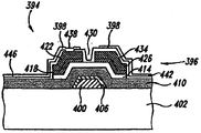
图3示出了根据一个实施方式的TFT背板的开关设备的截面图。如所示,开关设备394包括底栅型薄膜晶体管396和基于纳米结构的像素电极398。薄膜晶体管包括在衬底402上形成的栅极400。栅极可以是由光刻法限定的金属层(例如,Mo-Al-Cd)。栅绝缘层406覆盖在栅极400上面。薄膜晶体管396进一步包括绝缘层410、第一半导体层414(例如,非晶硅)和第二半导体层418(例如,n+掺杂的非晶硅),它们全部被限定成形成岛形结构。源极422和漏极426限定了沟道430,暴露出第一半导体层414(即,有源层)的一部分。另一保护层434覆盖岛形结构、源极和漏极,同时暴露出接触孔438。保护层434是例如氮化硅层。基于纳米结构的透明传导性特征442以图案的样式被涂覆在薄膜晶体管396上,以形成像素电极398。在TFT背板的其它部分中,还可以对相同的基于纳米结构的透明导体特征442进行构图,以限定信号线区446。Fig. 3 shows a cross-sectional view of a switching device of a TFT backplane according to one embodiment. As shown, the
在另一实施方式中,上文所述的开关设备可以包含到液晶显示(LCD)器件中。In another embodiment, the switching device described above may be incorporated into a liquid crystal display (LCD) device.
图4示意性示出了包括TFT背板501和滤色器衬底502的LCD器件500。背光源504将光线投射穿过偏振器508和玻璃衬底512。多条第一透明导体带520置于底部玻璃衬底512和第一对准层522(例如,聚酰亚胺层)之间。每条透明导体带520与数据线524交替设置。间隔物530设置在第一对准层522和第二对准层532之间,对准层将液晶536夹在中间。多条第二透明导体带540置于第二对准层532上,第二透明导体带540朝向与第一透明导体带520形成直角的方向。第二透明导体带540进一步涂有钝化层544、有色基质的滤色器548、顶部玻璃衬底550和偏振器554。有利地,通过分别使用对准层和被丝网印刷到底部玻璃衬底上的本文公开的透明传导性特征,可以形成透明导体带520和540。与传统使用的金属氧化物带(ITO)不同,不需要高成本的沉积处理或者蚀刻处理。FIG. 4 schematically shows an
图5示出了根据另一实施方式基于顶栅型TFT的LCD的截面图。如所示,LCD 542具有TFT衬底544和滤色器衬底546,液晶层548被插在两者之间。如上所述,在TFT衬底544中,薄膜晶体管550和像素电极552设置在底部透明衬底554上的基质构造中。公共电极556(可以向其供给公共电压)和滤色器558布置在顶部透明衬底560上。在像素电极552和公共电极556(它们彼此面对且在它们之间具有液晶548)之间施加的电压驱动液晶单元(像素)。FIG. 5 shows a cross-sectional view of a top-gate TFT-based LCD according to another embodiment. As shown, the
对于底部透明衬底554上的每个像素布置的薄膜晶体管550是顶栅型TFT,顶栅型TFT的栅极562位于有源层564之上。根据本领域公知的方法在底部衬底554上对TFT的有源层564进行构图。栅绝缘层566设置在有源层564上并且覆盖有源层564。有源层564面向栅极562的部分是沟道区564c。掺有杂质的漏区564d和源区564s置于沟道区564c的各侧面上。有源层564的漏区564d通过在覆盖栅极562的层间绝缘层568中形成的接触孔连接至数据线,数据线还起到漏极566的作用。而且,布置绝缘层570,以覆盖数据线和漏极566。形成像素电极552的、基于纳米结构的透明传导性特征置于绝缘层570上。像素电极552通过接触孔连接至有源层564的源区564s。第一对准层572可以置于像素电极上。图13进一步示出了存储电容元件574,可以对于每个像素布置存储电容元件574。当不选择TFT时,存储电容元件保持与显示内容对应的电荷,其应当被施加给液晶电容。因此,可以保持像素电极552的电压变化,使得能够在一个序列期间保持显示内容不变。如所示,有源层564的源区564s还起到存储电容元件574的第一电极576的作用。存储电容元件574的第二电极578可以与栅极562同时形成并且与栅极562形成在同一层内。栅绝缘层566还起到第一电极576和第二电极578之间的电介质的作用。栅极566(即,栅极线)和第二电极578(即,存储电容线)是平行布置的。它们朝向与像素电极552形成直角的方向,以限定像素点阵。The
应当理解,对于底栅型TFT构造和顶栅型TFT构造,有源层均可以是任何合适的半导体材料。通常,由于沉积步骤和构图步骤的方便和经济,广泛使用非晶硅。还可以使用多晶硅。由于多晶硅具有比非晶硅更强的电流驱动能力,所以当在开关器件中使用时,多晶硅提供优良的性能。多晶硅的低温沉积是可能的并且被报道为制造基于多晶硅的TFT的替换方法,参见例如第7,052,940号美国专利。此外,还可使用有机半导体材料。在某些实施方式中,有机π共轭化合物可以用作形成有机TFT的有源层的有机半导体材料。π共轭化合物是本领域公知的,其包括但不限于:聚吡咯、聚噻吩(其可选地可以掺杂有C60)、聚芘、聚乙炔和聚苯并噻吩等等。适合于有机TFT的有机半导体材料的更多示例记述在例如第7,018,872号美国专利中。It should be understood that for both the bottom-gate TFT structure and the top-gate TFT structure, the active layer can be any suitable semiconductor material. In general, amorphous silicon is widely used due to the convenience and economy of deposition steps and patterning steps. Polysilicon can also be used. Since polysilicon has a stronger current driving capability than amorphous silicon, polysilicon provides excellent performance when used in switching devices. Low temperature deposition of polysilicon is possible and reported as an alternative method for fabricating polysilicon based TFTs, see eg US Patent No. 7,052,940. In addition, organic semiconductor materials can also be used. In certain embodiments, an organic π-conjugated compound may be used as an organic semiconductor material forming an active layer of an organic TFT. [pi]-conjugated compounds are well known in the art and include, but are not limited to, polypyrrole, polythiophene (which may optionally be doped with C60 ), polypyrene, polyacetylene, and polybenzothiophene, among others. Further examples of organic semiconductor materials suitable for organic TFTs are described, for example, in US Patent No. 7,018,872.
如本文所述,TFT背板与滤色器衬底相对地置于LCD内(参见,例如图24和图25)。滤色器衬底通常包括透明衬底、黑色点阵(或者光屏蔽层)和有色像素的阵列。通常,有色像素以一定图案布置在透明衬底上。黑色点阵围绕每个有色像素形成栅格。在某些实施方式中,每个有色像素均与颜色关联。在另一些实施方式中,每个有色像素可以进一步被分成更小的着色区(称为子像素),每个子像素均与颜色关联。通常,使用原色,例如红色(R)、绿色(G)和蓝色(B)。例如,RGB三元组的重复阵列能够产生具有许多颜色的彩色图像。有色像素或者子像素不限于原色,还可以使用其它颜色,例如白色、黄色或青色。As described herein, a TFT backplane is placed within the LCD opposite the color filter substrate (see, eg, Figures 24 and 25). A color filter substrate generally includes a transparent substrate, a matrix of black dots (or a light shielding layer) and an array of colored pixels. Typically, colored pixels are arranged in a pattern on a transparent substrate. A matrix of black dots forms a grid around each colored pixel. In some embodiments, each colored pixel is associated with a color. In other embodiments, each colored pixel can be further divided into smaller colored regions (called sub-pixels), each sub-pixel being associated with a color. Typically, primary colors such as red (R), green (G) and blue (B) are used. For example, a repeating array of RGB triplets can produce a color image with many colors. Colored pixels or sub-pixels are not limited to primary colors, and other colors such as white, yellow, or cyan may also be used.
依赖于LCD的模式,在TN(扭曲向列)模式中公共电极和单元滤色器的相对位置可不同于在IPS(平面转换)模式中的相对位置。Depending on the mode of the LCD, the relative positions of the common electrode and the cell color filter in the TN (Twisted Nematic) mode may be different from those in the IPS (In-Plane Switching) mode.
(b)等离子显示板(b) Plasma display panel
等离子显示板通过用由等离子体放电产生的紫外光激发荧光材料(例如,磷光体)来发射可见光。等离子显示板使用两个绝缘衬底(例如,玻璃板),每个绝缘衬底均具有在其上形成的电极和阻隔壁,以限定单独的单元(像素)。这些单元充有一种或多种惰性气体(例如,Xe、Ne或Kr),惰性气体在电场下可被电离,以产生等离子体。更具体地,寻址电极沿着后玻璃板形成在单元后面。透明显示电极连同汇流电极一起被安装在前玻璃板上、单元前面。寻址电极和透明显示电极彼此正交并且在单元处使路径交叉。在工作时,控制电路对电极充电,在前板和后板之间形成电压差,并且使惰性气体电离并形成等离子体。The plasma display panel emits visible light by exciting a fluorescent material (eg, phosphor) with ultraviolet light generated by plasma discharge. Plasma display panels use two insulating substrates (eg, glass plates) each having electrodes and barrier walls formed thereon to define individual cells (pixels). These cells are filled with one or more noble gases (eg, Xe, Ne or Kr) that can be ionized under an electric field to generate a plasma. More specifically, address electrodes are formed behind the cells along the rear glass plate. Transparent display electrodes are mounted on the front glass plate, in front of the unit, along with bus electrodes. The address electrodes and transparent display electrodes are orthogonal to each other and intersect the paths at the cell. In operation, a control circuit charges the electrodes, creates a voltage difference between the front and rear plates, and ionizes the noble gas to form a plasma.
金属氧化物透明导体(例如,ITO)通常用作上玻璃板上的透明显示电极,以允许等离子体产生的可见光通过。基于纳米结构的透明迹线是用于PDP中的显示电极的合适电极材料。可以以所需的特征尺寸(例如,100-300μm)如本文公开的那样对它们进行丝网印刷。A metal oxide transparent conductor (eg, ITO) is generally used as a transparent display electrode on the upper glass plate to allow visible light generated by the plasma to pass through. Transparent traces based on nanostructures are suitable electrode materials for display electrodes in PDPs. They can be screen printed as disclosed herein at desired feature sizes (eg, 100-300 μm).
图6示出了根据一个实施方式的PDP的截面图。PDP 606包括:下透明衬底608;在下透明衬底608上形成的下绝缘层610;在下绝缘层608上形成的寻址电极612;在寻址电极612和下绝缘层610上形成的下介电层614;限定放电单元618的隔离壁616;置于隔离壁616上的黑色点阵层620;形成在黑色点阵层620和隔离壁616的侧面上以及下绝缘层608上的荧光层622;上透明衬底624;在上透明衬底624上形成且置于相对于寻址电极612形成直角的位置的显示电极626;在显示电极626的一部分上形成的汇流电极628;在汇流电极628、显示电极626和上透明衬底624上形成的上介电层630;以及在上介电层630上形成的保护层(例如,MgO)632。显示电极可以由根据本文描述的方法沉积的传导性纳米结构迹线来形成。FIG. 6 shows a cross-sectional view of a PDP according to one embodiment. The
应理解,基于纳米结构的透明传导性特征适合于PDP的任何其它构造,在PDP的其它构造中,透明电极置于显示板上,使得光线可以以可接受的效率传播,以在显示板上形成图像。It should be understood that nanostructure-based transparent conductive features are suitable for any other configuration of PDPs in which transparent electrodes are placed on the display panel so that light can travel with acceptable efficiency to form image.
(c)光伏电池(c) Photovoltaic cells
太阳辐射提供大约在0.4电子伏特(eV)到4电子伏特(eV)的光子范围内的可用能量。光电子器件(例如,光伏(PV)电池)可以收获此范围内的某些光子能量并将其转换成电能。光伏电池本质上是光照下的半导体结。光由半导体结(或者二极管)吸收,在结的两侧上,即在n型发射极和p型基极,产生电子-空穴对。这些电荷载流子——来自基极的电子和来自发射极的空穴——然后扩散到该结并且由电场除去,从而产生越过器件的电流。通过掺杂单种材料(例如,晶体硅)以形成P型侧和n型侧,可以在同质结电池中形成半导体结。可以使用PN结构或者P-i-N结构。Solar radiation provides usable energy in the photon range of approximately 0.4 electron volts (eV) to 4 electron volts (eV). Optoelectronic devices, such as photovoltaic (PV) cells, can harvest some of the photon energy in this range and convert it into electrical energy. Photovoltaic cells are essentially semiconductor junctions exposed to light. Light is absorbed by the semiconductor junction (or diode), and electron-hole pairs are generated on both sides of the junction, ie at the n-type emitter and p-type base. These charge carriers—electrons from the base and holes from the emitter—then diffuse to the junction and are removed by the electric field, creating a current flow across the device. A semiconductor junction can be formed in a homojunction cell by doping a single material (eg, crystalline silicon) to form a p-type side and an n-type side. A PN structure or a P-i-N structure can be used.
通过使两个不同的半导体接触,可以形成异质结。通常,这两个半导体具有不同的带隙。具有较高带隙的那个半导体因其透明度被选择并且被放置作为顶层或者窗口层。具有较低带隙的那个半导体形成底层,其用作吸光材料。窗口层允许几乎全部的入射光到达底层,底层容易地吸收光线。By bringing two different semiconductors into contact, a heterojunction can be formed. Typically, the two semiconductors have different bandgaps. The semiconductor with the higher bandgap is chosen for its transparency and placed as the top or window layer. The semiconductor with the lower bandgap forms the bottom layer, which acts as a light absorbing material. The window layer allows almost all of the incident light to reach the bottom layer, which readily absorbs light.
已经开发出多结电池,以捕获更大部分的太阳光谱。在该配置中,多个单独的异质结电池按如此方式堆叠,以至于太阳光首先落在具有最大带隙的材料上。未在第一电池中吸收的光子被传送给第二电池,第二电池于是吸收剩余太阳辐射的更高能量部分,同时对较低能量的光子保持透明。这些选择性吸收的过程继续直到最后的电池,最后的电池具有最小的带隙。Multi-junction cells have been developed to capture a larger portion of the solar spectrum. In this configuration, multiple individual heterojunction cells are stacked in such a way that sunlight falls on the material with the largest bandgap first. Photons not absorbed in the first cell are passed to the second cell, which then absorbs the higher energy portion of the remaining solar radiation, while remaining transparent to lower energy photons. These processes of selective absorption continue until the final cell, which has the smallest bandgap.
在激子PV电池中,不是p掺杂区和n掺杂区,而是具有不同带隙的材料用于分裂并且激子通过电荷从一个半导体转移到另一个半导体。在电荷分离之后,电荷因内建的电势被除去,内建的电势是由于用于电荷收集的接触电极之间的功函数的差值建立的。例如,有机光伏电池以这种方式工作,其中,一个半导体可以是聚噻吩,另一个半导体是C60。聚噻吩吸收光,产生了激子。电子从聚噻吩跳跃至C60(电子的较低能量态)。空穴沿着聚噻吩主链(backbone)移动,直到它们如电子那样通过巴基球(buckyball)之间的跳跃被收集为止。In an excitonic PV cell, instead of p-doped and n-doped regions, materials with different bandgaps are used for splitting and excitons are transferred from one semiconductor to the other by charge. After charge separation, the charges are removed due to the built-in potential established due to the difference in work function between the contact electrodes for charge collection. For example, organic photovoltaic cells work in this way, where one semiconductor can be polythiophene and the other C60. Polythiophene absorbs light, generating excitons. Electrons jump from polythiophene to C60 (lower energy state of electrons). The holes move along the polythiophene backbone until they are collected like electrons by jumping between buckyballs.
欧姆金属半导体接触设置在太阳能电池的n型侧和p型侧。在多结电池中,它们还被插在两个相邻的电池之间。在n型侧上产生的或者已经由该结“收集”并被移至n型侧上的电子可以穿过导线移动,并向负载提供功率,并且继续穿过导线,直到它们到达p型半导体-金属接触。由于透明导体(例如,ITO)允许光线穿过窗口层至下面的活性吸光材料,并且由于透明导体用作欧姆接触,以将光生电荷载流子从该吸光材料中传输走,所以它们是理想的太阳能电池的接触材料。Ohmic metal semiconductor contacts are provided on the n-type side and the p-type side of the solar cell. In multi-junction cells, they are also inserted between two adjacent cells. Electrons that are generated on the n-type side or have been "collected" by the junction and moved to the n-type side can move through the wire and provide power to a load and continue through the wire until they reach the p-type semiconductor - metal contact. Transparent conductors (e.g., ITO) are ideal because they allow light to pass through the window layer to the underlying active light-absorbing material, and because transparent conductors serve as ohmic contacts to transport photogenerated charge carriers away from the light-absorbing material Contact materials for solar cells.
图7示出了同质结太阳能电池664。太阳能电池644包括顶部接触668、底部接触670和在两者之间插入的半导体二极管672。半导体二极管可以是例如在顶部具有p掺杂的硅并在底部具有N掺杂的硅的PN结构。硅通常是晶体硅。作为更经济的可选方案,根据本领域已知的方法可以使用多晶硅。半导体二极管还可以由非晶硅形成,在该情况中,P-i-N结构是优选的。FIG. 7 shows a homojunction
顶部接触通常是光学透明的并且包括光入射表面,即光最初进入太阳能电池内的表面。可选地,衬底674可以设置在底部接触670下面。还可选地,在顶部接触上面可以形成汇流条676。汇流条676可以通过对本文所述的基于纳米结构的透明传导性线进行丝网印刷来形成。The top contact is typically optically transparent and includes the light-incident surface, ie the surface at which light initially enters the solar cell. Optionally, a
图8示出了根据另一实施方式的异质结太阳能电池。如所示,异质结太阳能电池680包括顶部接触682、底部接触684和在两者之间插入的半导体异质结层686。Fig. 8 shows a heterojunction solar cell according to another embodiment. As shown, heterojunction
在某些实施方式中,半导体异质结层686包括三层结构(例如,N-i-P)。因而,其可以包括掺杂的顶部半导体层686a、未掺杂的中间半导体层686b和掺杂的底部半导体层686c。在某些实施方式中,第一半导体层686a具有比第三半导体层686c更高的带隙。In certain embodiments, the
第一半导体层、第二半导体层和第三半导体层可以被沉积为薄膜层。适合的半导体材料包括但不限于:有机半导体材料(如本文所述的)、碲化镉(CdTe)、铜铟镓硒(CIGS)、铜铟硒(CIS)等等。例如,在典型的CdTe电池中,顶层是p型硫化镉(CdS),中间层是固有的CdTe,底层是n型碲化锌(ZnTe)。The first semiconductor layer, the second semiconductor layer and the third semiconductor layer may be deposited as thin film layers. Suitable semiconductor materials include, but are not limited to, organic semiconductor materials (as described herein), cadmium telluride (CdTe), copper indium gallium selenide (CIGS), copper indium selenide (CIS), and the like. For example, in a typical CdTe cell, the top layer is p-type cadmium sulfide (CdS), the middle layer is intrinsic CdTe, and the bottom layer is n-type zinc telluride (ZnTe).
还可能的是,在NP结构中,半导体异质结层686仅包括顶部半导体层686a和底部半导体层686c。It is also possible that, in the NP structure, the
与基于硅的太阳能电池相比,基于薄膜半导体层的异质结电池节省材料成本。然而,由于薄膜半导体层的低级性能,这种设备在能量转换方面比基于多晶硅的电池低效。因而,在一个实施方式中,结合图9描述了多结电池。如所示,多结电池690包括(顺序从上至下):顶部接触692、第一电池694、隧道层696、第二电池698和底部接触700,其中,顶部接触692和底部接触700由本文公开的基于纳米结构的透明传导性膜制成。为了简单,将多结电池690示出为仅包括两个电池。然而应当理解,可以以类似的方式制造额外的电池。Compared with silicon-based solar cells, heterojunction cells based on thin-film semiconductor layers save material costs. However, such devices are less efficient in energy conversion than polysilicon-based cells due to the inferior properties of the thin-film semiconductor layers. Thus, in one embodiment, a multi-junction cell is described in connection with FIG. 9 . As shown,
第一电池692和第二电池698具有与图29B中示出的单结太阳能电池680类似的三层结构。第一电池更接近入射光,因此应当被选择成具有比第二电池更大的带隙。在这样做的过程中,第一电池对较低能量的光子是透明的,较低能量的光子可以由第二电池698吸收。The
第一电池和第二电池由隧道层696分隔开,以允许电子在电池之间流动。隧道层696可以是PN二极管,其包括相反掺杂的半导体层。The first and second cells are separated by a
顶部接触692和底部接触700是基于纳米线的透明导体膜。它们可以通过本文描述的方法制备。本领域的技术人员将认识到,太阳能电池690可以包括额外的层,例如衬底、汇流条和防反射膜等等。此外,将理解,本文公开的基于纳米结构的透明膜适合作为任何太阳能电池配置中的一个或多个接触。
实施例Example
实施例1Example 1
银纳米线的合成Synthesis of silver nanowires
通过在存在聚乙烯吡咯烷酮(PVP)的条件下使在乙二醇中溶解的硝酸银还原,合成了银纳米线。该方法记述在例如Y.Sun、B.Gates、B.Mayers和Y.Xia的“Crystalline silver nanowires by soft solution processing(通过软溶液工艺的结晶银纳米线)”,Nanolett,(2002),2(2)165-168中。均匀的银纳米线可以通过离心法或者其它公知的方法选择性隔离。Silver nanowires were synthesized by reducing silver nitrate dissolved in ethylene glycol in the presence of polyvinylpyrrolidone (PVP). This method is described, for example, in "Crystalline silver nanowires by soft solution processing (crystallized silver nanowires by soft solution process)" by Y.Sun, B.Gates, B.Mayers and Y.Xia, Nanolett, (2002), 2( 2) 165-168. Uniform silver nanowires can be selectively isolated by centrifugation or other known methods.
可选地,通过向上述的反应混合物添加适合的离子添加剂(例如,四丁基氯化铵),可以直接合成均匀的银纳米线。可以直接使用这样产生的银纳米线,而不需要尺寸选择的独立步骤。该合成法更详细地记述在本申请的受让人Cambrios技术公司的第60/815,627号美国临时申请中,将该申请的全部内容并入本发明。Alternatively, uniform silver nanowires can be directly synthesized by adding suitable ionic additives (eg, tetrabutylammonium chloride) to the reaction mixture described above. The silver nanowires thus produced can be used directly without a separate step of size selection. This synthesis is described in more detail in US Provisional Application No. 60/815,627 of Cambrios Technologies, Inc., the assignee of the present application, the entire content of which is incorporated herein.
实施例2Example 2
传导性涂料溶液的丝网印刷;电学特性Screen printing of conductive coating solutions; electrical properties
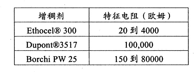
然后允许如本文所述制备的且通过沉淀和溶剂交换提纯的银纳米线在水中沉淀1周。纳米线具有大约11.5μm到15.5μm的长度,以及大约35nm到45nm的范围内的直径。将水倒出,允许沉淀纳米线充分变干。然后将PGME添加至纳米线并且混合。然后允许纳米线沉淀额外的一周,并倒出PGME。然后将结果产生的纳米线的部分分别添加给两种不同的增稠剂Dupont
通过使用AMI-Presco MSP-485丝网印刷机将每一种涂料溶液丝网印刷到透明的PET衬底上。衬底和屏之间的间隔被设置在0.010英寸到0.035英寸之间。硬度计90滚轴与250网孔不锈钢的屏一起使用。所印刷的图案是大约0.6cm宽×5.6cm长的汇流条。乳剂厚度是0.0005英寸。然后允许汇流条特征变干。然后通过使用来自Keithly
对于Ethocel
实施例3Example 3
丝网印刷传导性涂料溶液、电学特性和光学特性Screen Printing Conductive Coating Solutions, Electrical and Optical Properties
如本文描述所制备的并通过沉淀和溶剂交换提纯的银纳米线被允许在水中沉淀1周。纳米线具有大约11.5μm到15.5μm的长度和范围从大约35nm到45nm的直径。倒出水。然后将结果产生的纳米线的各部分分别添加至不同重量百分比(如下面的表2和表3所示)的PolymerInnovation


表2 Table 2

表3 table 3
如所示,对于增稠剂WB40B-63(表2)和增稠剂WB40B-64(表3),在使用了大约0.5%的增稠剂之后,特征的电阻变得相对来说很高。As shown, for thickener WB40B-63 (Table 2) and thickener WB40B-64 (Table 3), after about 0.5% thickener was used, the electrical resistance of the features became relatively high.
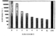
使通过使用1.25%WB40B-63增稠剂印刷的特征额外通过Pepetools Model PEPE 189.00层压机六次。每次层压之后测量电阻。此外,在六次通过层压机之后,将特征暴露于氩气环境,并再次测量电阻。层压和氩气处理的结果示出在图10中。电阻率提供在竖直轴线上,通过层压机的次数示出在水平轴线上。标有“氩”的条是氩气处理之后的电阻测量。最后的条是控制条,其既不受到层压也没有用氩气处理。如所示,在被层压六次之后,层压使特征的电阻从至少10,000kΩ减少至大约1kΩ。此外,氩气处理进一步使电阻降低至1kΩ以下。Features printed with 1.25% WB40B-63 thickener were passed through a Pepetools Model PEPE 189.00 laminator six additional times. Resistance was measured after each lamination. In addition, after six passes through the laminator, the features were exposed to an argon atmosphere and the electrical resistance was measured again. The results of lamination and argon treatment are shown in FIG. 10 . Resistivity is provided on the vertical axis and number of passes through the laminator is shown on the horizontal axis. The bar labeled "Argon" is the resistance measurement after argon treatment. The last strip was the control strip, which was neither laminated nor treated with argon. As shown, lamination reduced the resistance of the features from at least 10,000 kΩ to approximately 1 kΩ after being laminated six times. In addition, argon treatment further reduced the resistance below 1 kΩ.
在本说明书中引用的和/或在申请数据页中列举的所有上述美国专利、美国专利申请公开、美国专利申请、外国专利、外国专利申请和非专利公开通过引用全部并入本文。All of the aforementioned U.S. patents, U.S. patent application publications, U.S. patent applications, foreign patents, foreign patent applications, and non-patent publications cited in this specification and/or cited in the application data sheets are hereby incorporated by reference in their entirety.
从上述内容中将理解,虽然为了说明目的在本文中已经对本发明的特定实施方式进行了描述,但是在不背离本发明的精神和范围的条件下可以进行各种修改。因此,除了由权利要求限定之外,本发明不是限制性的。From the foregoing it will be appreciated that, although specific embodiments of the invention have been described herein for purposes of illustration, various modifications may be made without departing from the spirit and scope of the invention. Accordingly, the invention is not to be limited except as by the claims.
Claims (19)


Applications Claiming Priority (3)
| Application Number | Priority Date | Filing Date | Title |
|---|---|---|---|
| US3152808P | 2008-02-26 | 2008-02-26 | |
| US61/031,528 | 2008-02-26 | ||
| PCT/US2009/001175 WO2009108306A1 (en) | 2008-02-26 | 2009-02-25 | Method and composition for screen printing of conductive features |
Publications (2)
| Publication Number | Publication Date |
|---|---|
| CN102015921A true CN102015921A (en) | 2011-04-13 |
| CN102015921B CN102015921B (en) | 2014-08-27 |
Family
ID=40613077
Family Applications (2)
| Application Number | Title | Priority Date | Filing Date |
|---|---|---|---|
| CN2009801148130A Pending CN102015922A (en) | 2008-02-26 | 2009-02-25 | Methods and compositions for ink jet deposition of conductive features |
| CN200980114812.6A Active CN102015921B (en) | 2008-02-26 | 2009-02-25 | Method and composition for screen printing of conductive features |
Family Applications Before (1)
| Application Number | Title | Priority Date | Filing Date |
|---|---|---|---|
| CN2009801148130A Pending CN102015922A (en) | 2008-02-26 | 2009-02-25 | Methods and compositions for ink jet deposition of conductive features |
Country Status (8)
| Country | Link |
|---|---|
| US (2) | US8815126B2 (en) |
| EP (2) | EP2252662A1 (en) |
| JP (3) | JP2011515510A (en) |
| KR (2) | KR20100116680A (en) |
| CN (2) | CN102015922A (en) |
| SG (2) | SG188159A1 (en) |
| TW (2) | TWI500719B (en) |
| WO (2) | WO2009108306A1 (en) |
Cited By (8)
| Publication number | Priority date | Publication date | Assignee | Title |
|---|---|---|---|---|
| CN103021533A (en) * | 2011-09-27 | 2013-04-03 | 株式会社东芝 | transparent electrode laminate |
| CN103493149A (en) * | 2011-04-28 | 2014-01-01 | 富士胶片株式会社 | Dispersion containing metal nanowires and conductive film |
| CN103804995A (en) * | 2012-11-09 | 2014-05-21 | 财团法人工业技术研究院 | Conductive ink composition and transparent conductive film |
| CN103827984A (en) * | 2011-07-28 | 2014-05-28 | Lg伊诺特有限公司 | Electrode structure and method for making electrode |
| CN104159985A (en) * | 2012-03-08 | 2014-11-19 | 东进世美肯株式会社 | Conductive ink composition for forming transparent electrodes |
| CN104766646A (en) * | 2015-03-04 | 2015-07-08 | 江苏大学 | A high bending resistance transparent conductive film and its preparation method |
| CN105086632A (en) * | 2015-10-09 | 2015-11-25 | 重庆文理学院 | Silver conductive ink in uniform size |
| CN108690404A (en) * | 2015-10-09 | 2018-10-23 | 重庆文理学院 | A kind of water base nano silver wire conductive film preparation method of high conductivity and light transmittance |
Families Citing this family (76)
| Publication number | Priority date | Publication date | Assignee | Title |
|---|---|---|---|---|
| ATE532217T1 (en) | 2005-08-12 | 2011-11-15 | Cambrios Technologies Corp | METHOD FOR PRODUCING TRANSPARENT NANOWIRE-BASED CONDUCTORS |
| TWI426531B (en) * | 2006-10-12 | 2014-02-11 | 坎畢歐科技公司 | Transparent conductor based on nanowire and its application |
| US8018568B2 (en) | 2006-10-12 | 2011-09-13 | Cambrios Technologies Corporation | Nanowire-based transparent conductors and applications thereof |
| KR100974221B1 (en) * | 2008-04-17 | 2010-08-06 | 엘지전자 주식회사 | Selective emitter formation method of solar cell using laser annealing and manufacturing method of solar cell using same |
| WO2010095140A2 (en) * | 2009-02-23 | 2010-08-26 | Yissum Research Development Company Of The Hebrew University Of Jerusalem | Optical display device and method thereof |
| US8199044B2 (en) * | 2009-03-31 | 2012-06-12 | The United States Of America, As Represented By The Secretary Of The Navy | Artificial dielectric composites by a direct-write method |
| US20110024159A1 (en) * | 2009-05-05 | 2011-02-03 | Cambrios Technologies Corporation | Reliable and durable conductive films comprising metal nanostructures |
| JP5561714B2 (en) * | 2009-10-13 | 2014-07-30 | 日本写真印刷株式会社 | Transparent conductive film for display electrodes |
| SG10201406337UA (en) * | 2009-12-04 | 2014-11-27 | Cambrios Technologies Corp | Nanostructure-based transparent conductors having increased haze and devices comprising the same |
| JP5639463B2 (en) * | 2009-12-25 | 2014-12-10 | 富士フイルム株式会社 | Conductive composition, and transparent conductor, touch panel and solar cell using the same |
| KR101904912B1 (en) * | 2010-01-15 | 2018-10-08 | 씨에이엠 홀딩 코포레이션 | Low-haze transparent conductor |
| WO2011097470A2 (en) * | 2010-02-05 | 2011-08-11 | Cambrios Technologies Corporation | Photosensitive ink compositions and transparent conductors and method of using the same |
| WO2011106438A1 (en) * | 2010-02-24 | 2011-09-01 | Cambrios Technologies Corporation | Nanowire-based transparent conductors and methods of patterning same |
| TWI549900B (en) | 2010-03-23 | 2016-09-21 | 坎畢歐科技公司 | Patterned etching of nanostructured transparent conductors |
| JP4858652B2 (en) * | 2010-03-30 | 2012-01-18 | 大日本印刷株式会社 | Dye-sensitized solar cell |
| KR20110139941A (en) * | 2010-06-24 | 2011-12-30 | 삼성전기주식회사 | Metal ink composition and metal wiring forming method using the same, and conductive pattern formed from the metal ink composition |
| KR20110139942A (en) * | 2010-06-24 | 2011-12-30 | 삼성전기주식회사 | Metal ink composition and metal wiring forming method using the same, and conductive pattern formed from the metal ink composition |
| US9112166B2 (en) * | 2010-07-30 | 2015-08-18 | The Board Of Trustees Of The Leland Stanford Junior Univerity | Conductive films |
| KR101653031B1 (en) * | 2010-09-30 | 2016-08-31 | 미쓰비시 마테리알 가부시키가이샤 | Composition for antireflective film for solar cell, antireflective film for solar cell, method for manufacturing antireflective film for solar cell, and solar cell |
| US20120097059A1 (en) * | 2010-10-22 | 2012-04-26 | Cambrios Technologies Corporation | Nanowire ink compositions and printing of same |
| JP5450570B2 (en) * | 2010-12-03 | 2014-03-26 | 日本特殊陶業株式会社 | Method for forming conductor pattern |
| CN103338882B (en) * | 2010-12-07 | 2017-03-08 | 罗地亚管理公司 | Conductive nanostructures, methods of making the same, conductive polymer films comprising the nanostructures, and electronic devices comprising the films |
| US9184319B2 (en) | 2011-01-14 | 2015-11-10 | The Board Of Trustees Of The Leland Stanford Junior University | Multi-terminal multi-junction photovoltaic cells |
| KR20120096175A (en) | 2011-02-22 | 2012-08-30 | 엘지전자 주식회사 | Frame System for Solar Cell Module |
| US10494720B2 (en) | 2011-02-28 | 2019-12-03 | Nthdegree Technologies Worldwide Inc | Metallic nanofiber ink, substantially transparent conductor, and fabrication method |
| WO2012118582A1 (en) * | 2011-02-28 | 2012-09-07 | Nthdegree Technologies Worldwide Inc. | Metallic nanofiber ink, substantially transparent conductor, and fabrication method |
| EP2682437B8 (en) * | 2011-02-28 | 2019-10-02 | SANYO COLOR WORKS, Ltd. | Inkjet ink copolymer, inkjet ink pigment dispersing element using same, and inkjet ink |
| CN103460123B (en) | 2011-04-15 | 2016-02-10 | 3M创新有限公司 | For the transparency electrode of electronic console |
| US9603242B2 (en) | 2011-12-21 | 2017-03-21 | 3M Innovative Properties Company | Laser patterning of silver nanowire-based transparent electrically conducting coatings |
| US9441117B2 (en) * | 2012-03-20 | 2016-09-13 | Basf Se | Mixtures, methods and compositions pertaining to conductive materials |
| JP5832943B2 (en) * | 2012-03-23 | 2015-12-16 | 富士フイルム株式会社 | Conductive composition, conductive member, method for manufacturing conductive member, touch panel and solar cell |
| US10718636B1 (en) | 2012-04-11 | 2020-07-21 | Louisiana Tech Research Corporation | Magneto-resistive sensors |
| US9103654B1 (en) | 2012-04-11 | 2015-08-11 | Louisiana Tech University Research Foundation, A Division Of Louisiana Tech University Foundation, Inc. | GMR nanowire sensors |
| US9784802B1 (en) | 2012-04-11 | 2017-10-10 | Louisiana Tech Research Corporation | GMR nanowire sensors |
| US20130323482A1 (en) * | 2012-06-01 | 2013-12-05 | Nuovo Film Inc. | Low Haze Transparent Conductive Electrodes and Method of Making the Same |
| US10029916B2 (en) | 2012-06-22 | 2018-07-24 | C3Nano Inc. | Metal nanowire networks and transparent conductive material |
| US9920207B2 (en) | 2012-06-22 | 2018-03-20 | C3Nano Inc. | Metal nanostructured networks and transparent conductive material |
| US9598776B2 (en) | 2012-07-09 | 2017-03-21 | Pen Inc. | Photosintering of micron-sized copper particles |
| KR101319259B1 (en) * | 2012-07-11 | 2013-10-17 | 대한잉크 주식회사 | Silver nano wires water-based ink for a transparent electrode and method for forming the transparent electrode using the same |
| JP6700787B2 (en) | 2012-12-07 | 2020-05-27 | スリーエム イノベイティブ プロパティズ カンパニー | Method for producing transparent conductor on substrate |
| US8957322B2 (en) * | 2012-12-07 | 2015-02-17 | Cambrios Technologies Corporation | Conductive films having low-visibility patterns and methods of producing the same |
| WO2014116738A1 (en) | 2013-01-22 | 2014-07-31 | Cambrios Technologies Corporation | Nanostructure transparent conductors having high thermal stability for esd protection |
| US10720257B2 (en) | 2013-02-15 | 2020-07-21 | Cambrios Film Solutions Corporation | Methods to incorporate silver nanowire-based transparent conductors in electronic devices |
| EP2956807B1 (en) | 2013-02-15 | 2021-11-03 | Cambrios Film Solutions Corporation | Methods to incorporate silver nanowire-based transparent conductors in electronic devices |
| US10971277B2 (en) | 2013-02-15 | 2021-04-06 | Cambrios Film Solutions Corporation | Methods to incorporate silver nanowire-based transparent conductors in electronic devices |
| US10020807B2 (en) | 2013-02-26 | 2018-07-10 | C3Nano Inc. | Fused metal nanostructured networks, fusing solutions with reducing agents and methods for forming metal networks |
| US20140262443A1 (en) * | 2013-03-14 | 2014-09-18 | Cambrios Technologies Corporation | Hybrid patterned nanostructure transparent conductors |
| US9368248B2 (en) | 2013-04-05 | 2016-06-14 | Nuovo Film, Inc. | Transparent conductive electrodes comprising metal nanowires, their structure design, and method of making such structures |
| JP2014224199A (en) * | 2013-05-16 | 2014-12-04 | Dowaエレクトロニクス株式会社 | Production method for silver nanowire ink, and silver nanowire ink |
| KR102169003B1 (en) * | 2013-06-20 | 2020-10-22 | 주식회사 잉크테크 | Conductive ink composition, transparent conductive film comprising thereof and method for preparing transparent conductive film |
| SG10201808518RA (en) * | 2013-07-31 | 2018-10-30 | 3M Innovative Properties Co | Bonding electronic components to patterned nanowire transparent conductors |
| CN105474760B (en) | 2013-08-28 | 2019-03-08 | 3M创新有限公司 | Electronic assembly with fiducial marks for precise registration |
| US9759846B2 (en) | 2013-09-27 | 2017-09-12 | Cam Holding Corporation | Silver nanostructure-based optical stacks and touch sensors with UV protection |
| KR20150034993A (en) * | 2013-09-27 | 2015-04-06 | 주식회사 동진쎄미켐 | Conductive coating composition containing metallic nanowires and forming method for conductive film using the same |
| US11274223B2 (en) | 2013-11-22 | 2022-03-15 | C3 Nano, Inc. | Transparent conductive coatings based on metal nanowires and polymer binders, solution processing thereof, and patterning approaches |
| US9773989B2 (en) * | 2013-12-03 | 2017-09-26 | National University Corporation Yamagata University | Method for producing metal thin film and conductive structure |
| US11343911B1 (en) | 2014-04-11 | 2022-05-24 | C3 Nano, Inc. | Formable transparent conductive films with metal nanowires |
| CN103965683B (en) * | 2014-05-22 | 2016-06-29 | 厦门市豪尔新材料股份有限公司 | Integration touch-control touch screen protective acid-proof ink and preparation method thereof |
| PL2960310T3 (en) | 2014-06-27 | 2017-02-28 | Henkel Ag & Co. Kgaa | Conductive transparent coating for rigid and flexible substrates |
| US9183968B1 (en) | 2014-07-31 | 2015-11-10 | C3Nano Inc. | Metal nanowire inks for the formation of transparent conductive films with fused networks |
| JP2016058319A (en) * | 2014-09-11 | 2016-04-21 | デクセリアルズ株式会社 | ELECTRODE, ITS MANUFACTURING METHOD, TOUCH PANEL EQUIPPED WITH THE ELECTRODE AND ORGANIC EL SUBSTRATE |
| KR101930385B1 (en) * | 2014-11-05 | 2018-12-18 | 씨에이엠 홀딩 코포레이션 | Short-chain fluorosurfactants with iodide additives for forming silver nanowire-based transparent conductive films |
| GB2535214A (en) * | 2015-02-13 | 2016-08-17 | Dst Innovation Ltd | Printable conductive ink and method of forming transparent printed electrodes |
| EP3118265A1 (en) * | 2015-07-14 | 2017-01-18 | Henkel AG & Co. KGaA | Conductive transparent coating |
| CN105153813B (en) * | 2015-09-22 | 2018-09-14 | 华南理工大学 | A kind of preparation method of low percolation threshold electrically conductive ink |
| USRE49626E1 (en) * | 2015-12-29 | 2023-08-29 | Universidade Do Minho | Piezoresistive ink, methods and uses thereof |
| DE102017100898A1 (en) | 2017-01-18 | 2018-07-19 | Osram Oled Gmbh | Inkjet printable composition, organic light emitting device and method of making the organic light emitting device |
| EP3616905A4 (en) * | 2017-03-27 | 2021-04-28 | Kuraray Co., Ltd. | POLYACETAL VINYL RESIN FILM FOR LAMINATED GLASS |
| TWI711058B (en) * | 2017-08-09 | 2020-11-21 | 日商新烯控股有限公司 | Manufacturing method and device of electronic component and electronic component |
| CN110534256B (en) * | 2018-05-23 | 2021-04-02 | 睿明科技股份有限公司 | Manufacturing method of conductive film |
| CN108976914B (en) * | 2018-08-14 | 2021-06-22 | 重庆文理学院 | A kind of highly dispersed copper nanowire conductive ink, conductive film and preparation method thereof |
| US12263529B2 (en) | 2019-04-03 | 2025-04-01 | Pine Castle Investments Limited | Conductive nanostructure purification |
| WO2021094901A1 (en) | 2019-11-15 | 2021-05-20 | 3M Innovative Properties Company | Expandable microsphere, markable article, marked article, and method of making the same |
| JP7464378B2 (en) * | 2019-11-22 | 2024-04-09 | 住友重機械工業株式会社 | Ink application control device and ink application method |
| CN111154330B (en) * | 2020-02-28 | 2022-05-03 | 苏州世华新材料科技股份有限公司 | Heat-conducting insulating ink, preparation method and application thereof to copper foil adhesive tape |
| KR102901953B1 (en) * | 2020-12-30 | 2025-12-18 | 엘지디스플레이 주식회사 | Display panel and display device |
Citations (4)
| Publication number | Priority date | Publication date | Assignee | Title |
|---|---|---|---|---|
| CN1403516A (en) * | 2002-07-02 | 2003-03-19 | 田桂英 | Anticorrosive composite paint and its prepn and application |
| CN1425047A (en) * | 1999-11-25 | 2003-06-18 | 西柏控股有限公司 | Printing ink, micro-filaments used as antenna in antifakery document and methods for producing antifakery document and idenlifying document |
| WO2007022226A2 (en) * | 2005-08-12 | 2007-02-22 | Cambrios Technologies Corporation | Nanowires-based transparent conductors |
| EP1769867A1 (en) * | 2004-07-08 | 2007-04-04 | Mitsubishi Materials Corporation | Method for producing metal fine particle, metal fine particle produced thereby, composition containing same, light absorbing material, and application thereof |
Family Cites Families (48)
| Publication number | Priority date | Publication date | Assignee | Title |
|---|---|---|---|---|
| DE19503281A1 (en) * | 1995-02-02 | 1996-08-08 | Bayer Ag | Polyurethanes suitable as thickeners for aqueous systems |
| KR970073821A (en) | 1995-09-27 | 1997-12-10 | 아키모토 유미 | Manufacturing method and apparatus of porous sintered metal plate |
| US7098163B2 (en) | 1998-08-27 | 2006-08-29 | Cabot Corporation | Method of producing membrane electrode assemblies for use in proton exchange membrane and direct methanol fuel cells |
| US6436180B1 (en) | 2000-03-31 | 2002-08-20 | Hewlett-Packard Company | Color ink composition for graphic art ink jet image printers |
| JP2003043238A (en) * | 2001-07-27 | 2003-02-13 | Canon Inc | Color filter, method of manufacturing the same, and liquid crystal device using the color filter |
| EP1361619A3 (en) | 2002-05-09 | 2007-08-15 | Konica Corporation | Organic thin-film transistor, organic thin-film transistor sheet and manufacturing method thereof |
| US7566360B2 (en) | 2002-06-13 | 2009-07-28 | Cima Nanotech Israel Ltd. | Nano-powder-based coating and ink compositions |
| EP2154212A1 (en) | 2002-06-13 | 2010-02-17 | Cima Nano Tech Israel Ltd | A method for the production of conductive and transparent nano-coatings |
| JP3842177B2 (en) | 2002-07-03 | 2006-11-08 | 独立行政法人科学技術振興機構 | Noble metal nanotube and method for producing the same |
| KR20060012545A (en) | 2002-07-03 | 2006-02-08 | 나노파우더스 인더스트리어스 리미티드. | Low temperature sintered conductive nano ink and its manufacturing method |
| KR20040021758A (en) | 2002-09-04 | 2004-03-11 | 엘지.필립스 엘시디 주식회사 | Method for fabricating of a poly-Si TFT |
| JP2004127676A (en) * | 2002-10-01 | 2004-04-22 | Seiko Epson Corp | Wiring pattern ink, wiring pattern forming method, conductive film wiring, electro-optical device, and electronic equipment |
| JP2004196912A (en) * | 2002-12-17 | 2004-07-15 | Toyobo Co Ltd | Conductive coating |
| JP4341005B2 (en) | 2002-12-17 | 2009-10-07 | 三菱マテリアル株式会社 | Metal nanowire-containing composition and electromagnetic wave shielding filter |
| US6975067B2 (en) | 2002-12-19 | 2005-12-13 | 3M Innovative Properties Company | Organic electroluminescent device and encapsulation method |
| JP3994156B2 (en) * | 2003-01-27 | 2007-10-17 | 独立行政法人産業技術総合研究所 | Metal nanowire production method and precursor for metal nanowire production |
| US7211205B2 (en) * | 2003-01-29 | 2007-05-01 | Parelec, Inc. | High conductivity inks with improved adhesion |
| US7097788B2 (en) * | 2003-06-30 | 2006-08-29 | The Board Of Trustees Of The University Of Illinois | Conducting inks |
| US7062848B2 (en) * | 2003-09-18 | 2006-06-20 | Hewlett-Packard Development Company, L.P. | Printable compositions having anisometric nanostructures for use in printed electronics |
| US7618704B2 (en) | 2003-09-29 | 2009-11-17 | E.I. Du Pont De Nemours And Company | Spin-printing of electronic and display components |
| JP2005126664A (en) | 2003-09-30 | 2005-05-19 | Mitsuboshi Belting Ltd | Treating agent for forming thin film and method for forming thin film |
| JP4800609B2 (en) | 2003-12-12 | 2011-10-26 | 藤倉化成株式会社 | Conductive paste, conductive sheet and method for producing the same |
| US20050173680A1 (en) | 2004-02-10 | 2005-08-11 | Haixin Yang | Ink jet printable thick film ink compositions and processes |
| US20050197419A1 (en) * | 2004-03-03 | 2005-09-08 | Graziano Louis C. | Radiation curable aqueous binders for ink jet inks |
| US7211135B2 (en) | 2004-03-16 | 2007-05-01 | Nanogate Coating Systems Gmbh | Writable and printable colloidal gold solution |
| KR20060129090A (en) | 2004-04-16 | 2006-12-14 | 도쿠리츠교세이호징 붓시쯔 자이료 겐큐키코 | Metal particulate colloidal solution, conductive paste material, conductive ink material and their manufacturing method |
| JP4529160B2 (en) | 2004-07-08 | 2010-08-25 | 三菱マテリアル株式会社 | METAL PARTICLE, PROCESS FOR PRODUCING THE SAME, COMPOSITION CONTAINING THE SAME AND USE THEREOF |
| US20060130700A1 (en) * | 2004-12-16 | 2006-06-22 | Reinartz Nicole M | Silver-containing inkjet ink |
| CN101102905B (en) | 2005-01-14 | 2011-01-12 | 卡伯特公司 | Security feature, use thereof and method of manufacture |
| TW200640596A (en) | 2005-01-14 | 2006-12-01 | Cabot Corp | Production of metal nanoparticles |
| JP2006219625A (en) | 2005-02-14 | 2006-08-24 | Ricoh Printing Systems Ltd | Ink for ink-jet recording, ink-jet recording device, ink-jet recording method and ink-jet recorded material |
| JP4821951B2 (en) | 2005-02-23 | 2011-11-24 | 三菱マテリアル株式会社 | Wire-shaped gold fine particles, production method thereof, containing composition and use |
| US20060199877A1 (en) * | 2005-03-01 | 2006-09-07 | Sivapackia Ganapathiappan | Shear stable latex particles |
| JP2006294550A (en) * | 2005-04-14 | 2006-10-26 | Osaka Prefecture Univ | Conductive ink for printed circuit board wiring and printed circuit board wiring method |
| JP2006307046A (en) * | 2005-04-28 | 2006-11-09 | Toppan Forms Co Ltd | Ink jet ink detectable by X-ray and sheet using the same |
| JP2007230021A (en) * | 2006-02-28 | 2007-09-13 | Ricoh Co Ltd | RECORDING INK, RECORDING MEDIUM SET, INK CARTRIDGE, AND INKJET RECORDING METHOD |
| JP2007194174A (en) | 2006-01-23 | 2007-08-02 | Seiko Epson Corp | Conductor pattern ink, conductor pattern, wiring board, electro-optical device, and electronic device |
| JP2007291239A (en) * | 2006-04-25 | 2007-11-08 | Konica Minolta Medical & Graphic Inc | Ink for preventing forgery |
| TWI397446B (en) | 2006-06-21 | 2013-06-01 | Cambrios Technologies Corp | Methods of controlling nanostructure formations and shapes |
| US7630041B2 (en) | 2006-06-23 | 2009-12-08 | Tsinghua University | Liquid crystal cell assembly for liquid crystal display |
| US8481161B2 (en) * | 2006-06-28 | 2013-07-09 | Samsung Electronics Co., Ltd. | Functionalized metal nanoparticle and method for formation of conductive pattern using the same |
| TWI426531B (en) | 2006-10-12 | 2014-02-11 | 坎畢歐科技公司 | Transparent conductor based on nanowire and its application |
| WO2008147431A2 (en) | 2006-10-12 | 2008-12-04 | Cambrios Technologies Corporation | Functional films formed by highly oriented deposition of nanowires |
| TWI550646B (en) | 2006-10-12 | 2016-09-21 | 坎畢歐科技公司 | Method of manufacturing a transparent conductor |
| JP2008198595A (en) | 2007-01-16 | 2008-08-28 | Mitsubishi Chemicals Corp | Metal fine particle ink paste and organic acid-treated metal fine particle |
| JP5085372B2 (en) * | 2007-03-13 | 2012-11-28 | 東海ゴム工業株式会社 | Paste material |
| CN103777417B (en) | 2007-04-20 | 2017-01-18 | 凯姆控股有限公司 | Composite transparent conductors and methods of forming the same |
| US20090035707A1 (en) * | 2007-08-01 | 2009-02-05 | Yubing Wang | Rheology-controlled conductive materials, methods of production and uses thereof |
-
2009
- 2009-02-25 SG SG2013011432A patent/SG188159A1/en unknown
- 2009-02-25 JP JP2010548706A patent/JP2011515510A/en active Pending
- 2009-02-25 SG SG2013011424A patent/SG188158A1/en unknown
- 2009-02-25 EP EP09713701A patent/EP2252662A1/en not_active Withdrawn
- 2009-02-25 KR KR1020107021161A patent/KR20100116680A/en not_active Ceased
- 2009-02-25 US US12/380,294 patent/US8815126B2/en active Active
- 2009-02-25 JP JP2010548705A patent/JP2011513534A/en active Pending
- 2009-02-25 EP EP09714021A patent/EP2252663A1/en not_active Withdrawn
- 2009-02-25 WO PCT/US2009/001175 patent/WO2009108306A1/en not_active Ceased
- 2009-02-25 KR KR1020107020454A patent/KR20100125315A/en not_active Ceased
- 2009-02-25 WO PCT/US2009/001169 patent/WO2009108304A1/en not_active Ceased
- 2009-02-25 US US12/380,293 patent/US8632700B2/en not_active Expired - Fee Related
- 2009-02-25 CN CN2009801148130A patent/CN102015922A/en active Pending
- 2009-02-25 TW TW098106223A patent/TWI500719B/en not_active IP Right Cessation
- 2009-02-25 TW TW098106226A patent/TWI500713B/en not_active IP Right Cessation
- 2009-02-25 CN CN200980114812.6A patent/CN102015921B/en active Active
-
2014
- 2014-10-06 JP JP2014205565A patent/JP2015045006A/en active Pending
Patent Citations (4)
| Publication number | Priority date | Publication date | Assignee | Title |
|---|---|---|---|---|
| CN1425047A (en) * | 1999-11-25 | 2003-06-18 | 西柏控股有限公司 | Printing ink, micro-filaments used as antenna in antifakery document and methods for producing antifakery document and idenlifying document |
| CN1403516A (en) * | 2002-07-02 | 2003-03-19 | 田桂英 | Anticorrosive composite paint and its prepn and application |
| EP1769867A1 (en) * | 2004-07-08 | 2007-04-04 | Mitsubishi Materials Corporation | Method for producing metal fine particle, metal fine particle produced thereby, composition containing same, light absorbing material, and application thereof |
| WO2007022226A2 (en) * | 2005-08-12 | 2007-02-22 | Cambrios Technologies Corporation | Nanowires-based transparent conductors |
Cited By (10)
| Publication number | Priority date | Publication date | Assignee | Title |
|---|---|---|---|---|
| CN103493149A (en) * | 2011-04-28 | 2014-01-01 | 富士胶片株式会社 | Dispersion containing metal nanowires and conductive film |
| CN103493149B (en) * | 2011-04-28 | 2015-11-25 | 富士胶片株式会社 | Dispersion containing metal nanowires and conductive film |
| CN103827984A (en) * | 2011-07-28 | 2014-05-28 | Lg伊诺特有限公司 | Electrode structure and method for making electrode |
| CN103021533A (en) * | 2011-09-27 | 2013-04-03 | 株式会社东芝 | transparent electrode laminate |
| CN104159985A (en) * | 2012-03-08 | 2014-11-19 | 东进世美肯株式会社 | Conductive ink composition for forming transparent electrodes |
| CN104159985B (en) * | 2012-03-08 | 2016-11-09 | 东进世美肯株式会社 | Transparency electrode formation conductive ink composition |
| CN103804995A (en) * | 2012-11-09 | 2014-05-21 | 财团法人工业技术研究院 | Conductive ink composition and transparent conductive film |
| CN104766646A (en) * | 2015-03-04 | 2015-07-08 | 江苏大学 | A high bending resistance transparent conductive film and its preparation method |
| CN105086632A (en) * | 2015-10-09 | 2015-11-25 | 重庆文理学院 | Silver conductive ink in uniform size |
| CN108690404A (en) * | 2015-10-09 | 2018-10-23 | 重庆文理学院 | A kind of water base nano silver wire conductive film preparation method of high conductivity and light transmittance |
Also Published As
| Publication number | Publication date |
|---|---|
| CN102015922A (en) | 2011-04-13 |
| TWI500719B (en) | 2015-09-21 |
| EP2252663A1 (en) | 2010-11-24 |
| WO2009108306A1 (en) | 2009-09-03 |
| TW200946608A (en) | 2009-11-16 |
| KR20100125315A (en) | 2010-11-30 |
| JP2015045006A (en) | 2015-03-12 |
| EP2252662A1 (en) | 2010-11-24 |
| TW200946617A (en) | 2009-11-16 |
| SG188158A1 (en) | 2013-03-28 |
| JP2011513534A (en) | 2011-04-28 |
| WO2009108304A1 (en) | 2009-09-03 |
| TWI500713B (en) | 2015-09-21 |
| US8815126B2 (en) | 2014-08-26 |
| US20090223703A1 (en) | 2009-09-10 |
| CN102015921B (en) | 2014-08-27 |
| KR20100116680A (en) | 2010-11-01 |
| SG188159A1 (en) | 2013-03-28 |
| US20090283304A1 (en) | 2009-11-19 |
| US8632700B2 (en) | 2014-01-21 |
| JP2011515510A (en) | 2011-05-19 |
Similar Documents
| Publication | Publication Date | Title |
|---|---|---|
| CN102015921B (en) | Method and composition for screen printing of conductive features | |
| JP2011515510A5 (en) | ||
| KR101545219B1 (en) | Nanowire-based transparent conductors and their applications | |
| US8174667B2 (en) | Nanowire-based transparent conductors and applications thereof | |
| KR102154562B1 (en) | Nanostructure-based transparent conductors having increased haze and devices comprising the same | |
| KR20130048717A (en) | Nanowire-based transparent conductors and methods of patterning same | |
| US20140290987A1 (en) | Solution processed nanoparticle-nanowire composite film as a transparent conductor for opto-electronic devices | |
| US20140262443A1 (en) | Hybrid patterned nanostructure transparent conductors | |
| HK1133326A (en) | Nanowire-based transparent conductors and applications thereof | |
| HK1133326B (en) | Nanowire-based transparent conductors and applications thereof |
Legal Events
| Date | Code | Title | Description |
|---|---|---|---|
| C06 | Publication | ||
| PB01 | Publication | ||
| C10 | Entry into substantive examination | ||
| SE01 | Entry into force of request for substantive examination | ||
| C14 | Grant of patent or utility model | ||
| GR01 | Patent grant | ||
| C41 | Transfer of patent application or patent right or utility model | ||
| TR01 | Transfer of patent right |
Effective date of registration: 20160928 Address after: Virgin Islands Patentee after: CAM HOLDING Corp. Address before: Island of Eden, Republic of Seychelles Patentee before: Guanwei International Co.,Ltd. Effective date of registration: 20160928 Address after: Island of Eden, Republic of Seychelles Patentee after: Guanwei International Co.,Ltd. Address before: California, USA Patentee before: CAMBRIOS TECHNOLOGIES Corp. |
|
| CP01 | Change in the name or title of a patent holder | ||
| CP01 | Change in the name or title of a patent holder |
Address after: Virgin Islands Patentee after: British Virgin Islands Shangtiancai Innovative Materials Technology Co.,Ltd. Address before: Virgin Islands Patentee before: CAM HOLDING Corp. |
|
| EE01 | Entry into force of recordation of patent licensing contract |
Application publication date: 20110413 Assignee: NUOVO FILM SUZHOU CHINA Inc. Assignor: British Virgin Islands Shangtiancai Innovative Materials Technology Co.,Ltd. Contract record no.: 2018990000341 Denomination of invention: Method and composition for screen printing of conductive features Granted publication date: 20140827 License type: Exclusive License Record date: 20181210 |
|
| EE01 | Entry into force of recordation of patent licensing contract | ||
| EC01 | Cancellation of recordation of patent licensing contract |
Assignee: NUOVO FILM SUZHOU CHINA Inc. Assignor: British Virgin Islands Shangtiancai Innovative Materials Technology Co.,Ltd. Contract record no.: 2018990000341 Date of cancellation: 20240717 |
|
| EC01 | Cancellation of recordation of patent licensing contract | ||
| EE01 | Entry into force of recordation of patent licensing contract |
Application publication date: 20110413 Assignee: NUOVO FILM SUZHOU CHINA Inc. Assignor: British Virgin Islands Shangtiancai Innovative Materials Technology Co.,Ltd. Contract record no.: X2024990000389 Denomination of invention: Method and composition for screen printing conductive features Granted publication date: 20140827 License type: Exclusive License Record date: 20240731 |
|
| EE01 | Entry into force of recordation of patent licensing contract | ||
| TR01 | Transfer of patent right |
Effective date of registration: 20250217 Address after: Rhode City, Tortola Island, British Virgin Islands Patentee after: Songbao Investment Co.,Ltd. Country or region after: British Virgin Islands Address before: Tortola Island, Virgin Islands Patentee before: British Virgin Islands Shangtiancai Innovative Materials Technology Co.,Ltd. Country or region before: British Virgin Islands |
|
| TR01 | Transfer of patent right |