CN101951470B - Solid-state imaging device and imaging apparatus - Google Patents
Solid-state imaging device and imaging apparatus Download PDFInfo
- Publication number
- CN101951470B CN101951470B CN2010101407816A CN201010140781A CN101951470B CN 101951470 B CN101951470 B CN 101951470B CN 2010101407816 A CN2010101407816 A CN 2010101407816A CN 201010140781 A CN201010140781 A CN 201010140781A CN 101951470 B CN101951470 B CN 101951470B
- Authority
- CN
- China
- Prior art keywords
- receiving unit
- light receiving
- pixels
- optical waveguide
- imaging device
- Prior art date
- Legal status (The legal status is an assumption and is not a legal conclusion. Google has not performed a legal analysis and makes no representation as to the accuracy of the status listed.)
- Expired - Fee Related
Links
Images


Classifications
-
- H—ELECTRICITY
- H10—SEMICONDUCTOR DEVICES; ELECTRIC SOLID-STATE DEVICES NOT OTHERWISE PROVIDED FOR
- H10F—INORGANIC SEMICONDUCTOR DEVICES SENSITIVE TO INFRARED RADIATION, LIGHT, ELECTROMAGNETIC RADIATION OF SHORTER WAVELENGTH OR CORPUSCULAR RADIATION
- H10F77/00—Constructional details of devices covered by this subclass
- H10F77/40—Optical elements or arrangements
-
- H—ELECTRICITY
- H04—ELECTRIC COMMUNICATION TECHNIQUE
- H04N—PICTORIAL COMMUNICATION, e.g. TELEVISION
- H04N25/00—Circuitry of solid-state image sensors [SSIS]; Control thereof
- H04N25/70—SSIS architectures; Circuits associated therewith
- H04N25/76—Addressed sensors, e.g. MOS or CMOS sensors
- H04N25/77—Pixel circuitry, e.g. memories, A/D converters, pixel amplifiers, shared circuits or shared components
- H04N25/778—Pixel circuitry, e.g. memories, A/D converters, pixel amplifiers, shared circuits or shared components comprising amplifiers shared between a plurality of pixels, i.e. at least one part of the amplifier must be on the sensor array itself
-
- H—ELECTRICITY
- H10—SEMICONDUCTOR DEVICES; ELECTRIC SOLID-STATE DEVICES NOT OTHERWISE PROVIDED FOR
- H10F—INORGANIC SEMICONDUCTOR DEVICES SENSITIVE TO INFRARED RADIATION, LIGHT, ELECTROMAGNETIC RADIATION OF SHORTER WAVELENGTH OR CORPUSCULAR RADIATION
- H10F39/00—Integrated devices, or assemblies of multiple devices, comprising at least one element covered by group H10F30/00, e.g. radiation detectors comprising photodiode arrays
- H10F39/80—Constructional details of image sensors
- H10F39/805—Coatings
- H10F39/8057—Optical shielding
-
- H—ELECTRICITY
- H10—SEMICONDUCTOR DEVICES; ELECTRIC SOLID-STATE DEVICES NOT OTHERWISE PROVIDED FOR
- H10F—INORGANIC SEMICONDUCTOR DEVICES SENSITIVE TO INFRARED RADIATION, LIGHT, ELECTROMAGNETIC RADIATION OF SHORTER WAVELENGTH OR CORPUSCULAR RADIATION
- H10F39/00—Integrated devices, or assemblies of multiple devices, comprising at least one element covered by group H10F30/00, e.g. radiation detectors comprising photodiode arrays
- H10F39/80—Constructional details of image sensors
- H10F39/806—Optical elements or arrangements associated with the image sensors
- H10F39/8067—Reflectors
-
- H—ELECTRICITY
- H10—SEMICONDUCTOR DEVICES; ELECTRIC SOLID-STATE DEVICES NOT OTHERWISE PROVIDED FOR
- H10F—INORGANIC SEMICONDUCTOR DEVICES SENSITIVE TO INFRARED RADIATION, LIGHT, ELECTROMAGNETIC RADIATION OF SHORTER WAVELENGTH OR CORPUSCULAR RADIATION
- H10F39/00—Integrated devices, or assemblies of multiple devices, comprising at least one element covered by group H10F30/00, e.g. radiation detectors comprising photodiode arrays
- H10F39/80—Constructional details of image sensors
- H10F39/813—Electronic components shared by multiple pixels, e.g. one amplifier shared by two pixels
Landscapes
- Engineering & Computer Science (AREA)
- Multimedia (AREA)
- Signal Processing (AREA)
- Solid State Image Pick-Up Elements (AREA)
- Transforming Light Signals Into Electric Signals (AREA)
Abstract
本发明提供了固态成像器件和成像装置。一种成像器件包括基本单元,该基本单元具有共享浮置扩散区的两个或更多个像素。该成像器件还包括被基本单元中的两个或更多个像素所共享并被布置在两个或更多个像素的外部的晶体管。该成像器件还包括光接收单元,其通过传输栅被连接到被基本单元中的像素所共享的浮置扩散区。在该成像器件中,片上透镜被基本上等间距布置。而且,光波导被形成为使得其在固态成像器件的表面中的位置位于从光接收单元的中心向晶体管移位的位置上并且位于光接收单元之内和片上透镜之内。

The present invention provides a solid-state imaging device and an imaging device. An imaging device includes a base unit having two or more pixels sharing a floating diffusion region. The imaging device further includes a transistor shared by two or more pixels in the basic unit and arranged outside the two or more pixels. The imaging device also includes a light receiving unit connected to a floating diffusion area shared by pixels in the basic unit through a transfer gate. In this imaging device, on-chip lenses are arranged at substantially equal intervals. Also, the optical waveguide is formed such that its position in the surface of the solid-state imaging device is at a position displaced from the center of the light receiving unit toward the transistor and is located inside the light receiving unit and inside the on-chip lens.
Description
技术领域 technical field
本发明涉及光接收单元上具有光波导(optical waveguide)的固态成像器件并且还涉及具有该固态成像器件的成像装置。The present invention relates to a solid-state imaging device having an optical waveguide on a light receiving unit and also relates to an imaging apparatus having the solid-state imaging device.
背景技术 Background technique
在固态成像器件中,从成像器件中心到像素的距离增大得越多,像素上光的入射角度增大得越多。因此,如果最上面的透镜刚好位于光电转换单元(光接收单元)的上方,则入射在光电转换单元(光接收单元)上的光量减小。In a solid-state imaging device, the more the distance from the center of the imaging device to the pixel increases, the more the incident angle of light on the pixel increases. Therefore, if the uppermost lens is positioned just above the photoelectric conversion unit (light receiving unit), the amount of light incident on the photoelectric conversion unit (light receiving unit) decreases.
因此,建议了如下固态成像器件:其中,每个透镜和光电转换单元(光接收单元)的水平位置取决于从成像器件中心到像素的距离而移位,以将透镜布置在成像器件中心附近(例如,参见日本专利早期公开No.2006-261247、No.2006-261249和No.2006-324439)。这种成像器件的配置可以允许穿过透镜的倾斜入射光的更多光量进入光电转换单元(光接收单元),从而产生足够的灵敏度。这种方式的结构组件(例如透镜和光接收单元)的水平位置的移位被称为“光瞳校正(pupil correction)”。换言之,术语“光瞳校正”指片上透镜被移位到适当位置来针对下述情况采取措施:入射光不是垂直入射而是倾斜入射到像素外围。Therefore, a solid-state imaging device has been proposed in which the horizontal position of each lens and photoelectric conversion unit (light receiving unit) is shifted depending on the distance from the center of the imaging device to the pixel to arrange the lens near the center of the imaging device ( For example, see Japanese Patent Laid-Open Publication No. 2006-261247, No. 2006-261249 and No. 2006-324439). The configuration of such an imaging device can allow a larger amount of obliquely incident light passing through the lens to enter the photoelectric conversion unit (light receiving unit), resulting in sufficient sensitivity. Shifting the horizontal position of structural components such as lenses and light receiving units in this manner is called "pupil correction". In other words, the term "pupil correction" means that the on-chip lens is shifted to an appropriate position to take measures against the case where incident light is not perpendicularly incident but obliquely incident to the periphery of the pixel.
此外,在日本专利早期公开No.2006-261249中,在透镜和光接收单元之间提供了光波导。然后,透镜、光波导和光接收单元在水平方向上移位,以使得从成像器件中心到透镜、光波导和光接收单元的距离按此顺序随着从成像器件中心到像素距离的增大而增大。Furthermore, in Japanese Patent Laid-Open No. 2006-261249, an optical waveguide is provided between the lens and the light receiving unit. Then, the lens, the optical waveguide, and the light-receiving unit are displaced in the horizontal direction, so that the distances from the center of the imaging device to the lens, the optical waveguide, and the light-receiving unit increase in this order as the distance from the center of the imaging device to the pixel increases .
另外,在典型的CMOS型固态成像器件中,针对每个像素提供了晶体管和浮置扩散区(floating diffusion)。每个像素中晶体管和浮置扩散区的存在限制了更精细像素的生产。像素被制造得越精细,光接收单元的表面积则减小得越多。结果,发生电荷量的减少。因此,所生产的像素可能是非常暗的像素,并且还可能有随机噪声与图像信号重叠。In addition, in a typical CMOS type solid-state imaging device, a transistor and a floating diffusion are provided for each pixel. The presence of transistors and floating diffusions in each pixel limits the production of finer pixels. The finer the pixels are made, the more the surface area of the light receiving unit is reduced. As a result, a decrease in the charge amount occurs. Therefore, the pixels produced may be very dark pixels and may also have random noise overlapping the image signal.
为了避免这种现象,建议了另一成像器件:其中,晶体管和浮置扩散区被两个或更多个像素所共享以减小由这些元件所占据的像素的表面积,同时增大由光接收单元所占据的像素的表面积(例如,参见日本专利早期公开No.2006-303468)。In order to avoid this phenomenon, another imaging device has been proposed in which a transistor and a floating diffusion region are shared by two or more pixels to reduce the surface area of the pixel occupied by these elements while increasing the area received by light. The surface area of a pixel occupied by a cell (for example, see Japanese Patent Laid-Open No. 2006-303468).
发明内容 Contents of the invention
光波导的形成包括在其内部埋入材料的步骤。但是,如果像素被制造得很精细,则光波导的开口尺寸被制造得较小。这由于制造过程中生成气泡等而导致埋入光波导过程的质量下降。因此,在具有光波导的像素的小型化方面存在限制。因此,如上所述埋入光波导过程的质量下降使得在各个像素中埋入光波导过程的质量存在很大差异,从而导致像素制造产量的下降。Formation of an optical waveguide includes the step of embedding material within it. However, if the pixel is made fine, the opening size of the optical waveguide is made smaller. This degrades the quality of the process of embedding the optical waveguide due to the generation of air bubbles and the like during the manufacturing process. Therefore, there is a limit in the miniaturization of pixels with optical waveguides. Therefore, the degradation of the process of embedding the optical waveguide as described above causes a large difference in the quality of the process of embedding the optical waveguide in each pixel, resulting in a decrease in pixel manufacturing yield.
为了避免上述缺陷,存在例如日本专利早期公开No.2006-303468中所描述的思想,其中,具有光波导的固态成像器件被设计为使得两个或更多个像素共享晶体管和浮置扩散区。晶体管和浮置扩散区被两个或更多个像素所共享与没有共享的情况相比可以扩大每个像素中光接收单元的表面积。换言之,在像素被制造得更精细时,可以消除光接收单元的表面积的减小。因此,光波导的开口尺寸的减小也可以消除。In order to avoid the above drawbacks, there is an idea described in, for example, Japanese Patent Laid-Open Publication No. 2006-303468, in which a solid-state imaging device with an optical waveguide is designed such that two or more pixels share transistors and floating diffusion regions. Sharing the transistor and the floating diffusion region by two or more pixels can enlarge the surface area of the light receiving unit in each pixel compared to the case where they are not shared. In other words, when the pixels are made finer, the decrease in the surface area of the light receiving unit can be eliminated. Therefore, reduction in the opening size of the optical waveguide can also be eliminated.
在不共享晶体管和浮置扩散区的传统像素的情况下,相邻的光接收单元之间的距离几乎恒定,不管是否执行了光瞳校正。In the case of conventional pixels that do not share transistors and floating diffusion regions, the distance between adjacent light receiving units is almost constant regardless of whether pupil correction is performed.
但是,当晶体管和浮置扩散区被两个或更多个像素共享时,光接收单元之间的距离是变化的。这是因为光接收单元的位置被向共享的浮置扩散区移位并且晶体管被布置在与浮置扩散区相反的一侧(外部)。另一方面,片上透镜优选地被几乎等间距布置。如果片上透镜之间的距离不相等,那么当各个像素的片上透镜以相同的直径和相同的曲率被准备时,片上透镜之间具有相对较宽距离的部分中会有更多没有汇聚入射光的区域,或称无效区。因此,以不等间距布置的光接收单元和以基本等间距布置的片上透镜在某种程度上相对于彼此在平面上从它们的预定位置移位。在对片上透镜执行光瞳校正的情况下,它们还在与光瞳校正的方向不同的方向上从它们在平面上的预定位置移位。However, when the transistor and the floating diffusion region are shared by two or more pixels, the distance between the light receiving units varies. This is because the position of the light receiving unit is shifted toward the shared floating diffusion region and the transistor is arranged on the opposite side (outside) to the floating diffusion region. On the other hand, the on-chip lenses are preferably arranged at almost equal intervals. If the distances between the on-chip lenses are not equal, when the on-chip lenses of the respective pixels are prepared with the same diameter and the same curvature, there will be more parts that do not converge the incident light in the portion with a relatively wide distance between the on-chip lenses. area, or invalid area. Therefore, the light receiving units arranged at unequal intervals and the on-chip lenses arranged at substantially equal intervals are shifted from their predetermined positions on a plane relative to each other to some extent. In the case where pupil correction is performed on the on-chip lenses, they are also displaced from their predetermined positions on the plane in a direction different from that of the pupil correction.
这里,如上所述,考虑如下情况:在光接收单元和片上透镜在平面上没有彼此对准的状态下,光波导被设置在光接收单元和片上透镜之间。如果光波导在片上透镜的中心之下,则光波导的一部分可能从光接收单元伸出。在此情况下,穿过光波导的伸出部分的光难以受到光电转换。因此,光接收单元的灵敏度下降并且光电转换的效率也降低。此外,在此情况下,光波导可能部分地布置在相邻那个像素的光波导上方并导致混合的颜色。另一方面,如果光波导被布置在光接收单元的中心,则光波导相对片上透镜的中心被位移。因此,难以将利用片上透镜所收集的光引入光波导。在光没有被引入光波导时造成光的浪费。在此情况下,光接收单元的灵敏度降低并且光电转换的效率也降低,正如上述情况一样。Here, as described above, a case is considered in which an optical waveguide is provided between the light receiving unit and the on-chip lens in a state where the light receiving unit and the on-chip lens are not aligned with each other on a plane. If the optical waveguide is below the center of the on-chip lens, a part of the optical waveguide may protrude from the light receiving unit. In this case, light passing through the protruding portion of the optical waveguide is difficult to undergo photoelectric conversion. Therefore, the sensitivity of the light receiving unit decreases and the efficiency of photoelectric conversion also decreases. Furthermore, in this case the light guide may be partially arranged over the light guide of the adjacent that pixel and lead to mixed colours. On the other hand, if the optical waveguide is arranged at the center of the light receiving unit, the optical waveguide is displaced relative to the center of the on-chip lens. Therefore, it is difficult to introduce the light collected with the on-chip lens into the optical waveguide. Light is wasted when it is not introduced into the optical waveguide. In this case, the sensitivity of the light receiving unit decreases and the efficiency of photoelectric conversion also decreases, as in the above-mentioned case.
在日本专利早期公开No.2006-261247所描述的成像器件的配置中,光波导具有两层结构。为了执行光瞳补偿,上层光波导部分与下层光波导部分相比被朝固态成像器件的中心方向偏置。因此,希望上层光波导部分的开口被形成为使得其开口直径大于下层光波导部分的开口直径。在此情况下,在穿过上层光波导部分的光线之中,某些可能没有进入下层光波导部分。In the configuration of the imaging device described in Japanese Patent Laid-Open Publication No. 2006-261247, the optical waveguide has a two-layer structure. In order to perform pupil compensation, the upper optical waveguide portion is biased toward the center of the solid-state imaging device compared to the lower optical waveguide portion. Therefore, it is desirable that the opening of the upper optical waveguide portion is formed such that its opening diameter is larger than that of the lower optical waveguide portion. In this case, among the light rays passing through the upper optical waveguide portion, some may not enter the lower optical waveguide portion.
因此,希望提供这样的固态成像器件:即使像素被小型化得更精细,也能够获得足够的灵敏度和足够的光电转换效率。还希望提供配备有这种固态成像器件的成像装置。Therefore, it is desirable to provide a solid-state imaging device capable of obtaining sufficient sensitivity and sufficient photoelectric conversion efficiency even if pixels are miniaturized finer. It is also desirable to provide an imaging apparatus equipped with such a solid-state imaging device.
根据本发明第一实施例,一种固态成像器件包括:形成在每个像素中、用于执行光电转换的光接收单元;位于光接收单元上方的绝缘层中埋入的光波导,该绝缘层用于将光引入光波导;形成在光波导上方的片上透镜。所述固态成像器件还包括:基本单元,其具有共享浮置扩散区的两个或更多个像素;被基本单元中的所述两个或更多个像素所共享的晶体管,其被布置在所述两个或更多个像素的外部。在该固态成像器件中,光接收单元通过传输栅被连接到被基本单元中的两个或更多个像素所共享的浮置扩散区,所述片上透镜基本上等间距布置。光波导包括第一光波导和第二光波导。第一光波导被形成为使得其在所述固态成像器件的表面中的位置位于从所述光接收单元的中心向所述晶体管移位的位置上并且位于所述光接收单元之内。第二光波导被形成在所述第一光波导的上侧,并且使得其在所述固态成像器件的表面中的位置位于从所述光接收单元的中心向所述晶体管移位的位置上并且位于所述光接收单元之内。According to a first embodiment of the present invention, a solid-state imaging device includes: a light receiving unit for performing photoelectric conversion formed in each pixel; an optical waveguide buried in an insulating layer above the light receiving unit, the insulating layer Used to introduce light into an optical waveguide; an on-chip lens formed above the optical waveguide. The solid-state imaging device further includes: a basic unit having two or more pixels sharing a floating diffusion region; a transistor shared by the two or more pixels in the basic unit arranged in outside of the two or more pixels. In this solid-state imaging device, a light receiving unit is connected to a floating diffusion shared by two or more pixels in a basic unit through a transfer gate, and the on-chip lenses are arranged at substantially equal intervals. The optical waveguide includes a first optical waveguide and a second optical waveguide. The first optical waveguide is formed such that its position in the surface of the solid-state imaging device is at a position displaced from the center of the light receiving unit toward the transistor and is located within the light receiving unit. The second optical waveguide is formed on the upper side of the first optical waveguide so that its position in the surface of the solid-state imaging device is at a position displaced from the center of the light receiving unit toward the transistor and located within the light receiving unit.
根据本发明的实施例,一种成像装置包括:收集入射光的汇聚光学部件;接收由汇聚光学部件收集的入射光并对入射光执行光电转换的固态成像器件;信号处理部件,该信号处理部件处理通过在固态成像器件中的光电转换所获得的信号。在本实施例的成像装置中,固态成像器件被配置为根据本发明实施例的固态成像器件。According to an embodiment of the present invention, an imaging device includes: a converging optical part collecting incident light; a solid-state imaging device receiving the incident light collected by the converging optical part and performing photoelectric conversion on the incident light; a signal processing part, the signal processing part Signals obtained by photoelectric conversion in solid-state imaging devices are processed. In the imaging device of the present embodiment, the solid-state imaging device is configured as the solid-state imaging device according to the embodiment of the present invention.
在根据本发明实施例的固态成像器件中,光接收单元被连接到被基本单元中的像素所共享的浮置扩散区,并且光接收单元通过传输栅被连接到浮置扩散区。晶体管和浮置扩散区被两个或更多个像素所共享使得与没有共享的情况相比,光接收单元的表面积所占比例增大。因此,每个像素的光接收单元的表面积可以被扩展。可以减小在使像素小型化时光接收单元的面积的减小。因此,可以基本上使像素小型化至可能最小的情况,同时防止光波导的尺寸成为埋入属性的限制。In a solid-state imaging device according to an embodiment of the present invention, a light receiving unit is connected to a floating diffusion area shared by pixels in a basic unit, and the light receiving unit is connected to the floating diffusion area through a transfer gate. The transistor and the floating diffusion region are shared by two or more pixels so that the proportion of the surface area of the light receiving unit increases compared to the case where they are not shared. Therefore, the surface area of the light receiving unit of each pixel can be expanded. The reduction in the area of the light receiving unit in downsizing the pixel can be reduced. Thus, the pixel can be miniaturized substantially to the smallest possible situation, while preventing the size of the optical waveguide from becoming a limitation of the embedded properties.
根据本实施例,片上透镜是等间距布置的。因此,可以减小所谓的无效区并且可以防止由于无效区所导致的损耗的生成。According to the present embodiment, the on-chip lenses are arranged at equal intervals. Therefore, a so-called dead zone can be reduced and generation of loss due to the dead zone can be prevented.
此外,第二光波导被形成在第一光波导上侧,以使得其在固态成像器件的表面中的位置位于从光接收单元的中心向晶体管移位的位置上并且位于光接收单元之内。因此,由片上透镜所收集的光可以被完全引导至第二光波导,并且随后可以确保穿过第二光波导的光被入射到第一光波导上。Further, the second optical waveguide is formed on the upper side of the first optical waveguide so that its position in the surface of the solid-state imaging device is at a position displaced from the center of the light receiving unit toward the transistor and within the light receiving unit. Therefore, the light collected by the on-chip lens can be fully guided to the second optical waveguide, and then it can be ensured that the light passing through the second optical waveguide is incident on the first optical waveguide.
此外,第一光波导被形成为使得其在固态成像器件的表面中的位置位于从光接收单元的中心向晶体管移位的位置上并且位于光接收单元之内。因此,可以确保穿过第一光波导的光入射到光接收单元上。另外,可以避免在穿过第一光波导的光进入相邻像素的光接收单元时发生的混合颜色的生成。Further, the first optical waveguide is formed such that its position in the surface of the solid-state imaging device is at a position shifted from the center of the light receiving unit toward the transistor and is located within the light receiving unit. Therefore, it is possible to ensure that the light passing through the first optical waveguide is incident on the light receiving unit. In addition, generation of mixed colors that occurs when light passing through the first optical waveguide enters the light receiving unit of an adjacent pixel can be avoided.
在本实施例的成像装置中,固态成像器件被配置为根据本发明实施例的固态成像器件。因此,可以精细地形成固态成像器件的像素并且可以避免由于无效区所导致的损耗的生成。另外,可以确保穿过片上透镜和光波导的光入射在光接收单元上。In the imaging device of the present embodiment, the solid-state imaging device is configured as the solid-state imaging device according to the embodiment of the present invention. Therefore, the pixels of the solid-state imaging device can be finely formed and the generation of loss due to the dead area can be avoided. In addition, it is possible to ensure that light passing through the on-chip lens and the optical waveguide is incident on the light receiving unit.
根据本发明实施例的固态成像器件包括:形成在每个像素中、用于执行光电转换的光接收单元;位于光接收单元上方的绝缘层中埋入的光波导,该绝缘层用于将光引入光波导;形成在光波导上方的片上透镜。所述固态成像器件还包括:基本单元,其具有共享浮置扩散区的两个或更多个所述像素;被所述基本单元中的所述两个或更多个像素所共享的晶体管,其被布置在所述两个或更多个像素的外部。在该固态成像器件中,光接收单元通过传输栅被连接到由基本单元中的像素所共享的浮置扩散区,片上透镜基本上等间距布置。在该固态成像器件中,光波导被形成为使得其在固态成像器件的表面中的位置位于从光接收单元的中心向晶体管移位的位置上并且位于光接收单元之内和片上透镜之内。A solid-state imaging device according to an embodiment of the present invention includes: a light receiving unit for performing photoelectric conversion formed in each pixel; an optical waveguide buried in an insulating layer above the light receiving unit for channeling light An optical waveguide is introduced; an on-chip lens is formed over the optical waveguide. The solid-state imaging device further includes: a basic unit having two or more of the pixels sharing a floating diffusion region; a transistor shared by the two or more pixels in the basic unit, It is arranged outside the two or more pixels. In this solid-state imaging device, a light receiving unit is connected to a floating diffusion shared by pixels in a basic unit through a transfer gate, and on-chip lenses are arranged at substantially equal intervals. In this solid-state imaging device, the optical waveguide is formed such that its position in the surface of the solid-state imaging device is at a position displaced from the center of the light-receiving unit toward the transistor and is located within the light-receiving unit and within the on-chip lens.
根据本发明的实施例,一种成像装置包括:收集入射光的汇聚光学部件;接收由汇聚光学部件收集的入射光并对入射光执行光电转换的固态成像器件;信号处理部件,该信号处理部件处理通过在固态成像器件中的光电转换所获得的信号。在本实施例的成像装置中,固态成像器件被配置为根据本发明实施例的固态成像器件。According to an embodiment of the present invention, an imaging device includes: a converging optical part collecting incident light; a solid-state imaging device receiving the incident light collected by the converging optical part and performing photoelectric conversion on the incident light; a signal processing part, the signal processing part Signals obtained by photoelectric conversion in solid-state imaging devices are processed. In the imaging device of the present embodiment, the solid-state imaging device is configured as the solid-state imaging device according to the embodiment of the present invention.
在根据本发明实施例的固态成像器件中,光接收单元被连接到被基本单元中的像素所共享的浮置扩散区,并且光接收单元通过传输栅被连接到浮置扩散区。晶体管和浮置扩散区被两个或更多个像素所共享使得与没有共享的情况相比,光接收单元的表面积所占比例增大。因此,每个像素的光接收单元的表面积可以被扩展。可以减小在使像素小型化时光接收单元的面积的减小。因此,可以使像素小型化至基本上可能的最小情况,同时防止光波导的尺寸成为埋入属性的限制。In a solid-state imaging device according to an embodiment of the present invention, a light receiving unit is connected to a floating diffusion area shared by pixels in a basic unit, and the light receiving unit is connected to the floating diffusion area through a transfer gate. The transistor and the floating diffusion region are shared by two or more pixels so that the proportion of the surface area of the light receiving unit increases compared to the case where they are not shared. Therefore, the surface area of the light receiving unit of each pixel can be expanded. The reduction in the area of the light receiving unit in downsizing the pixel can be reduced. Thus, it is possible to miniaturize the pixel to substantially the smallest possible case, while preventing the size of the optical waveguide from becoming a limitation of the embedded properties.
另外,片上透镜是等间距布置的。因此,可以减小所谓的无效区并且可以防止由于无效区所导致的损耗的生成。In addition, the on-chip lenses are arranged at equal intervals. Therefore, a so-called dead zone can be reduced and generation of loss due to the dead zone can be prevented.
此外,光波导被形成为使得其在固态成像器件的表面中的位置位于从光接收单元的中心向晶体管移位的位置上并且位于光接收单元之内。因此,由片上透镜所收集的光可以被完全引导至光波导。因此,可以确保穿过光波导的光被入射到光接收单元上。Furthermore, the optical waveguide is formed such that its position in the surface of the solid-state imaging device is at a position shifted from the center of the light receiving unit toward the transistor and is located within the light receiving unit. Therefore, the light collected by the on-chip lens can be fully guided to the optical waveguide. Therefore, it can be ensured that the light passing through the optical waveguide is incident on the light receiving unit.
此外,可以避免在穿过光波导的光进入相邻像素的光接收单元时发生的混合颜色的生成。In addition, it is possible to avoid the generation of mixed colors that occurs when light passing through the optical waveguide enters the light receiving unit of an adjacent pixel.
在本发明的成像装置中,固态成像器件被配置为根据本发明实施例的固态成像器件。因此,可以精细地形成固态成像器件的像素并且可以避免由于无效区所导致的损耗的生成。另外,可以确保穿过片上透镜和光波导的光入射在光接收单元上。In the imaging device of the present invention, the solid-state imaging device is configured as the solid-state imaging device according to the embodiment of the present invention. Therefore, the pixels of the solid-state imaging device can be finely formed and the generation of loss due to the dead area can be avoided. In addition, it is possible to ensure that light passing through the on-chip lens and the optical waveguide is incident on the light receiving unit.
根据上述实施例中的任意一个,可以减小在使像素小型化时光接收单元的面积的减小。因此,可以使像素小型化以增强固态成像器件的集成。而且,可以提供具有包含更多像素的固态成像器件的成像装置,并使这种成像装置小型化。According to any of the above-described embodiments, reduction in the area of the light receiving unit in downsizing the pixel can be reduced. Therefore, pixels can be miniaturized to enhance integration of solid-state imaging devices. Also, it is possible to provide an imaging device having a solid-state imaging device including more pixels, and to miniaturize such an imaging device.
可以防止产生由于无效区所导致的损耗,并且可以将由片上透镜所收集的光完全引导至光波导。因此,可以确保穿过光波导的光入射到光接收单元上。Generation of losses due to dead regions can be prevented, and light collected by the on-chip lens can be completely guided to the optical waveguide. Therefore, it is possible to ensure that the light passing through the optical waveguide is incident on the light receiving unit.
因此,可以实现灵敏度的增大和光电转换效率的增大。根据本发明的上述实施例中的任意一个,即使像素被小型化,也可以实现具有足够灵敏度和足够光电转换效率的固态成像器件以及具有这种固态成像器件的成像装置。Therefore, an increase in sensitivity and an increase in photoelectric conversion efficiency can be achieved. According to any of the above-described embodiments of the present invention, even if pixels are miniaturized, a solid-state imaging device having sufficient sensitivity and sufficient photoelectric conversion efficiency and an imaging apparatus having such a solid-state imaging device can be realized.
附图说明 Description of drawings
图1是示出根据本发明第一实施例的固态成像器件的示意性配置的平面图;1 is a plan view showing a schematic configuration of a solid-state imaging device according to a first embodiment of the present invention;
图2是示出图1所示的固态成像器件中具有四个像素的基本单元的平面图;2 is a plan view showing a basic unit having four pixels in the solid-state imaging device shown in FIG. 1;
图3是示出图1所示的某些结构组件的图,例如第一光波导、第二光波导、光接收单元和晶体管;FIG. 3 is a diagram showing some structural components shown in FIG. 1, such as a first optical waveguide, a second optical waveguide, a light receiving unit, and a transistor;
图4是示出图1所示的结构组件之间的片上透镜的图;FIG. 4 is a diagram illustrating an on-chip lens between the structural components shown in FIG. 1;
图5是示出图1所示的结构组件之间的片上透镜、第一光波导和第二光波导的图;5 is a diagram illustrating an on-chip lens, a first optical waveguide, and a second optical waveguide between the structural components shown in FIG. 1;
图6是在图1所示的固态成像器件中的像素的截面图;6 is a cross-sectional view of a pixel in the solid-state imaging device shown in FIG. 1;
图7是示出像素的平面布局的示意图;7 is a schematic diagram illustrating a planar layout of pixels;
图8是示出针对图1和图22中的每张图所示的36个像素的各个颜色过滤器的示例性颜色布置的图;FIG. 8 is a diagram showing exemplary color arrangements for respective color filters of 36 pixels shown in each of FIG. 1 and FIG. 22;
图9是示出图1和图22中的每张图所示的固态成像器件中的基本单元的四个像素的示例性等效电路的图;9 is a diagram showing an exemplary equivalent circuit of four pixels of a basic unit in the solid-state imaging device shown in each of FIGS. 1 and 22;
图10是示出由图1、图12、图22和图30中的每张图所示的基本单元的四个像素所使用的晶体管之间的位置关系的图;10 is a diagram showing a positional relationship between transistors used by four pixels of the basic unit shown in each of FIGS. 1, 12, 22, and 30;
图11A是示出图1、图12、图22和图30中的每张图所示的布线线路的第一配置示例的图;11A is a diagram showing a first configuration example of wiring lines shown in each of FIGS. 1 , 12 , 22 and 30;
图11B是示出图1、图12、图22和图30中的每张图所示的布线线路的第二配置示例的图;11B is a diagram showing a second configuration example of the wiring lines shown in each of FIGS. 1, 12, 22 and 30;
图12是示出根据本发明第二实施例的固态成像器件的示意性配置的平面图;12 is a plan view showing a schematic configuration of a solid-state imaging device according to a second embodiment of the present invention;
图13是示出图12所示的固态成像器件中具有两个像素的基本单元的平面图;13 is a plan view showing a basic unit having two pixels in the solid-state imaging device shown in FIG. 12;
图14是示出图12所示的结构组件之间的片上透镜、第一光波导和第二光波导的图;14 is a diagram illustrating an on-chip lens, a first optical waveguide, and a second optical waveguide between the structural components shown in FIG. 12;
图15是示出图12所示的固态成像器件中的基本单元的两个像素的示例性等效电路的图;15 is a diagram showing an exemplary equivalent circuit of two pixels of a basic unit in the solid-state imaging device shown in FIG. 12;
图16是示出第一光波导和第二光波导的截面轮廓的示例的图,其中图16A到16D示出不同示例;16 is a diagram showing an example of cross-sectional profiles of a first optical waveguide and a second optical waveguide, wherein FIGS. 16A to 16D show different examples;
图17是示出第一修改实施例的晶体管、光接收单元、第一光波导和第二光波导的布置的图;17 is a diagram showing the arrangement of a transistor, a light receiving unit, a first optical waveguide, and a second optical waveguide of a first modified example;
图18是示出第二修改实施例的晶体管、光接收单元、第一光波导和第二光波导的布置的图;18 is a diagram showing the arrangement of a transistor, a light receiving unit, a first optical waveguide, and a second optical waveguide of a second modified example;
图19是示出第三修改实施例的晶体管、光接收单元、第一光波导和第二光波导的布置的图;19 is a diagram showing the arrangement of a transistor, a light receiving unit, a first optical waveguide, and a second optical waveguide of a third modified example;
图20是示出与图1所示实施例相对应的修改实施例的图,其不同在于成像器件中心的位置;FIG. 20 is a diagram showing a modified embodiment corresponding to the embodiment shown in FIG. 1, which differs in the position of the center of the imaging device;
图21是示出与图4所示实施例相对应的修改实施例的图,其不同在于成像器件中心的位置;FIG. 21 is a diagram showing a modified embodiment corresponding to the embodiment shown in FIG. 4, which differs in the position of the center of the imaging device;
图22是示出根据本发明第三实施例的固态成像器件的示意性配置的平面图;22 is a plan view showing a schematic configuration of a solid-state imaging device according to a third embodiment of the present invention;
图23是示出图22所示的固态成像器件中具有四个像素的基本单元的平面图;23 is a plan view showing a basic unit having four pixels in the solid-state imaging device shown in FIG. 22;
图24是示出图22所示的某些结构组件的图,例如第一光波导、第二光波导、光接收单元和晶体管;FIG. 24 is a diagram showing some structural components shown in FIG. 22, such as a first optical waveguide, a second optical waveguide, a light receiving unit, and a transistor;
图25是示出图22所示的结构组件之间的片上透镜的图;FIG. 25 is a diagram showing an on-chip lens between the structural components shown in FIG. 22;
图26是示出图22所示的结构组件之间的片上透镜和光波导的图;26 is a diagram illustrating on-chip lenses and optical waveguides between the structural components shown in FIG. 22;
图27是图22所示的固态成像器件中的像素的截面图;27 is a cross-sectional view of a pixel in the solid-state imaging device shown in FIG. 22;
图28是示出像素的平面布局的示意图;28 is a schematic diagram showing a planar layout of pixels;
图29是示出测量由于光的入射角度引起的输出改变的结果的图,其中图29A示出以不等间距布置光波导的情况,图29B示出等间距布置光波导的情况;FIG. 29 is a graph showing the result of measuring the output change due to the incident angle of light, wherein FIG. 29A shows the case where the optical waveguides are arranged at unequal intervals, and FIG. 29B shows the case where the optical waveguides are arranged at equal intervals;
图30是示出根据本发明第四实施例的固态成像器件的示意性配置的平面图;30 is a plan view showing a schematic configuration of a solid-state imaging device according to a fourth embodiment of the present invention;
图31是示出图30所示的固态成像器件中具有两个像素的基本单元的平面图;31 is a plan view showing a basic unit having two pixels in the solid-state imaging device shown in FIG. 30;
图32是示出图30所示的结构组件之间的片上透镜和光波导的图;FIG. 32 is a diagram illustrating an on-chip lens and an optical waveguide between the structural components shown in FIG. 30;
图33是示出光波导的截面轮廓的示例的图,其中图33A到33D示出不同示例;33 is a diagram showing an example of a cross-sectional profile of an optical waveguide, wherein FIGS. 33A to 33D show different examples;
图34是示出第一修改实施例的晶体管、光接收单元和光波导的布置的图;34 is a diagram showing the arrangement of a transistor, a light receiving unit, and an optical waveguide of a first modified embodiment;
图35是示出第二修改实施例的晶体管、光接收单元和光波导的布置的图;35 is a diagram showing the arrangement of a transistor, a light receiving unit, and an optical waveguide of a second modified embodiment;
图36是示出第三修改实施例的晶体管、光接收单元和光波导的布置的图;36 is a diagram showing the arrangement of a transistor, a light receiving unit, and an optical waveguide of a third modified embodiment;
图37是示出与图22所示实施例相对应的修改实施例的图,其不同在于成像器件中心的位置;FIG. 37 is a diagram showing a modified embodiment corresponding to the embodiment shown in FIG. 22, which differs in the position of the center of the imaging device;
图38是示出与图25所示实施例相对应的修改实施例的图,其不同在于成像器件中心的位置;以及FIG. 38 is a diagram showing a modified embodiment corresponding to the embodiment shown in FIG. 25, which differs in the position of the center of the imaging device; and
图39是示意性地示出根据本发明实施例的成像装置的配置的框图。FIG. 39 is a block diagram schematically showing the configuration of an imaging device according to an embodiment of the present invention.
具体实施方式 Detailed ways
下文,将描述用于实施本发明的最优方式,作为本发明的实施例。实施例将按如下顺序描述:Hereinafter, the best modes for carrying out the present invention will be described as examples of the present invention. Embodiments will be described in the following order:
1.固态成像器件的第一实施例;1. The first embodiment of the solid-state imaging device;
2.固态成像器件的第二实施例;2. The second embodiment of the solid-state imaging device;
3.修改实施例;3. Modify the embodiment;
4.固态成像器件的第三实施例;4. The third embodiment of the solid-state imaging device;
5.固态成像器件的第四实施例;5. The fourth embodiment of the solid-state imaging device;
6.修改实施例;以及6. Modify the embodiment; and
7.成像装置的实施例。7. Embodiments of imaging devices.
<1.固态成像器件的第一实施例><1. First Embodiment of Solid-State Imaging Device>
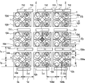
图1是示出根据本发明第一实施例的固态成像器件的示意性配置的平面图。如图1所示,该固态成像器件由以矩阵形式布置的多个像素构成,即,行和列形式的像素矩形阵列。例如,图1示出围绕成像器件的中心C的36个像素(每列6个像素×每行6个像素)。FIG. 1 is a plan view showing a schematic configuration of a solid-state imaging device according to a first embodiment of the present invention. As shown in FIG. 1, the solid-state imaging device is composed of a plurality of pixels arranged in a matrix, that is, a rectangular array of pixels in the form of rows and columns. For example, FIG. 1 shows 36 pixels (6 pixels per column x 6 pixels per row) surrounding the center C of the imaging device.
下文,标号1指光接收单元,标号2指传输栅。而且,标号103指第一光波导,标号104指第二光波导,标号105指片上透镜。标号10指半导体基板,标号11指电荷累积层,标号12指正电荷累积区域,标号13指栅绝缘膜,标号14指栅电极。此外,标号18、23和28指阻隔金属层,标号19、24和29指导电层。标号20指第一防扩散膜,标号32和37指埋入层,标号36指钝化膜,标号38指平面化树脂层,标号39指颜色过滤器。标号100指信号线路,标号110指布线线路。标号500指成像装置,标号501指成像单元,标号502指光学系统,标号503指信号处理器。在图中,“FD”表示浮置扩散区,“RST”表示复位晶体管,“Amp”表示放大晶体管,“SEL”表示选择晶体管。Hereinafter,
每个像素具有包括光接收单元1、第一光波导103、第二光波导104和片上透镜105的光电二极管。光接收单元1对接收的光执行光电转换。第一光波导103和第二光波导104将入射光引入光接收单元1。片上透镜105使入射光汇聚。第一和第二光波导103和104中的每个具有圆形截面形状。第一光波导103位于下侧作为下层(在光接收单元1那侧)。第二光波导104位于上侧作为上层(在片上透镜105那侧)。上层第二光波导104的开口直径小于下层第一光波导103的开口直径。Each pixel has a photodiode including a
总共四个像素(列上两个×行上两个)共享浮置扩散区FD,该浮置扩散区FD可以累积光学转换所产生的电荷。在四个像素中的每一个中,在光接收单元1和由四个像素共享的浮置扩散区FD之间形成传输栅2。A total of four pixels (two on the column×two on the row) share the floating diffusion FD which can accumulate charges generated by optical conversion. In each of the four pixels, a
另外,在具有共享的浮置扩散区FD的四个像素的上侧和下侧布置了晶体管Tr1、Tr2和Tr3。各个晶体管Tr1、Tr2和Tr3的示例性配置包括(但不局限于)放大晶体管、复位晶体管和选择晶体管。In addition, transistors Tr1 , Tr2 , and Tr3 are arranged on the upper and lower sides of the four pixels having the shared floating diffusion region FD. Exemplary configurations of the respective transistors Tr1, Tr2, and Tr3 include, but are not limited to, amplification transistors, reset transistors, and selection transistors.
图2示出位于图1右下方的四个像素。FIG. 2 shows the four pixels located at the bottom right of FIG. 1 .
在本实施例的固态成像器件中,共享浮置扩散区FD的四个像素作为一基本单元而提供。在图2中,在图1的右下方的基本单元和成像器件的中心C被示出。In the solid-state imaging device of the present embodiment, four pixels sharing the floating diffusion FD are provided as a basic unit. In FIG. 2 , the base unit and the center C of the imaging device at the lower right of FIG. 1 are shown.
如图2所示,在四个像素中的每一个中,第一光波导103的中心(未示出)和第二光波导104的中心104C两者都相对光接收单元1的中心C被移位。As shown in FIG. 2, in each of the four pixels, both the center (not shown) of the first
具体讲,在图中的两个上侧像素中,第一光波导103的中心(未示出)和第二光波导104的中心104C两者都相对光接收单元1的中心1C被向上移位。在图中的两个下侧像素中,第一光波导103的中心(未示出)和第二光波导104的中心104C两者都相对光接收单元1的中心1C被向下移位。这里,考虑从成像器件的中心C画到每个像素的光接收单元1的中心1C的线段。在两个上侧像素的情况下,从成像器件的中心C到第一光波导103的中心以及第二光波导104的中心104C两者的距离比距光接收单元1的中心1C的距离短。相反,在两个下侧像素的情况下,从成像器件的中心C到第一光波导103的中心以及第二光波导104的中心104C两者的距离比距光接收单元1的中心1C的距离长。换言之,基本单元包括两种不同像素的混合,一种是使得从成像器件的中心C到第一光波导103的中心以及第二光波导104的中心104C两者的距离比距光接收单元1的中心1C的距离短,另一种是使得成像器件的中心C到第一光波导103的中心以及第二光波导104的中心104C两者的距离比距光接收单元1的中心1C的距离长。Specifically, in the two upper pixels in the figure, both the center (not shown) of the first
返回图1(完整像素的平面图),也存在两种不同像素的混合,一种是使得从成像器件的中心C到第一光波导103的中心以及第二光波导104的中心104C两者的距离比距光接收单元1的中心1C的距离短,另一种是使得成像器件的中心C到第一光波导103的中心以及第二光波导104的中心104C两者的距离比距光接收单元1的中心1C的距离长。使得从成像器件的中心C到第一光波导103的中心以及第二光波导104的中心104C两者的距离比距光接收单元1的中心1C的距离短的像素是图中从上侧起第二行的像素和从下侧起第二行的像素。在其余四行的像素中,从成像器件的中心C到第一光波导103的中心以及第二光波导104的中心104C两者的距离比距光接收单元1的中心1C的距离长。Returning to FIG. 1 (the plan view of a complete pixel), there are also two kinds of different pixel mixtures, one is to make the distance from the center C of the imaging device to the center of the first
另一方面,在日本专利早期公开No.2006-261247所描述的成像器件中,所有像素都是使得从成像器件的中心C到第一光波导103的中心以及第二光波导104的中心104C两者的距离等于或小于距光接收单元1的中心1C的距离的像素。除此之外,不存在使得使得从成像器件的中心C到第一光波导103的中心以及第二光波导104的中心104C两者的距离比距光接收单元1的中心1C的距离长的像素。因此,本实施例的成像器件的配置完全不同于通常的成像器件。On the other hand, in the imaging device described in Japanese Patent Laid-Open Publication No. 2006-261247, all the pixels are such that from the center C of the imaging device to the
图3到图5中的每张图是图1所示固态成像器件的某些组件的平面图。具体讲,图3示出第一光波导103、第二光波导104、光接收单元1、晶体管Tr1、Tr2和Tr3等等。图4只示出片上透镜105。图5表示片上透镜105、第一光波导103和第二光波导104。在图3到图5中,成像器件的中心C也与这些组件一起被表示出。Each of FIGS. 3 to 5 is a plan view of some components of the solid-state imaging device shown in FIG. 1 . Specifically, FIG. 3 shows the first
如图3所示,各个像素的光接收单元1被规则地布置以使得四个像素构成一个基本单元。As shown in FIG. 3 , the
基本单元的四个像素是以共享的浮置扩散区FD为共同的中心而布置在其周围的。The four pixels of the basic unit are arranged around the common center of the shared floating diffusion FD.
另一方面,这些像素中的上侧两个像素和下侧两个像素彼此间隔开并中间夹入晶体管Tr1、Tr2和Tr3。另外,像素之间的空间隔行改变。换言之,在行方向上,隔着晶体管而相邻的基本单元的像素之间的距离1c大于同一基本单元中的像素之间的距离1a。On the other hand, of these pixels, the upper two pixels and the lower two pixels are spaced apart from each other with the transistors Tr1 , Tr2 , and Tr3 interposed therebetween. In addition, the space between pixels changes alternately. In other words, in the row direction, the
而且,在列方向上,相邻基本单元的像素之间的距离大于同一基本单元中的像素之间的距离。此外,像素之间的距离隔列改变。就是说,相邻基本单元的像素之间的距离1d大于同一基本单元中的像素之间的距离。Also, in the column direction, the distance between pixels of adjacent basic units is greater than the distance between pixels in the same basic unit. In addition, the distance between pixels changes every column. That is, the
下文,在列方向上同一基本单元的第一光波导103之间的距离被定义为波导距离103a。在列方向上相邻基本单元的第一光波导103之间的距离被定义为波导距离103c。在行方向上,同一基本单元的第一光波导103之间的距离被定义为波导距离103b,而相邻基本单元的第一光波导103之间的距离被定义为波导距离103d。类似地,在列方向上同一基本单元的第二光波导104之间的距离被定义为波导距离104a。在列方向上相邻基本单元的第二光波导104之间的距离被定义为波导距离104c。在行方向上,同一基本单元的第二光波导104之间的距离被定义为波导距离104b,而相邻基本单元的第二光波导104之间的距离被定义为波导距离104d。Hereinafter, the distance between the first
在列方向上,第一光波导103之间的距离隔行改变。换言之,同一基本单元的第一光波导103之间的距离103a不同于中间夹入晶体管的相邻基本单元的第一光波导103之间的距离103c。另外,在行方向上第一光波导103之间的距离隔列稍微改变。在行方向上,同一基本单元的第一光波导103之间的距离103b不同于中间夹入晶体管的相邻基本单元的第一光波导103之间的距离103d。In the column direction, the distance between the first
相反,第二光波导104在列方向上被布置得基本等距。就是说,在列方向上,同一基本单元中的第二光波导104之间的距离104a几乎等于中间夹入晶体管的相邻基本单元的第二光波导104之间的距离104c。另外,在行方向上第二光波导104之间的距离隔列稍微改变。在行方向上,同一基本单元的第二光波导104之间的距离104b稍微不同于中间夹入晶体管的相邻基本单元的第二光波导104之间的距离104d。此外,在每个像素中,光接收单元1之内包含第一和第二光波导103和104的该平面配置。In contrast, the second
此外,在同一平面中看去,下侧的第一光波导103中包含上侧的第二光波导104。Also, when viewed on the same plane, the lower first
如图4所示,片上透镜105在列方向上和行方向上以基本等间距布置。就是说,在列方向上,同一基本单元的片上透镜105之间的距离基本等于中间夹入晶体管的相邻基本单元的透镜105之间的距离。因此,这些距离用同一标号105a表示。另外,在行方向上,同一基本单元的片上透镜105之间的距离基本等于中间夹入晶体管的相邻基本单元的透镜105之间的距离。因此,这些距离用同一标号105b表示。As shown in FIG. 4 , the on-
如果片上透镜105之间的这些距离不相等,那么当各个像素的片上透镜以相同的直径和相同的曲率被准备时,会在片上透镜之间的具有相对较宽距离的部分中扩展出没有汇聚的入射光的区域,或称无效区。If these distances between the on-
如图5所示,第一和第二光波导103和104与片上透镜105之间的相对位置取决于像素的位置而变化。As shown in FIG. 5, the relative position between the first and second
在上侧两行的每个像素中,从成像器件的中心C观看,第一光波导103被移位到片上透镜105的上部,并且第二光波导104位于片上透镜105的上半部分。在成像器件的中心C的相反两侧的两行中的每个像素中,第一光波导103和第二光波导104两者都在列方向上位于片上透镜105的中心附近。In each pixel of the upper two rows, viewed from the center C of the imaging device, the first
在下侧两行的每个像素中,从成像器件的中心C观看,第一光波导103被移位到片上透镜105的下部,并且第二光波导104位于片上透镜105的下半部分。In each pixel of the lower two rows, viewed from the center C of the imaging device, the first
在右侧两列的每个像素中,从成像器件的中心C观看,第一光波导103被移位到片上透镜105的右部,并且第二光波导104位于片上透镜105的右半部分。In each pixel of the right two columns, the first
在成像器件的中心C的相反两侧的两列中的每个像素中,第一光波导103和第二光波导104两者都在行方向上位于片上透镜105的中心附近。在左侧两列的每个像素中,从成像器件的中心C观看,第一光波导103被移位到片上透镜105的左部,并且第二光波导104位于片上透镜105的左半部分。In each pixel in two columns on opposite sides of the center C of the imaging device, both the first
此外,在每个像素中,第二光波导104的平面配置被包括在光接收单元1之内。Furthermore, in each pixel, the planar configuration of the second
另一方面,各个像素的某些第一光波导103部分地在相应片上透镜105外部。On the other hand, some of the first
在该第一实施例中,片上透镜105和光接收单元1之间的相对位置取决于从成像器件的中心观看的像素的位置而变化。另外,片上透镜105取决于从成像器件的中心C到像素的距离而被从光接收单元的中心1C向成像器件的中心C移位。In this first embodiment, the relative position between the on-
就是说,片上透镜105已通过光瞳校正被处理。这里,术语“光瞳校正”指波导相对于片上透镜或光接收单元被移位到适当位置上,来针对下述情况采取措施:入射光不是垂直入射而是倾斜入射到像素外围。另一方面,第一光波导103和第二光波导104两者都没有被光瞳校正所处理。That is, the on-
此外,组件之间的距离如下:在同一基本单元的上下两侧的两个像素的情况下,光波导之间的距离103a大于像素之间的距离1a。在同一基本单元的左右两侧的两个像素的情况下,光波导之间的距离103b稍大于像素之间的距离1b。In addition, the distance between components is as follows: In the case of two pixels on the upper and lower sides of the same basic unit, the
在同一基本单元的上下两侧的两个像素之间的距离1a不同于中间夹入晶体管的相邻基本单元的像素之间的距离1c。The
波导距离103a和波导距离103c彼此基本相等。此外,虽然优选地波导距离103a和波导距离103c彼此基本相等,但是波导距离103a和波导距离103c也可以彼此不相等。The
如果光波导之间的距离以等间距布置,则行方向上的第一光波导103的入射角度依赖性的增大,并且可以改善导致某些现象(例如水平条纹和暗影,horizontal stripes and shading)的光学属性。If the distances between the optical waveguides are arranged at equal intervals, the incident angle dependence of the first
波导距离103b和波导距离103d彼此稍有不同。波导距离103d稍大于波导距离103b。优选的,波导距离103b等于波导距离3d,但并不局限于相等。The
与同一基本单元的左右两侧的两个像素之间的距离1b相比,在行方向上的相邻基本单元的像素之间的距离1d稍长。顺便提及,像素之间的距离1b和像素之间的距离1d可以基本相等。The
波导距离103b和波导距离103d之间的差置基本等于像素距离1b和像素距离1d之间的差值。因此,第一光波导103的中心位于光接收单元1的中心1C附近。The difference between the
在同一基本单元的上下两侧的两个像素的情况下,光波导之间的距离104a大于像素之间的距离1a。In the case of two pixels on the upper and lower sides of the same basic unit, the
这里,波导距离104a可以等于或大于像素距离1a。Here, the
波导距离104c大于波导距离104a。The
波导距离104b和波导距离104d彼此稍有不同。波导距离104d稍大。The
像素距离1a和像素距离1c之和等于波导距离103a和波导距离103c之和,也等于波导距离104a和波导距离104c之和。这些和等同于列方向上的基本单元之间的节距(pitch)。The sum of the
像素距离1b和像素距离1d之和等于波导距离103b和波导距离103d之和,也等于波导距离104b和波导距离104d之和。这些和等同于行方向上的基本单元之间的节距。The sum of the
每个像素的截面配置不受具体限制,只要其包括光接收单元1、第一光波导103、第二光波导104和片上透镜105即可。The cross-sectional configuration of each pixel is not particularly limited as long as it includes the
图6是图1所示固态成像器件的像素的示例性配置的截面图。6 is a cross-sectional view of an exemplary configuration of a pixel of the solid-state imaging device shown in FIG. 1 .
如图6所示,光接收单元1是通过在半导体基板10的p阱区域(p-well region)等上形成n型电荷累积层11并在n型电荷累积层11的表面上形成p+型正电荷累积层12来构造的。As shown in FIG. 6 , the light-receiving
此外,栅绝缘膜13和栅电极14被形成在半导体基板10上,同时与光接收单元1的右侧相邻。栅电极14是图1中的传输栅。浮置扩散区FD形成在半导体基板10中,同时与栅电极14的右侧相邻。在半导体基板10的截面(未示出)中,形成晶体管Tr1、Tr2和Tr3的源/漏区域。施加到栅电极14的电压造成信号电荷从光接收单元1到浮置扩散区FD的传输。Furthermore, a
由氧化硅等构成的绝缘膜被层压(laminate)在半导体基板10上,同时覆盖光接收单元1。绝缘膜包括第一绝缘膜15、第二绝缘膜16、第三绝缘膜17、第四绝缘膜21、第五绝缘膜22、第六绝缘膜26、第七绝缘膜27和第八绝缘膜31。另外,由碳化硅等构成的第一防扩散膜20和第二防扩散膜25以及由氮化硅的构成的第三防扩散膜30被分别层压在绝缘膜之间。这些绝缘膜和防扩散膜的层压使得绝缘层成为一整体。An insulating film composed of silicon oxide or the like is laminated on the
在第三绝缘膜17中形成布线沟槽,并且由阻隔金属层18和导电层19构成的第一布线层随后被埋入该布线沟槽中。同样,在第五绝缘膜22中形成布线沟槽,并且由阻隔金属层23和导电层24构成的第二布线层随后被埋入该布线沟槽中。同样,在第七绝缘膜27中形成布线沟槽,并且由阻隔金属层28和导电层29构成的第三布线层随后被埋入该布线沟槽中。阻隔金属层18、23和28中的每一个例如可以是钽/氮化钽的叠层膜。导电层19、24和29中的每一个例如可以是用于布线线路的各种金属性材料中的任意一种,例如铜。上述第一到第三防扩散膜被提供以防止导电层19、24和29的诸如铜之类的金属分散开。A wiring trench is formed in the third insulating
由氧化硅构成的第九绝缘膜33被形成在第八绝缘膜31上。A ninth insulating
此外,埋入层32被埋入在光接收单元1之上的第二绝缘膜16和第三绝缘膜17中,以使其穿过这些膜16和17。埋入层32具有比绝缘膜的氧化硅的折射率(折射率为1.45)更高的折射率。埋入层32构成下侧的第一光波导103。Furthermore, the buried layer 32 is buried in the second insulating
此外,在光接收单元1之上形成有凹陷部分,以使其穿过如上所述层压而成的第四到第九绝缘膜21到33和第二和第三防扩散膜25和30。第一防扩散膜20被形成在该凹陷部分的底部上。Further, a depressed portion is formed over the
该凹陷部分的内壁表面垂直于基板的主平面。第九绝缘膜33的一部分被提供作为凹陷部分的边缘,并且以向前变尖的形状形成一向上变宽的开口。The inner wall surface of the concave portion is perpendicular to the main plane of the substrate. A part of the ninth insulating
钝化膜36被形成以使其覆盖凹陷部分的内壁表面。另外,例如,埋入层37被形成在钝化膜36上并埋入到凹陷部分中。埋入层37具有比绝缘膜的氧化硅的折射率(折射率为1.45)更高的折射率。埋入层37完全填满凹陷部分的内部。The
埋入层32和埋入层37中的每个可以由具有高折射率的树脂构成,例如硅氧烷树脂(折射率1.7)或聚酰亚胺。为了增大折射率,这些树脂材料可以包含任意金属氧化物粒子,包括氧化钛、氧化钽、氧化铌、氧化钨、氧化锆、氧化锌、氧化铟和氧化铪。任意具有高折射率的无机材料都可以被使用,只要其可以被埋入凹陷部分的内部即可。Each of the embedding layer 32 and the embedding
埋入层32和埋入层37可以分别由不同的材料构成。The embedding layer 32 and the embedding
钝化膜36可以用与用作绝缘膜的氧化硅具有相等或接近的折射率的材料或具有高于氧化硅的折射率的材料构成。具有较高折射率的材料的示例包括氮化硅和氧氮化硅(SiON)。The
如果钝化膜36由与用作绝缘膜的氧化硅具有相等或接近的折射率的材料构成,则在凹陷部分的内部的埋入层37充当上侧的第二光波导104。If the
如果钝化膜36由具有高于用作绝缘膜的氧化硅的折射率的材料构成,则在上侧的第二光波导104由凹陷部分内部的钝化膜36和埋入层37构成。If
平面化树脂层38(其还可以充当接合层)被形成在埋入层37上。因此,例如,每个像素具有蓝色(B)、绿色(G)和红色(R)颜色过滤器39之一。此外,片上透镜105被形成在颜色过滤器39上。A planarizing resin layer 38 (which may also serve as a bonding layer) is formed on the buried
从图6显而易见,第一光波导103的宽度稍小于光接收单元1的宽度。另外,第一光波导103被形成为使其在该固态成像器件的表面中的位置可以在该固态成像器件的表面中位于光接收单元1的位置以内。As apparent from FIG. 6 , the width of the first
另外,第二光波导104的宽度稍小于光接收单元1的宽度和第一光波导103的宽度。另外,第二光波导104被形成为使其在该固态成像器件的表面中的位置可以在该固态成像器件的表面中位于光接收单元1、第一光波导103和片上透镜105中每一个的位置以内。In addition, the width of the second
基于图6所示的像素结构,像素被形成为使得光接收单元1、第一光波导103、第二光波导104和片上透镜105中的每一个在该固态成像器件的表面中的位置相对于像素距成像器件的中心C的位置被移位。Based on the pixel structure shown in FIG. 6, the pixel is formed such that the position of each of the
例如,具有图6所示像素的截面结构的固态成像器件可以按如下方式制造:For example, a solid-state imaging device having a cross-sectional structure of a pixel shown in FIG. 6 can be fabricated as follows:
n型电荷累积层11被形成在半导体基板10的p阱区域等上,并且p+型正电荷累积层12随后被形成在n型电荷累积层11的表面上以提供光接收单元1。另外,栅绝缘膜13和栅电极14被形成在半导体基板10上,同时与光接收单元1相邻。此外,浮置扩散区FD以及晶体管Tr1、Tr2和Tr3的源/漏区域被形成在半导体基板10中。N-type
接下来,例如,光接收单元1被利用化学气相沉积(CVD)方法等沉积在光接收单元1的整个表面上的氧化硅所覆盖,以形成第一绝缘膜15。随后,例如,氧化硅被沉积在第一绝缘膜15上以形成第二绝缘膜16,并且在其上进一步沉积氧化硅以形成第三绝缘膜17。Next, for example, the
接下来,例如,第三绝缘膜17受到蚀刻处理以形成布线线路沟槽。布线沟槽的内壁通过溅射被例如钽/氧化钽所覆盖以形成阻隔金属层18。Next, for example, the third insulating
此后,铜种子层(seed layer)被形成并受到电镀,从而在此前的结构的整个表面上形成铜膜。然后,所形成的膜受到化学机械抛光(CMP)等以去除布线沟槽外部的铜膜,从而形成导电层19。Thereafter, a copper seed layer is formed and subjected to electroplating, thereby forming a copper film on the entire surface of the previous structure. Then, the formed film is subjected to chemical mechanical polishing (CMP) or the like to remove the copper film outside the wiring trench, thereby forming the
此外,阻隔金属层18被形成在导电层19的表面上,并且其形成在布线沟槽外部的部分随后被去除。在图6中,阻隔金属层18也形成在导电层19的表面上。但是,如果不希望将阻隔金属层18形成在导电层19的表面上,则省略该步骤。In addition, a
因此,由埋入布线沟槽的阻隔金属层18和导电层19构成的第一布线层被形成。Thus, a first wiring layer composed of the
随后,第二绝缘膜16和第三绝缘膜17都被蚀刻以形成穿过这些膜16和17的开口。Subsequently, both the second insulating
然后,例如,在大约400℃的沉积温度下,通过旋涂方法、利用包含氧化钛等的金属氧化物粒子的硅氧烷树脂来形成膜以填充在孔中。因此,形成埋入层32,其具有比氧化硅更高的折射率。在涂敷了树脂之后,例如,如果需要,在大约300℃的温度下执行烘烤后处理(post-bakingprocessing)。在聚酰胺树脂的情况下,例如,可以在大约350℃的温度下执行膜的形成。Then, for example, at a deposition temperature of about 400° C., a film is formed to fill in the pores by a spin coating method using a silicone resin containing metal oxide particles of titanium oxide or the like. Thus, the buried layer 32 is formed, which has a higher refractive index than silicon oxide. After the resin is applied, for example, post-baking processing is performed at a temperature of about 300° C., if necessary. In the case of polyamide resin, for example, film formation can be performed at a temperature of about 350°C.
接下来,例如,通过CVD方法等在第一布线层上沉积碳化硅,以形成第一防扩散膜20。Next, for example, silicon carbide is deposited on the first wiring layer by a CVD method or the like to form first
随后,执行以与形成第二绝缘膜16、第三绝缘膜17及其布线沟槽、由阻隔金属层18和导电层19构成的第一布线层和第一防扩散膜20相同的过程。从而,这些过程形成第四绝缘膜21、第五绝缘膜22及其布线沟槽、由阻隔金属层23和导电层24构成的第二布线层、第二防扩散膜25、第六绝缘膜26、第七绝缘膜27及其布线沟槽、以及由阻隔金属层28和导电层29构成的第三布线层。此外,例如,通过CVD方法沉积氮化硅以形成第三防扩散膜30。接下来,第八绝缘膜31被形成在第三防扩散膜30上。Subsequently, the same process as that for forming the second insulating
此后,例如,在第八绝缘膜31的整个表面上沉积氧化硅以形成第九绝缘膜33。Thereafter, for example, silicon oxide is deposited on the entire surface of the eighth insulating
随后,例如,通过光刻工艺对一抗蚀膜进行凹陷部分开口的图案形成,然后对该抗蚀膜进行各向同性蚀刻或各向异性蚀刻。结果,在第九绝缘膜33中形成以向前变尖的形状向上变宽的开口。Subsequently, for example, a resist film is subjected to patterning of recessed portion openings by a photolithography process, and then the resist film is subjected to isotropic etching or anisotropic etching. As a result, an opening that widens upward in a forwardly tapered shape is formed in the ninth insulating
接下来,该抗蚀膜被去除,并例如随后用与第一抗蚀膜相同的图案对第二抗蚀膜进行图案化。经过图案化的第二抗蚀膜受到各向异性蚀刻(例如反应离子蚀刻)来形成穿过第四到第九绝缘膜21到33、第二防扩散膜25和第三防扩散膜30的凹陷部分。在形成该凹陷部分期间,例如,在随氮化硅、碳化硅等以及氧化硅的材料而改变条件的同时进行蚀刻。当开口的底部到达第一防扩散膜20时蚀刻立即停止。结果,第一防扩散膜20充当凹陷部分的底部。因此,凹陷部分的恒定深度使得光接收单元1和第二光波导104之间的距离恒定。Next, this resist film is removed, and then, for example, the second resist film is patterned with the same pattern as the first resist film. The patterned second resist film is subjected to anisotropic etching (such as reactive ion etching) to form recesses through the fourth to ninth insulating
这样,第九绝缘膜33的一部分被提供作为凹陷部分的边缘并且以向前变尖的形状形成开口。In this way, a part of the ninth insulating
接下来,例如,在大约380℃的沉积温度下、通过等离子CVD方法将具有高于氧化硅的折射率的氮化硅或氧氮化硅(SiON)沉积在凹陷部分的内壁上以形成钝化膜36。由于开口的边缘是以向前变尖的形状形成的,因此钝化膜36的轮廓被形成为如下:由于沉积的各向异性,其轮廓在开口的边缘处形成得较厚,而在凹陷部分的底部附近形成得较薄。Next, for example, silicon nitride or silicon oxynitride (SiON) having a higher refractive index than silicon oxide is deposited on the inner wall of the recessed portion by a plasma CVD method at a deposition temperature of about 380° C. to form a passivation film36. Since the edge of the opening is formed in a shape that tapers forward, the profile of the
接下来,例如,在大约400℃的沉积温度下,通过旋涂方法用包含诸如氧化钛之类的金属氧化物粒子的硅氧烷树脂来覆盖钝化膜36。因此,具有比氧化硅更高的折射率的埋入层37被布置在钝化膜36的顶部并被埋入在凹陷部分中。Next, the
在涂敷树脂之后,例如,如果需要,在大约300℃的温度下执行烘烤后处理。在聚酰胺树脂的情况下,例如,可以在大约350℃的温度下执行膜的形成。After coating the resin, for example, post-bake treatment is performed at a temperature of about 300° C., if necessary. In the case of polyamide resin, for example, film formation can be performed at a temperature of about 350°C.
接下来,例如,在埋入层37的顶部形成平面化树脂层38。平面化树脂层38也可以充当接合层。在平面化树脂层38的顶部,例如,针对每个像素设置蓝色(B)、绿色(G)和红色(R)中的各种的颜色过滤器39。随后,在颜色过滤器39的顶部形成片上透镜105。Next, for example, a
在上述制造方法中,在形成第三布线层的步骤之后、但在形成埋入层的步骤之前,可以执行加氢处置(hydrogen disposal)(烧结)以用于封端(terminate)半导体中的悬空键(dangling bond)。In the above manufacturing method, after the step of forming the third wiring layer but before the step of forming the buried layer, hydrogen disposal (sintering) may be performed for terminating the vacancy in the semiconductor. key (dangling bond).
因此,具有图6所示像素的截面结构的固态成像器件可以被制造。Therefore, a solid-state imaging device having the cross-sectional structure of the pixel shown in FIG. 6 can be manufactured.
然后,图7示意性地示出像素的平面布局。Then, FIG. 7 schematically shows a planar layout of pixels.
在该图中,第一光波导103截面呈圆形,在第一光波导103中形成具有圆形截面的第二光波导104。布线层(例如图6中的第一到第三布线层)被形成以使得它们在绝缘膜中围绕第一光波导103呈网格结构布置。术语“网格结构”指例如布线层和绝缘膜在列方向上被交替堆叠。In this figure, a first
例如,在图7中,第一光波导103和第二光波导104都被布置在由在列方向上延伸的布线层W1和W2和在水平方向上延伸的布线层W3和W4所围绕的区域中。布线层W1、W2、W3和W4可以具有它们自己的网格结构。For example, in FIG. 7, both the first
虽然光接收单元1没有表示在图7中,但是光接收单元1被形成在比第一光波导103更外侧。例如,在图6所示截面结构的情况下,光接收单元1的外边缘位于布线层W1、W2、W3和W4的位置附近。Although the
现在参考图8,将描述图1所示的36个像素上的颜色过滤器的颜色的示例性布置。Referring now to FIG. 8 , an exemplary arrangement of colors of the color filters on the 36 pixels shown in FIG. 1 will be described.
在图8所示的颜色布置中,一个红色(R)、一个蓝色(B)和两个绿色(G:Gb和Gr)颜色过滤器被分配给每个基本单元的四个像素中的每一个。然后,绿色(Gb)和绿色(Gr)被分配给隔着浮置扩散区FD而彼此相对的像素。而且,红色(R)和蓝色(B)被分配给隔着浮置扩散区FD而彼此相对的像素。In the color arrangement shown in Figure 8, one red (R), one blue (B) and two green (G: Gb and Gr) color filters are assigned to each of the four pixels of each basic unit one. Then, green (Gb) and green (Gr) are assigned to pixels facing each other across the floating diffusion FD. Also, red (R) and blue (B) are assigned to pixels facing each other across the floating diffusion FD.
图9是示出根据本发明第一实施例的固态成像器件中的基本单元的四个像素的示例性等效电路的图。9 is a diagram showing an exemplary equivalent circuit of four pixels of a basic unit in the solid-state imaging device according to the first embodiment of the present invention.
如图9所示,由四个光电二极管构成的光接收单元1通过传输栅2被连接到公共的浮置扩散区FD。另外,浮置扩散区FD被连接到复位晶体管RST的源/漏区域之一以及放大晶体管Amp的栅极。As shown in FIG. 9 , a
放大晶体管Amp的源/漏区域之一被连接到选择晶体管SEL的源/漏区域之一。复位晶体管RST的源/漏区域中的另一个和放大晶体管Amp的源/漏区域中的另一个被连接到电源电势Vdd。选择晶体管SEL的源/漏区域中的另一个被连接到信号线路100。换言之,三个晶体管RST、Amp和SEL的来自浮置扩散区FD那侧的部分具有与具有四个晶体管(包括晶体管栅极的传输晶体管)的典型像素相同的配置。One of the source/drain regions of the amplification transistor Amp is connected to one of the source/drain regions of the selection transistor SEL. The other of the source/drain regions of the reset transistor RST and the other of the source/drain regions of the amplification transistor Amp are connected to the power supply potential Vdd. The other of the source/drain regions of the selection transistor SEL is connected to the
现在参考图10,将描述实现了图9所示的电路配置的两个示例。Referring now to FIG. 10 , two examples implementing the circuit configuration shown in FIG. 9 will be described.
图10是示出由基本单元的四个像素所使用的晶体管之间的位置关系的图。多个带状晶体管Tr被分别布置在具有四个像素的基本单元的上侧和下侧。FIG. 10 is a diagram showing a positional relationship between transistors used by four pixels of a basic unit. A plurality of strip transistors Tr are respectively arranged on the upper side and the lower side of a basic unit having four pixels.
在第一示例中,如图10中的点划线所表示的,上侧晶体管Tr的右半部分和下侧晶体管Tr的右半部分被使用。各个晶体管的左半部分被位于这些晶体管的上面和下面的各个基本单元的四个像素所使用。In the first example, the right half of the upper side transistor Tr and the right half of the lower side transistor Tr are used as indicated by the chain line in FIG. 10 . The left half of each transistor is used by the four pixels of each basic unit above and below these transistors.
在第二示例中,如图10中的虚线所表示的,整个下侧晶体管被使用。上侧晶体管被位于该晶体管上面的基本单元的四个像素所使用。In the second example, as indicated by the dotted line in Fig. 10, the entire lower side transistor is used. The upper side transistor is used by the four pixels of the basic unit above the transistor.
在第一示例中的布线示例如图11A所示。复位晶体管RST被形成在上侧晶体管Tr的右半部分上。相反,放大晶体管Amp和选择晶体管SEL被形成在下侧晶体管Tr的右半部分上。信号线路100被形成为使其从下侧纵向延伸到上侧,以将浮置扩散区FD连接到复位晶体管RST的源/漏区域之一以及放大晶体管Amp的栅极。An example of wiring in the first example is shown in Fig. 11A. The reset transistor RST is formed on the right half of the upper side transistor Tr. In contrast, the amplification transistor Amp and the selection transistor SEL are formed on the right half of the lower side transistor Tr. The
在第二示例中的布线示例如图11B所示。复位晶体管RST被形成在下侧晶体管Tr的右半部分上。放大晶体管Amp被形成在下侧晶体管Tr的中间。选择晶体管SEL被形成在下侧晶体管Tr的左半部分上。浮置扩散区FD和放大晶体管Amp的栅极通过在下侧纵向延伸的布线线路110相连。布线线路110从其中途点向右分支并随后被连接到复位晶体管RST的源/漏区域之一。An example of wiring in the second example is shown in Fig. 11B. The reset transistor RST is formed on the right half of the lower side transistor Tr. The amplification transistor Amp is formed in the middle of the lower side transistor Tr. The selection transistor SEL is formed on the left half of the lower side transistor Tr. The floating diffusion FD and the gate of the amplification transistor Amp are connected through a
根据以上实施例,基本单元的四个像素共享浮置扩散区FD和晶体管Tr1、Tr2和Tr3。因此,与浮置扩散区FD和晶体管Tr1、Tr2和Tr3没有被共享的情况相比,可以增大光接收单元1的表面积占像素的表面积的比例,或者可以扩大光接收单元1的表面积。可以减轻使像素小型化时光接收单元1面积的减小。因此,有可能使像素极大地小型化至可能情况的最小,同时防止第一和第二光波导103和104的尺寸成为埋入属性的限制。According to the above embodiment, four pixels of a basic unit share the floating diffusion FD and the transistors Tr1, Tr2, and Tr3. Therefore, the ratio of the surface area of the
因此,有可能使像素小型化以有助于固态成像器件的集成。而且,有可能提供具有包含更多像素的固态成像器件的成像装置,并使该成像装置小型化。Therefore, it is possible to miniaturize pixels to facilitate integration of solid-state imaging devices. Also, it is possible to provide an imaging device having a solid-state imaging device including more pixels and to miniaturize the imaging device.
根据本实施例,片上透镜105是等间距形成的。因此,可以减小所谓的无效区并且可以防止由于无效区而导致损耗的生成。According to the present embodiment, the on-
另外,第二光波导104的平面位置被形成为使得其可以从光接收单元1的中心1C向晶体管Tr1、Tr2和Tr3移位。此外,其还被形成为使其能够被包括在第一光波导103之内以及片上透镜105之内。因此,由片上透镜105所收集的光可以被完全引导至第二光波导104,并且穿过第二光波导104的光随后可以确保入射到第一光波导103上。这样,第二光波导104在固态成像器件的表面中的位置被包括在第一光波导103之内。因此,在日本专利早期公开No.2006-261247中所描述的器件的配置中没有进入下侧光波导的光可以进入。In addition, the planar position of the second
此外,第一光波导103的平面位置被形成为使其可以从光接收单元1的中心1C向晶体管Tr1、Tr2和Tr3移位。此外,其还被形成为使其能够被包括在光接收单元1的第一光波导103的内部。Furthermore, the planar position of the first
因此,穿过第二光波导104的光可以确保入射到光接收单元1上。另外,可以防止在穿过第一光波导103的光进入相邻像素的光接收单元1时发生混合颜色的生成。Therefore, the light passing through the second
因此,可以实现灵敏度的增大和光电转换效率的增大。因此,即使像素被小型化,也能够实现具有足够的灵敏度和足够的光电转换效率的固态成像器件。而且,可以实现具有这种固态成像器件的成像装置。Therefore, an increase in sensitivity and an increase in photoelectric conversion efficiency can be achieved. Therefore, even if the pixel is miniaturized, a solid-state imaging device having sufficient sensitivity and sufficient photoelectric conversion efficiency can be realized. Also, an imaging apparatus having such a solid-state imaging device can be realized.
此外,根据本实施例,成像器件具有两层光波导,即第一光波导103和第二光波导104。因此,与具有上层光波导的器件相比,可以避免颜色混合和损耗。相对于光接收单元1的中心1C的移位量可以被分担。因此,可以扩展设计光波导的灵活性。另外,还可以应对片上透镜105相对光接收单元1的相对较大的移位量。Furthermore, according to the present embodiment, the imaging device has two layers of optical waveguides, that is, the first
此外,根据本发明,第二光波导104是以几乎等间距布置的,从而可以改善导致某些现象(例如,水平条纹、不规则颜色和暗影)的光学属性。Furthermore, according to the present invention, the second
在第一实施例中,各组件被布置为使得:距成像器件的中心C的距离向外增大得越多,则从片上透镜105的中心到第一和第二光波导103和104的中心中每一个的距离增大得越多。具有这种配置的成像器件优选地被用于具有短焦光学镜头的相机(例如,蜂窝电话相机)。In the first embodiment, the components are arranged such that: the more outwardly the distance from the center C of the imaging device increases, the more the distance from the center of the on-
在以上描述中,根据本发明第一实施例的示例性固态成像器件包括36个像素,如图1所示。但是,本实施例并不局限于固态成像器件的这种配置。在实践中,固态成像器件可以包括上万个或更多的像素。In the above description, the exemplary solid-state imaging device according to the first embodiment of the present invention includes 36 pixels, as shown in FIG. 1 . However, the present embodiment is not limited to this configuration of the solid-state imaging device. In practice, solid-state imaging devices may include tens of thousands or more pixels.
例如,通过累积750,000个基本单元可以获得总共三百万个像素(每个单元四个像素)。For example, a total of three million pixels (four pixels per cell) can be obtained by accumulating 750,000 basic cells.
在以上描述中,本发明的第一实施例被应用到使用颜色过滤器的彩色固态成像器件,如图6或图8所示。In the above description, the first embodiment of the present invention is applied to a color solid-state imaging device using a color filter, as shown in FIG. 6 or 8 .
根据本发明的第一实施例,固态成像器件并不局限于使用颜色过滤器的一种。可替换地,第一实施例可以被应用到单色固态成像器件、红外光电检测固态成像器件、或者具有某些不具有颜色过滤器的、为红外光电检测而设置的像素的固态成像器件。According to the first embodiment of the present invention, the solid-state imaging device is not limited to using one of the color filters. Alternatively, the first embodiment may be applied to a monochrome solid-state imaging device, an infrared photodetection solid-state imaging device, or a solid-state imaging device having some pixels provided for infrared photodetection without a color filter.
<2.第二实施例的固态成像器件><2. Solid-state imaging device of the second embodiment>
图12是示出根据本发明第二实施例的固态成像器件的示意性配置的平面图。12 is a plan view showing a schematic configuration of a solid-state imaging device according to a second embodiment of the present invention.
如图12所示,该固态成像器件由以矩阵形式布置的多个像素构成,即,在行和列方向上的像素的矩形阵列。例如,图12示出围绕成像器件的中心C的36个像素(每行6个像素×每列6个像素)。As shown in FIG. 12 , this solid-state imaging device is composed of a plurality of pixels arranged in a matrix, that is, a rectangular array of pixels in the row and column directions. For example, FIG. 12 shows 36 pixels (6 pixels per row x 6 pixels per column) surrounding the center C of the imaging device.
每个像素具有光电二极管,其包括光接收单元1、第一光波导103、第二光波导104和片上透镜105。Each pixel has a photodiode including a
光接收单元1对接收的光执行光电转换。第一光波导103和第二光波导104将光引导至光接收单元1。片上透镜105使入射光汇聚。第一光波导103和第二光波导104被布置为使得第一光波导103位于下侧作为下层(在光接收单元1那侧)。第二光波导104位于上侧作为上层(在片上透镜105那侧)。上层(即第二光波导104)的开口直径小于下层(即第一光波导103)的开口直径。The
另外,在斜线方向上排列的两个像素(一个在左上方,另一个在右下方)共享浮置扩散区FD。在这两个像素中的每一个中,在光接收单元1和由两个像素所共享的浮置扩散区FD之间形成有传输栅2。In addition, two pixels (one upper left and the other lower right) arranged in the oblique direction share the floating diffusion FD. In each of these two pixels, a
另外,晶体管Tr1、Tr2和Tr3被布置在四个像素(列方向上两个,行方向上两个)的上侧和下侧。各个晶体管Tr1、Tr2和Tr3的示例性配置包括(但不局限于)放大晶体管、复位晶体管和选择晶体管。In addition, transistors Tr1 , Tr2 , and Tr3 are arranged on the upper and lower sides of four pixels (two in the column direction and two in the row direction). Exemplary configurations of the respective transistors Tr1, Tr2, and Tr3 include, but are not limited to, amplification transistors, reset transistors, and selection transistors.
这里,在图12右下方的四个像素中,图13示出共享浮置扩散区FD的两个像素。Here, of the four pixels on the lower right in FIG. 12 , FIG. 13 shows two pixels sharing the floating diffusion area FD.
在本实施例的固态成像器件中,共享浮置扩散区FD的两个像素被提供作为基本单元。在图13中,在图12的右下方的基本单元和成像器件的中心C被示出。In the solid-state imaging device of the present embodiment, two pixels sharing the floating diffusion FD are provided as a basic unit. In FIG. 13 , the base unit and the center C of the imaging device at the lower right of FIG. 12 are shown.
如图13所示,在这两个像素中的每一个中,第一光波导103的中心(未示出)和第二光波导104的中心104C两者都被从光接收单元1的中心1C移位。具体讲,在图中的左上侧像素中,第一光波导的中心(未示出)和第二光波导的中心104C两者都相对光接收单元1的中心1C被向上移位。在图中的右下侧像素中,第一光波导的中心(未示出)和第二光波导的中心104C两者都相对光接收单元1的中心1C被向下移位。In each of these two pixels, as shown in FIG. shift. Specifically, in the upper left pixel in the figure, both the center (not shown) of the first optical waveguide and the
这里,考虑从成像器件的中心C画到每个像素的光接收单元1的中心1C的连线。在左上侧像素的情况下,从成像器件的中心C到第一光波导103的中心和第二光波导104的中心104C两者的距离短于距光接收单元1的中心1C的距离。相反,在右下侧像素的情况下,从成像器件的中心C到第一光波导103的中心和第二光波导104的中心104C两者的距离长于距光接收单元1的中心1C的距离。换言之,基本单元包括两种像素的混合,即,使得从成像器件的中心C到第一光波导103的中心和第二光波导104的中心104C两者的距离短于距光接收单元1的中心1C的距离的像素和使得从成像器件的中心C到第一光波导103的中心和第二光波导104的中心104C两者的距离长于距光接收单元1的中心1C的距离的像素。Here, consider a line drawn from the center C of the imaging device to the
返回图12(整个像素的平面图),也可以发现混合的两种像素,即,使得从成像器件的中心C到第一光波导103的中心和第二光波导104的中心104C两者的距离短于距光接收单元1的中心1C的距离的像素和使得从成像器件的中心C到第一光波导103的中心和第二光波导104的中心104C两者的距离长于距光接收单元1的中心1C的距离的像素。使得从成像器件的中心C到第一光波导103的中心和第二光波导104的中心104C两者的距离短于距光接收单元1的中心1C的距离的像素是图中从上侧起第二行的像素和从下侧起第二行的像素。在其余四行的像素中,从成像器件的中心C到第一光波导103的中心和第二光波导104的中心104C两者的距离长于距光接收单元1的中心1C的距离。该特征与图1的第一实施例相同。Returning to FIG. 12 (plan view of the entire pixel), it is also possible to find mixed two types of pixels, i.e., making the distance from the center C of the imaging device to both the
图14表示图12所示的片上透镜105、第一光波导103和第二光波导104。FIG. 14 shows the on-
在图14中,成像器件的中心C也与这些组件一起示出。如图14所示,第二光波导104和片上透镜105之间的相对位置基本恒定而不取决于像素的位置。鉴于此,第二实施例的成像器件的配置不同于第一实施例。这里,第一光波导103和片上透镜105之间的相对位置取决于像素的位置。In FIG. 14, the center C of the imaging device is also shown together with these components. As shown in FIG. 14, the relative position between the second
在每个像素中,第二光波导104位于片上透镜105的中心附近。In each pixel, the second
如图14所示,第二光波导104和片上透镜105两者都被布置得在列方向以及行方向上彼此相距相等距离。此外,在每个像素中,第二光波导104的平面配置被包含在光接收单元1内部。As shown in FIG. 14 , both the second
此外,第一光波导103的平面配置被几乎包含在片上透镜105内部。Furthermore, the planar configuration of the first
在该第二实施例中,片上透镜105和光接收单元1之间的相对位置被稍微移位。移位量不对应于距成像器件的中心C的距离。换言之,片上透镜105尚未经过光瞳校正处理。另外,第一光波导103和第二光波导104两者也尚未经过光瞳校正处理。In this second embodiment, the relative position between the on-
在该第二实施例中,每个像素的截面配置不被具体限制,只要其包括光接收单元1、第一光波导103、第二光波导104和片上透镜105即可。In this second embodiment, the cross-sectional configuration of each pixel is not particularly limited as long as it includes the
例如,图6所示的截面结构和图7所示的平面布局可被使用。For example, the cross-sectional structure shown in FIG. 6 and the planar layout shown in FIG. 7 can be used.
图15是示出根据本发明第二实施例的固态成像器件中的基本单元的两个像素的示例性等效电路的图。15 is a diagram showing an exemplary equivalent circuit of two pixels of a basic unit in a solid-state imaging device according to a second embodiment of the present invention.
如图15所示,由四个光电二极管构成的光接收单元1通过传输栅2被连接到公共的浮置扩散区FD。另外,浮置扩散区FD被连接到复位晶体管RST的源/漏区域之一和放大晶体管Amp的栅极。放大晶体管Amp的源/漏区域之一被连接到选择晶体管SEL的源/漏区域之一。复位晶体管RST的源/漏区域中的另一个和放大晶体管Amp的源/漏区域中的另一个被连接到电源电势Vdd。选择晶体管SEL的源/漏区域中的另一个被连接到信号线路100。换言之,三个晶体管RST、Amp和SEL在来自浮置扩散区FD的一侧的部分具有与典型的具有四个晶体管(包括晶体管栅极的传输晶体管)的像素相同的配置。As shown in FIG. 15 , a
这里,在第二实施例中,与上述第一实施例相同的组件被分配相同的标号以省略它们的重复描述。Here, in the second embodiment, the same components as those of the first embodiment described above are assigned the same reference numerals to omit their repeated descriptions.
根据上述实施例,基本单元的两个像素共享浮置扩散区FD和晶体管Tr1、Tr2和Tr3。因此,与没有共享浮置扩散区FD和晶体管Tr1、Tr2和Tr3的情况相比,光接收单元1的表面积占像素的表面积的比例可被增大,或者可以扩展光接收单元1的表面积。在使像素小型化时光接收单元1的面积的减小可以被降低。因此,有可能在任何可能之处使像素充分地小型化至最小,同时防止第一和第二光波导103和104的尺寸成为埋入属性的限制。According to the above-described embodiments, two pixels of a basic unit share the floating diffusion region FD and the transistors Tr1, Tr2, and Tr3. Therefore, the ratio of the surface area of the
因此,可能使像素小型化以增强固态成像器件的集成。而且,可能提供具有包括更多像素的固态成像器件的成像装置并使这种成像装置小型化。Therefore, it is possible to miniaturize pixels to enhance integration of solid-state imaging devices. Also, it is possible to provide an imaging device having a solid-state imaging device including more pixels and to miniaturize such an imaging device.
根据本实施例,片上透镜105等间距形成。因此,可以减少所谓的无效区并且可以防止由于无效区所导致的损耗的生成。According to the present embodiment, the on-
另外,第二光波导104的平面位置被形成为使其可以从光接收单元1的中心1C向晶体管Tr1、Tr2和Tr3移位。此外,其还被形成为使其可以被包括在第一光波导103之内以及片上透镜105之内。因此,由片上透镜105所收集的光可以被完全引导至第二光波导104,并且随后可以确保穿过第二光波导104的光入射在第一光波导103上。这样,第二光波导104在固态成像器件的表面中的位置被包括在第一光波导103内部。因此,在日本专利早期公开No.2006-261247中所描述的器件的配置中没有进入下层光波导的光也可以进入。In addition, the planar position of the second
另外,第一光波导103的平面位置被形成为使其可以从光接收单元1的中心1C向晶体管Tr1、Tr2和Tr3移位。此外,其还被形成为使其可以被包括在光接收单元1的第一光波导103之内。因此,可以确保穿过第二光波导104的光入射到光接收单元1上。另外,可以防止在穿过第一光波导103的光进入相邻像素的光接收单元1时发生的混合颜色的生成。In addition, the planar position of the first
因此,可以实现灵敏度的增大和光电转换效率的提高。因此,即使像素被小型化,也可以实现具有足够灵敏度和足够光电转换效率的固态成像器件以及具有这种固态成像器件的成像装置。Therefore, an increase in sensitivity and an improvement in photoelectric conversion efficiency can be achieved. Therefore, even if the pixels are miniaturized, a solid-state imaging device having sufficient sensitivity and sufficient photoelectric conversion efficiency and an imaging apparatus having such a solid-state imaging device can be realized.
此外,根据本实施例,成像器件具有两层光波导,第一光波导103和第二光波导104。因此,与具有上层光波导的器件相比,可以防止颜色混合和损耗。从光接收单元1的中心1C的移位量可以被分担。因此,可以扩大设计光波导时的灵活性。另外,还可以应对片上透镜105相对光接收单元1的相对较大的移位量。Furthermore, according to the present embodiment, the imaging device has two layers of optical waveguides, the first
此外,根据本发明,第二光波导104以几乎等间距布置,从而可以改善导致某些现象(例如水平条纹、不规则颜色和暗影)的光学属性。Furthermore, according to the present invention, the second
在第二实施例中,第二光波导104的中心和片上透镜105的中心几乎彼此重合。因此,可以高效地收集光并且可以高效地获得电荷。具有这种配置的成像器件优选地被用于具有多焦点光学镜头(例如变焦镜头)的相机。In the second embodiment, the center of the second
在以上描述中,根据本发明第二实施例的示例性固态成像器件包括36个像素,如图12所示。但是,本实施例并不局限于固态成像器件的这种配置。在实践中,固态成像器件可以包括上万个或更多的像素。In the above description, the exemplary solid-state imaging device according to the second embodiment of the present invention includes 36 pixels, as shown in FIG. 12 . However, the present embodiment is not limited to this configuration of the solid-state imaging device. In practice, solid-state imaging devices may include tens of thousands or more pixels.
例如,通过累积四百万个基本单元可以获得累积的八百万个像素(每个单元两个像素)。For example, accumulated eight million pixels (two pixels per unit) can be obtained by accumulating four million basic cells.
根据上述实施例中的任一个,基本单元的两个或四个像素共享浮置扩散区FD和晶体管。According to any one of the above-described embodiments, two or four pixels of a basic unit share the floating diffusion FD and the transistor.
在本实施例的固态成像器件中,共享浮置扩散区FD的基本单元的像素的数目不被具体限定,只要包括两个或更多个像素即可。In the solid-state imaging device of the present embodiment, the number of pixels of a basic unit sharing the floating diffusion FD is not particularly limited as long as it includes two or more pixels.
此外,如果布线线路和像素被布置在列和行方向上,则当基本单元的像素数目为偶数时,可以容易地执行像素的布局。Furthermore, if the wiring lines and pixels are arranged in the column and row directions, when the number of pixels of a basic unit is an even number, the layout of pixels can be easily performed.
在上述实施例中的每一个中,第一光波导103和第二光波导104被从光接收单元1的中心1C向晶体管Tr1、Tr2和Tr3所位于的上侧或下侧移位。相反,第一光波导103和第二光波导104可以在列方向上从光接收单元1的中心1C稍稍移位或不移位。换言之,第一光波导103和第二光波导104尚未被光瞳校正所处理。In each of the above-described embodiments, the first
这里,根据上述实施例中的任一个的成像器件可以被设置为使得第一光波导103和/或第二光波导104被从光接收单元1的中心1C在行方向上移位。例如,考虑光瞳校正,第一光波导103和第二光波导104在像素的右半部分被向左移位并且在像素的左半部分被向右移位。移位量可以取决于距成像器件的中心C的距离来改变。Here, the imaging device according to any of the above-described embodiments may be arranged such that the first
因此,在本实施例中,固态成像器件可以被设置为不仅对片上透镜执行光瞳校正还对光波导执行光瞳校正。Therefore, in the present embodiment, the solid-state imaging device can be configured to perform pupil correction not only on the on-chip lens but also on the optical waveguide.
<3.修改实施例><3. Modified Example>
下文,将描述第一和第二实施例的固态成像器件的修改实施例。Hereinafter, modified examples of the solid-state imaging devices of the first and second embodiments will be described.
首先,在图16中示出第一光波导103和第二光波导104的截面轮廓的若干示例。First, several examples of cross-sectional profiles of the first
图16A是如图7所示的圆形光波导。FIG. 16A is a circular optical waveguide as shown in FIG. 7 .
图16B示出椭圆形光波导。Figure 16B shows an elliptical optical waveguide.
图16C示出矩形(方形)光波导。Figure 16C shows a rectangular (square) optical waveguide.
图16D示出八边形光波导。Figure 16D shows an octagonal optical waveguide.
包含具有这些不同的截面轮廓的光波导的固态成像器件被实际制造。无论它们的截面轮廓如何,都发现它们可以充当固态成像器件而不会有任何问题。显而易见,其他截面轮廓也可以被应用到第一和第二光波导103和104。Solid-state imaging devices including optical waveguides having these different cross-sectional profiles are actually produced. Regardless of their cross-sectional profiles, they were found to function as solid-state imaging devices without any problem. Obviously, other cross-sectional profiles can also be applied to the first and second
优选地,第一和第二光波导的截面轮廓可以是外凸的。这意味着用于这种第一和第二光波导的凹陷部分和埋入层可以稳定地形成。Preferably, the cross-sectional profiles of the first and second optical waveguides may be convex. This means that the recessed portions and buried layers for such first and second optical waveguides can be stably formed.
现在参考图17到图19,将描述光接收单元1上的晶体管的示例性布置和第一和第二光波导103和104的第一示例性布置。为了简化的缘故,在图17到图19中没有示出浮置扩散区。Referring now to FIGS. 17 to 19 , an exemplary arrangement of transistors on the
在图17所示的第一修改实施例中,在由四个像素共享浮置扩散区的基本单元的右侧和左侧布置了附加晶体管Tr。In the first modified example shown in FIG. 17 , additional transistors Tr are arranged on the right and left sides of the basic unit in which the floating diffusion region is shared by four pixels.
在基本单元的左侧两个像素中,第一和第二光波导103和104被从光接收单元1的中心向左移位。在基本单元的右侧两个像素中,第一和第二光波导103和104被从光接收单元1的中心向右移位。In the left two pixels of the basic unit, the first and second
在图18所示的第二修改实施例中,在由四个像素共享浮置扩散区的基本单元的右侧和下侧布置了晶体管Tr。在此情况下,在从上侧起第二行以及随后的行的基本单元中,晶体管Tr被布置在各个基本单元的左侧、右侧、上侧和下侧。In the second modified example shown in FIG. 18 , transistors Tr are arranged on the right and lower sides of the basic unit in which the floating diffusion region is shared by four pixels. In this case, in the basic cells of the second and subsequent rows from the upper side, the transistors Tr are arranged on the left, right, upper, and lower sides of the respective basic cells.
在基本单元的左上侧像素中,第一光波导103和第二光波导104两者被从光接收单元1的中心向左上方移位。In the upper left pixel of the basic unit, both the first
在基本单元的右上侧像素中,第一光波导103和第二光波导104两者被从光接收单元1的中心向右上方移位。In the upper right pixel of the basic unit, both the first
在基本单元的左下侧像素中,第一光波导103和第二光波导104两者被从光接收单元1的中心向左下方移位。In the lower left pixel of the basic unit, both the first
在基本单元的右下侧像素中,第一光波导103和第二光波导104两者被从光接收单元1的中心向右下方移位。In the lower right pixel of the basic unit, both the first
在图19所示的第三修改实施例中,每个基本单元由布置在列方向上并共享浮置扩散区的两个像素构成。在此示例中,晶体管Tr被布置在基本单元的上侧和下侧。In a third modified example shown in FIG. 19, each basic unit is composed of two pixels arranged in the column direction and sharing a floating diffusion area. In this example, transistors Tr are arranged on the upper and lower sides of the basic cell.
在基本单元的上侧像素中,第一光波导103和第二光波导104两者被从光接收单元1的中心向上侧移位。In the upper side pixel of the basic unit, both the first
在基本单元的下侧像素中,第一光波导103和第二光波导104两者被从光接收单元1的中心向下侧移位。In the lower side pixel of the basic unit, both the first
在上述第一和第二实施例中的每一个中,已经描述了如下成像器件:所述成像器件的中心C位于基本单元中的像素的中心上的浮置扩散区FD上。在本发明中,成像器件的中心位置并不仅仅局限于浮置扩散区FD的位置,而是可以替换性地位于其他位置。例如,可以位于像素内部(例如光接收单元之内)或者位于基本单元之间(例如在基本单元之间的晶体管附近的位置上)。In each of the above-described first and second embodiments, the imaging device has been described in which the center C is located on the floating diffusion region FD on the center of the pixel in the basic unit. In the present invention, the central position of the imaging device is not limited to the position of the floating diffusion FD, but may be alternatively located at other positions. For example, it may be located inside a pixel (for example, within a light-receiving unit) or between basic units (for example, at a position near a transistor between basic units).
现在参考图20和图21,它们是对应于图1和图4的平面图,将描述成像器件的中心C位于光接收单元内部的修改实施例。如图20和图21所示,成像器件的中心C位于光接收单元1之内以及片上透镜105的中心附近。Referring now to FIGS. 20 and 21, which are plan views corresponding to FIGS. 1 and 4, a modified embodiment in which the center C of the imaging device is located inside the light receiving unit will be described. As shown in FIGS. 20 and 21 , the center C of the imaging device is located inside the
<4.第三实施例的固态成像器件><4. Solid-state imaging device of third embodiment>
图22是示出根据本发明第三实施例的固态成像器件的示意性配置的平面图。22 is a plan view showing a schematic configuration of a solid-state imaging device according to a third embodiment of the present invention.
如图22所示,该固态成像器件由以矩阵形式布置的多个像素构成,即像素在行和列方向上的矩形阵列。例如,图22示出围绕成像器件的中心C的36个像素(每行6个像素×每列6个像素)。As shown in FIG. 22, the solid-state imaging device is composed of a plurality of pixels arranged in a matrix, that is, a rectangular array of pixels in the row and column directions. For example, FIG. 22 shows 36 pixels (6 pixels per row×6 pixels per column) surrounding the center C of the imaging device.
在图中,标号3指光波导,标号4指片上透镜。In the drawings,
每个像素具有包括光接收单元1、光波导3和片上透镜4的光电二极管。光接收单元1对接收的光执行光电转换。光波导3将入射光引导至光接收单元1。片上透镜4使入射光汇聚。Each pixel has a photodiode including a
总共四个像素(每行两个×每列两个)共享一浮置扩散区FD,该浮置扩散区FD可以累积由光学转换产生的电荷。在这四个像素中的每个像素中,在光接收单元1和由四个像素所共享的浮置扩散区FD之间形成传输栅2。A total of four pixels (two per row×two per column) share a floating diffusion FD that can accumulate charges generated by optical conversion. In each of these four pixels, a
另外,在共享浮置扩散区FD的四个像素的上侧和下侧布置了晶体管Tr1、Tr2和Tr3。In addition, transistors Tr1 , Tr2 , and Tr3 are arranged on the upper and lower sides of the four pixels sharing the floating diffusion region FD.
各个晶体管Tr1、Tr2和Tr3的示例性配置包括(但不特别局限于)放大晶体管、复位晶体管和选择晶体管。Exemplary configurations of the respective transistors Tr1, Tr2, and Tr3 include, but are not particularly limited to, amplification transistors, reset transistors, and selection transistors.
图23示出位于图22的右下方的四个像素。FIG. 23 shows four pixels located at the lower right of FIG. 22 .
在本实施例的固态成像器件中,共享浮置扩散区FD的四个像素被提供作为基本单元。在图23中,在图22的右下方的基本单元和成像器件的中心C被示出。In the solid-state imaging device of the present embodiment, four pixels sharing the floating diffusion FD are provided as a basic unit. In FIG. 23 , the base unit and the center C of the imaging device at the lower right of FIG. 22 are shown.
如图23所示,在四个像素中的每一个中,光波导3的中心3C被从光接收单元1的中心1C移位。As shown in FIG. 23 , in each of the four pixels, the
具体讲,在图中的两个上侧像素中,光波导3的中心3C被从光接收单元1的中心1C向上移位。在图中的两个下侧像素中,光波导3的中心3C被从光接收单元1的中心1C向下移位。Specifically, in the two upper pixels in the figure, the
这里,考虑从成像器件的中心C画到每个像素的光接收单元1的中心1C的线段。在两个上侧像素的情况下,从成像器件的中心C到光波导3的中心3C的距离短于距光接收单元1的中心1C的距离。相反,在两个下侧像素的情况下,从成像器件的中心C到光波导3的中心3C的距离长于距光接收单元1的中心1C的距离。换言之,基本单元包括两种不同像素的混合,即,使得成像器件的中心C到光波导3的中心3C的距离短于距光接收单元1的中心1C的距离的像素和使得从成像器件的中心C到光波导3的中心3C的距离长于距光接收单元1的中心1C的距离的像素。Here, consider a line segment drawn from the center C of the imaging device to the
返回图22(整个像素的平面图),也发现两种不同像素的混合,即,使得成像器件的中心C到光波导3的中心3C的距离短于距光接收单元1的中心1C的距离的像素和使得从成像器件的中心C到光波导3的中心3C的距离长于距光接收单元1的中心1C的距离的像素。使得成像器件的中心C到光波导3的中心3C的距离短于距光接收单元1的中心1C的距离的像素是从图中上侧起第二行上的像素和从下侧起第二行上的像素。在其余四行的像素中,从成像器件的中心C到光波导3的中心3C的距离长于距光接收单元1的中心1C的距离。Returning to FIG. 22 (plan view of the entire pixel), a mixture of two different types of pixels is also found, that is, pixels such that the distance from the center C of the imaging device to the
另一方面,在日本专利早期公开No.2006-261249所描述的成像器件中,所有像素都是使得成像器件的中心C到光波导3的中心3C的距离等于或短于距光接收单元1的中心1C的距离的像素。不存在使得从成像器件的中心C到光波导3的中心3C的距离长于距光接收单元1的中心1C的距离的像素。鉴于此,本实施例的成像器件的配置完全不同于前述文献中所公开的通常的成像器件。On the other hand, in the imaging device described in Japanese Patent Laid-Open No. 2006-261249, all the pixels are such that the distance from the center C of the imaging device to the
图24到图26中的每一个是图22所示的固态成像器件的某些组件的平面图。图24示出光波导3、光接收单元1、晶体管Tr1、Tr2和Tr3等等。图25只表示片上透镜4。图26表示片上透镜4和光波导3两者。在图24到图26中,成像器件的中心C也与这些组件一起示出。Each of FIGS. 24 to 26 is a plan view of some components of the solid-state imaging device shown in FIG. 22 . FIG. 24 shows the
如图24所示,各个像素的光接收单元1被规则地布置以使得四个像素构成一个基本单元。As shown in FIG. 24 , the
基本单元的四个像素被围绕共享的浮置扩散区FD集中布置。Four pixels of a basic unit are collectively arranged around a shared floating diffusion FD.
另一方面,像素中的在列方向上的上侧两个像素和下侧两个像素彼此间隔开并夹入晶体管Tr1、Tr2和Tr3。另外,像素之间的间距隔行改变。换言之,在列方向上,通过晶体管相邻的基本单元的像素之间的距离1c大于同一基本单元中的像素之间的距离1a。On the other hand, two pixels on the upper side and two pixels on the lower side in the column direction among the pixels are spaced apart from each other and sandwich the transistors Tr1 , Tr2 , and Tr3 . In addition, the pitch between pixels changes every other line. In other words, in the column direction, the
而且,在行方向上,相邻基本单元的像素之间的距离大于同一基本单元中的像素之间的距离。此外,像素之间的距离隔列改变。就是说,相邻基本单元的像素之间的距离1d大于同一基本单元中的像素之间的距离1b。相反,光波导3在列方向上以及行方向上都被以基本相等的距离布置。就是说,在列方向上,同一基本单元中的光波导3之间的距离3a几乎等于中间夹入晶体管的相邻基本单元中的光波导3之间的距离3c。在行方向上,同一基本单元中的光波导3之间的距离3b几乎等于相邻基本单元中的光波导3之间的距离3d。Also, in the row direction, the distance between pixels of adjacent basic units is larger than the distance between pixels in the same basic unit. In addition, the distance between pixels changes every column. That is, the
此外,在每个像素中,光波导3的平面配置被包含在光接收单元1内部。如图25所示,片上透镜4在列方向和行方向上被基本上布置地彼此相距相等的距离。就是说,在列方向上,同一基本单元中的片上透镜4之间的距离基本等于中间夹入晶体管的相邻基本单元中的片上透镜4之间的距离。因此,这些距离以相同的标号4a表示。另外,在行方向上,同一基本单元中的片上透镜4之间的距离基本等于中间夹入晶体管的相邻基本单元中的片上透镜4之间的距离。因此,这些距离以相同的标号4b表示。Furthermore, in each pixel, the planar configuration of the
如果片上透镜以不等间距布置,那么当以相同直径和相同曲率准备各个像素的片上透镜时,将在片上透镜之间具有相对较宽的间距的部分中扩展出不具有汇聚的入射光的区域,或称无效区。If the on-chip lenses are arranged at unequal intervals, when the on-chip lenses of the respective pixels are prepared with the same diameter and the same curvature, an area without converging incident light will be expanded in a portion having a relatively wide pitch between the on-chip lenses , or invalid area.
如图26所示,光波导3和片上透镜4之间的相对位置取决于像素的位置而变化。As shown in FIG. 26, the relative position between the
在上侧两行的每个像素中,从成像器件的中心C观看,光波导3位于片上透镜4的上半部分。在成像器件的中心C的相反两侧的两行上的每个像素中,光波导3在列方向上位于片上透镜4的中心附近。在下侧两行的每个像素中,从成像器件的中心C观看,光波导3位于片上透镜4的下半部分。In each pixel of the upper two rows, the
在右侧两列的每个像素中,从成像器件的中心C观看,光波导3位于片上透镜4的右半部分。在成像器件的中心C的相反两侧的两列上的每个像素中,光波导3在行方向上位于片上透镜4的中心附近。在左侧两列的每个像素中,从成像器件的中心C观看,光波导3位于片上透镜4的左半部分。In each pixel of the right two columns, the
此外,在每个像素中,光波导3的平面配置被包含在片上透镜4内部。Furthermore, in each pixel, the planar configuration of the
在该第三实施例中,片上透镜4和光接收单元1之间的相对位置取决于从成像器件的中心观看的像素的位置而改变。另外,片上透镜4取决于从成像器件的中心C到像素的距离而被从光接收单元的中心1C向成像器件的中心C移位。In this third embodiment, the relative position between the on-
换言之,片上透镜4已被光瞳校正所处理。相反,光波导3没有被光瞳校正所处理。In other words, the on-
此外,组件之间的距离如下:Additionally, the distances between components are as follows:
在同一基本单元的上侧和下侧两个像素的情况下,光波导之间的距离3a长于像素之间的距离1a。在同一基本单元的左侧和右侧两个像素的情况下,光波导之间的距离3b稍长于像素之间的距离1b。In the case of two pixels on the upper and lower sides of the same basic unit, the
在同一基本单元的上侧和下侧两个像素之间的距离1a不同于中间夹入晶体管的相邻基本单元的像素之间的距离1c。The
这样,当像素距离1a和像素距离1c彼此不同时,如果每个像素中的光波导3被布置在光接收单元1的中心1C附近,则入射角度依赖性也不同。因此,光波导3的入射角度依赖性发生变化,并且引起某些现象(例如水平条纹和暗影)的光学属性会受到影响。In this way, when the
另一方面,如果光波导3的位置被从光接收单元1的中心附近移位并且光波导之间的距离是等间距布置的,则可以改善光学属性。On the other hand, if the position of the
另外,波导距离3a和波导距离3c几乎相等。虽然优选地波导距离3a和波导距离3c彼此相等,但是波导距离3a和波导距离3也可以彼此不相等。In addition, the
如果光波导之间的距离被等间距布置,则列方向上入射角度依赖性增大,并且可以改善引起某些现象(例如水平条纹和暗影)的光学属性。另外,波导距离3b和波导距离3d几乎相等。虽然波导距离3b和波导距离3d相等是希望的情况,但是它们也可能不相等。与同一基本单元的左侧和右侧两个像素之间的距离1b相比,在行方向上的相邻基本单元的像素之间的距离1d稍长。If the distance between the optical waveguides is arranged at equal intervals, the incident angle dependence in the column direction increases, and optical properties that cause certain phenomena such as horizontal stripes and shadows can be improved. In addition, the
顺便提及,像素之间的距离1b和像素之间的距离1d可以基本相等。波导距离3b和波导距离3d是基本相等的并且像素距离1b和像素距离1d彼此不同。因此,光波导3的中心3C在行方向上被从光接收单元1的中心1C移位。换言之,光波导3的中心3C被向左或向右向相邻的基本单元移位,即,被从基本单元中心处的浮置扩散区FD背离地移位。Incidentally, the
像素距离1a和像素距离1c之和等于波导距离3a和波导距离3c之和。这些和等同于在列方向上的基本单元的节距。The sum of the
像素距离1b和像素距离1d之和等于波导距离3b和波导距离3d之和。这些和等同于在行方向上的基本单元的节距。The sum of the
每个像素的截面配置不具体限制,只要其包括光接收单元1、光波导3和片上透镜4即可。The cross-sectional configuration of each pixel is not particularly limited as long as it includes the
图27是图22所示的固态成像器件的像素的示例性配置的截面图。FIG. 27 is a cross-sectional view of an exemplary configuration of a pixel of the solid-state imaging device shown in FIG. 22 .
如图27所示,光接收单元1是通过在半导体基板10的p阱区域等上形成n型电荷累积层11并在n型电荷累积层11的表面上形成p+型正电荷累积层12来构造的。此外,栅绝缘膜13和栅电极14被形成在半导体基板10上,同时与光接收单元1的右侧相邻。栅电极14是图22中的传输栅2。浮置扩散区FD被形成在半导体基板10中,同时与栅电极14的右侧相邻。在半导体基板10的截面(未示出)中,形成晶体管Tr1、Tr2和Tr3的源/漏区域。施加到栅电极14的电压导致从光接收单元1到浮置扩散区FD的信号电荷的传输。As shown in FIG. 27 , the
由氧化硅等构成的绝缘膜被层压在半导体基板10上,同时覆盖光接收单元1。该绝缘膜包括第一绝缘膜15、第二绝缘膜16、第三绝缘膜17、第四绝缘膜21、第五绝缘膜22、第六绝缘膜26、第七绝缘膜27和第八绝缘膜31。另外,在绝缘膜之间分别层压入由碳化硅等构成的第一防扩散膜20和第二防扩散膜25以及由氮化硅等构成的第三防扩散膜30。这些绝缘膜和防扩散膜的层压使得绝缘层成为一整体。An insulating film made of silicon oxide or the like is laminated on the
在第三绝缘膜17中形成布线沟槽,并且随后由阻隔金属层18和导电层19构成的第一布线层被埋入布线沟槽中。同样,在第五绝缘膜22中形成布线沟槽,并且随后由阻隔金属层23和导电层24构成的第二布线层被埋入布线沟槽中。同样,在第七绝缘膜27中形成布线沟槽,并且随后由阻隔金属层28和导电层29构成的第三布线层被埋入布线沟槽中。阻隔金属层18、23和28中的每一个可以例如是钽/氮化钽的叠层膜。而且,导电层19、24和29中的每一个可以是用于布线线路的各种金属性材料中的任意一种,例如铜。上述第一到第三防扩散膜被提供以防止诸如导电层19、24和29的铜之类的金属分散开。A wiring trench is formed in the third insulating
由氧化硅构成的第九绝缘膜33被形成在第八绝缘膜31上。A ninth insulating
此外,在光接收单元1上方形成凹陷部分以使其穿过如上所述层压的第四到第九绝缘膜21到33和第二和第三防扩散膜25和30。第一防扩散膜20被形成于凹陷部分的底部。Further, a depressed portion is formed above the
凹陷部分的内壁表面垂直于基板的主平面。第九绝缘膜33的一部分被提供作为凹陷部分的边缘,并且以向前变尖的形状形成向上变宽的开口。The inner wall surface of the concave portion is perpendicular to the main plane of the substrate. A part of the ninth insulating
钝化膜36被形成并覆盖凹陷部分的内壁表面。另外,例如,埋入层37被形成在钝化膜36上并被埋入到凹陷部分中。埋入层37具有比绝缘膜的氧化硅的折射率(折射率为1.45)更高的折射率。埋入层37完全填满凹陷部分的内部。A
埋入层37可以由具有高折射率的树脂构成,例如硅氧烷树脂(折射率1.7)或聚酰亚胺。为了增大折射率,这些树脂材料可以包含任意金属氧化物粒子,包括氧化钛、氧化钽、氧化铌、氧化钨、氧化锆、氧化锌、氧化铟和氧化铪。任意具有高折射率的无机材料都可以被使用,只要其可以被埋入凹陷部分的内部即可。The embedding
钝化膜36可以用与用作绝缘膜的氧化硅具有相等或接近的折射率的材料或具有高于氧化硅的折射率的材料构成。具有较高折射率的材料的示例包括氮化硅和氧氮化硅(SiON)。The
如果钝化膜36由与用作绝缘膜的氧化硅具有相等或接近的折射率的材料构成,则凹陷部分的内部的埋入层37充当上侧的光波导3。If the
如果钝化膜36由具有高于用作绝缘膜的氧化硅的折射率的材料构成,则上侧的光波导3由凹陷部分内部的钝化膜36和埋入层37构成。If
平面化树脂层38(其还可以充当例如接合层)被形成在埋入层37的上层中,并且例如,针对在上层的每个像素,蓝色(B)、绿色(G)和红色(R)中的各种颜色的颜色过滤器39被形成在其中。此外,片上透镜4被形成在颜色过滤器39上。A planarizing resin layer 38 (which may also serve as, for example, a bonding layer) is formed in an upper layer of the buried
从图27显而易见,光波导3被形成为使得光波导3的宽度小于光接收单元1的宽度以及片上透镜4的宽度,并且其在固态成像器件的表面中的位置在该固态成像器件的表面中位于光接收单元1和片上透镜4中的每一个的位置以内。As apparent from FIG. 27, the
基于图27所示的像素结构,像素被形成为使得光接收单元1、光波导3和片上透镜4中的每一个在固态成像器件的表面中的位置相对于像素的位置被从成像器件的中心C移位。Based on the pixel structure shown in FIG. 27, the pixel is formed such that the position of each of the
例如,具有图27所示像素的截面结构的固态成像器件可以按如下方式制造:For example, a solid-state imaging device having a cross-sectional structure of a pixel shown in FIG. 27 can be manufactured as follows:
n型电荷累积层11被形成在半导体基板10的p阱区域等上,并且p+型正电荷累积层12随后被形成在n型电荷累积层11的表面上以提供光接收单元1。另外,栅绝缘膜13和栅电极14被形成在半导体基板10上,同时与光接收单元1相邻。此外,浮置扩散区FD以及晶体管Tr1、Tr2和Tr3的源/漏区域被形成在半导体基板10中。N-type
接下来,例如,光接收单元1被利用化学气相沉积(CVD)方法等沉积在光接收单元1的整个表面上的氧化硅所覆盖以形成第一绝缘膜15。随后,例如,氧化硅被沉积在第一绝缘膜15上以形成第二绝缘膜16,并且在其上进一步沉积氧化硅以形成第三绝缘膜17。Next, for example, the
接下来,例如,第三绝缘膜17受到蚀刻处理以形成布线线路沟槽。布线沟槽的内壁通过溅射被例如钽/氧化钽所覆盖以形成阻隔金属层18。Next, for example, the third insulating
此后,铜种子层被形成并受到电镀,以在该结构的整个表面上形成铜膜。然后,所形成的膜受到化学机械抛光(CMP)等以去除布线沟槽外部的铜膜,从而形成导电层19。Thereafter, a copper seed layer is formed and subjected to electroplating to form a copper film on the entire surface of the structure. Then, the formed film is subjected to chemical mechanical polishing (CMP) or the like to remove the copper film outside the wiring trench, thereby forming the
此外,阻隔金属层18被形成在导电层19的表面上,并且其形成在布线沟槽外部的部分随后被去除。在图27中,阻隔金属层18也形成在导电层19的表面上。但是,如果不希望将阻隔金属层18形成在导电层19的表面上,则省略该步骤。In addition, a
因此,由埋入布线沟槽的阻隔金属层18和导电层19构成的第一布线层被形成。Thus, a first wiring layer composed of the
接下来,例如,在第一布线层上沉积碳化硅以形成第一防扩散膜20。Next, for example, silicon carbide is deposited on the first wiring layer to form first
随后,执行以与形成第二绝缘膜16、第三绝缘膜17及其布线沟槽、由阻隔金属层18和导电层19构成的第一布线层和第一防扩散膜20相同的过程。从而,这些过程形成第四绝缘膜21、第五绝缘膜22及其布线沟槽、由阻隔金属层23和导电层24构成的第二布线层、第二防扩散膜25、第六绝缘膜26、第七绝缘膜27及其布线沟槽、以及由阻隔金属层28和导电层29构成的第三布线层。此外,例如,通过CVD方法沉积氮化硅以形成第三防扩散膜30。接下来,第八绝缘膜31被形成在第三防扩散膜30上。Subsequently, the same process as that for forming the second insulating
此后,例如,在第八绝缘膜31的整个表面上沉积氧化硅以形成第九绝缘膜33。Thereafter, for example, silicon oxide is deposited on the entire surface of the eighth insulating
随后,例如,通过光刻工艺对一抗蚀膜进行凹陷部分开口的图案形成,然后对该抗蚀膜进行各向同性蚀刻或各向异性蚀刻。结果,在第九绝缘膜33中形成以向前变尖的形状向上变宽的开口。Subsequently, for example, a resist film is subjected to patterning of recessed portion openings by a photolithography process, and then the resist film is subjected to isotropic etching or anisotropic etching. As a result, an opening that widens upward in a forwardly tapered shape is formed in the ninth insulating
接下来,该抗蚀膜被去除,并例如随后用与第一抗蚀膜相同的图案对第二抗蚀膜进行图案化。对受到图案化的第二抗蚀膜进行各向异性蚀刻(例如反应离子蚀刻)来形成穿过第四到第九绝缘膜21到33、第二防扩散膜25和第三防扩散膜30的凹陷部分。在形成该凹陷部分期间,例如,在随氮化硅、碳化硅等以及氧化硅的材料而改变条件的同时进行蚀刻。当开口的底部到达第一防扩散膜20时蚀刻立即停止。结果,第一防扩散膜20充当凹陷部分的底部。因此,凹陷部分的恒定深度使得光接收单元1和第二光波导3之间的距离恒定。Next, this resist film is removed, and then, for example, the second resist film is patterned with the same pattern as the first resist film. Anisotropic etching (for example, reactive ion etching) is performed on the patterned second resist film to form a layer passing through the fourth to ninth insulating
这样,第九绝缘膜33的一部分被提供作为凹陷部分的边缘并且以向前变尖的形状形成开口。In this way, a part of the ninth insulating
接下来,例如,在大约380℃的沉积温度下、通过等离子CVD方法将具有高于氧化硅的折射率的氮化硅或氧氮化硅(SiON)沉积在凹陷部分的内壁上以形成钝化膜36。由于开口的边缘是以向前变尖的形状形成的,因此钝化膜36的轮廓被形成为如下:由于沉积的各向异性,其轮廓在开口的边缘处形成得较厚,而在凹陷部分的底部附近形成得较薄。Next, for example, silicon nitride or silicon oxynitride (SiON) having a higher refractive index than silicon oxide is deposited on the inner wall of the recessed portion by a plasma CVD method at a deposition temperature of about 380° C. to form a passivation film36. Since the edge of the opening is formed in a shape that tapers forward, the profile of the
接下来,例如,在大约400℃的沉积温度下,通过旋涂方法用包含诸如氧化钛之类的金属氧化物粒子的硅氧烷树脂来覆盖钝化膜36。因此,具有比氧化硅更高的折射率的埋入层37被布置在钝化膜36的顶部并被埋入在凹陷部分中。在涂敷树脂之后,例如,如果需要,在大约300℃的温度下执行烘烤后处理。在聚酰胺树脂的情况下,例如,可以在大约350℃的温度下执行膜的形成。Next, the
接下来,例如,在埋入层37的顶部形成平面化树脂层38。平面化树脂层38也可以充当接合层。在平面化树脂层38的顶部,例如,针对每个像素设置蓝色(B)、绿色(G)和红色(R)中的每一种的颜色过滤器39。随后,在颜色过滤器39的顶部形成片上透镜4。Next, for example, a
在上述制造方法中,在形成第三布线层的步骤之后、但在形成埋入层的步骤之前,可以执行加氢处置(烧结)以用于封端半导体中的悬空键。In the above-described manufacturing method, after the step of forming the third wiring layer but before the step of forming the buried layer, hydrotreatment (sintering) may be performed for sealing dangling bonds in the semiconductor.
因此,具有图27所示像素的截面结构的固态成像器件可以被制造。Therefore, a solid-state imaging device having the cross-sectional structure of the pixel shown in Fig. 27 can be manufactured.
然后,图28示意性地示出像素的平面布局。Then, FIG. 28 schematically shows a planar layout of pixels.
具有圆形截面的埋入层37(和钝化膜36)构成光波导3。The buried layer 37 (and passivation film 36 ) having a circular cross section constitutes the
布线层(例如图27中的第一到第三布线层)被形成以使得它们在绝缘膜中围绕光波导3呈网格结构布置。术语“网格结构”指例如布线层和绝缘膜在列方向上被交替堆叠。例如,光波导3被布置在由在列方向上延伸的布线层W1和W2和在水平方向上延伸的布线层W3和W4所围绕的区域中。布线层W1、W2、W3和W4可以具有它们自己的网格结构。The wiring layers (for example, the first to third wiring layers in FIG. 27 ) are formed so that they are arranged in a grid structure around the
虽然光接收单元1没有表示在图28中,但是光接收单元1被形成在比光波导3更外侧。例如,在图27所示截面结构的情况下,光接收单元1的外边缘位于布线层W1、W2、W3和W4的位置附近。Although the
现在参考图8,将描述图22所示的36个像素上的颜色过滤器的颜色的示例性布置。Referring now to FIG. 8 , an exemplary arrangement of colors of the color filters on the 36 pixels shown in FIG. 22 will be described.
在图8所示的颜色布置中,一个红色(R)、一个蓝色(B)和两个绿色(G:Gb和Gr)颜色过滤器被分配给每个基本单元的四个像素中的每一个。然后,绿色(Gb)和绿色(Gr)被分配给隔着浮置扩散区FD而彼此相对的像素。而且,红色(R)和蓝色(B)被分配给隔着浮置扩散区FD而彼此相对的像素。In the color arrangement shown in Figure 8, one red (R), one blue (B) and two green (G: Gb and Gr) color filters are assigned to each of the four pixels of each basic unit one. Then, green (Gb) and green (Gr) are assigned to pixels facing each other across the floating diffusion FD. Also, red (R) and blue (B) are assigned to pixels facing each other across the floating diffusion FD.
这里,具有图22所示的平面布局以及图8所示的颜色过滤器的布置的固态成像器件被实际制造。Here, a solid-state imaging device having the planar layout shown in FIG. 22 and the arrangement of color filters shown in FIG. 8 was actually manufactured.
作为比较示例,固态成像器件曾被制造为使得光波导3以不等间距布置。就是说,图24所示的固态成像器件的配置被修改,以使得波导距离3a不同于波导距离3c。As a comparative example, a solid-state imaging device was manufactured such that the
本发明的固态成像器件以及该比较示例的固态成像器件在下述方面受到检查:由于对于具有绿色(Gb)颜色过滤器的像素和具有绿色(Gr)颜色过滤器的像素的入射光角度改变而引起的输出变化。结果如图29A和29B所示。图29A示出从比较示例获得的结果,其中光波导3以不等间距布置。图29B示出从本实施例获得的结果,其中光波导3等间距布置。The solid-state imaging device of the present invention and the solid-state imaging device of this comparative example were examined in terms of the change in the incident light angle to the pixel with the green (Gb) color filter and the pixel with the green (Gr) color filter output changes. The results are shown in Figures 29A and 29B. FIG. 29A shows the results obtained from a comparative example in which
从图29A显而易见,光波导3以不等间距布置的比较示例的器件无论是否使用相同颜色的像素都会导致输出差异。As is apparent from FIG. 29A , the device of the comparative example in which the
从图29B显而易见,光波导3等间距布置的本示例的器件产生相同的输出。此外,器件的像素质量也被检查。结果,诸如水平条纹、不规则颜色和暗影之类的特性得到改善。As is apparent from FIG. 29B , the device of this example in which the
因此,优选地,使得光波导3的间距恒定。但是,即使间距不恒定,成像器件在使用中也不会具有特别的缺陷,只要所述间距在一定取值范围内即可。Therefore, it is preferable to make the pitch of the
参考图9,将描述根据本发明第三实施例的固态成像器件中的基本单元的四个像素的示例性等效电路。Referring to FIG. 9 , an exemplary equivalent circuit of four pixels of a basic unit in a solid-state imaging device according to a third embodiment of the present invention will be described.
如图9所示,由四个光电二极管构成的光接收单元1通过传输栅2被连接到公共的浮置扩散区FD。另外,浮置扩散区FD被连接到复位晶体管RST的源/漏区域之一以及放大晶体管Amp的栅极。放大晶体管的源/漏区域之一被连接到选择晶体管SEL的源/漏区域之一。复位晶体管RST的源/漏区域之一中的另一个和放大晶体管Amp的源/漏区域中的另一个被连接到电源电势Vdd。选择晶体管SEL的源/漏区域中的另一个被连接到信号线路100。换言之,三个晶体管RST、Amp和SEL的来自浮置扩散区FD的一侧的部分具有与典型的具有四个晶体管(包括传输栅极的传输晶体管)的像素相同的配置。As shown in FIG. 9 , a
现在参考图10,将描述实现了图9所示的电路配置的两个示例。Referring now to FIG. 10 , two examples implementing the circuit configuration shown in FIG. 9 will be described.
图10是示出由基本单元的四个像素所使用的晶体管之间的位置关系的图。多个带状晶体管Tr被分别布置在具有四个像素的基本单元的上侧和下侧。FIG. 10 is a diagram showing a positional relationship between transistors used by four pixels of a basic unit. A plurality of strip transistors Tr are respectively arranged on the upper side and the lower side of a basic unit having four pixels.
在第一示例中,如图10中的点划线所表示的,上侧晶体管Tr的右半部分和下侧晶体管Tr的右半部分被使用。各个晶体管的左半部分被位于这些晶体管的上面和下面的各个基本单元的四个像素所使用。In the first example, the right half of the upper side transistor Tr and the right half of the lower side transistor Tr are used as indicated by the chain line in FIG. 10 . The left half of each transistor is used by the four pixels of each basic unit above and below these transistors.
在第二示例中,如图10中的虚线所表示的,整个下侧晶体管被使用。上侧晶体管被位于该晶体管上面的基本单元的四个像素所使用。In the second example, as indicated by the dotted line in Fig. 10, the entire lower side transistor is used. The upper side transistor is used by the four pixels of the basic unit above the transistor.
在第一示例中的布线示例如图11A所示。复位晶体管RST被形成在上侧晶体管Tr的右半部分上。相反,放大晶体管Amp和选择晶体管SEL被形成在下侧晶体管Tr的右半部分上。在上侧和下侧中的每一侧,信号线路100被形成为使其将浮置扩散区FD连接到复位晶体管RST的源/漏区域之一以及放大晶体管Amp的栅极。An example of wiring in the first example is shown in Fig. 11A. The reset transistor RST is formed on the right half of the upper side transistor Tr. In contrast, the amplification transistor Amp and the selection transistor SEL are formed on the right half of the lower side transistor Tr. On each of the upper and lower sides, the
在第二示例中的布线示例如图11B所示。复位晶体管RST被形成在下侧晶体管Tr的右半部分上。放大晶体管Amp被形成在下侧晶体管Tr的中部。选择晶体管SEL被形成在下侧晶体管Tr的左半部分上。浮置扩散区FD和放大晶体管Amp的栅极通过在底部上下形成的布线线路110相连,布线线路110从其中途点向右分支并被连接到复位晶体管RST的源/漏区域之一。An example of wiring in the second example is shown in Fig. 11B. The reset transistor RST is formed on the right half of the lower side transistor Tr. The amplification transistor Amp is formed in the middle of the lower side transistor Tr. The selection transistor SEL is formed on the left half of the lower side transistor Tr. The floating diffusion FD and the gate of the amplification transistor Amp are connected by a
根据以上实施例,基本单元的四个像素共享浮置扩散区FD和晶体管Tr1、Tr2和Tr3。因此,与浮置扩散区FD和晶体管Tr1、Tr2和Tr3没有被共享的情况相比,可以增大光接收单元1的表面积占像素的表面积的比例,或者可以扩大光接收单元1的表面积。可以减少在像素小型化时光接收单元1面积的减小。因此,有可能将像素小型化至可能的最小情况,同时防止第一和第二光波导103和104的尺寸成为埋入属性的限制。According to the above embodiment, four pixels of a basic unit share the floating diffusion FD and the transistors Tr1, Tr2, and Tr3. Therefore, the ratio of the surface area of the
因此,可以使像素小型化以有助于固态成像器件的集成。而且,有可能提供具有包含更多像素的固态成像器件的成像装置,并使该成像装置小型化。Therefore, pixels can be miniaturized to facilitate integration of solid-state imaging devices. Also, it is possible to provide an imaging device having a solid-state imaging device including more pixels and to miniaturize the imaging device.
根据本实施例,片上透镜4是等间距形成的。因此,可以减小所谓的无效区并且可以防止由于无效区而导致损耗的生成。此外,根据本发明,光波导3的平面位置被形成为使得其可以从光接收单元1的中心1C向晶体管Tr1、Tr2和Tr3移位。此外,其还被形成为使其能够被包含在光接收单元1之内以及片上透镜4之内。因此,由片上透镜4所收集的光可以被完全引导至光波导3,并且穿过光波导3的光随后可以入射到光接收单元1上。另外,可以避免在穿过光波导3的光进入相邻像素的光接收单元1时所发生的混合颜色的生成。According to the present embodiment, the on-
因此,可以实现灵敏度的增大和光电转换效率的增大。因此,即使像素被小型化,也能够实现具有足够的灵敏度和足够的光电转换效率的固态成像器件以及具有这种固态成像器件的成像装置。Therefore, an increase in sensitivity and an increase in photoelectric conversion efficiency can be achieved. Therefore, even if the pixels are miniaturized, a solid-state imaging device having sufficient sensitivity and sufficient photoelectric conversion efficiency and an imaging apparatus having such a solid-state imaging device can be realized.
根据本实施例,光波导3是以几乎等间距布置的。如图29B所示,通过均衡由于光的入射角度所导致的输出变化,可以改善诸如水平条纹、不规则颜色和暗影之类的特性。According to the present embodiment, the
在第三实施例中,各组件被布置为使得:距成像器件的中心C的距离向外增大得越多,则从片上透镜4的中心到光波导3的中心的距离增大得越多。具有这种配置的成像器件优选地被用于具有短焦光学镜头的相机(例如,蜂窝电话相机)。In the third embodiment, the components are arranged such that the distance from the center of the on-
在以上描述中,根据本发明第三实施例的示例性固态成像器件包括36个像素,如图22所示。但是,本实施例并不局限于固态成像器件的这种配置。在实践中,固态成像器件可以包括上万个或更多的像素。例如,通过累积750,000个基本单元可以获得总共三百万个像素(每个单元四个像素)。In the above description, the exemplary solid-state imaging device according to the third embodiment of the present invention includes 36 pixels, as shown in FIG. 22 . However, the present embodiment is not limited to this configuration of the solid-state imaging device. In practice, solid-state imaging devices may include tens of thousands or more pixels. For example, a total of three million pixels (four pixels per cell) can be obtained by accumulating 750,000 basic cells.
在以上描述中,本发明的第三实施例被应用到使用颜色过滤器的彩色固态成像器件,如图27或图8所示。In the above description, the third embodiment of the present invention is applied to a color solid-state imaging device using a color filter, as shown in FIG. 27 or FIG. 8 .
根据本实施例,固态成像器件并不局限于使用颜色过滤器的一种。可替换地,该实施例可以被应用到单色固态成像器件、红外光电检测固态成像器件、或者具有某些不具有颜色过滤器的、为红外光电检测而设置的像素的固态成像器件。According to the present embodiment, the solid-state imaging device is not limited to using one of the color filters. Alternatively, this embodiment may be applied to a monochrome solid-state imaging device, an infrared photodetection solid-state imaging device, or a solid-state imaging device having some pixels provided for infrared photodetection without a color filter.
<5.第四实施例的固态成像器件><5. Solid-state imaging device of fourth embodiment>
图30是示出根据本发明第四实施例的固态成像器件的示意性配置的平面图。30 is a plan view showing a schematic configuration of a solid-state imaging device according to a fourth embodiment of the present invention.
如图30所示,该固态成像器件由以矩阵形式布置的多个像素构成,即,在行和列方向上的像素的矩形阵列。例如,图30示出围绕成像器件的中心C的36个像素(每行6个像素×每列6个像素)。As shown in FIG. 30 , this solid-state imaging device is constituted by a plurality of pixels arranged in a matrix, that is, a rectangular array of pixels in the row and column directions. For example, FIG. 30 shows 36 pixels (6 pixels per row×6 pixels per column) surrounding the center C of the imaging device.
每个像素具有光电二极管,其包括光接收单元1、光波导3和片上透镜4。光接收单元1对接收的光执行光电转换。光波导3将光引导至光接收单元1。片上透镜4使入射光汇聚。Each pixel has a photodiode including a
在斜线方向上排列的两个像素(一个在左上方,另一个在右下方)共享一浮置扩散区FD。在两个像素中的每一个中,在光接收单元1和由两个像素所共享的浮置扩散区FD之间形成有传输栅2。Two pixels (one on the upper left and the other on the lower right) arranged in the oblique direction share a floating diffusion FD. In each of the two pixels, a
另外,晶体管Tr1、Tr2和Tr3被布置在四个像素(列方向上两个,行方向上两个)的上侧和下侧。各个晶体管Tr1、Tr2和Tr3的示例性配置包括(但不局限于)放大晶体管、复位晶体管和选择晶体管。In addition, transistors Tr1 , Tr2 , and Tr3 are arranged on the upper and lower sides of four pixels (two in the column direction and two in the row direction). Exemplary configurations of the respective transistors Tr1, Tr2, and Tr3 include, but are not limited to, amplification transistors, reset transistors, and selection transistors.
这里,在图30右下方的四个像素中,图31示出共享浮置扩散区FD的两个像素。Here, of the four pixels on the lower right in FIG. 30 , FIG. 31 shows two pixels sharing the floating diffusion area FD.
在本实施例的固态成像器件中,共享浮置扩散区FD的两个像素被提供作为基本单元。在图31中,在图30的右下方的基本单元和成像器件的中心C被示出。In the solid-state imaging device of the present embodiment, two pixels sharing the floating diffusion FD are provided as a basic unit. In FIG. 31 , the base unit and the center C of the imaging device at the lower right of FIG. 30 are shown.
如图31所示,在两个像素中的每一个中,光波导3的中心3C被从光接收单元1的中心1C移位。As shown in FIG. 31 , in each of the two pixels, the
具体讲,在图中的左上侧像素中,光波导3的中心3C相对于光接收单元1的中心1C被向上移位。在图中的右下侧像素中,光波导3的中心3C相对光接收单元1的中心1C被向下移位。Specifically, in the upper left pixel in the drawing, the
这里,考虑从成像器件的中心C画到每个像素的光接收单元1的中心1C的连线。在左上侧像素的情况下,从成像器件的中心C到光波导3的中心3C的距离短于距光接收单元1的中心1C的距离。在右下侧像素的情况下,从成像器件的中心C到光波导3的中心3C的距离长于距光接收单元1的中心1C的距离。换言之,基本单元包括两种像素的混合,即,使得从成像器件的中心C到光波导3的中心3C的距离短于距光接收单元1的中心1C的距离的像素和使得从成像器件的中心C到光波导3的中心3C的距离长于距光接收单元1的中心1C的距离的像素。Here, consider a line drawn from the center C of the imaging device to the
返回图30(整个像素的平面图),也可以发现混合的两种像素,即,使得从成像器件的中心C到光波导3的中心3C的距离短于距光接收单元1的中心1C的距离的像素和使得从成像器件的中心C到光波导3的中心3C的距离长于距光接收单元1的中心1C的距离的像素。使得从成像器件的中心C到光波导3的中心3C的距离短于距光接收单元1的中心1C的距离的像素是图中从上侧起第二行的像素和从下侧起第二行的像素。在其余四行的像素中,从成像器件的中心C到光波导3的中心3C的距离长于距光接收单元1的中心1C的距离。该特征与图22的第三实施例相同。Returning to FIG. 30 (plan view of the entire pixel), it is also possible to find a mixture of two types of pixels, that is, one that makes the distance from the center C of the imaging device to the
图32表示图30所示的片上透镜4和光波导3。FIG. 32 shows the on-
在图32中,成像器件的中心C也与这些组件一起示出。In Figure 32, the center C of the imaging device is also shown with these components.
如图32所示,光波导3和片上透镜4之间的相对位置基本恒定而不取决于像素的位置。鉴于此,第四实施例的成像器件的配置不同于第三实施例。As shown in FIG. 32, the relative position between the
在每个像素中,光波导3位于片上透镜4的中心附近。如图32所示,光波导3和片上透镜4两者都被布置得在列方向以及行方向上彼此相距相等距离。In each pixel, the
在该第四实施例中,正如光波导3与光接收单元1之间的相对位置的情况一样,片上透镜4和光接收单元1之间的相对位置也基本恒定而不取决于像素的位置。因此,片上透镜4在行方向上相对于光接收单元1的中心1C几乎不移位。In this fourth embodiment, as in the case of the relative position between the
换言之,片上透镜4没有被光瞳校正所处理。同样,光波导3没有被光瞳校正所处理。In other words, the on-
在该第四实施例中,每个像素的截面配置不被具体限制,只要其包括光接收单元1、光波导3和片上透镜4即可。In this fourth embodiment, the cross-sectional configuration of each pixel is not particularly limited as long as it includes the
例如,图27所示的截面结构和图28所示的平面布局可被使用。For example, the cross-sectional structure shown in FIG. 27 and the planar layout shown in FIG. 28 can be used.
图15是示出根据本发明第四实施例的固态成像器件中的基本单元的两个像素的示例性等效电路的图。15 is a diagram showing an exemplary equivalent circuit of two pixels of a basic unit in a solid-state imaging device according to a fourth embodiment of the present invention.
如图15所示,由两个光电二极管构成的光接收单元1通过传输栅2被连接到公共的浮置扩散区FD。另外,浮置扩散区FD被连接到复位晶体管RST的源/漏区域之一和放大晶体管Amp的栅极。放大晶体管Amp的源/漏区域之一被连接到选择晶体管SEL的源/漏区域之一。复位晶体管RST的源/漏区域中的另一个和放大晶体管Amp的源/漏区域中的另一个被连接到电源电势Vdd。选择晶体管SEL的源/漏区域中的另一个被连接到信号线路100。换言之,三个晶体管RST、Amp和SEL在来自浮置扩散区FD的一侧的部分具有与典型的具有四个晶体管(包括晶体管栅极的传输晶体管)的像素相同的配置。As shown in FIG. 15 , a
这里,在第四实施例中,与上述第三实施例相同的组件被分配相同的标号以省略它们的重复描述。Here, in the fourth embodiment, the same components as those of the third embodiment described above are assigned the same reference numerals to omit their repeated descriptions.
根据上述实施例,基本单元的两个像素共享浮置扩散区FD和晶体管Tr1、Tr2和Tr3。因此,与没有共享浮置扩散区FD和晶体管Tr1、Tr2和Tr3的情况相比,光接收单元1的表面积占像素的表面积的比例可被增大,或者可以扩展光接收单元1的表面积。在使像素小型化时光接收单元1的面积的减小可以被降低。因此,有可能在任何可能之处使像素充分地小型化至最小,同时防止光波导3的尺寸成为埋入属性的限制。According to the above-described embodiments, two pixels of a basic unit share the floating diffusion region FD and the transistors Tr1, Tr2, and Tr3. Therefore, the ratio of the surface area of the
因此,可以使像素小型化以增强固态成像器件的集成。而且,可以提供具有包括更多像素的固态成像器件的成像装置并使这种成像装置小型化。Therefore, pixels can be miniaturized to enhance integration of solid-state imaging devices. Also, it is possible to provide an imaging device having a solid-state imaging device including more pixels and to miniaturize such an imaging device.
根据本实施例,片上透镜4等间距形成。因此,可以减少所谓的无效区并且可以防止由于无效区所导致的损耗的生成。According to the present embodiment, the on-
另外,根据本实施例,光波导3的平面位置被形成为使其可以从光接收单元1的中心1C向晶体管Tr1、Tr2和Tr3移位。此外,其还被形成为使其可以被包含在光接收单元1之内以及片上透镜4之内。因此,由片上透镜4所收集的光可以被完全引导至光波导3,并且穿过光波导3的光可以随后入射到光接收单元1上。另外,可以防止在穿过光波导3的光进入相邻像素的光接收单元1时发生的混合颜色的生成。In addition, according to the present embodiment, the planar position of the
因此,可以实现灵敏度的增大和光电转换效率的提高。因此,即使像素被小型化,也可以实现具有足够灵敏度和足够光电转换效率的固态成像器件以及具有这种固态成像器件的成像装置。Therefore, an increase in sensitivity and an improvement in photoelectric conversion efficiency can be achieved. Therefore, even if the pixels are miniaturized, a solid-state imaging device having sufficient sensitivity and sufficient photoelectric conversion efficiency and an imaging apparatus having such a solid-state imaging device can be realized.
根据本实施例,光波导3以几乎等间距布置。因此,通过均衡由于光的入射角度所引起的输出改变,可以改善诸如水平条纹、不规则颜色和暗影之类的特性。According to the present embodiment, the
在第四实施例中,光波导3的中心3C和片上透镜4的中心几乎彼此重合。因此,可以高效地收集光并且可以高效地获得电荷。具有这种配置的成像器件优选地被用于具有多焦点光学镜头(例如变焦镜头)的相机。In the fourth embodiment, the
在以上描述中,根据本发明第四实施例的示例性固态成像器件包括36个像素,如图30所示。但是,本实施例并不局限于固态成像器件的这种配置。在实践中,固态成像器件可以包括上万个或更多的像素。In the above description, the exemplary solid-state imaging device according to the fourth embodiment of the present invention includes 36 pixels, as shown in FIG. 30 . However, the present embodiment is not limited to this configuration of the solid-state imaging device. In practice, solid-state imaging devices may include tens of thousands or more pixels.
例如,通过累积四百万个基本单元可以获得累积的八百万个像素(每个单元两个像素)。For example, accumulated eight million pixels (two pixels per unit) can be obtained by accumulating four million basic cells.
根据上述实施例中的任一个,基本单元的两个或四个像素共享浮置扩散区FD。According to any of the above-described embodiments, two or four pixels of a basic unit share the floating diffusion area FD.
在本实施例的固态成像器件中,共享浮置扩散区FD的基本单元的像素的数目不被具体限定,只要包括两个或更多个像素即可。In the solid-state imaging device of the present embodiment, the number of pixels of a basic unit sharing the floating diffusion FD is not particularly limited as long as it includes two or more pixels.
此外,如果布线线路和像素被布置在列和行方向上,则当基本单元的像素数目为偶数时,可以容易地执行像素的布局。Furthermore, if the wiring lines and pixels are arranged in the column and row directions, when the number of pixels of a basic unit is an even number, the layout of pixels can be easily performed.
在上述实施例中的每一个中,光波导3被从光接收单元1的中心1C向晶体管Tr1、Tr2和Tr3所位于的上侧或下侧移位。相反,光波导3在列方向上从光接收单元1的中心1C稍稍移位或不移位。换言之,光波导3尚未被光瞳校正所处理。In each of the above-described embodiments, the
这里,根据上述实施例中的任一个的成像器件可以被设计为使得光波导3在行方向上被从光接收单元1的中心1C移位。例如,考虑光瞳校正,光波导3在像素的右半部分被向左移位并且在像素的左半部分被向右移位。移位量可以取决于距成像器件的中心C的距离来改变。Here, the imaging device according to any of the above-described embodiments may be designed such that the
因此,在本实施例中,固态成像器件可以被设计为不仅对片上透镜执行光瞳校正还对光波导执行光瞳校正。Therefore, in the present embodiment, the solid-state imaging device can be designed to perform pupil correction not only on the on-chip lens but also on the optical waveguide.
<6.修改实施例><6. Modified Example>
下文,将描述根据修改实施例的固态成像器件。Hereinafter, a solid-state imaging device according to a modified embodiment will be described.
图33中示出光波导3的示例性截面轮廓。An exemplary cross-sectional profile of the
图33A是如图28所示的圆形光波导。图33B示出椭圆形光波导。图33C示出矩形(方形)光波导。图33D示出八边形光波导。FIG. 33A is a circular optical waveguide as shown in FIG. 28 . Figure 33B shows an elliptical optical waveguide. Figure 33C shows a rectangular (square) optical waveguide. Figure 33D shows an octagonal optical waveguide.
包含具有这些不同的截面轮廓的光波导的固态成像器件被实际制造。无论它们的截面轮廓如何,都发现它们可以充当固态成像器件而不会有任何问题。显而易见,其他截面轮廓也可以被应用到光波导3。Solid-state imaging devices including optical waveguides having these different cross-sectional profiles are actually produced. Regardless of their cross-sectional profiles, they were found to function as solid-state imaging devices without any problem. It is obvious that other cross-sectional profiles can also be applied to the
优选地,光波导的截面轮廓可以是外凸的。这意味着用于这种光波导的凹陷部分和埋入层可以稳定地形成。Preferably, the cross-sectional profile of the optical waveguide may be convex. This means that the recessed portion and buried layer for such an optical waveguide can be stably formed.
现在参考图34到图36,将描述光接收单元1上的晶体管的示例性布置和光波导3的示例性布置。为了简化的缘故,在图34到图36中没有示出浮置扩散区。Referring now to FIGS. 34 to 36 , an exemplary arrangement of transistors on the
在图34所示的第一修改实施例中,在由四个像素共享浮置扩散区的基本单元的右侧和左侧布置了附加晶体管Tr。In the first modified example shown in FIG. 34 , additional transistors Tr are arranged on the right and left sides of the basic unit in which the floating diffusion region is shared by four pixels.
在基本单元的左侧两个像素中,光波导3被从光接收单元1的中心向左移位。In the left two pixels of the basic unit, the
在基本单元的右侧两个像素中,光波导3被从光接收单元1的中心向右移位。In two pixels on the right side of the basic unit, the
在图35所示的第二修改实施例中,在由四个像素共享浮置扩散区的基本单元的右侧和下侧布置了晶体管Tr。In the second modified example shown in FIG. 35 , transistors Tr are arranged on the right and lower sides of the basic unit in which the floating diffusion region is shared by four pixels.
在此情况下,在从上侧起第二行以及随后的行的基本单元中,晶体管Tr被布置在各个基本单元的左侧、右侧、上侧和下侧。In this case, in the basic cells of the second and subsequent rows from the upper side, the transistors Tr are arranged on the left, right, upper, and lower sides of the respective basic cells.
在基本单元的左上侧像素中,光波导3被从光接收单元1的中心向左上方移位。In the upper left pixel of the basic unit, the
在基本单元的右上侧像素中,光波导3被从光接收单元1的中心向右上方移位。In the upper right pixel of the basic unit, the
在基本单元的左下侧像素中,光波导3被从光接收单元1的中心向左下方移位。In the lower left pixel of the basic unit, the
在基本单元的右下侧像素中,光波导3被从光接收单元1的中心向右下方移位。In the lower right pixel of the basic unit, the
在图36所示的第三修改实施例中,每个基本单元由布置在列方向上并共享浮置扩散区的两个像素构成。在此示例中,晶体管Tr被布置在基本单元的上侧和下侧。In a third modified example shown in FIG. 36, each basic unit is composed of two pixels arranged in the column direction and sharing a floating diffusion area. In this example, transistors Tr are arranged on the upper and lower sides of the basic cell.
在基本单元的上侧像素中,光波导3被从光接收单元1的中心向上侧移位。In the upper side pixels of the basic unit, the
在基本单元的下侧像素中,光波导3被从光接收单元1的中心向下侧移位。In the lower side pixels of the basic unit, the
在上述第三和第四实施例中的每一个中,已经描述了如下成像器件:所述成像器件的中心C位于基本单元中的像素的中心上的浮置扩散区FD上。在本发明中,成像器件的中心位置并不仅仅局限于浮置扩散区FD的位置,而是可以替换性地位于另一位置上。例如,可以位于像素内部(例如光接收单元之内)或者位于基本单元之间(例如在基本单元之间的晶体管附近的位置上)。In each of the third and fourth embodiments described above, the imaging device has been described in which the center C is located on the floating diffusion region FD on the center of the pixel in the basic unit. In the present invention, the center position of the imaging device is not limited only to the position of the floating diffusion FD, but may alternatively be located at another position. For example, it may be located inside a pixel (for example, within a light-receiving unit) or between basic units (for example, at a position near a transistor between basic units).
现在参考图37和图38,它们是对应于图22和图25的平面图,将描述成像器件的中心C位于光接收单元内部的修改实施例。如图37和图38所示,成像器件的中心C位于光接收单元1之内以及片上透镜4的中心附近。Referring now to FIGS. 37 and 38 , which are plan views corresponding to FIGS. 22 and 25 , a modified embodiment in which the center C of the imaging device is located inside the light receiving unit will be described. As shown in FIGS. 37 and 38 , the center C of the imaging device is located inside the
<7.根据本发明实施例的成像装置><7. Imaging Apparatus According to Embodiments of the Present Invention>
接下来,将描述根据本发明实施例的成像装置。Next, an imaging device according to an embodiment of the present invention will be described.
图39是示意性地示出根据本发明实施例的成像装置的配置的框图。FIG. 39 is a block diagram schematically showing the configuration of an imaging device according to an embodiment of the present invention.
成像装置的示例包括摄像机、数字静止照相机和蜂窝电话相机。Examples of imaging devices include video cameras, digital still cameras, and cell phone cameras.
如图39所示,成像装置500包括成像单元501,该成像单元501具有固态成像器件(未示出)。成像光学系统502被连接在成像单元501的上游并被用于聚集入射光以形成图像。另外,信号处理单元503被连接在成像单元501的下游。信号处理单元503包括用于驱动成像单元501的驱动电路、用于从受到固态成像器件光电转换的信号产生图像的信号处理电路等等。另外,被信号处理单元503处理的图像信号随后被存储在图像存储单元(未示出)中。As shown in FIG. 39 , an
在这样的成像装置500中,固态成像器件是根据本发明的任意实施例的一种固态成像器件,例如上面所描述的。In such an
在本实施例的成像装置500中,根据本发明的任意实施例的固态成像器件被使用。在该固态成像器件中,如上所述,光波导3的中心3C在固态成像器件的表面中的位置被从光接收单元1的中心1C移位。因此,即使像素被精细地形成,该固态成像器件也可以实现足够的灵敏度和转换效率。In the
因此,可以使该固态成像器件的像素小型化。这产生如下优势:提供具有更多像素的成像装置500、使该成像装置小型化、允许该成像装置500拍摄相对较黑暗空间中的图像等等。Therefore, the pixel of the solid-state imaging device can be miniaturized. This results in advantages of providing the
本实施例的成像装置的配置并不局限于图39所示。成像装置的任意配置都可被应用,只要其使用根据本发明的任意实施例的固态成像器件即可。The configuration of the imaging device of this embodiment is not limited to that shown in FIG. 39 . Any configuration of an imaging device can be applied as long as it uses the solid-state imaging device according to any embodiment of the present invention.
例如,固态成像器件可以具有片上形式,或者可以具有模块形式,在该模块中,成像单元和信号处理单元或光学系统被封装在一起。For example, a solid-state imaging device may have an on-chip form, or may have a module form in which an imaging unit and a signal processing unit or an optical system are packaged together.
根据本发明实施例的成像装置可以被应用到各种成像装置中的任意一种,例如具有成像功能的照相机和便携式设备。此外,在更广的意义上,术语“成像”也可被应用到指纹检测装置等等。The imaging device according to the embodiment of the present invention can be applied to any of various imaging devices, such as cameras and portable devices having imaging functions. Furthermore, in a broader sense, the term "imaging" may also be applied to fingerprint detection devices and the like.
本发明并不局限于上述实施例中的任意一个,而是可以在不脱离本发明的主旨的情况下被实现在各种配置中的任意一种配置中。The present invention is not limited to any of the above-described embodiments, but can be implemented in any of various configurations without departing from the gist of the present invention.
本发明包含与在2009年3月31日递交到日本特许厅的日本在先专利申请JP 2009-088093以及2009年3月31日递交到日本特许厅的日本在先专利申请JP 2009-088094中所公开的内容相关的主题,上述在先申请的全部内容通过引用被结合于此。The present invention includes the same aspects as those disclosed in Japanese Prior Patent Application JP 2009-088093 filed on March 31, 2009 and Japanese Prior Patent Application JP 2009-088094 filed on March 31, 2009. To the subject matter to which the disclosure relates, the entire contents of the above-mentioned prior applications are hereby incorporated by reference.
本领域技术人员应该理解,取决于设计需求和其他因素,可以在所附权利要求或其等同物的范围内发生各种修改、组合、子组合和替换。It should be understood by those skilled in the art that various modifications, combinations, sub-combinations and substitutions may occur depending on design requirements and other factors within the scope of the appended claims or the equivalents thereof.
Claims (10)
Applications Claiming Priority (4)
| Application Number | Priority Date | Filing Date | Title |
|---|---|---|---|
| JP2009088093A JP5332822B2 (en) | 2009-03-31 | 2009-03-31 | Solid-state imaging device, imaging device |
| JP2009088094A JP5332823B2 (en) | 2009-03-31 | 2009-03-31 | Solid-state imaging device, imaging device |
| JP2009-088094 | 2009-03-31 | ||
| JP2009-088093 | 2009-03-31 |
Publications (2)
| Publication Number | Publication Date |
|---|---|
| CN101951470A CN101951470A (en) | 2011-01-19 |
| CN101951470B true CN101951470B (en) | 2013-02-20 |
Family
ID=42783722
Family Applications (1)
| Application Number | Title | Priority Date | Filing Date |
|---|---|---|---|
| CN2010101407816A Expired - Fee Related CN101951470B (en) | 2009-03-31 | 2010-03-24 | Solid-state imaging device and imaging apparatus |
Country Status (4)
| Country | Link |
|---|---|
| US (2) | US8390726B2 (en) |
| KR (1) | KR101640257B1 (en) |
| CN (1) | CN101951470B (en) |
| TW (1) | TWI411102B (en) |
Families Citing this family (16)
| Publication number | Priority date | Publication date | Assignee | Title |
|---|---|---|---|---|
| JP5537172B2 (en) | 2010-01-28 | 2014-07-02 | ソニー株式会社 | Solid-state imaging device and electronic apparatus |
| JP2012038986A (en) * | 2010-08-10 | 2012-02-23 | Sony Corp | Solid state image sensor, manufacturing method thereof, and electronic apparatus |
| WO2013008908A1 (en) | 2011-07-14 | 2013-01-17 | 国立大学法人豊橋技術科学大学 | Method for detecting chemical and physical phenomenon, and device therefor |
| JP2013070030A (en) * | 2011-09-06 | 2013-04-18 | Sony Corp | Imaging device, electronic apparatus, and information processor |
| JP6026102B2 (en) * | 2011-12-07 | 2016-11-16 | ソニーセミコンダクタソリューションズ株式会社 | Solid-state imaging device and electronic device |
| KR101930757B1 (en) | 2012-05-08 | 2018-12-19 | 삼성전자 주식회사 | Pixel, pixel array, and image sensor |
| US8736006B1 (en) * | 2013-03-14 | 2014-05-27 | Taiwan Semiconductor Manufacturing Company, Ltd. | Backside structure for a BSI image sensor device |
| JP2015012303A (en) * | 2013-06-26 | 2015-01-19 | ソニー株式会社 | Solid-state imaging device and electronic apparatus |
| JP6334203B2 (en) * | 2014-02-28 | 2018-05-30 | ソニー株式会社 | Solid-state imaging device and electronic device |
| WO2016103430A1 (en) | 2014-12-25 | 2016-06-30 | キヤノン株式会社 | Line sensor, image reading device, image formation device |
| WO2017004834A1 (en) * | 2015-07-09 | 2017-01-12 | Huawei Technologies Co., Ltd. | Imaging method, image sensor, and imaging device |
| JP2017069553A (en) | 2015-09-30 | 2017-04-06 | キヤノン株式会社 | Solid-state imaging device, method of manufacturing the same, and camera |
| US10566375B2 (en) | 2016-01-29 | 2020-02-18 | Semiconductor Components Industries, Llc | Stacked-die image sensors with shielding |
| KR20230002407A (en) * | 2020-04-28 | 2023-01-05 | 소니 세미컨덕터 솔루션즈 가부시키가이샤 | Solid-state imaging devices and electronic devices |
| US20240234450A9 (en) * | 2021-02-24 | 2024-07-11 | Ams-Osram Asia Pacific Pte. Ltd. | Pinned photodiode pixel |
| US20230395628A1 (en) * | 2022-06-03 | 2023-12-07 | Omnivision Technologies, Inc. | Half quad photodiode (qpd) to improve qpd channel imbalance |
Family Cites Families (8)
| Publication number | Priority date | Publication date | Assignee | Title |
|---|---|---|---|---|
| FR2880732B1 (en) * | 2005-01-13 | 2007-04-06 | St Microelectronics Sa | IMAGE SENSOR |
| JP2006261247A (en) | 2005-03-15 | 2006-09-28 | Canon Inc | Solid state imaging device and its fabrication process |
| JP4743842B2 (en) | 2005-03-15 | 2011-08-10 | キヤノン株式会社 | Solid-state image sensor |
| JP4793042B2 (en) | 2005-03-24 | 2011-10-12 | ソニー株式会社 | Solid-state imaging device and imaging apparatus |
| JP2006324439A (en) | 2005-05-18 | 2006-11-30 | Canon Inc | Image sensor |
| JP2008166677A (en) * | 2006-12-08 | 2008-07-17 | Sony Corp | Solid-state imaging device, manufacturing method thereof, and camera |
| JP5167677B2 (en) * | 2007-04-12 | 2013-03-21 | ソニー株式会社 | Solid-state imaging device, driving method for solid-state imaging device, signal processing method for solid-state imaging device, and imaging device |
| JP5076679B2 (en) * | 2007-06-28 | 2012-11-21 | ソニー株式会社 | Solid-state imaging device and camera module |
-
2010
- 2010-03-15 TW TW099107441A patent/TWI411102B/en not_active IP Right Cessation
- 2010-03-22 US US12/728,549 patent/US8390726B2/en not_active Expired - Fee Related
- 2010-03-24 CN CN2010101407816A patent/CN101951470B/en not_active Expired - Fee Related
- 2010-03-24 KR KR1020100026071A patent/KR101640257B1/en not_active Expired - Fee Related
-
2013
- 2013-01-31 US US13/756,124 patent/US8817164B2/en not_active Expired - Fee Related
Non-Patent Citations (4)
| Title |
|---|
| JP特开2006-261247A 2006.09.28 |
| JP特开2006-261249A 2006.09.28 |
| JP特开2006-303468A 2006.11.02 |
| JP特开2006-324439A 2006.11.30 |
Also Published As
| Publication number | Publication date |
|---|---|
| US20130234220A1 (en) | 2013-09-12 |
| US20100245648A1 (en) | 2010-09-30 |
| TW201106469A (en) | 2011-02-16 |
| KR101640257B1 (en) | 2016-07-15 |
| KR20100109406A (en) | 2010-10-08 |
| US8817164B2 (en) | 2014-08-26 |
| CN101951470A (en) | 2011-01-19 |
| TWI411102B (en) | 2013-10-01 |
| US8390726B2 (en) | 2013-03-05 |
Similar Documents
| Publication | Publication Date | Title |
|---|---|---|
| CN101951470B (en) | Solid-state imaging device and imaging apparatus | |
| US8003929B2 (en) | Solid-state image pickup device with an optical waveguide, method for manufacturing solid-state image pickup device, and camera | |
| CN100587961C (en) | Solid-state imaging device, manufacturing method thereof, and camera | |
| JP5468133B2 (en) | Solid-state imaging device | |
| US7777260B2 (en) | Solid-state imaging device | |
| JP5521302B2 (en) | SOLID-STATE IMAGING DEVICE, ITS MANUFACTURING METHOD, AND ELECTRONIC DEVICE | |
| JP6021439B2 (en) | Solid-state imaging device | |
| WO2004027875A1 (en) | Solid state imaging device and production method therefor | |
| US20100128155A1 (en) | Image sensors and methods of manufacturing the same | |
| JP5298617B2 (en) | SOLID-STATE IMAGING DEVICE, ITS MANUFACTURING METHOD, AND ELECTRONIC DEVICE | |
| JP5332822B2 (en) | Solid-state imaging device, imaging device | |
| JP5332823B2 (en) | Solid-state imaging device, imaging device | |
| JP2011023455A (en) | Solid-state image-capture device | |
| JP2008066409A (en) | Solid-state imaging device and manufacturing method thereof | |
| JP4626255B2 (en) | Manufacturing method of solid-state imaging device | |
| EP4593558A1 (en) | Image sensor and method of fabricating the same | |
| KR20070063292A (en) | Image sensor and its formation method |
Legal Events
| Date | Code | Title | Description |
|---|---|---|---|
| C06 | Publication | ||
| PB01 | Publication | ||
| C10 | Entry into substantive examination | ||
| SE01 | Entry into force of request for substantive examination | ||
| C14 | Grant of patent or utility model | ||
| GR01 | Patent grant | ||
| C41 | Transfer of patent application or patent right or utility model | ||
| TR01 | Transfer of patent right |
Effective date of registration: 20170116 Address after: Kanagawa Japan Atsugi Asahi 4-14-1 Patentee after: SONY SEMICONDUCTOR SOLUTIONS Corp. Address before: Tokyo, Japan Patentee before: Sony Corp. |
|
| CF01 | Termination of patent right due to non-payment of annual fee |
Granted publication date: 20130220 |
|
| CF01 | Termination of patent right due to non-payment of annual fee |