CN101933130B - Silicon wafer defect inspection device and defect inspection method - Google Patents
Silicon wafer defect inspection device and defect inspection method Download PDFInfo
- Publication number
- CN101933130B CN101933130B CN2008801007852A CN200880100785A CN101933130B CN 101933130 B CN101933130 B CN 101933130B CN 2008801007852 A CN2008801007852 A CN 2008801007852A CN 200880100785 A CN200880100785 A CN 200880100785A CN 101933130 B CN101933130 B CN 101933130B
- Authority
- CN
- China
- Prior art keywords
- mentioned
- silicon wafer
- wafer
- resistivity
- value
- Prior art date
- Legal status (The legal status is an assumption and is not a legal conclusion. Google has not performed a legal analysis and makes no representation as to the accuracy of the status listed.)
- Expired - Fee Related
Links
Images


Classifications
-
- H—ELECTRICITY
- H10—SEMICONDUCTOR DEVICES; ELECTRIC SOLID-STATE DEVICES NOT OTHERWISE PROVIDED FOR
- H10P—GENERIC PROCESSES OR APPARATUS FOR THE MANUFACTURE OR TREATMENT OF DEVICES COVERED BY CLASS H10
- H10P74/00—Testing or measuring during manufacture or treatment of wafers, substrates or devices
- H10P74/23—Testing or measuring during manufacture or treatment of wafers, substrates or devices characterised by multiple measurements, corrections, marking or sorting processes
-
- G—PHYSICS
- G01—MEASURING; TESTING
- G01N—INVESTIGATING OR ANALYSING MATERIALS BY DETERMINING THEIR CHEMICAL OR PHYSICAL PROPERTIES
- G01N21/00—Investigating or analysing materials by the use of optical means, i.e. using sub-millimetre waves, infrared, visible or ultraviolet light
- G01N21/17—Systems in which incident light is modified in accordance with the properties of the material investigated
- G01N21/25—Colour; Spectral properties, i.e. comparison of effect of material on the light at two or more different wavelengths or wavelength bands
- G01N21/31—Investigating relative effect of material at wavelengths characteristic of specific elements or molecules, e.g. atomic absorption spectrometry
- G01N21/35—Investigating relative effect of material at wavelengths characteristic of specific elements or molecules, e.g. atomic absorption spectrometry using infrared light
- G01N21/3563—Investigating relative effect of material at wavelengths characteristic of specific elements or molecules, e.g. atomic absorption spectrometry using infrared light for analysing solids; Preparation of samples therefor
-
- G—PHYSICS
- G01—MEASURING; TESTING
- G01N—INVESTIGATING OR ANALYSING MATERIALS BY DETERMINING THEIR CHEMICAL OR PHYSICAL PROPERTIES
- G01N21/00—Investigating or analysing materials by the use of optical means, i.e. using sub-millimetre waves, infrared, visible or ultraviolet light
- G01N21/84—Systems specially adapted for particular applications
- G01N21/88—Investigating the presence of flaws or contamination
- G01N21/89—Investigating the presence of flaws or contamination in moving material, e.g. running paper or textiles
- G01N21/8901—Optical details; Scanning details
- G01N21/8903—Optical details; Scanning details using a multiple detector array
-
- G—PHYSICS
- G01—MEASURING; TESTING
- G01N—INVESTIGATING OR ANALYSING MATERIALS BY DETERMINING THEIR CHEMICAL OR PHYSICAL PROPERTIES
- G01N21/00—Investigating or analysing materials by the use of optical means, i.e. using sub-millimetre waves, infrared, visible or ultraviolet light
- G01N21/84—Systems specially adapted for particular applications
- G01N21/88—Investigating the presence of flaws or contamination
- G01N21/95—Investigating the presence of flaws or contamination characterised by the material or shape of the object to be examined
- G01N21/9501—Semiconductor wafers
- G01N21/9505—Wafer internal defects, e.g. microcracks
-
- H—ELECTRICITY
- H10—SEMICONDUCTOR DEVICES; ELECTRIC SOLID-STATE DEVICES NOT OTHERWISE PROVIDED FOR
- H10P—GENERIC PROCESSES OR APPARATUS FOR THE MANUFACTURE OR TREATMENT OF DEVICES COVERED BY CLASS H10
- H10P72/00—Handling or holding of wafers, substrates or devices during manufacture or treatment thereof
- H10P72/06—Apparatus for monitoring, sorting, marking, testing or measuring
- H10P72/0616—Monitoring of warpages, curvatures, damages, defects or the like
-
- H—ELECTRICITY
- H10—SEMICONDUCTOR DEVICES; ELECTRIC SOLID-STATE DEVICES NOT OTHERWISE PROVIDED FOR
- H10P—GENERIC PROCESSES OR APPARATUS FOR THE MANUFACTURE OR TREATMENT OF DEVICES COVERED BY CLASS H10
- H10P74/00—Testing or measuring during manufacture or treatment of wafers, substrates or devices
- H10P74/20—Testing or measuring during manufacture or treatment of wafers, substrates or devices characterised by the properties tested or measured, e.g. structural or electrical properties
- H10P74/203—Structural properties, e.g. testing or measuring thicknesses, line widths, warpage, bond strengths or physical defects
-
- G—PHYSICS
- G01—MEASURING; TESTING
- G01N—INVESTIGATING OR ANALYSING MATERIALS BY DETERMINING THEIR CHEMICAL OR PHYSICAL PROPERTIES
- G01N21/00—Investigating or analysing materials by the use of optical means, i.e. using sub-millimetre waves, infrared, visible or ultraviolet light
- G01N21/84—Systems specially adapted for particular applications
- G01N21/88—Investigating the presence of flaws or contamination
- G01N21/8851—Scan or image signal processing specially adapted therefor, e.g. for scan signal adjustment, for detecting different kinds of defects, for compensating for structures, markings, edges
- G01N2021/8887—Scan or image signal processing specially adapted therefor, e.g. for scan signal adjustment, for detecting different kinds of defects, for compensating for structures, markings, edges based on image processing techniques
-
- G—PHYSICS
- G01—MEASURING; TESTING
- G01N—INVESTIGATING OR ANALYSING MATERIALS BY DETERMINING THEIR CHEMICAL OR PHYSICAL PROPERTIES
- G01N21/00—Investigating or analysing materials by the use of optical means, i.e. using sub-millimetre waves, infrared, visible or ultraviolet light
- G01N21/84—Systems specially adapted for particular applications
- G01N21/88—Investigating the presence of flaws or contamination
- G01N21/95—Investigating the presence of flaws or contamination characterised by the material or shape of the object to be examined
- G01N21/958—Inspecting transparent materials or objects, e.g. windscreens
Landscapes
- Physics & Mathematics (AREA)
- Analytical Chemistry (AREA)
- General Health & Medical Sciences (AREA)
- Health & Medical Sciences (AREA)
- Life Sciences & Earth Sciences (AREA)
- Chemical & Material Sciences (AREA)
- Pathology (AREA)
- Biochemistry (AREA)
- Immunology (AREA)
- General Physics & Mathematics (AREA)
- Spectroscopy & Molecular Physics (AREA)
- Textile Engineering (AREA)
- Engineering & Computer Science (AREA)
- Investigating Materials By The Use Of Optical Means Adapted For Particular Applications (AREA)
- Testing Or Measuring Of Semiconductors Or The Like (AREA)
Abstract
Description
技术领域 technical field
本发明涉及硅晶圆的缺陷检查,特别是涉及通过透射光照明来检测存在于表面或内部的缺陷的缺陷检查。The present invention relates to defect inspection of silicon wafers, and more particularly to defect inspection for detecting defects existing on the surface or inside by illuminating transmitted light.
背景技术 Background technique
在半导体制造所采用的硅晶圆(以下称作“晶圆”)的检查过程中,用于检查晶圆表面的缺陷的表面检查是很重要的,为了使不良率为零,需要细心注意地检查。另一方面,以往不太考虑晶圆内部的缺陷。In the inspection process of silicon wafers (hereinafter referred to as "wafers") used in semiconductor manufacturing, surface inspection for checking defects on the surface of the wafer is very important. In order to make the defect rate zero, it is necessary to carefully examine. On the other hand, in the past, the defects inside the wafer were not considered very much.
在制造晶圆时,存在于硅锭(ingot)中的几十μm~几百μm的缺陷(裂纹、针孔或气泡)在被切割时会保持原样地残留在晶圆的表面或内部。在表面出现这些缺陷的情况下,能够利用表面用缺陷检查装置检测,但在晶圆内部残留有这些缺陷的情况下,无法利用表面检查用的缺陷检查装置检测。When wafers are manufactured, defects (cracks, pinholes, or air bubbles) of several tens of μm to several hundreds of μm existing in a silicon ingot remain as they are on the surface or inside of the wafer when diced. When these defects appear on the surface, they can be detected by a surface defect inspection device, but when these defects remain inside the wafer, they cannot be detected by a surface inspection defect inspection device.
由于这样的存在于晶圆内部的裂纹、针孔或者气泡等缺陷,有可能影响半导体装置的性能,寻求一种能够检查出晶圆内部的缺陷的透射检查。Since such defects such as cracks, pinholes, and air bubbles existing inside the wafer may affect the performance of semiconductor devices, a transmission inspection capable of detecting defects inside the wafer is required.
通常,晶圆的透射检查采用红外光照明来进行。在将波长1100nm以上的红外光投射到晶圆上时,该光透射晶圆,能够利用该透射光来检查存在于晶圆内部的缺陷。Typically, transmission inspection of wafers is performed using infrared illumination. When infrared light with a wavelength of 1100 nm or more is projected onto a wafer, the light is transmitted through the wafer, and defects existing inside the wafer can be inspected by using the transmitted light.
但是,对于电阻率的值为1Ω·cm以下的低电阻晶圆,透射的红外光的量会根据电阻率的值发生变化。因此,为了获得拍摄所需的透射光,需要考虑到低电阻晶圆的电阻率地构成红外光照明部件,从而确保所需的透射光的量。However, for low-resistance wafers with a resistivity value of 1 Ω·cm or less, the amount of transmitted infrared light varies depending on the resistivity value. Therefore, in order to obtain the transmitted light required for imaging, it is necessary to configure the infrared light illuminating unit in consideration of the resistivity of the low-resistance wafer so as to ensure the required amount of transmitted light.
另一方面,作为用于检查晶圆内部的缺陷的拍摄部,公知有使用面传感器照相机检查晶圆内部的缺陷的装置。在该装置中,对于面传感器照相机来说,将能获得充分的分辨率那样的面传感器照相机的拍摄范围作为单位区域。而且,将晶圆内部缺陷的区域针对每个该单位区域进行分割,通过使该拍摄位置依次移动而获得多个拍摄图像,从而检查整个晶圆的缺陷。On the other hand, as an imaging unit for inspecting defects inside a wafer, an apparatus for inspecting defects inside a wafer using an area sensor camera is known. In this device, the imaging range of the area sensor camera that can obtain sufficient resolution for the area sensor camera is used as a unit area. Then, the defect area inside the wafer is divided for each unit area, and the imaging position is sequentially moved to obtain a plurality of captured images, thereby inspecting the defect of the entire wafer.
但是,在使用面传感器进行拍摄的情况下,难以在整个单位区域中实施均匀的照明。在拍摄区域的中心部和外端部,在拍摄图像中产生不均匀,难以拍摄正确的图像。另外,由于分割为多个区域地进行拍摄而进行检查,因此,在精度及再现性的方面存在问题。并且,由于分割为小区域地进行拍摄而进行检查,因此,检查时间变长,无法应对检查工序的高速化。However, in the case of imaging using an area sensor, it is difficult to uniformly illuminate the entire unit area. In the center portion and the outer end portion of the imaging area, unevenness occurs in the captured image, making it difficult to capture a correct image. In addition, since inspection is carried out by dividing images into a plurality of regions, there are problems in terms of accuracy and reproducibility. In addition, since inspection is carried out by dividing images into small areas, the inspection time becomes longer, and it is not possible to cope with an increase in the speed of the inspection process.
发明内容 Contents of the invention
采用本发明的一个方式,提供一种硅晶圆的缺陷检查装置,其包括:红外光照明部件,其根据上述硅晶圆的电阻率的值来调节光量,用于照明上述硅晶圆;拍摄部,其由对红外光具有灵敏度的线传感器阵列构成,用于拍摄上述硅晶圆。According to one aspect of the present invention, a silicon wafer defect inspection device is provided, which includes: an infrared light illuminating part, which adjusts the amount of light according to the resistivity value of the above-mentioned silicon wafer, and is used to illuminate the above-mentioned silicon wafer; section, which consists of an array of line sensors sensitive to infrared light, for photographing the aforementioned silicon wafer.
另外,采用本发明的另一方式,提供一种硅晶圆的缺陷检查方法,根据上述硅晶圆的电阻率的值来调节红外光照明部件的光量,利用上述红外光照明部件来照明上述硅晶圆,利用由对红外光具有灵敏度的线传感器阵列构成的拍摄部拍摄上述硅晶圆。In addition, according to another aspect of the present invention, there is provided a defect inspection method of a silicon wafer, in which the light quantity of an infrared light illuminating part is adjusted according to the resistivity value of the above silicon wafer, and the silicon wafer is illuminated by the above infrared light illuminating part. For the wafer, the above-mentioned silicon wafer is photographed by an imaging unit composed of a line sensor array sensitive to infrared light.
附图说明 Description of drawings
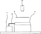
图1是本发明的实施方式的缺陷检查装置的主视图。FIG. 1 is a front view of a defect inspection device according to an embodiment of the present invention.
图2是缺陷检查装置的俯视图。Fig. 2 is a plan view of the defect inspection device.
图3是缺陷检查装置的侧视图。Fig. 3 is a side view of the defect inspection device.
图4是晶圆载置台的剖视图。FIG. 4 is a cross-sectional view of the wafer mounting table.
图5A、5B是用于说明各拍摄部的拍摄区域的图。5A and 5B are diagrams for explaining the imaging area of each imaging unit.
图6是用于说明电阻率测量部的结构的图。FIG. 6 is a diagram for explaining the configuration of a resistivity measurement unit.
图7是用于说明透射光量测量部的结构的图。FIG. 7 is a diagram for explaining the configuration of a transmitted light amount measuring unit.
图8是表示电阻率与图像亮度的关系的图表。FIG. 8 is a graph showing the relationship between resistivity and image brightness.
具体实施方式 Detailed ways
下面,参照附图详细说明本发明的实施方式、本发明的优点。Hereinafter, embodiments of the present invention and advantages of the present invention will be described in detail with reference to the drawings.
根据附图详细说明本发明的实施方式。另外,本发明的技术范围并不限定于实施方式的具体构造。Embodiments of the present invention will be described in detail with reference to the drawings. In addition, the technical scope of the present invention is not limited to the specific configurations of the embodiments.
图1~图3是本发明的实施方式的缺陷检查装置1的主视图、俯视图及侧视图。缺陷检查装置1包括拍摄部2、用于照射带状红外光的线型光导出射口(对应“红外光照明部件”,以下称作“照明部件”)3、晶圆载置台4及图像处理部12。如图4所示,晶圆9被水平地保持于晶圆载置台4上。1 to 3 are a front view, a plan view, and a side view of a
拍摄部2作为拍摄元件而包括线传感器阵列。如图1所示,拍摄部2配置在被载置于晶圆载置台4上的晶圆9的上方。本实施方式中使用的线传感器阵列采用具有较高的析像度的元件,即使是微细的伤痕、缺陷也能够检测。The
线传感器阵列以直线状排列像素,具有扫描功能。为了利用线传感器阵列获得二维的图像,需要使检查对象物沿与线传感器阵列的扫描方向(排列像素的方向)正交的方向移动。在图1中,由于搭载于拍摄部2上的线传感器阵列的扫描方向是与纸面平行的方向,因此,只要利用直线运动载物台5使作为检查对象物的晶圆9沿与纸面垂直的方向(图2中的箭头A方向)移动,就能够利用线传感器阵列获得二维图像。The line sensor array has pixels arranged in a straight line and has a scanning function. In order to obtain a two-dimensional image using the line sensor array, it is necessary to move the inspection object in a direction perpendicular to the scanning direction (the direction in which pixels are arranged) of the line sensor array. In FIG. 1, since the scanning direction of the line sensor array mounted on the
由于能够利用线传感器阵列拍摄的范围受到限制,因此,为了拍摄超出该范围的范围的图像,将拍摄区域分割为多个区域。而且,配置用于拍摄各个区域的拍摄部2,利用各个拍摄部2所具有的线传感器阵列拍摄各个区域。在本实施方式中,如图5A、5B所示地将拍摄区域分为两个区域(右区域和左区域),在各个拍摄区域中分别配置拍摄部2,从而能获取晶圆9的整个面的拍摄图像。Since the range that can be captured by the line sensor array is limited, the imaging area is divided into a plurality of areas in order to capture an image beyond the range. Furthermore, the
作为拍摄部2的光学系统,可以采用远心光学系统。在采用远心光学系统时,即使拍摄对象与光学系统之间的距离改变,所拍摄的图像的尺寸也不会变,因此,能够正确地掌握缺陷的位置和尺寸。As the optical system of the
由于可见光不能透射晶圆9,因此,采用可见光的通常的照明无法进行透射观察,但只要是大于1100nm的波长(红外光),就能够透射晶圆9而进行透射观察。因此,作为光源7,采用主要发出大于1100nm的波长的红外光光源。Since visible light cannot pass through the
照明部件3以带状照明作为检查对象的晶圆9的拍摄范围。从光源7发出的波长大于1127nm的红外光经由光纤8而从照明部件3照射到晶圆9上。本实施方式所使用的照明部件3具有足够照明拍摄部2的拍摄区域的长度和宽度,并且使用透镜进行聚光,从而能够获得拍摄所需的足够强度的照明光。The
图8是相对于晶圆9的电阻率的值表示拍摄透射过晶圆9后的红外光时的亮度(以下称作“图像亮度”),表示在改变了从照明部件3照射出的照明光量(以下称作“光量”)时的晶圆9的图像亮度。在图8中,在晶圆9的图像亮度的值为90~130时,能够适当地拍摄晶圆9的内部,因此,调节照明部件3的光量,以使晶圆9的图像亮度为该范围。FIG. 8 shows the brightness (hereinafter referred to as "image brightness") when photographing the infrared light transmitted through the
本实施方式的照明部件3能够相对于晶圆9的电阻率自动地设定光量,使得晶圆9为最适合拍摄的图像亮度,根据晶圆9的电阻率将照明部件3设定为适当的光量。The
如图1~图3所示,晶圆载置台4形成为能够利用直线运动载物台5及导轨6沿箭头A方向移动。直线运动载物台5被精密加工过的轨道和与该轨道组合的直线导轨轴承引导,并且具有能够精密地定位的驱动部,使晶圆载置台4以恒定速度移动。导轨6由滑动轴套61和滑动轴62构成。导轨6支承晶圆载置台4的负载,并且使晶圆载置台4顺畅的移动。即,本实施方式的晶圆9的移动机构由晶圆载置台4、直线运动载物台5和导轨6构成。As shown in FIGS. 1 to 3 ,
本实施方式是使晶圆9相对于拍摄部2和照明部件3移动的构造,但并不限定于该构造,例如也可以将拍摄部2和照明部件3构成为能够相对于晶圆9移动,通过做成照明部件被载置于固定了的晶圆载置台4上的晶圆9并拍摄晶圆9的机构,来扫描整个晶圆9。This embodiment is a structure in which the
图6表示在调节照明部件3的光量时使用的、用于测量晶圆9的电阻率的电阻率测量部10的构造。利用测量探头10a在晶圆9的表面测量晶圆9的电阻率。通过根据该测量值调节光源7的强度来调节照明部件3的光量,从而使透射晶圆9的光量成为最适合拍摄晶圆9的缺陷的光量。FIG. 6 shows the configuration of a resistivity measurement section 10 for measuring the resistivity of the
在本实施方式中,拍摄部2的灵敏度能够根据晶圆9的电阻率的值来调节。例如,在仅调节照明部件3而不能获得足够适当地拍摄图像所需的透射光量的情况下,通过调整拍摄部2的灵敏度来实现适当地拍摄图像。即,使用由电阻率测量部10测量的电阻率的值同时调节照明部件3的光量和拍摄部2的灵敏度,从而能够获得晶圆9的适合拍摄缺陷的图像亮度。In this embodiment, the sensitivity of the
接着,说明本实施方式的缺陷检查装置1的功能和进行检查的工序。Next, the function of the
利用未图示的输送装置输送晶圆9,将晶圆9转移到晶圆载置台4上。本实施方式的晶圆保持构造不是利用把持装置等抓住晶圆9的构造,而是利用设置于晶圆9的边缘的锥形部或者不会影响缺陷检查的范围的缘部支承晶圆9的构造。The
照明部件3根据晶圆9的电阻率的值来调节光量。通过根据由电阻率测量部10测量的电阻率的值来改变光源7的输出,将照明部件3的光量调节为能获得最适合拍摄的透射光量。The
利用图6所示的电阻率测量部10来测量晶圆9的电阻率的值。可以在将晶圆9载置于晶圆载置台4上的状态下,使电阻率测量部10靠近晶圆9来进行测量,也可以在将晶圆9载置于晶圆载置台4上之前将晶圆9载置于具有电阻率测量部10的另外的载置台上,测量晶圆9的电阻率。The value of the resistivity of the
根据由电阻率测量部10测量的晶圆9的电阻率的值来改变光源7的强度从而调节照明部件3的光量。调节照明部件3的照明光,使得透射晶圆9的透射光量为足够拍摄部2进行拍摄的量。The intensity of the light source 7 is changed in accordance with the value of the resistivity of the
利用直线运动载物台5使晶圆9沿恒定方向、以恒定速度移动,利用两个拍摄部2拍摄由晶圆9的透射光产生的影像。由于搭载于拍摄部2上的拍摄元件是以线状排列像素的线传感器阵列,因此,一边在沿各拍摄元件所排列的主扫描方向进行扫描的同时使晶圆9沿副扫描方向(图2中的箭头A方向)移动,一边进行反复扫描,从而获得二维的图像。The
拍摄部2的线传感器阵列能够拍摄的范围存在限制。因此,例如对于直径为300mm的晶圆来说,如图5A、5B所示地分割为两个拍摄范围,利用各自对应的拍摄部2进行拍摄。The imaging range of the line sensor array of the
从被调节为最适合拍摄的光量的照明部件3发出的照明光透射晶圆9,到达设置于拍摄部2上的线传感器阵列。只要在晶圆9的表面或者内部存在裂纹或者气泡,透射光就会在该位置折射而在线传感器阵列的拍摄图像中产生浓淡差。在晶圆9的表面或者内部存在裂纹的情况下能获得线状的图像,在晶圆9的表面或者内部存在气泡的情况下能获得圆状或圆环状的图像。图像处理部12根据它们的形状及浓度的信息来辨别缺陷。Illumination light emitted from the
调节照明部件3的光量的方法并不限定于根据由上述电阻率测量部10测量的电阻率的值来进行调整的方法。在前工序中测量电阻率的情况下,也可以针对每个晶圆将该值数据化而存储,根据该值调节照明部件3的光量。例如将被输送到缺陷检查装置1的晶圆9的电阻率的值预先存储于未图示的存储装置中,在晶圆9被转移到缺陷检查装置1之后从存储装置中取出该晶圆9的值,根据该值调节光源7的输出,将照明部件3的光量调节为透射晶圆9的、最适合拍摄晶圆9的缺陷的光量。The method of adjusting the light intensity of the
在该方法中,不必在缺陷检查装置1内设置电阻率测量部10。还具有这样的优点:在转移晶圆9时,能够早已预先将照明部件3的光量设定为最适合拍摄的光量,从而能够缩短检查所需的时间。In this method, it is not necessary to provide the resistivity measurement unit 10 in the
另外,能够根据晶圆9的电阻率的值来调节拍摄部2的灵敏度,通过使用预先测量的电阻率的值同时调节照明部件3的光量和拍摄部2的灵敏度,能够获得更加适合拍摄缺陷的晶圆9的图像亮度。In addition, the sensitivity of the
并且,图7表示设有透射光量测量部11的例子,该透射光量测量部11用于测量由照明部件3等红外光照明部照明时透射晶圆9的透射光的量。由透射光量测量部11测量的透射光量与晶圆9的图像亮度存在密切的关系,透射光量越大,晶圆9的图像亮度越高,透射光量较越小,晶圆9的图像亮度越低。由此,也可以使用透射晶圆9的光量的值来调节照明部件3的光量。作为此时使用的红外光照明部件,可以采用照明部件3,但并不限定于该构造,也可以设置用于测量透射光量的专用的照明部件。7 shows an example in which a transmitted light
另外,能够根据晶圆9的电阻率的值来调节拍摄部2的灵敏度,通过使用晶圆9的透射光量的值同时调节照明部件3的光量和拍摄部2的灵敏度,能够获得晶圆9的更加适合拍摄缺陷的图像亮度。In addition, the sensitivity of the
另外,作为调节照明部件3的光量的方法,对利用专门设置的电阻率测量部10的测量值的方法、使用预先测量的电阻率的值的方法、利用红外光的透射量的方法进行了说明,但并不限定于此。In addition, as the method of adjusting the light quantity of the illuminating
在本实施方式中,由两个拍摄部2覆盖晶圆9的整个面,但拍摄部2的数量并不限定于此。将许多个拍摄部2配置为一列而提高分辨率,能够获得更加精细的检查图像。In this embodiment, the entire surface of
像以上说明的那样,本发明的实施方式的缺陷检查装置1通过将对红外光具有灵敏度的线传感器阵列用作拍摄元件,能够在相同的检查条件下检查整个晶圆9,并且也能够应对检查工序的高速化。另外,通过获取晶圆9的电阻率的值,将照明部件3的光量设定为与获取的电阻率的值相对应的值,能够获得最适合拍摄缺陷的照明。结果,能够对以往透射检查存在困难的大直径的低电阻晶圆,在其整个面均匀且高速地检查缺陷。As described above, the
本申请基于2008年6月27日向日本国特许厅提交的日本特愿2008-192829主张优先权,通过参照将日本特愿2008-192829的全部内容编入本说明书中。This application claims priority based on Japanese Patent Application No. 2008-192829 filed with Japan Patent Office on June 27, 2008, and the entire contents of Japanese Patent Application No. 2008-192829 are incorporated into this specification by reference.
Claims (6)
Applications Claiming Priority (3)
| Application Number | Priority Date | Filing Date | Title |
|---|---|---|---|
| JP2008192829A JP4358889B1 (en) | 2008-06-27 | 2008-06-27 | Wafer defect inspection equipment |
| JP2008-192829 | 2008-06-27 | ||
| PCT/JP2008/072725 WO2009157105A1 (en) | 2008-06-27 | 2008-12-09 | Apparatus for inspecting silicon wafer defect and method for inspecting silicon wafer defect |
Publications (2)
| Publication Number | Publication Date |
|---|---|
| CN101933130A CN101933130A (en) | 2010-12-29 |
| CN101933130B true CN101933130B (en) | 2013-07-24 |
Family
ID=41393491
Family Applications (1)
| Application Number | Title | Priority Date | Filing Date |
|---|---|---|---|
| CN2008801007852A Expired - Fee Related CN101933130B (en) | 2008-06-27 | 2008-12-09 | Silicon wafer defect inspection device and defect inspection method |
Country Status (5)
| Country | Link |
|---|---|
| US (1) | US8654191B2 (en) |
| JP (1) | JP4358889B1 (en) |
| KR (1) | KR101296015B1 (en) |
| CN (1) | CN101933130B (en) |
| WO (1) | WO2009157105A1 (en) |
Families Citing this family (31)
| Publication number | Priority date | Publication date | Assignee | Title |
|---|---|---|---|---|
| CN102378909B (en) * | 2009-04-30 | 2014-07-02 | 威尔科克斯联营公司 | An inspection method and an inspection apparatus |
| KR101214806B1 (en) | 2010-05-11 | 2012-12-24 | 가부시키가이샤 사무코 | Apparatus and method for defect inspection of wafer |
| JP5556346B2 (en) * | 2010-05-11 | 2014-07-23 | 株式会社Sumco | Wafer defect inspection apparatus and wafer defect inspection method |
| US10460998B2 (en) * | 2010-11-09 | 2019-10-29 | Nikon Corporation | Method for inspecting substrate, substrate inspection apparatus, exposure system, and method for producing semiconductor device |
| JP6004517B2 (en) * | 2011-04-19 | 2016-10-12 | 芝浦メカトロニクス株式会社 | Substrate inspection apparatus, substrate inspection method, and adjustment method of the substrate inspection apparatus |
| EP2600323A3 (en) * | 2011-11-30 | 2013-12-25 | AIT Austrian Institute of Technology GmbH | Method and a device for recording a digital image with accurate colours |
| CN102569119A (en) * | 2011-12-19 | 2012-07-11 | 立晔科技股份有限公司 | Chip or wafer inspection device |
| CN102788802A (en) * | 2012-08-29 | 2012-11-21 | 苏州天准精密技术有限公司 | A multi-camera workpiece quality detection method |
| DE102012111835A1 (en) | 2012-12-05 | 2014-06-05 | Hseb Dresden Gmbh | inspection device |
| JP6059000B2 (en) * | 2012-12-12 | 2017-01-11 | 株式会社安永 | Wafer defect inspection system |
| CN103630545A (en) * | 2013-11-20 | 2014-03-12 | 江苏大学 | Injection-molded blade on-line monitoring device and method based on near-infrared optical wave array |
| JP6036670B2 (en) * | 2013-12-10 | 2016-11-30 | 信越半導体株式会社 | Defect concentration evaluation method for silicon single crystal substrate |
| CN106290390B (en) * | 2015-05-24 | 2019-11-26 | 上海微电子装备(集团)股份有限公司 | Defect detecting device and method |
| JP6402703B2 (en) * | 2015-11-17 | 2018-10-10 | 信越半導体株式会社 | Defect area determination method |
| US10692204B2 (en) * | 2016-08-01 | 2020-06-23 | The Boeing Company | System and method for high speed surface and subsurface FOD and defect detection |
| JP2018121031A (en) * | 2017-01-27 | 2018-08-02 | 株式会社ディスコ | Laser processing equipment |
| JP6975551B2 (en) * | 2017-05-18 | 2021-12-01 | ファスフォードテクノロジ株式会社 | Semiconductor manufacturing equipment and methods for manufacturing semiconductor equipment |
| US11060980B2 (en) * | 2017-11-29 | 2021-07-13 | Taiwan Semiconductor Manufacturing Co., Ltd. | Broadband wafer defect detection |
| CN108831844B (en) * | 2018-06-26 | 2019-12-06 | 长江存储科技有限责任公司 | Method and system for detecting wafer defects |
| TWI705244B (en) * | 2018-07-31 | 2020-09-21 | 由田新技股份有限公司 | Semiconductor defects inspection apparatus |
| EP3640630B1 (en) * | 2018-10-18 | 2026-03-11 | Infineon Technologies AG | Embedded wafer inspection |
| CN109712912B (en) * | 2018-12-06 | 2023-07-18 | 通富微电子股份有限公司 | Chip flip-chip equipment and method |
| CN110487814A (en) * | 2019-08-13 | 2019-11-22 | 东莞市创明电池技术有限公司 | Defect detection device for battery aluminum sheets |
| JP7382762B2 (en) * | 2019-08-27 | 2023-11-17 | 株式会社ディスコ | How to judge the quality of processing results of laser processing equipment |
| CN110645904B (en) * | 2019-10-17 | 2025-07-04 | 武汉大学 | A three-dimensional online monitoring method and device for packaging module warping deformation and defects |
| KR102453258B1 (en) | 2020-01-15 | 2022-10-11 | 주식회사 커미조아 | Apparatus and Method for Detecting of Awafer Edge |
| CN111307819B (en) * | 2020-03-16 | 2024-03-08 | 上海华力微电子有限公司 | Wafer edge defect detection system and method |
| CN111554601B (en) * | 2020-04-27 | 2021-12-28 | 上海果纳半导体技术有限公司 | Wafer front end transfer system |
| CN112730252A (en) * | 2020-12-30 | 2021-04-30 | 湖南三安半导体有限责任公司 | Wafer detection device |
| CN115931908B (en) * | 2022-12-28 | 2024-05-07 | 杭州中为光电技术有限公司 | Automatic detection system and detection method for silicon rod defects |
| CN119643585B (en) * | 2025-02-19 | 2025-06-06 | 华芯半导体科技有限公司 | Chip defect detection system and method based on visual recognition |
Family Cites Families (19)
| Publication number | Priority date | Publication date | Assignee | Title |
|---|---|---|---|---|
| JPS627200A (en) * | 1985-07-03 | 1987-01-14 | 株式会社日立製作所 | Bonding state detection device |
| US5196375A (en) * | 1987-07-24 | 1993-03-23 | Kabushiki Kaisha Toshiba | Method for manufacturing bonded semiconductor body |
| JPH03265152A (en) * | 1990-03-15 | 1991-11-26 | Fujitsu Ltd | Measuring method for temperature of wafer |
| JPH06102197A (en) * | 1992-09-21 | 1994-04-15 | Kawasaki Steel Corp | Surface defect detection method |
| JP3338118B2 (en) | 1993-05-10 | 2002-10-28 | 株式会社日立製作所 | Method for manufacturing semiconductor device |
| JPH08220008A (en) * | 1995-02-15 | 1996-08-30 | Mitsubishi Electric Corp | Infrared inspection equipment |
| JPH09311108A (en) | 1996-05-24 | 1997-12-02 | Nikon Corp | Defect inspection device and defect inspection method |
| JPH10253546A (en) * | 1997-03-12 | 1998-09-25 | Toshiba Corp | Method and apparatus for evaluating semiconductor substrate |
| JPH10325805A (en) * | 1997-05-23 | 1998-12-08 | Nikon Corp | Automatic inspection equipment for semiconductor wafers |
| JP3874562B2 (en) * | 1998-02-19 | 2007-01-31 | 日本コントロールシステム株式会社 | Glass plate crushing test method, apparatus and glass test imaging method |
| US6597444B1 (en) * | 2000-06-28 | 2003-07-22 | Advanced Micro Devices, Inc. | Determination of flux coverage |
| JP2002340794A (en) * | 2001-05-15 | 2002-11-27 | Sumitomo Mitsubishi Silicon Corp | Method for measuring infrared absorption of semiconductor wafer |
| JP4596968B2 (en) * | 2005-05-11 | 2010-12-15 | 株式会社リコー | Silicon substrate processing method and defective portion identification method for observing defective portion of semiconductor device |
| JP4693642B2 (en) * | 2006-01-30 | 2011-06-01 | 株式会社東芝 | Semiconductor device manufacturing method and cleaning apparatus |
| JP4864504B2 (en) * | 2006-03-24 | 2012-02-01 | Sumco Techxiv株式会社 | Crystal wafer inspection method and apparatus for silicon wafer |
| SG138524A1 (en) * | 2006-06-22 | 2008-01-28 | Siltronic Ag | Method and apparatus for detection of mechanical defects in an ingot piece composed of semiconductor material |
| JP2008008636A (en) * | 2006-06-27 | 2008-01-17 | Reitetsukusu:Kk | Calibration method for edge inspection equipment |
| JP2008198966A (en) * | 2007-02-08 | 2008-08-28 | Nippon Electro Sensari Device Kk | Wafer defect inspection device |
| JP2011033449A (en) * | 2009-07-31 | 2011-02-17 | Sumco Corp | Method and apparatus for defect inspection of wafer |
-
2008
- 2008-06-27 JP JP2008192829A patent/JP4358889B1/en active Active
- 2008-12-09 CN CN2008801007852A patent/CN101933130B/en not_active Expired - Fee Related
- 2008-12-09 US US12/451,703 patent/US8654191B2/en active Active
- 2008-12-09 KR KR1020097025835A patent/KR101296015B1/en active Active
- 2008-12-09 WO PCT/JP2008/072725 patent/WO2009157105A1/en not_active Ceased
Also Published As
| Publication number | Publication date |
|---|---|
| JP4358889B1 (en) | 2009-11-04 |
| US8654191B2 (en) | 2014-02-18 |
| KR20100023861A (en) | 2010-03-04 |
| JP2010008392A (en) | 2010-01-14 |
| CN101933130A (en) | 2010-12-29 |
| KR101296015B1 (en) | 2013-08-12 |
| US20100165095A1 (en) | 2010-07-01 |
| WO2009157105A1 (en) | 2009-12-30 |
Similar Documents
| Publication | Publication Date | Title |
|---|---|---|
| CN101933130B (en) | Silicon wafer defect inspection device and defect inspection method | |
| US11892414B2 (en) | Device and method for checking for surface defect, using image sensor | |
| US9140545B2 (en) | Object inspection system | |
| KR101547649B1 (en) | Inspection apparatus | |
| WO2008110061A1 (en) | Plane substrate auto-test system and the method thereof | |
| JP2007278928A (en) | Defect inspection device | |
| TW200839227A (en) | Automatic inspection system for flat panel substrate | |
| TWI333544B (en) | Substrate inspection apparatus | |
| CN110402386A (en) | Cylinder surface examining device and cylinder surface inspecting method | |
| CN100520380C (en) | Inspecting apparatus, image pickup apparatus, and inspecting method | |
| EP3594665A1 (en) | Optical inspection device and method | |
| JP2008198966A (en) | Wafer defect inspection device | |
| JP5393973B2 (en) | Rod lens array inspection apparatus and method | |
| JP2009236760A (en) | Image detection device and inspection apparatus | |
| JPH11248643A (en) | Foreign film inspection device for transparent film | |
| JP2005274156A (en) | Flaw inspection device | |
| JP2004212353A (en) | Optical inspection apparatus | |
| CN118425154A (en) | Device for detecting surface defects in objects | |
| JP2006292412A (en) | Surface inspection system, surface inspection method and substrate manufacturing method | |
| KR102528464B1 (en) | Vision Inspecting Apparatus | |
| JP2002131240A (en) | Management method of foreign substance inspection in through hole | |
| JP2007285869A (en) | Surface inspection apparatus and surface inspection method | |
| JP2007147441A (en) | Inspection device | |
| JP2006003168A (en) | Method and apparatus for measuring surface shape | |
| JPH09297107A (en) | Defect inspection apparatus and adjustment method thereof |
Legal Events
| Date | Code | Title | Description |
|---|---|---|---|
| C06 | Publication | ||
| PB01 | Publication | ||
| C10 | Entry into substantive examination | ||
| SE01 | Entry into force of request for substantive examination | ||
| C14 | Grant of patent or utility model | ||
| GR01 | Patent grant | ||
| CF01 | Termination of patent right due to non-payment of annual fee | ||
| CF01 | Termination of patent right due to non-payment of annual fee |
Granted publication date: 20130724 Termination date: 20211209 |