CN101903128A - Chamfering processing method and chamfering processing device for brittle material substrate - Google Patents
Chamfering processing method and chamfering processing device for brittle material substrate Download PDFInfo
- Publication number
- CN101903128A CN101903128A CN2008801215041A CN200880121504A CN101903128A CN 101903128 A CN101903128 A CN 101903128A CN 2008801215041 A CN2008801215041 A CN 2008801215041A CN 200880121504 A CN200880121504 A CN 200880121504A CN 101903128 A CN101903128 A CN 101903128A
- Authority
- CN
- China
- Prior art keywords
- chamfering
- substrate
- edge line
- laser beam
- laser
- Prior art date
- Legal status (The legal status is an assumption and is not a legal conclusion. Google has not performed a legal analysis and makes no representation as to the accuracy of the status listed.)
- Granted
Links
Images




Classifications
-
- B—PERFORMING OPERATIONS; TRANSPORTING
- B28—WORKING CEMENT, CLAY, OR STONE
- B28D—WORKING STONE OR STONE-LIKE MATERIALS
- B28D5/00—Fine working of gems, jewels, crystals, e.g. of semiconductor material; apparatus or devices therefor
-
- B—PERFORMING OPERATIONS; TRANSPORTING
- B23—MACHINE TOOLS; METAL-WORKING NOT OTHERWISE PROVIDED FOR
- B23K—SOLDERING OR UNSOLDERING; WELDING; CLADDING OR PLATING BY SOLDERING OR WELDING; CUTTING BY APPLYING HEAT LOCALLY, e.g. FLAME CUTTING; WORKING BY LASER BEAM
- B23K26/00—Working by laser beam, e.g. welding, cutting or boring
- B23K26/08—Devices involving relative movement between laser beam and workpiece
- B23K26/082—Scanning systems, i.e. devices involving movement of the laser beam relative to the laser head
-
- B—PERFORMING OPERATIONS; TRANSPORTING
- B23—MACHINE TOOLS; METAL-WORKING NOT OTHERWISE PROVIDED FOR
- B23K—SOLDERING OR UNSOLDERING; WELDING; CLADDING OR PLATING BY SOLDERING OR WELDING; CUTTING BY APPLYING HEAT LOCALLY, e.g. FLAME CUTTING; WORKING BY LASER BEAM
- B23K26/00—Working by laser beam, e.g. welding, cutting or boring
- B23K26/08—Devices involving relative movement between laser beam and workpiece
- B23K26/082—Scanning systems, i.e. devices involving movement of the laser beam relative to the laser head
- B23K26/0821—Scanning systems, i.e. devices involving movement of the laser beam relative to the laser head using multifaceted mirrors, e.g. polygonal mirror
-
- B—PERFORMING OPERATIONS; TRANSPORTING
- B23—MACHINE TOOLS; METAL-WORKING NOT OTHERWISE PROVIDED FOR
- B23K—SOLDERING OR UNSOLDERING; WELDING; CLADDING OR PLATING BY SOLDERING OR WELDING; CUTTING BY APPLYING HEAT LOCALLY, e.g. FLAME CUTTING; WORKING BY LASER BEAM
- B23K26/00—Working by laser beam, e.g. welding, cutting or boring
- B23K26/36—Removing material
- B23K26/40—Removing material taking account of the properties of the material involved
-
- B—PERFORMING OPERATIONS; TRANSPORTING
- B23—MACHINE TOOLS; METAL-WORKING NOT OTHERWISE PROVIDED FOR
- B23K—SOLDERING OR UNSOLDERING; WELDING; CLADDING OR PLATING BY SOLDERING OR WELDING; CUTTING BY APPLYING HEAT LOCALLY, e.g. FLAME CUTTING; WORKING BY LASER BEAM
- B23K2101/00—Articles made by soldering, welding or cutting
- B23K2101/36—Electric or electronic devices
- B23K2101/40—Semiconductor devices
-
- B—PERFORMING OPERATIONS; TRANSPORTING
- B23—MACHINE TOOLS; METAL-WORKING NOT OTHERWISE PROVIDED FOR
- B23K—SOLDERING OR UNSOLDERING; WELDING; CLADDING OR PLATING BY SOLDERING OR WELDING; CUTTING BY APPLYING HEAT LOCALLY, e.g. FLAME CUTTING; WORKING BY LASER BEAM
- B23K2103/00—Materials to be soldered, welded or cut
- B23K2103/50—Inorganic materials other than metals or composite materials
Landscapes
- Physics & Mathematics (AREA)
- Optics & Photonics (AREA)
- Engineering & Computer Science (AREA)
- Mechanical Engineering (AREA)
- Plasma & Fusion (AREA)
- Laser Beam Processing (AREA)
- Re-Forming, After-Treatment, Cutting And Transporting Of Glass Products (AREA)
- Processing Of Stones Or Stones Resemblance Materials (AREA)
Abstract
Description
技术领域technical field
本发明涉及在脆性材料基板端面形成的边缘线(棱线)的倒角加工方法,进一步详细而言,涉及通过照射激光束进行边缘线的圆弧倒角或斜面倒角的倒角加工方法和倒角加工装置。The present invention relates to a chamfering method of an edge line (ridge line) formed on an end surface of a brittle material substrate. Chamfering processing device.
在此,作为加工对象的脆性材料基板除了玻璃基板以外,还包括石英、单结晶硅、蓝宝石、半导体晶片、陶瓷等基板。Here, the brittle material substrates to be processed include substrates such as quartz, single crystal silicon, sapphire, semiconductor wafers, and ceramics, in addition to glass substrates.
背景技术Background technique
玻璃基板等脆性材料基板通过加工成预期的尺寸、形状而被用于各种产品。一般而言,脆性材料基板的加工利用切割(dicing)、砂轮划线(wheel scribe)、激光划线(laser scribe)等现有的加工技术进行,然而利用这些加工技术分割的基板端面的边缘线非常锋利,存在仅施加微小的冲击都会产生碎屑(chipping)、微裂纹(microcrack)等不良情况。例如,在平板显示器(FPD)用玻璃基板中,因边缘缺损而产生的碎片会导致在FPD用基板的表面产生损伤,对产品的成品合格率造成影响。Brittle material substrates such as glass substrates are processed into desired sizes and shapes and used in various products. Generally speaking, the processing of brittle material substrates is carried out using existing processing technologies such as dicing, wheel scribe, and laser scribe. It is very sharp, and there are disadvantages such as chipping and microcracks even when a slight impact is applied. For example, in glass substrates for flat panel displays (FPDs), fragments generated due to edge defects cause damage to the surface of the substrates for FPDs, affecting the yield of products.
因此,为了防止在将基板分割后产生的基板的边缘部分的缺损等,沿边缘线进行倒角加工。Therefore, chamfering is performed along the edge line in order to prevent chipping or the like of the edge portion of the substrate that occurs after the substrate is divided.
现有的倒角加工中的一种为湿式研磨法:一边供应大量的水一边利用金刚石磨石进行研磨。然而,在利用湿式研磨法形成的倒角加工面上,连续残存有微小的裂纹,使倒角加工面的强度比周围显著降低。One of the conventional chamfering processes is a wet grinding method in which grinding is performed with a diamond grindstone while supplying a large amount of water. However, micro cracks continue to remain on the chamfered surface formed by the wet grinding method, so that the strength of the chamfered surface is significantly lower than that of the surrounding area.
相对于此,提出有加热熔融法:沿着要进行倒角加工的边缘线扫描激光束,并沿边缘线移动激光束的焦点而将边缘上加热熔融,由此进行倒角。例如公开有如下方法:在将玻璃部件整体保持比常温高的温度(余热)的状态下,对棱线部附近进行激光加热,使棱线部软化而变圆,由此进行倒角(参考专利文献1)。On the other hand, there has been proposed a heating and melting method in which a laser beam is scanned along an edge line to be chamfered, and the focus of the laser beam is moved along the edge line to heat and melt the edge, thereby performing chamfering. For example, there is disclosed a method of chamfering the edges by heating the vicinity of the ridges with a laser while keeping the entire glass member at a temperature higher than normal temperature (excess heat) to soften and round the ridges (refer to Patent No. Literature 1).
图8是表示使用CO2激光光源通过加热熔融法进行倒角加工时的激光照射状态的剖视图。预先使用未图示的加热器将玻璃基板10整体逐渐加热至比软化温度低的预定温度,接着沿被保持于预定温度的玻璃基板10的要进行倒角加工的边缘线51,利用聚光透镜53将来自CO2激光光源50的激光聚光,将焦点对准加工部分附近进行扫描。此时,通过调整激光输出、扫描速度,使被激光照射到的边缘部分升至高温并软化,由此加工成使激光照射后的边缘部分带有圆度。8 is a cross-sectional view showing a state of laser irradiation when chamfering is performed by a heating and melting method using a CO 2 laser light source. The
此时,预热和加工后的冷却耗费时间。此外,必须将基板整体预热,当在基板上已形成无法加热的器件、传感器等的功能膜的情况下,有时无法利用此方法实施倒角加工。此外,若余热不足则会因热应力产生裂缝(裂纹),无法进行良好的倒角加工。再有,在上述的加热熔融法的倒角加工中,有时熔融部分会变形导致其一部分(带有圆度的部分的局部)相对于周围膨胀,有损于基板端面的平面度。In this case, preheating and cooling after processing take time. In addition, the entire substrate must be preheated, and when functional films such as devices and sensors that cannot be heated are formed on the substrate, it may not be possible to perform chamfering by this method. In addition, if the residual heat is insufficient, cracks (cracks) will be generated due to thermal stress, and good chamfering cannot be performed. In addition, in the chamfering process of the above-mentioned heating and melting method, the melted portion may be deformed and a part thereof (part of the rounded portion) may expand relative to the surroundings, thereby impairing the flatness of the end surface of the substrate.
作为与加热熔融法不同的、无须预热的激光照射的倒角方法,已公开有如下的激光划线法:通过将激光照射至边缘附近进行加热,使玻璃基板10产生裂纹,并通过使激光相对地沿边缘线方向进行扫描,使裂纹沿边缘线成长,将边缘附近从玻璃基板分离,由此进行倒角(专利文献2)。As a chamfering method of laser irradiation that does not require preheating different from the heating and melting method, there is disclosed a laser scribing method in which cracks are generated in the
图9是表示使用CO2激光光源通过激光划线进行倒角加工时的激光照射状态的图。来自CO2激光光源50的激光通过聚光透镜53局部地照射于玻璃基板10的边缘线51附近,以比软化温度低的温度进行加热。此时,随着与局部热膨胀相伴的热应力产生裂纹52。进而,通过沿边缘线51扫描激光,依次产生的裂纹52沿边缘线51成长,包含边缘线51的边缘附近(角部分)被分离。Fig. 9 is a diagram showing a laser irradiation state when chamfering is performed by laser scribing using a CO2 laser light source. The laser light from the CO 2
根据专利文献2,通过进行激光划线的倒角加工,能够在不损及玻璃基板精度的情况下实施高生产性且无须清洗工序的倒角加工。According to Patent Document 2, by performing chamfering processing of laser scribing, it is possible to perform chamfering processing with high productivity and without a cleaning process without impairing the precision of the glass substrate.
专利文献1:日本特开平2-241684号公报Patent Document 1: Japanese Patent Application Laid-Open No. 2-241684
专利文献2:日本特开平9-225665号公报Patent Document 2: Japanese Patent Application Laid-Open No. 9-225665
此处,针对通过激光划线的倒角加工形成的加工面进行说明。图10是通过使用CO2激光的激光划线进行倒角加工时的加工剖面的放大图。Here, the processed surface formed by the chamfering process of laser scribing will be described. Fig. 10 is an enlarged view of a processed section when chamfering is performed by laser scribing using a CO2 laser.
通过倒角加工,玻璃基板10的角部分U被分离(剥离),玻璃基板10的边缘线53与角部分U一起消失,但重新形成有倒角加工面54。The corner portion U of the
观察该倒角加工面54的截面形状,具有向玻璃基板10侧凹陷的圆弧状的倒圆弧面。倒角加工面54凹陷的结果是,在与玻璃基板10的基板表面55、56交叉的部分形成两条边缘线57、58。与原来的边缘线53相比,这些边缘线57、58的边缘的锋利度有所改善,不过虽然如此,如果凹陷变大的话,还是会形成锋利的边缘。When the cross-sectional shape of the
特别是在平板显示器用(FPD用)玻璃基板中,有时会在边缘线57、58正上方实施TAB(Tape Automated Bonding:卷带自动结合)卷带的配线,在倒角加工之后,如果在该部分残留有锋利的边缘,则TAB卷带断线的可能性会变高。Especially in flat panel display (FPD) glass substrates, TAB (Tape Automated Bonding: Tape Automated Bonding) wiring is sometimes performed directly above the
因此,对于倒角加工面54,要求消除凹陷且将倒角部分形成为作为平面的斜面(C面)或朝向外侧呈凸状的圆弧面(R面)。Therefore, for the chamfered
然而,通过上述现有的使用CO2激光的激光划线法形成的倒角加工面54总是会在倒角加工面产生凹陷。即使改变向边缘线53照射的激光的照射方向,其结果还是大致相同,难以控制倒角加工面的形状。However, the chamfered
近年来,在平板显示器(FPD)用玻璃基板等中,采用了比以往更大型的玻璃基板,随着玻璃基板的大型化,对基板的加工质量也逐渐要求比目前更高的精度、可靠性。针对倒角加工面的形状,也要求比目前更高的精度和可靠性。In recent years, larger glass substrates have been used in glass substrates for flat panel displays (FPDs), etc. As the size of glass substrates has increased, higher precision and reliability have been required for the processing quality of substrates. . For the shape of the chamfered surface, higher precision and reliability than before are required.
发明内容Contents of the invention
因此,本发明的目的在于提供一种倒角加工方法及倒角加工装置,能够使通过激光照射形成的倒角加工面不是倒圆弧面,而形成为斜面、圆弧面、或朝向外侧呈凸状的曲面。Therefore, the object of the present invention is to provide a chamfering processing method and a chamfering processing device, which can make the chamfering processing surface formed by laser irradiation not a chamfering arc surface, but a slope, an arc surface, or a chamfering surface toward the outside. Convex surface.
为了解决上述课题而做出的本发明的倒角加工方法并非从要进行倒角加工的边缘线前方的空间照射激光束并加热该边缘线,而是使从基板背侧穿透基板内的激光束在边缘线附近聚光,并且在扫描与边缘线交叉的面内的同时进行加热,通过消融进行倒角加工。In order to solve the above-mentioned problems, the chamfering method of the present invention does not irradiate the laser beam from the space in front of the edge line to be chamfered to heat the edge line, but makes the laser beam penetrate the substrate from the backside of the substrate. The beam is focused near the edge line and heated while scanning the surface intersecting the edge line, and chamfering is performed by ablation.
即,对进行脆性材料基板的倒角加工的边缘线以穿透基板内的方式照射激光束,并且将聚光部件配置于激光束的光路上,在边缘线附近的基板表面或基板内部形成激光束的会聚点,在与边缘线交叉的面内对与倒角加工的加工预定宽度对应的范围扫描会聚点,通过会聚点附近的消融处理沿会聚点的扫描轨迹进行倒角加工。That is, a laser beam is irradiated on the edge line of the brittle material substrate to be chamfered so as to penetrate into the substrate, and a light-condensing member is arranged on the optical path of the laser beam to form a laser beam on the surface of the substrate near the edge line or inside the substrate. For the convergent point of the beam, the convergent point is scanned in a range corresponding to the expected width of chamfering in the plane intersecting the edge line, and the chamfering process is performed along the scanning trajectory of the convergent point by ablation processing near the convergent point.
此处,脆性材料基板包括玻璃基板、石英基板、硅基板、蓝宝石基板、硅及其他的半导体晶片、陶瓷基板。Here, the brittle material substrate includes glass substrates, quartz substrates, silicon substrates, sapphire substrates, silicon and other semiconductor wafers, and ceramic substrates.
照射至脆性材料基板的激光束根据进行倒角加工的基板材料来选择适当波长的激光。即,采用如下的波长光:在使激光束一边聚光一边向基板照射时,在会聚点附近产生由多光子吸收引起的消融现象,而在会聚点附近以外的激光束所通过的光路上几乎不被吸收。For the laser beam irradiated on the brittle material substrate, a laser beam with an appropriate wavelength is selected according to the substrate material to be chamfered. That is, the following wavelength light is used: when the laser beam is irradiated to the substrate while converging, the ablation phenomenon caused by multiphoton absorption occurs near the converging point, and the optical path passed by the laser beam other than the converging point is almost Not absorbed.
具体而言,例如对于玻璃基板,能够采用波长为193nm~1064nm的激光,作为激光光源能够采用Nd-YAG激光、ArF准分子激光、KrF准分子激光等。此外,例如对于硅基板,能够采用波长为1100nm以上的激光。Specifically, for example, for a glass substrate, laser light with a wavelength of 193 nm to 1064 nm can be used, and Nd-YAG laser, ArF excimer laser, KrF excimer laser, etc. can be used as a laser light source. In addition, for example, for a silicon substrate, laser light having a wavelength of 1100 nm or more can be used.
另一方面,对于加工对象物来说吸收率大而几乎无法穿透基板内的激光光源,无法用于本发明的倒角加工。例如对于玻璃基板来说,由于CO2激光、CO激光(波长为5.3μm)的吸收率大,因此几乎无法穿透玻璃基板内,因此在加工对象物为玻璃基板的情况下,将CO2激光、CO激光从本发明所使用的倒角加工用激光光源中排除。On the other hand, a laser light source that has a high absorption rate for the object to be processed and hardly penetrates into the substrate cannot be used for the chamfering process of the present invention. For example, for glass substrates, CO2 lasers and CO lasers (with a wavelength of 5.3 μm) have a large absorption rate, so they can hardly penetrate into the glass substrate. Therefore, when the object to be processed is a glass substrate, the CO2 laser , CO laser is excluded from the laser light source for chamfering used in the present invention.
配置于激光束的光路上的聚光部件只要是能发挥聚光功能的光学元件即可。具体而言,能够使用凸透镜(也包括多枚的组合凸透镜)或凹面镜。此外,在使倒角加工面形成预期的曲面(然而为了聚光而形成为凸状)的情况下,调整聚光部件的光学参数(折射率、曲率半径、曲面形状等),从而通过后述的射束偏转部沿该曲面形状扫描会聚点。The condensing member disposed on the optical path of the laser beam may be any optical element capable of performing a condensing function. Specifically, a convex lens (including a plurality of combined convex lenses) or a concave mirror can be used. In addition, when the chamfered surface is formed into a desired curved surface (however, it is formed into a convex shape for light collection), the optical parameters (refractive index, curvature radius, curved surface shape, etc.) The beam deflection section scans the converging point along the curved surface shape.
具体而言,会聚点的扫描轨迹除了球面(圆弧面)以外,例如形成为抛物面或椭圆面。此外,通过使聚光部件形成为所谓fθ透镜,也能够将倒角加工面形成为平面。Specifically, the scanning locus of the converging point is formed, for example, as a paraboloid or an ellipse other than a spherical surface (arc surface). In addition, by forming the light collecting member as a so-called fθ lens, the chamfered surface can also be formed as a flat surface.
根据本发明,相对于进行脆性材料基板的倒角加工的边缘线以穿透基板内的方式从背侧照射激光束。此时,将聚光部件配置于激光束的光路上,将激光束的会聚点形成于边缘线附近的基板表面或基板内部。进而,在与边缘线交叉的面内扫描会聚点。该扫描包含与倒角加工的加工预定宽度对应的范围。这样,通过聚光后的激光照射产生消融现象,使会聚点附近局部熔融并被除去。进而,通过在与边缘线交叉的面内扫描该会聚点,形成沿扫描轨迹的形状的倒角加工面。因此,利用聚光部件的光学参数来调整会聚点的扫描轨迹,以进行圆弧面、斜面的倒角加工。According to the present invention, the laser beam is irradiated from the back side so as to penetrate into the substrate with respect to the edge line to be chamfered on the brittle material substrate. In this case, the condensing member is arranged on the optical path of the laser beam, and the converging point of the laser beam is formed on the surface of the substrate near the edge line or inside the substrate. Furthermore, the converging point is scanned in the plane intersecting the edge line. This scan includes a range corresponding to the planned width of chamfering. In this way, the ablation phenomenon occurs by irradiation with laser light after focusing, and the vicinity of the point of convergence is locally melted and removed. Furthermore, by scanning this converging point in the plane intersecting the edge line, a chamfered surface having a shape along the scanning locus is formed. Therefore, the scanning trajectory of the converging point is adjusted by using the optical parameters of the converging part, so as to perform chamfering of arcuate surfaces and inclined surfaces.
根据本发明,能够将通过激光照射而形成的倒角加工面形成为斜面、圆弧面、或朝向外侧呈凸状的曲面。According to the present invention, the chamfered surface formed by laser irradiation can be formed as an inclined surface, an arc surface, or a curved surface convex toward the outside.
(其他的课题解决手段和效果)(Other problem solving methods and effects)
在上述发明中,也可以在使会聚点沿边缘线相对移动的同时重复在与边缘线交叉的面内的会聚点的扫描,从而沿边缘线进行倒角加工。In the above invention, chamfering may be performed along the edge line by repeating scanning of the point of convergence in a plane intersecting the edge line while relatively moving the point of convergence along the edge line.
由此,就边缘线而言,能够对整个边缘线进行倒角加工。在该情况下,可以从边缘线的起点至终点连续地相对移动,但是在进行较深的倒角加工的情况下,也可以视情况间歇地相对移动以赋予充分的能量,从而可靠地进行倒角加工。Thereby, as for the edge line, it is possible to chamfer the entire edge line. In this case, the relative movement can be performed continuously from the start point to the end point of the edge line, but in the case of deep chamfering, it is also possible to perform relative movement intermittently to give sufficient energy to reliably perform chamfering. Corner processing.
在上述发明中,也可以使会聚点在基板内的深度位置与倒角加工的加工预定深度对应地进行倒角加工。In the above invention, the chamfering may be performed so that the depth position of the converging point in the substrate corresponds to the planned depth of the chamfering.
由此,由于使会聚点在基板内的深度位置与倒角加工的加工预定深度对应,因此通过进行扫描能够一次便使倒角加工达到预定深度。Thus, since the depth position of the converging point in the substrate is made to correspond to the planned depth of chamfering, it is possible to chamfer to a predetermined depth by performing one scan.
在上述发明中,也可以重复多次所述会聚点向边缘线方向的相对移动,随着相对移动的移动次数增加,会聚点的深度位置就会向基板内部侧移位。In the above invention, the relative movement of the converging point toward the edge line may be repeated multiple times, and as the number of relative movements increases, the depth position of the converging point will shift toward the inner side of the substrate.
由此,在倒角加工的深度较深时,能够进行最初较浅并逐渐增加深度的倒角加工。Accordingly, when the depth of chamfering is deep, it is possible to perform chamfering that is initially shallow and gradually increases in depth.
此外,与上述发明相关并根据其他观点完成的本发明的倒角加工装置为对脆性材料基板进行倒角加工的倒角加工装置,该倒角加工装置具备:激光光源;聚光部件,所述聚光部件对从激光光源放射的激光束进行聚光;射束偏转部,所述射束偏转部设于激光光源和聚光部件之间的激光束的光路上,并以如下方式使激光束的行进方向偏转:扫描从激光光源放射的激光束向聚光部件照射的照射位置,并扫描从聚光部件射出的激光束所形成的会聚点;以及基板支撑部,所述基板支撑部构成为:在使所述激光束穿透基板内并进行倒角加工的边缘线附近的基板表面或基板内部使所述会聚点在与边缘线交叉的面内进行扫描,并且在边缘线露出于空间中的状态下支撑所述基板。In addition, the chamfering processing device of the present invention, which is related to the above invention and completed from other viewpoints, is a chamfering processing device for chamfering a brittle material substrate. The chamfering processing device includes: a laser light source; The condensing part condenses the laser beam radiated from the laser light source; the beam deflection part is arranged on the optical path of the laser beam between the laser light source and the condensing part, and makes the laser beam deflection in the direction of travel: scanning the irradiation position where the laser beam radiated from the laser light source is irradiated to the condensing member, and scanning the converging point formed by the laser beam emitted from the condensing member; and the substrate supporting part, the substrate supporting part is constituted as : The laser beam penetrates the substrate and performs chamfering on the substrate surface or inside the substrate near the edge line and scans the converging point in a plane intersecting the edge line, and exposes the edge line in space The substrate is supported in the state.
由此,在激光光源与聚光部件之间的激光束的光路上设置的射束偏转部扫描从激光光源放射的激光束向聚光部件照射的照射位置。聚光部件根据激光束的照射位置使激光束的射出方向偏转。其结果是,从聚光部件射出的激光束所形成的会聚点在边缘线附近且在与边缘线交叉的面内进行扫描,沿会聚点的扫描轨迹形成通过消融产生的倒角加工面。此时的会聚点的扫描轨迹由聚光部件的光学参数确定。一般而言,由于利用聚光部件形成的扫描轨迹朝向激光束的行进方向呈凸状(例如在聚光部件为凸透镜、凹面镜的情况下的扫描轨迹为呈凸状的弧),因此形成了与由聚光部件的光学参数所确定的凸状扫描轨迹对应的倒角加工面。Accordingly, the beam deflection unit provided on the optical path of the laser beam between the laser light source and the light-condensing member scans the irradiation position where the laser beam emitted from the laser light source is irradiated onto the light-condensing member. The condensing member deflects the emission direction of the laser beam according to the irradiation position of the laser beam. As a result, the converging point formed by the laser beam emitted from the condensing member is scanned near the edge line and in the plane intersecting the edge line, and a chamfered surface by ablation is formed along the scanning locus of the converging point. The scanning trajectory of the converging point at this time is determined by the optical parameters of the converging member. In general, since the scanning trajectory formed by the light-condensing member is convex toward the traveling direction of the laser beam (for example, the scanning trajectory is a convex arc when the light-condensing member is a convex lens or a concave mirror), a The chamfered processing surface corresponds to the convex scanning trajectory determined by the optical parameters of the light-collecting component.
在上述倒角加工装置中,也可以具备进给机构,所述进给机构使基板侧或激光束侧移动,以使会聚点沿边缘线相对移动。In the chamfering processing apparatus described above, a feed mechanism for moving the substrate side or the laser beam side so as to relatively move the converging point along the edge line may be provided.
由此,就边缘线而言,能够对整个边缘线进行倒角加工。Thereby, as for the edge line, it is possible to chamfer the entire edge line.
在上述倒角加工装置中,基板支撑部也可以由水平地载置基板的工作台构成,并且聚光部件和射束偏转部被配置成使激光束相对于基板倾斜入射。In the chamfering processing apparatus described above, the substrate supporting unit may be constituted by a table on which the substrate is placed horizontally, and the light condensing member and the beam deflecting unit may be arranged so that the laser beam is obliquely incident on the substrate.
由此,能够在将基板稳定地载置于水平的工作台上的状态下进行倒角加工。Thereby, chamfering processing can be performed in the state which mounted the board|substrate stably on the horizontal table.
在该情况下,也可以构成为,聚光部件和射束偏转部被配置成使激光束相对于基板从上方倾斜入射,在进行倒角加工的边缘线在从工作台面的外侧离开的位置朝向下方露出的状态下被支撑。In this case, the converging member and the beam deflecting unit may be arranged so that the laser beam is obliquely incident on the substrate from above, and the edge line to be chamfered faces away from the outside of the table surface. It is supported while the bottom is exposed.
由此,由于进行倒角加工的边缘线朝向下方,因此利用消融除去的基板材料的残渣向下方扩散,由此可减少附着在基板上的附着量。As a result, since the edge line to be chamfered faces downward, the residue of the substrate material removed by ablation diffuses downward, thereby reducing the amount of adhesion to the substrate.
在上述倒角加工装置中,射束偏转部也可以由电流镜(Galvanomirror)或多面镜(polygon mirror)构成。In the chamfering device described above, the beam deflection unit may be constituted by a galvano mirror or a polygon mirror.
在电流镜的情况下通过反射镜的摆动运动,而在多面镜的情况下则通过反射镜的旋转运动,都能够使朝向聚光部件的激光束偏转。Both in the case of a galvano mirror and by means of a rotational movement of the mirror in the case of a galvano mirror, and in the case of a polygon mirror, the laser beam directed towards the focusing element can be deflected.
在上述倒角加工装置中,聚光部件也可以由凸透镜或形成实质上与凸透镜等效的会聚点的凹面镜构成。In the chamfering device described above, the condensing member may be constituted by a convex lens or a concave mirror forming a converging point substantially equivalent to a convex lens.
由此,能够使由会聚点的扫描轨迹形成的倒角加工面形成为圆弧面。Thereby, the chamfered surface formed by the scanning trajectory of the converging point can be formed into an arcuate surface.
在上述倒角加工装置中,聚光部件也可以由fθ透镜或形成实质上与fθ透镜等效的会聚点的非球面镜构成。In the chamfering device described above, the condensing member may be constituted by an fθ lens or an aspheric mirror forming a converging point substantially equivalent to the fθ lens.
由此,能够使由会聚点的扫描轨迹形成的倒角加工面形成为斜面。Thereby, the chamfered surface formed by the scanning trajectory of the converging point can be formed as an inclined surface.
在上述倒角加工装置中,也可以构成为,聚光部件由如下这样确定光学参数的非球面透镜或非球面镜构成:在通过射束偏转部扫描激光束向聚光部件照射的照射位置时,使从聚光部件射出的激光束所形成的会聚点的轨迹描绘出凸状的自由曲线。In the above-mentioned chamfering processing device, it may also be configured that the light-condensing member is constituted by an aspheric lens or an aspheric mirror whose optical parameters are determined as follows: The trajectory of the converging point formed by the laser beam emitted from the light converging member is made to draw a convex free curve.
由此,能够使由会聚点的扫描轨迹形成的倒角加工面形成为预期的凸状曲面。Thereby, the chamfered surface formed by the scanning trajectory of the converging point can be formed into a desired convex curved surface.
附图说明Description of drawings
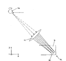
图1是表示作为本发明的一个实施方式的脆性材料基板的倒角加工装置的结构的图。FIG. 1 is a diagram showing the configuration of a chamfering device for a brittle material substrate as one embodiment of the present invention.
图2是图1的扫描光学系统的放大图。FIG. 2 is an enlarged view of the scanning optical system of FIG. 1 .
图3是图1的倒角加工装置的控制系统的框图。Fig. 3 is a block diagram of a control system of the chamfering device of Fig. 1 .
图4是表示形成较深的倒角加工面的情况下的步骤的图。Fig. 4 is a diagram showing a procedure for forming a deep chamfered surface.
图5是扫描光学系统的变形例的放大图。FIG. 5 is an enlarged view of a modified example of the scanning optical system.
图6是扫描光学系统的变形例的放大图。FIG. 6 is an enlarged view of a modified example of the scanning optical system.
图7是扫描光学系统的变形例的放大图。FIG. 7 is an enlarged view of a modified example of the scanning optical system.
图8是表示使用CO2激光光源通过加热熔融法进行倒角加工时的激光照射状态的剖视图。8 is a cross-sectional view showing a state of laser irradiation when chamfering is performed by a heating and melting method using a CO 2 laser light source.
图9是表示使用CO2激光光源通过激光划线法进行倒角加工时的激光照射状态的图。FIG. 9 is a diagram showing a laser irradiation state when chamfering is performed by a laser scribing method using a CO 2 laser light source.
图10是通过利用CO2激光的激光划线法进行倒角加工时的加工剖面的放大图。Fig. 10 is an enlarged view of a processed cross section when chamfering is performed by a laser scribing method using a CO 2 laser.
标号说明Label description
2:滑动工作台;7:基座;11:升降工作台;12:吸附工作台;13:激光光源;14:电流镜(射束偏转部);14a:多面镜;15:凸透镜(聚光部件);15a:fθ透镜;15b:凹面镜;16:扫描光学系统。2: sliding table; 7: base; 11: lifting table; 12: adsorption table; 13: laser light source; 14: current mirror (beam deflection part); 14a: polygonal mirror; 15: convex lens (condensing Component); 15a: fθ lens; 15b: concave mirror; 16: scanning optical system.
具体实施方式Detailed ways
以下,参照附图对本发明的实施方式进行说明。此处,对玻璃基板的倒角加工进行说明。Hereinafter, embodiments of the present invention will be described with reference to the drawings. Here, the chamfering process of a glass substrate is demonstrated.
另外,本发明当然并不限于以下说明的实施方式,在不超出本发明的主旨的范围内包含各种形态。In addition, this invention is not limited to embodiment demonstrated below of course, Various forms are included in the range which does not deviate from the summary of this invention.
图1是表示作为本发明的一个实施方式的脆性材料基板的倒角加工装置LM的图。图2是表示图1的扫描光学系统的放大图。FIG. 1 is a diagram showing a chamfering apparatus LM for a brittle material substrate as one embodiment of the present invention. FIG. 2 is an enlarged view showing the scanning optical system of FIG. 1 .
倒角加工装置LM设有滑动工作台2,该滑动工作台2沿平行配置于水平的架台1上的一对导轨3、4在图1的纸面前后方向(以下称为Y方向)往复移动。在两导轨3、4之间,导螺杆5沿前后方向进行配置,固定于所述滑动工作台2的支柱6螺合于该导螺杆5,通过电动机(未图示)使导螺杆5正转和反转,从而使滑动工作台2沿导轨3、4在Y方向往复移动。The chamfering processing device LM is equipped with a sliding table 2 that reciprocates in the front-back direction (hereinafter referred to as the Y direction) of the paper in FIG. . Between the two guide rails 3, 4, a lead screw 5 is disposed along the front-rear direction, and the pillar 6 fixed to the slide table 2 is screwed to the lead screw 5, and the lead screw 5 is rotated forward by a motor (not shown). And reverse, so that the slide table 2 reciprocates along the guide rails 3, 4 in the Y direction.
在滑动工作台2上,水平的基座7被配置成沿导轨8在图1的左右方向(以下称为X方向)往复移动。在固定于基座7的支柱10a中贯通螺合有通过电动机9进行旋转的导螺杆10,通过导螺杆10正转和反转,基座7沿导轨8在X方向往复移动。On the slide table 2 , a horizontal base 7 is disposed so as to reciprocate along the guide rail 8 in the left-right direction in FIG. 1 (hereinafter referred to as the X direction). A
在基座7上,设有进行高度方向(以下称为Z方向)的调整的升降工作台11、及搭载有吸引卡盘的吸附工作台12,玻璃基板G以水平的状态被设置于该吸附工作台12上。此时,玻璃基板G以包含进行倒角加工的边缘线的基板的那一部分突出于吸附工作台12的外侧的状态被吸附。因此,以进行倒角加工的边缘线EL朝向下方露出的状态进行支撑。On the base 7, there are provided an elevating table 11 for adjustment in the height direction (hereinafter referred to as the Z direction), and an adsorption table 12 on which a suction chuck is mounted, and the glass substrate G is placed on the suction table in a horizontal state. Workbench 12. At this time, the glass substrate G is suctioned in a state in which a part of the substrate including the edge line to be chamfered protrudes from the outside of the suction stage 12 . Therefore, it is supported in a state where the chamfered edge line EL is exposed downward.
此外,玻璃基板G利用摄像机20和在基板上形成的对准标记(未图示)进行定位,并使边缘线EL朝向Y方向。在基板G一定的情况下,也可以预先将定位用的引导件设于吸附工作台12表面,以使基板的一部分与引导件抵接的方式进行定位。Moreover, the glass substrate G is positioned by the camera 20 and the alignment mark (not shown) formed in the board|substrate, and edge line EL faces a Y direction. When the substrate G is constant, positioning guides may be provided on the surface of the suction table 12 in advance, and the positioning may be performed so that a part of the substrate comes into contact with the guides.
在玻璃基板G的上方安装有激光光源13、电流镜14(射束偏转部)、以及凸透镜15(聚光部件)。电流镜14与凸透镜15构成扫描光学系统16。Above the glass substrate G are mounted a laser light source 13 , a galvano mirror 14 (beam deflection unit), and a convex lens 15 (light condensing member). The
激光光源13采用Nd-YAG激光光源。激光光源13在XZ面内,且射出方向为向左下方倾斜45度。The laser light source 13 is a Nd-YAG laser light source. The laser light source 13 is in the XZ plane, and the emission direction is inclined 45 degrees to the lower left.
电流镜14将反射镜配置于从激光光源13射出的激光束的光路上,使激光束向右下方倾斜射出,并通过反射镜的摆动运动,使射束的射出方向在XZ面内偏转。此时的电流镜14的摆动运动的范围依据对加工对象物进行倒角加工的角度范围来调整。The
凸透镜15将从电流镜14射出的激光束聚光,形成会聚点。另外,激光束的强度等被设定成在形成于加工对象物的会聚点处产生多光子吸收。此外,通过电流镜14使射出方向偏转,并扫描激光束向凸透镜15入射的入射位置,其结果是,从凸透镜15射出的激光束的会聚点在XZ面内(亦即,与边缘线EL正交的面内)被扫描到,扫描轨迹朝向光束的行进方向呈凸状。The
例如,如图2所示,通过电流镜14的摆动运动,会聚点的扫描轨迹形成为连结F0、F1、F2的弧R0。For example, as shown in FIG. 2 , by the oscillating motion of the
由于通过电流镜14和凸透镜15形成的会聚点的位置和会聚点的扫描轨迹为一定的位置及轨迹,因此可预先通过几何计算(或实测)求出表示会聚点的坐标(F0,F1,F2的坐标)、轨迹(弧R0)的函数。Because the position of the converging point formed by the
因此,在设置好玻璃基板G之后,通过对滑动工作台2、基座7以及升降工作台11进行XYZ方向的位置调整,使会聚点F0对准在边缘线EL上或边缘线EL附近设定的加工预定面的位置。Therefore, after the glass substrate G is installed, the position of the sliding table 2, the base 7, and the lifting table 11 in the XYZ direction is adjusted so that the point of convergence F0 is set on or near the edge line EL. The position of the processing scheduled surface.
接着,对倒角加工装置LM的控制系统进行说明。图3是控制系统的框图。倒角加工装置LM具备控制部50,该控制部50由用于存储各种控制数据、设定参数及程序(软件)的存储器及用于执行运算处理的CPU构成。Next, the control system of the chamfering processing apparatus LM is demonstrated. Fig. 3 is a block diagram of the control system. The chamfering processing apparatus LM is provided with the
该控制部50控制以下各驱动系统:工作台驱动部51,所述工作台驱动部51驱动用于进行滑动工作台2、基座7的定位、移动的电动机(电动机9等);吸附机构驱动部52,所述吸附机构驱动部52驱动吸附工作台12的吸引卡盘;射束偏转部驱动部53,所述射束偏转部驱动部53驱动电流镜14;以及激光驱动部54,所述激光驱动部54进行激光照射。此外,控制部50连接有由键盘、鼠标等构成的输入部56、以及在显示屏幕上进行各种显示的显示部57,并形成为能够在屏幕上显示必要的信息,且能够输入必要的指令、设定。The
接下来,对倒角加工装置LM的倒角动作进行说明。将基板G装载于吸附工作台12,并使用摄像机20进行位置调整。接着,使边缘线EL朝向Y方向,并且利用滑动工作台2、基座7、升降工作台11进行位置调整,以使会聚点F0的坐标到达边缘线EL上或边缘线EL附近的加工预定面的深度。Next, the chamfering operation of the chamfering processing device LM will be described. The substrate G is placed on the suction table 12 and its position is adjusted using the camera 20 . Next, make the edge line EL face the Y direction, and use the sliding table 2, the base 7, and the elevating table 11 to adjust the position so that the coordinates of the convergence point F0 reach the processing plan surface on or near the edge line EL depth.
接着,驱动电流镜14和激光光源13,使激光束在边缘线附近扫描。其结果是,会聚点通过消融来熔融除去基板材料,形成倒角加工面。Next, the
另外,在边缘线EL的全长范围内进行倒角时,以一定速度移送滑动工作台2,使基板G相对于激光束的扫描面(XZ面)向Y方向移动。此时,也可以间歇地移送滑动工作台2,以使激光束对同一加工位置进行多次扫描。In addition, when chamfering over the entire length of the edge line EL, the slide table 2 is transferred at a constant speed, and the substrate G is moved in the Y direction with respect to the scanning plane (XZ plane) of the laser beam. At this time, the slide table 2 may be moved intermittently so that the laser beam scans the same processing position a plurality of times.
此外,在形成较深的倒角加工面的情况下,分成多次进行倒角加工。亦即,如图4所示,第一次的倒角加工将会聚点设定于接近边缘线EL的较浅位置,并在向Y方向移动的同时进行加工,第二次以后的倒角加工则使会聚点的位置逐渐向基板内部侧移位,并重复进行同样的加工。In addition, when forming a deep chamfered surface, the chamfering process is divided into multiple times. That is, as shown in FIG. 4, the first chamfering process sets the converging point at a shallower position close to the edge line EL, and performs processing while moving in the Y direction, and the second and subsequent chamfering processes Then, the position of the converging point is gradually shifted toward the inner side of the substrate, and the same processing is repeated.
接下来,对变形实施例进行说明。Next, modified examples will be described.
图5是以fθ透镜15a取代凸透镜15作为聚光部件时的扫描光学系统的放大图。在该情况下,由于会聚点的扫描轨迹在XZ面呈直线状,因此能够进行斜面的倒角加工。FIG. 5 is an enlarged view of the scanning optical system when
此外,如果适当地设计透镜的曲面形状、曲率半径、折射率等光学参数,能够制作出可描绘预期的扫描轨迹的自由曲面透镜,因此利用该自由曲面透镜,也能够将倒角加工面形成为抛物面、椭圆面、或任意的自由曲面。再有,采用反射镜取代透镜也能够描绘与透镜的扫描轨迹相同的轨迹。In addition, if the optical parameters such as the shape of the curved surface, radius of curvature, and refractive index of the lens are properly designed, a free-form surface lens that can describe the expected scanning trajectory can be produced. Therefore, the chamfered surface can also be formed by using the free-form surface lens. Paraboloid, ellipse, or any free-form surface. In addition, it is also possible to draw the same trajectory as the scanning trajectory of the lens by using a mirror instead of the lens.
图6是以多面镜14a取代电流镜14作为射束偏转部时的扫描光学系统的放大图。图7是以凹面镜15b来取代透镜作为聚光部件时的扫描光学系统的放大图。在使用这些扫描光学系统的情况下,也能够进行与图2相同的倒角加工。FIG. 6 is an enlarged view of the scanning optical system when the
此外,在沿边缘线EL进行倒角加工时,在图2的倒角加工装置LM中,虽是移动了装载基板G的滑动工作台2,不过也可以移动扫描光学系统(电流镜14、凸透镜15)侧。In addition, when performing chamfering processing along the edge line EL, in the chamfering processing device LM of FIG. 15) Side.
以上,虽然对玻璃基板的倒角加工作了说明,不过对于其它脆性材料基板,通过根据各种脆性材料基板的基板材料的吸收特性选择可使用的激光光源,也能够实现相同的倒角加工。Although the chamfering process of the glass substrate has been described above, the same chamfering process can also be realized for other brittle material substrates by selecting an applicable laser light source according to the absorption characteristics of the substrate material of each brittle material substrate.
产业上的可利用性Industrial availability
本发明可用于玻璃基板等脆性材料基板的倒角加工。The invention can be used for chamfering processing of brittle material substrates such as glass substrates.
Claims (12)
Applications Claiming Priority (3)
| Application Number | Priority Date | Filing Date | Title |
|---|---|---|---|
| JP2007-327599 | 2007-12-19 | ||
| JP2007327599 | 2007-12-19 | ||
| PCT/JP2008/072471 WO2009078324A1 (en) | 2007-12-19 | 2008-12-11 | Method for chamfering/machining brittle material substrate and chamfering/machining apparatus |
Publications (2)
| Publication Number | Publication Date |
|---|---|
| CN101903128A true CN101903128A (en) | 2010-12-01 |
| CN101903128B CN101903128B (en) | 2013-07-17 |
Family
ID=40795440
Family Applications (1)
| Application Number | Title | Priority Date | Filing Date |
|---|---|---|---|
| CN2008801215041A Expired - Fee Related CN101903128B (en) | 2007-12-19 | 2008-12-11 | Method for chamfering/machining brittle material substrate and chamfering/machining apparatus |
Country Status (6)
| Country | Link |
|---|---|
| EP (1) | EP2239085A4 (en) |
| JP (1) | JP5102846B2 (en) |
| KR (1) | KR101183865B1 (en) |
| CN (1) | CN101903128B (en) |
| TW (1) | TW200936290A (en) |
| WO (1) | WO2009078324A1 (en) |
Cited By (9)
| Publication number | Priority date | Publication date | Assignee | Title |
|---|---|---|---|---|
| CN104093673A (en) * | 2012-01-09 | 2014-10-08 | 拉米耐克斯株式会社 | Method and apparatus for processing edge of glass plate |
| CN106552996A (en) * | 2015-09-24 | 2017-04-05 | 武汉吉事达激光设备有限公司 | Glass laser chamfering method and equipment |
| CN107530833A (en) * | 2015-06-02 | 2018-01-02 | 川崎重工业株式会社 | Chamfer processing method and device and chamfer processing method |
| CN110655316A (en) * | 2018-06-29 | 2020-01-07 | 三星钻石工业股份有限公司 | Substrate dividing method and dividing device |
| CN111843216A (en) * | 2020-07-22 | 2020-10-30 | 江苏亚威艾欧斯激光科技有限公司 | Glass substrate side processing device and processing method thereof |
| CN111974852A (en) * | 2020-07-09 | 2020-11-24 | 中船第九设计研究院工程有限公司 | Chamfering process in ship T-shaped material production process |
| CN113894410A (en) * | 2020-06-22 | 2022-01-07 | 三星显示有限公司 | Laser processing apparatus |
| CN117260016A (en) * | 2023-10-31 | 2023-12-22 | 浙江华工光润智能装备技术有限公司 | Chamfer processing device and processing method |
| CN118848282A (en) * | 2024-09-03 | 2024-10-29 | 嘉兴艾可镭光电科技有限公司 | A multifunctional wafer picosecond laser processing device and its use method |
Families Citing this family (8)
| Publication number | Priority date | Publication date | Assignee | Title |
|---|---|---|---|---|
| CN101987554B (en) * | 2009-08-07 | 2013-04-17 | 深圳市大族激光科技股份有限公司 | Laser engraving device |
| KR101181719B1 (en) * | 2010-06-22 | 2012-09-19 | 한국과학기술원 | Substrate Dicing Method by Nano Void Array Formation using Femtosecond Pulse Lasers |
| KR101574934B1 (en) * | 2014-05-27 | 2015-12-08 | 로체 시스템즈(주) | Chamfering method for brittle material |
| JP6303950B2 (en) * | 2014-09-19 | 2018-04-04 | 旭硝子株式会社 | Glass plate processing method |
| JP7094946B2 (en) * | 2016-09-29 | 2022-07-04 | コーニング インコーポレイテッド | Changing the composition of glass articles by laser heating and its manufacturing method |
| CN110757006B (en) * | 2019-10-23 | 2022-06-03 | 武汉数字化设计与制造创新中心有限公司 | Photovoltaic glass through hole laser chamfering device and method |
| JP6932865B1 (en) * | 2021-03-19 | 2021-09-08 | 株式会社東京精密 | Reformer and reformer method for wafer edge |
| JP7221345B2 (en) * | 2021-03-19 | 2023-02-13 | 株式会社東京精密 | Wafer edge modification apparatus and modification method |
Citations (6)
| Publication number | Priority date | Publication date | Assignee | Title |
|---|---|---|---|---|
| JPH02241684A (en) * | 1989-03-13 | 1990-09-26 | Tokai Rika Co Ltd | Method for chamfering glass member |
| JPH09225665A (en) * | 1996-02-22 | 1997-09-02 | Seiko Epson Corp | Glass substrate chamfering method, glass substrate for liquid crystal panel and liquid crystal panel using the method |
| CN1491144A (en) * | 2001-08-10 | 2004-04-21 | 三星钻石工业股份有限公司 | Chamfering method and chamfering device for brittle material substrate |
| JP2006263810A (en) * | 2005-02-28 | 2006-10-05 | Sunx Ltd | Laser beam machining method and apparatus |
| JP2007245235A (en) * | 2006-02-14 | 2007-09-27 | Shibaura Mechatronics Corp | Laser processing apparatus and laser processing method |
| JP2007319881A (en) * | 2006-05-31 | 2007-12-13 | Seiko Epson Corp | Substrate manufacturing method, laser processing device, display device, electro-optical device, electronic device |
Family Cites Families (3)
| Publication number | Priority date | Publication date | Assignee | Title |
|---|---|---|---|---|
| US6191382B1 (en) * | 1998-04-02 | 2001-02-20 | Avery Dennison Corporation | Dynamic laser cutting apparatus |
| JP2005178288A (en) * | 2003-12-22 | 2005-07-07 | Shibuya Kogyo Co Ltd | Method and device for cutting brittle material |
| JP4407584B2 (en) * | 2005-07-20 | 2010-02-03 | セイコーエプソン株式会社 | Laser irradiation apparatus and laser scribing method |
-
2008
- 2008-12-11 KR KR1020107012767A patent/KR101183865B1/en not_active Expired - Fee Related
- 2008-12-11 CN CN2008801215041A patent/CN101903128B/en not_active Expired - Fee Related
- 2008-12-11 JP JP2009546230A patent/JP5102846B2/en not_active Expired - Fee Related
- 2008-12-11 WO PCT/JP2008/072471 patent/WO2009078324A1/en not_active Ceased
- 2008-12-11 EP EP08862224.6A patent/EP2239085A4/en not_active Withdrawn
- 2008-12-17 TW TW097149120A patent/TW200936290A/en not_active IP Right Cessation
Patent Citations (6)
| Publication number | Priority date | Publication date | Assignee | Title |
|---|---|---|---|---|
| JPH02241684A (en) * | 1989-03-13 | 1990-09-26 | Tokai Rika Co Ltd | Method for chamfering glass member |
| JPH09225665A (en) * | 1996-02-22 | 1997-09-02 | Seiko Epson Corp | Glass substrate chamfering method, glass substrate for liquid crystal panel and liquid crystal panel using the method |
| CN1491144A (en) * | 2001-08-10 | 2004-04-21 | 三星钻石工业股份有限公司 | Chamfering method and chamfering device for brittle material substrate |
| JP2006263810A (en) * | 2005-02-28 | 2006-10-05 | Sunx Ltd | Laser beam machining method and apparatus |
| JP2007245235A (en) * | 2006-02-14 | 2007-09-27 | Shibaura Mechatronics Corp | Laser processing apparatus and laser processing method |
| JP2007319881A (en) * | 2006-05-31 | 2007-12-13 | Seiko Epson Corp | Substrate manufacturing method, laser processing device, display device, electro-optical device, electronic device |
Cited By (10)
| Publication number | Priority date | Publication date | Assignee | Title |
|---|---|---|---|---|
| CN104093673A (en) * | 2012-01-09 | 2014-10-08 | 拉米耐克斯株式会社 | Method and apparatus for processing edge of glass plate |
| CN107530833A (en) * | 2015-06-02 | 2018-01-02 | 川崎重工业株式会社 | Chamfer processing method and device and chamfer processing method |
| CN107530833B (en) * | 2015-06-02 | 2018-12-07 | 川崎重工业株式会社 | Chamfer processing method and device and chamfer processing method |
| CN106552996A (en) * | 2015-09-24 | 2017-04-05 | 武汉吉事达激光设备有限公司 | Glass laser chamfering method and equipment |
| CN110655316A (en) * | 2018-06-29 | 2020-01-07 | 三星钻石工业股份有限公司 | Substrate dividing method and dividing device |
| CN113894410A (en) * | 2020-06-22 | 2022-01-07 | 三星显示有限公司 | Laser processing apparatus |
| CN111974852A (en) * | 2020-07-09 | 2020-11-24 | 中船第九设计研究院工程有限公司 | Chamfering process in ship T-shaped material production process |
| CN111843216A (en) * | 2020-07-22 | 2020-10-30 | 江苏亚威艾欧斯激光科技有限公司 | Glass substrate side processing device and processing method thereof |
| CN117260016A (en) * | 2023-10-31 | 2023-12-22 | 浙江华工光润智能装备技术有限公司 | Chamfer processing device and processing method |
| CN118848282A (en) * | 2024-09-03 | 2024-10-29 | 嘉兴艾可镭光电科技有限公司 | A multifunctional wafer picosecond laser processing device and its use method |
Also Published As
| Publication number | Publication date |
|---|---|
| JP5102846B2 (en) | 2012-12-19 |
| JPWO2009078324A1 (en) | 2011-04-28 |
| EP2239085A4 (en) | 2016-12-14 |
| TW200936290A (en) | 2009-09-01 |
| KR101183865B1 (en) | 2012-09-19 |
| KR20100087371A (en) | 2010-08-04 |
| EP2239085A1 (en) | 2010-10-13 |
| WO2009078324A1 (en) | 2009-06-25 |
| CN101903128B (en) | 2013-07-17 |
| TWI361741B (en) | 2012-04-11 |
Similar Documents
| Publication | Publication Date | Title |
|---|---|---|
| CN101903128B (en) | Method for chamfering/machining brittle material substrate and chamfering/machining apparatus | |
| CN102123817B (en) | Decorner processing device | |
| CN101386467B (en) | Method and device for dividing brittle substrate | |
| CN1283409C (en) | Brittle material substrate chamfering method and chamfering device | |
| JP5113462B2 (en) | Method for chamfering a brittle material substrate | |
| KR101398288B1 (en) | Splitting method of processed object and splitting method of substrate having optical element pattern | |
| WO2006070825A1 (en) | Method for cutting brittle material substrate and substrate cutting system | |
| CN1264768C (en) | Device and method for scribing fragile material substrate | |
| JP4776911B2 (en) | Laser processing apparatus and laser processing method | |
| JP2011230940A (en) | Cutting method for brittle material substrate | |
| JP4134033B2 (en) | Scribing apparatus and scribing method for brittle material substrate | |
| KR100551527B1 (en) | Scribing method and scribing apparatus for brittle material substrate | |
| TWI475710B (en) | Device for the production of thin layer solar cell module | |
| JP5444158B2 (en) | Cleaving method of brittle material substrate | |
| JP5887927B2 (en) | Cutting device |
Legal Events
| Date | Code | Title | Description |
|---|---|---|---|
| C06 | Publication | ||
| PB01 | Publication | ||
| C10 | Entry into substantive examination | ||
| SE01 | Entry into force of request for substantive examination | ||
| C14 | Grant of patent or utility model | ||
| GR01 | Patent grant | ||
| CF01 | Termination of patent right due to non-payment of annual fee |
Granted publication date: 20130717 Termination date: 20171211 |
|
| CF01 | Termination of patent right due to non-payment of annual fee |