CN101874289A - Method for manufacturing semiconductor device and semiconductor device - Google Patents
Method for manufacturing semiconductor device and semiconductor device Download PDFInfo
- Publication number
- CN101874289A CN101874289A CN200880117656A CN200880117656A CN101874289A CN 101874289 A CN101874289 A CN 101874289A CN 200880117656 A CN200880117656 A CN 200880117656A CN 200880117656 A CN200880117656 A CN 200880117656A CN 101874289 A CN101874289 A CN 101874289A
- Authority
- CN
- China
- Prior art keywords
- film
- substrate
- thin
- semiconductor
- semiconductor device
- Prior art date
- Legal status (The legal status is an assumption and is not a legal conclusion. Google has not performed a legal analysis and makes no representation as to the accuracy of the status listed.)
- Granted
Links
Images




Classifications
-
- G—PHYSICS
- G02—OPTICS
- G02F—OPTICAL DEVICES OR ARRANGEMENTS FOR THE CONTROL OF LIGHT BY MODIFICATION OF THE OPTICAL PROPERTIES OF THE MEDIA OF THE ELEMENTS INVOLVED THEREIN; NON-LINEAR OPTICS; FREQUENCY-CHANGING OF LIGHT; OPTICAL LOGIC ELEMENTS; OPTICAL ANALOGUE/DIGITAL CONVERTERS
- G02F1/00—Devices or arrangements for the control of the intensity, colour, phase, polarisation or direction of light arriving from an independent light source, e.g. switching, gating or modulating; Non-linear optics
- G02F1/01—Devices or arrangements for the control of the intensity, colour, phase, polarisation or direction of light arriving from an independent light source, e.g. switching, gating or modulating; Non-linear optics for the control of the intensity, phase, polarisation or colour
- G02F1/13—Devices or arrangements for the control of the intensity, colour, phase, polarisation or direction of light arriving from an independent light source, e.g. switching, gating or modulating; Non-linear optics for the control of the intensity, phase, polarisation or colour based on liquid crystals, e.g. single liquid crystal display cells
- G02F1/133—Constructional arrangements; Operation of liquid crystal cells; Circuit arrangements
- G02F1/1333—Constructional arrangements; Manufacturing methods
- G02F1/1345—Conductors connecting electrodes to cell terminals
- G02F1/13454—Drivers integrated on the active matrix substrate
-
- H—ELECTRICITY
- H10—SEMICONDUCTOR DEVICES; ELECTRIC SOLID-STATE DEVICES NOT OTHERWISE PROVIDED FOR
- H10D—INORGANIC ELECTRIC SEMICONDUCTOR DEVICES
- H10D86/00—Integrated devices formed in or on insulating or conducting substrates, e.g. formed in silicon-on-insulator [SOI] substrates or on stainless steel or glass substrates
- H10D86/01—Manufacture or treatment
- H10D86/021—Manufacture or treatment of multiple TFTs
- H10D86/0214—Manufacture or treatment of multiple TFTs using temporary substrates
-
- H—ELECTRICITY
- H10—SEMICONDUCTOR DEVICES; ELECTRIC SOLID-STATE DEVICES NOT OTHERWISE PROVIDED FOR
- H10D—INORGANIC ELECTRIC SEMICONDUCTOR DEVICES
- H10D86/00—Integrated devices formed in or on insulating or conducting substrates, e.g. formed in silicon-on-insulator [SOI] substrates or on stainless steel or glass substrates
- H10D86/40—Integrated devices formed in or on insulating or conducting substrates, e.g. formed in silicon-on-insulator [SOI] substrates or on stainless steel or glass substrates characterised by multiple TFTs
- H10D86/421—Integrated devices formed in or on insulating or conducting substrates, e.g. formed in silicon-on-insulator [SOI] substrates or on stainless steel or glass substrates characterised by multiple TFTs having a particular composition, shape or crystalline structure of the active layer
- H10D86/425—Integrated devices formed in or on insulating or conducting substrates, e.g. formed in silicon-on-insulator [SOI] substrates or on stainless steel or glass substrates characterised by multiple TFTs having a particular composition, shape or crystalline structure of the active layer having different crystal properties in different TFTs or within an individual TFT
-
- H—ELECTRICITY
- H10—SEMICONDUCTOR DEVICES; ELECTRIC SOLID-STATE DEVICES NOT OTHERWISE PROVIDED FOR
- H10D—INORGANIC ELECTRIC SEMICONDUCTOR DEVICES
- H10D86/00—Integrated devices formed in or on insulating or conducting substrates, e.g. formed in silicon-on-insulator [SOI] substrates or on stainless steel or glass substrates
- H10D86/40—Integrated devices formed in or on insulating or conducting substrates, e.g. formed in silicon-on-insulator [SOI] substrates or on stainless steel or glass substrates characterised by multiple TFTs
- H10D86/471—Integrated devices formed in or on insulating or conducting substrates, e.g. formed in silicon-on-insulator [SOI] substrates or on stainless steel or glass substrates characterised by multiple TFTs having different architectures, e.g. having both top-gate and bottom-gate TFTs
-
- H—ELECTRICITY
- H10—SEMICONDUCTOR DEVICES; ELECTRIC SOLID-STATE DEVICES NOT OTHERWISE PROVIDED FOR
- H10D—INORGANIC ELECTRIC SEMICONDUCTOR DEVICES
- H10D86/00—Integrated devices formed in or on insulating or conducting substrates, e.g. formed in silicon-on-insulator [SOI] substrates or on stainless steel or glass substrates
- H10D86/40—Integrated devices formed in or on insulating or conducting substrates, e.g. formed in silicon-on-insulator [SOI] substrates or on stainless steel or glass substrates characterised by multiple TFTs
- H10D86/60—Integrated devices formed in or on insulating or conducting substrates, e.g. formed in silicon-on-insulator [SOI] substrates or on stainless steel or glass substrates characterised by multiple TFTs wherein the TFTs are in active matrices
-
- H—ELECTRICITY
- H10—SEMICONDUCTOR DEVICES; ELECTRIC SOLID-STATE DEVICES NOT OTHERWISE PROVIDED FOR
- H10D—INORGANIC ELECTRIC SEMICONDUCTOR DEVICES
- H10D30/00—Field-effect transistors [FET]
- H10D30/01—Manufacture or treatment
- H10D30/021—Manufacture or treatment of FETs having insulated gates [IGFET]
- H10D30/031—Manufacture or treatment of FETs having insulated gates [IGFET] of thin-film transistors [TFT]
- H10D30/0321—Manufacture or treatment of FETs having insulated gates [IGFET] of thin-film transistors [TFT] comprising silicon, e.g. amorphous silicon or polysilicon
- H10D30/0323—Manufacture or treatment of FETs having insulated gates [IGFET] of thin-film transistors [TFT] comprising silicon, e.g. amorphous silicon or polysilicon comprising monocrystalline silicon
Landscapes
- Physics & Mathematics (AREA)
- Nonlinear Science (AREA)
- Mathematical Physics (AREA)
- Chemical & Material Sciences (AREA)
- Crystallography & Structural Chemistry (AREA)
- General Physics & Mathematics (AREA)
- Optics & Photonics (AREA)
- Thin Film Transistor (AREA)
Abstract
本发明公开了一种半导体装置的制造方法以及半导体装置。该半导体装置的制造方法是制造包括具有薄膜晶体管的薄膜器件部和设置在薄膜器件部的周围并具有半导体元件的周围器件部的半导体装置的方法,包括:准备基板的第一步骤、在基板上直接贴合周围器件部的第二步骤以及在已贴合了周围器件部的基板上形成薄膜器件部的第三步骤。

The present invention discloses a method for manufacturing a semiconductor device and a semiconductor device. The method is a method for manufacturing a semiconductor device including a thin-film device portion having a thin-film transistor and a peripheral device portion disposed around the thin-film device portion and having a semiconductor element, comprising: a first step of preparing a substrate; a second step of directly attaching the peripheral device portion to the substrate; and a third step of forming the thin-film device portion on the substrate to which the peripheral device portion has been attached.
Description
技术领域technical field
本发明涉及一种半导体装置的制造方法及半导体装置。The present invention relates to a method for manufacturing a semiconductor device and the semiconductor device.
背景技术Background technique
近年来,作为与显示装置相关的技术,将驱动电路部、控制电路部等周围器件部和像素部一体化的液晶显示器、即所谓的单片式液晶显示器(下面,也称作“系统液晶”)正受到关注。在用于这种系统液晶的半导体装置中,因为在同一基板上同时形成像素部的开关元件和周围器件部,所以能够大幅度减少部件数量。还有,能够削减液晶显示器的组装工序及检验工序。为此,既能降低制造成本,又能提高可靠性。In recent years, as technologies related to display devices, a so-called single-chip liquid crystal display (hereinafter, also referred to as "system liquid crystal") is a liquid crystal display in which peripheral devices such as a driver circuit unit and a control circuit unit are integrated with a pixel unit. ) is receiving attention. In the semiconductor device used for such a system liquid crystal, since the switching element of the pixel portion and the peripheral device portion are simultaneously formed on the same substrate, the number of components can be significantly reduced. In addition, the assembly process and inspection process of the liquid crystal display can be reduced. For this reason, the manufacturing cost can be reduced and the reliability can be improved.
对液晶显示装置等显示装置实现低耗电化、图像显示的高精细化和高速化等高性能化的要求日趋迫切。还要求周围器件部实现省空间化,进而要求实现高度的系统(存储器、信号处理电路等)集成化。Display devices such as liquid crystal display devices are increasingly required to achieve high performance such as low power consumption, high-definition and high-speed image display. It is also required to realize space-saving of peripheral device parts, and further, to realize a high degree of system (memory, signal processing circuit, etc.) integration.
为此,对用于显示装置中的半导体装置,提出了使各个元件进一步实现精细化的迫切要求,为了在有限的面积中形成多个元件,就要求周围器件部要达到亚微米级的设计规则、即集成电路(下面,也称作“IC”)级的微细图案精度。还有,对构成周围器件部的半导体元件,提出了提高半导体层中的载流子迁移率的要求,为了实现这一要求,也需要实现元件的精细化。For this reason, for semiconductor devices used in display devices, there is an urgent demand for further refinement of each element. In order to form a plurality of elements in a limited area, it is required that the surrounding device parts should achieve sub-micron level design rules. , That is, the fine pattern accuracy of the integrated circuit (hereinafter, also referred to as "IC") level. In addition, semiconductor elements constituting the peripheral device portion are required to increase carrier mobility in the semiconductor layer, and in order to realize this requirement, it is also necessary to refine the elements.
不过,在玻璃基板上直接形成半导体装置的原有制造工艺中,因为玻璃基板的耐热性较低,所以在制造工艺的热处理工序中有可能导致玻璃基板产生翘曲变形,因而有时无法形成所希望的亚微米级电路图案。还有,用于制造系统液晶等液晶显示装置的玻璃基板正不断地趋向大型化,因而在制造工艺中更容易产生玻璃基板面内的翘曲变形。However, in the conventional manufacturing process of directly forming a semiconductor device on a glass substrate, because the heat resistance of the glass substrate is low, the glass substrate may be warped and deformed during the heat treatment process of the manufacturing process. Desired sub-micron circuit patterning. In addition, glass substrates used in the manufacture of liquid crystal display devices such as system liquid crystals are constantly increasing in size, so in-plane warpage of the glass substrate is more likely to occur during the manufacturing process.
对此,开发出一种使用在设于电绝缘物上的单晶硅层形成有集成电路的SOI(Silicon On Insulator,绝缘体上硅)基板,向液晶显示器的基板上转印周围器件部的技术。根据该技术,因为能够使用原有的IC芯片制作工序形成包含半导体元件的集成电路,所以能够实现包括具有所希望的亚微米级电路设计的微细且高性能的集成电路的半导体装置。但是,在向基板上转印周围器件部时,如果不是在使基板成为平坦的状态下进行转印的话,就很难确实地将周围器件部接合到基板上。In response to this, a technology has been developed to transfer peripheral device parts onto the substrate of a liquid crystal display using an SOI (Silicon On Insulator, silicon-on-insulator) substrate on which an integrated circuit is formed on a single crystal silicon layer provided on an electrical insulator. . According to this technology, since an integrated circuit including a semiconductor element can be formed using an existing IC chip manufacturing process, a semiconductor device including a fine and high-performance integrated circuit having a desired submicron circuit design can be realized. However, when the peripheral device portion is transferred onto the substrate, it is difficult to securely bond the peripheral device portion to the substrate unless the transfer is performed with the substrate flat.
针对这样的问题,研究并开发出一种技术,即:例如,像专利文献1所公开的那样,在形成像素部的栅极电极后,利用蚀刻去除要用来设置周围器件部的区域的绝缘膜和牺牲膜,将具有半导体元件的半导体器件接合到该区域上。根据该技术,在去除牺牲膜时,通过利用选择比与玻璃基板相适合的蚀刻溶液进行蚀刻,就能够降低玻璃表面的微粗糙度。还有,能够认为:与未形成牺牲膜的工艺(仅蚀刻去除绝缘膜,使玻璃表面露出)相比,转印后的接合性良好。In response to such a problem, a technique has been researched and developed in which, for example, as disclosed in Patent Document 1, after forming the gate electrode of the pixel portion, etching is used to remove the insulation of the region where the peripheral device portion is to be provided. film and a sacrificial film, and a semiconductor device having a semiconductor element is bonded to this region. According to this technique, when removing the sacrificial film, the microroughness of the glass surface can be reduced by etching with an etching solution having a selective ratio suitable for the glass substrate. In addition, it can be considered that the adhesiveness after transfer is better than the process in which no sacrificial film is formed (only the insulating film is etched away to expose the glass surface).
专利文献1:日本公开特许公报特开2004-158821号公报Patent Document 1: Japanese Laid-Open Patent Publication No. 2004-158821
发明内容Contents of the invention
发明要解决的问题The problem to be solved by the invention
不过,在如上所述形成像素部的栅极电极后,利用蚀刻去除要用来设置周围器件部的区域的绝缘膜和牺牲膜,将具有半导体元件的半导体器件接合到该区域上的方法中,必须要具有形成牺牲膜的工序,因而在制造效率上存在问题。还有,在蚀刻以后,由于在玻璃表面残留的牺牲膜的残渣等以及因热处理引起的玻璃基板的翘曲变形,而有可能对玻璃基板和周围器件部之间的接合性造成不良影响。However, in the method of bonding a semiconductor device having a semiconductor element to this region after forming the gate electrode of the pixel portion as described above, removing the insulating film and the sacrificial film by etching the region where the peripheral device portion is to be provided, Since a step of forming a sacrificial film is necessary, there is a problem in production efficiency. In addition, after etching, residues of the sacrificial film remaining on the glass surface and warpage of the glass substrate due to heat treatment may adversely affect the bondability between the glass substrate and surrounding device parts.
用于解决问题的方案solutions to problems
本发明正是鉴于所述问题而发明出来的,其目的在于:提供一种制造效率高且基板和周围器件部之间的接合性良好的半导体装置的制造方法及半导体装置。The present invention was conceived in view of the above problems, and an object of the present invention is to provide a method of manufacturing a semiconductor device and a semiconductor device with high manufacturing efficiency and good bonding between a substrate and a peripheral device portion.
本发明所涉及的半导体装置的制造方法是制造包括具有显示元件的薄膜器件部和设置在该薄膜器件部的周围并具有半导体元件的周围器件部的半导体装置的方法,其特征在于:包括准备玻璃基板的第一步骤、在玻璃基板上直接贴合周围器件部的第二步骤以及在已贴合了周围器件部的玻璃基板上形成薄膜器件部的第三步骤。The method for manufacturing a semiconductor device according to the present invention is a method for manufacturing a semiconductor device including a thin film device portion having a display element and a peripheral device portion disposed around the thin film device portion and having a semiconductor element, and is characterized in that it includes preparing a glass The first step of the substrate, the second step of directly bonding the peripheral device part on the glass substrate, and the third step of forming the thin film device part on the glass substrate on which the peripheral device part has been bonded.
还有,本发明所涉及的半导体装置包括具有绝缘表面的基板、设置在基板上的薄膜器件部以及设置在基板上且位于薄膜器件部的周围并具有半导体元件的周围器件部,其特征在于:周围器件部直接设置在基板的绝缘表面上。Also, the semiconductor device related to the present invention includes a substrate having an insulating surface, a thin film device portion disposed on the substrate, and a peripheral device portion disposed on the substrate and positioned around the thin film device portion and having a semiconductor element, characterized in that: The peripheral device portion is disposed directly on the insulating surface of the substrate.
根据这样的构成,因为将周围器件部直接贴合在玻璃基板上,所以在平坦的玻璃基板和周围器件部之间不存在其它膜等。因此,玻璃基板和周围器件部能很好地接合起来。还有,因为没有在玻璃基板上形成牺牲膜等,所以装置的制造效率良好。再有,因为在形成薄膜器件部之前,就将周围器件部贴合在玻璃基板上,所以在贴合周围器件部之前的玻璃基板上不存在牺牲膜等的残渣等,不会产生因热处理等引起的翘曲变形。为此,能够将周围器件部贴在更平坦的玻璃基板的表面上。因此,使玻璃基板和周围器件部更好地接合起来。According to such a configuration, since the peripheral device portion is directly bonded to the glass substrate, no other film or the like is present between the flat glass substrate and the peripheral device portion. Therefore, the glass substrate and the peripheral device portion can be bonded well. Also, since no sacrificial film or the like is formed on the glass substrate, the manufacturing efficiency of the device is good. Furthermore, since the peripheral device portion is bonded to the glass substrate before the thin-film device portion is formed, there is no residue of the sacrificial film or the like on the glass substrate before bonding the peripheral device portion, and there is no risk of damage caused by heat treatment, etc. caused by warping. For this reason, the peripheral device portion can be attached to the surface of the flatter glass substrate. Therefore, the glass substrate and the peripheral device portion are better bonded.
发明效果Invention effect
根据本发明,能够提供一种制造效率高且基板和周围器件部之间的接合性良好的半导体装置的制造方法及半导体装置。According to the present invention, it is possible to provide a method of manufacturing a semiconductor device and a semiconductor device with high manufacturing efficiency and good bonding between a substrate and a peripheral device portion.
附图说明Description of drawings
图1是第一实施方式所涉及的形成有对准标记的玻璃基板的剖视图。FIG. 1 is a cross-sectional view of a glass substrate on which an alignment mark is formed according to a first embodiment.
图2是表示已粘贴上周围器件部的状态的玻璃基板的剖视图。Fig. 2 is a cross-sectional view showing a glass substrate in a state where a peripheral device portion is pasted.
图3是表示已形成了栅极绝缘膜的状态的玻璃基板的剖视图。3 is a cross-sectional view showing a glass substrate in a state where a gate insulating film has been formed.
图4是表示已形成了栅极电极的状态的玻璃基板的剖视图。4 is a cross-sectional view showing a glass substrate in a state where a gate electrode has been formed.
图5是表示已形成了保护膜的状态的玻璃基板的剖视图。5 is a cross-sectional view showing a glass substrate in a state where a protective film has been formed.
图6是表示利用蚀刻去除了显示区域和周围器件部之间的交界部以及周围器件部上的基础包覆层、栅极绝缘膜及保护膜的状态的玻璃基板的剖视图。6 is a cross-sectional view of a glass substrate showing a state in which a boundary portion between a display region and a peripheral device portion and a basic cladding layer, a gate insulating film, and a protective film on the peripheral device portion have been removed by etching.
图7是表示已形成了TEOS(正硅酸乙酯)膜的状态的玻璃基板的剖视图。7 is a cross-sectional view showing a glass substrate in a state where a TEOS (tetraethyl silicate) film has been formed.
图8是表示已形成了接触孔的状态的玻璃基板的剖视图。8 is a cross-sectional view showing a glass substrate in a state where a contact hole has been formed.
图9是第一实施方式所涉及的元件基板的剖视图。9 is a cross-sectional view of the element substrate according to the first embodiment.
图10是第一实施方式所涉及的液晶显示装置的剖视图。10 is a cross-sectional view of the liquid crystal display device according to the first embodiment.
图11是第二实施方式所涉及的形成有对准标记的玻璃基板的剖视图。11 is a cross-sectional view of a glass substrate on which an alignment mark is formed according to a second embodiment.
图12是表示已粘贴上周围器件部的状态的玻璃基板的剖视图。Fig. 12 is a cross-sectional view showing a glass substrate in a state where a peripheral device portion is pasted.
图13是表示已形成了栅极电极的状态的玻璃基板的剖视图。13 is a cross-sectional view showing a glass substrate in a state where a gate electrode has been formed.
图14是表示已形成了SiN(氮化硅)膜的状态的玻璃基板的剖视图。14 is a cross-sectional view showing a glass substrate in a state where a SiN (silicon nitride) film has been formed.
图15是表示已形成了平坦化膜的状态的玻璃基板的剖视图。15 is a cross-sectional view showing a glass substrate in a state where a planarizing film has been formed.
图16是表示已蚀刻了平坦化膜的状态的玻璃基板的剖视图。Fig. 16 is a cross-sectional view showing a glass substrate in a state where a planarizing film has been etched.
图17是第二实施方式所涉及的元件基板的剖视图。17 is a cross-sectional view of an element substrate according to a second embodiment.
附图标记说明:Explanation of reference signs:
10:液晶显示装置;11、111:元件基板;20、120:薄膜器件部;21:TFT(薄膜晶体管);22、122:玻璃基板;23、52:半导体基板;40、140:周围器件部;41、141:对准标记;42:MOS晶体管;160:台阶部;161:平坦化膜;163:金属布线。10: Liquid crystal display device; 11, 111: Element substrate; 20, 120: Thin film device department; 21: TFT (thin film transistor); 22, 122: Glass substrate; 23, 52: Semiconductor substrate; 40, 140: Peripheral device department ; 41, 141: alignment mark; 42: MOS transistor; 160: step portion; 161: planarizing film; 163: metal wiring.
具体实施方式Detailed ways
下面,参照附图对本发明的实施方式进行详细的说明。此外,本发明并不限于以下实施方式。Hereinafter, embodiments of the present invention will be described in detail with reference to the drawings. In addition, the present invention is not limited to the following embodiments.
(第一实施方式)(first embodiment)
图1至图10表示的是本发明的第一实施方式。图10是表示液晶显示装置10的主要部分的示意图。图9是表示元件基板11的主要部分的放大图。还有,图1至图9是对作为半导体装置的元件基板11的制造方法进行说明的剖视图。1 to 10 show a first embodiment of the present invention. FIG. 10 is a schematic diagram showing main parts of a liquid
如图10所示,液晶显示装置10包括元件基板11、与元件基板11相向而设的相对基板12以及形成在这两个基板之间的液晶层13。As shown in FIG. 10 , a liquid
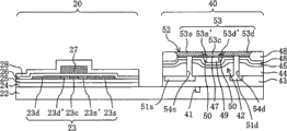
如图9所示,元件基板11包括薄膜器件部20。在元件基板11的薄膜器件部20中,设置有多个像素(省略图示),对应各个像素中的每一个像素形成了作为显示元件的TFT(薄膜晶体管)21。还有,在元件基板11的液晶层13一侧的表面上设置有取向膜14,并且在该元件基板11的与液晶层13相反一侧的表面上层叠有偏光板15。还有,在元件基板11中,用来驱动并控制各个TFT21的周围器件部40设置在薄膜器件部20的周围。As shown in FIG. 9 , the
在相对基板12上,形成有彩色滤光片及由ITO(氧化铟锡)形成的共用电极等,省略它们的图示。还有,在相对基板12的液晶层13一侧的表面上设置有取向膜l6,并且在该相对基板12的与液晶层13相反一侧的表面上层叠有偏光板17。还有,液晶层13由设置在元件基板11和相对基板12之间的密封部件18密封起来。这样一来,液晶显示装置10就利用TFT21控制液晶层13中的液晶分子的取向状态,以进行所希望的显示。A color filter, a common electrode made of ITO (indium tin oxide), and the like are formed on the
TFT21隔着基础包覆层24、25形成在玻璃基板22上。能够适当地用钡-硼硅酸盐玻璃、钡-铝硼硅酸盐玻璃、碱土金属-铝硼硅酸盐玻璃、硼硅酸盐玻璃、碱土金属-锌-铅-铝硼硅酸盐玻璃或者碱土金属-锌-铝硼硅酸盐玻璃等作玻璃基板22。TFT21具有包含活性区域的半导体层23、覆盖半导体层23的栅极绝缘膜26、设置在栅极绝缘膜26上的栅极电极27以及覆盖栅极电极27的保护膜28。半导体层23是由沟道区域23c、形成在沟道区域两侧的LDD(LightlyDoped Drain,轻掺杂漏极)区域23s’、23d’(均为低浓度杂质区域)以及从两侧夹着沟道区域23c及LDD区域23s’、23d’形成的源极区域23s及漏极区域23d(均为高浓度杂质区域)构成的。半导体层23是由非晶硅半导体层或多晶硅半导体层构成的。The
如图9所示,周围器件部40形成在玻璃基板22表面的与对准标记41相对应的位置。周围器件部40具有作为半导体元件的MOS晶体管42。作为第一平坦化膜的绝缘膜43、作为第二平坦化膜的层间绝缘膜44、层间绝缘膜45及绝缘膜46按照这一顺序层叠在玻璃基板22上。绝缘膜43接合在玻璃基板22的表面上。As shown in FIG. 9 , the
周围器件部40中的绝缘膜46的表面朝玻璃基板22一侧凹进去,在该绝缘膜46的表面上形成有栅极氧化膜47和LOCOS(硅的局部氧化)氧化膜48。在栅极氧化膜47和绝缘膜46之间形成有栅极电极49和侧壁50。侧壁50分别形成在栅极电极49的左右两侧的侧面上。The surface of the insulating
在绝缘膜43中,该绝缘膜43与层间绝缘膜44的交界处形成有源极电极51s及漏极电极51d。In the insulating
在栅极氧化膜47的表面上形成有半导体层52,该半导体层52为单晶硅层。半导体层52是这样形成的,即:通过将剥离用物质离子注入到半导体基板中,形成了剥离层后,沿着剥离层分离并去除掉半导体基板的一部分,由此就形成了半导体层52。A
在半导体层52中形成有活性区域53,该活性区域53是由沟道区域53c、形成在该沟道区域左右两侧的LDD区域(低浓度杂质区域)53s’、53d’以及进一步形成在该LDD区域左右两侧的源极区域及漏极区域(高浓度杂质区域)53s、53d构成的。向LDD区域53s’、53d’以及源极区域及漏极区域53s、53d,注入例如磷等N型杂质。An
沟道区域53c是以隔着栅极氧化膜47与栅极电极49相向的方式形成的。还有,LDD区域53s’、53d’是以隔着栅极氧化膜47与侧壁50相向的方式形成的。并且,源极电极51s经由接触孔54s连接在源极区域53s上,另一方面漏极电极51d经由接触孔54d连接在漏极区域53d上。
在TFT21的保护膜28上以及周围器件部40的半导体层52上,分别形成有作为绝缘膜的TEOS膜55、SiN膜56及TEOS膜57。以贯穿TEOS膜55、SiN膜56、TEOS膜57、保护膜28及栅极绝缘膜26后分别到达半导体层23的源极区域23s及漏极区域23d的方式形成有接触孔58s、58d。还有,以贯穿TEOS膜55、SiN膜56、TEOS膜57、LOCOS氧化膜48、层间绝缘膜44、层间绝缘膜45及绝缘膜46后到达周围器件部40的源极电极51s的方式形成有接触孔59s。在接触孔58d、58s、59s中,分别形成有由导电性材料构成的布线部60d、60s、61s。On the
以分别覆盖TFT21及周围器件部40的布线部60d、60s、61s的方式,形成有钝化膜62。在钝化膜62上,形成有作为平坦化膜的有机树脂、无机树脂、聚酰亚胺等的树脂膜63。在布线部60s、61s上,设有未形成树脂膜63的部分,在从该部分一直到树脂膜63上形成有ITO等的导电膜64。周围器件部40和TFT21经由该导电膜64电连接起来。A
-元件基板11的制造方法--Manufacturing method of element substrate 11-
下面,对液晶显示装置10中的元件基板11的制造方法进行说明。Next, a method for manufacturing the
首先,如图1所示,准备玻璃基板22,在该玻璃基板22的表面形成在形成周围器件部时用来定位的对准标记41。可以利用在玻璃基板22设置缺口的方法形成对准标记41,也可以利用印刷树脂材料的方法形成对准标记41。First, as shown in FIG. 1 , a
还有,在别的工序中,事先做好用来贴合到玻璃基板22上的周围器件部40。在此,对周围器件部40的制造方法进行说明。首先,在为硅基板的半导体基板(相当于一部分被分离之前的所述半导体层52)中,形成P阱区域,同时还形成LOCOS氧化膜48及栅极氧化膜47。In addition, in another process, the
也就是说,在半导体基板上形成热氧化膜后,将P型杂质元素(例如硼)离子注入到半导体基板的内部。接着,对半导体基板进行热处理,使已被离子注入的P型杂质元素扩散开,并激活该P型杂质元素,由此形成P阱区域。That is, after the thermal oxide film is formed on the semiconductor substrate, ions of a P-type impurity element (such as boron) are implanted into the interior of the semiconductor substrate. Next, heat treatment is performed on the semiconductor substrate to diffuse the ion-implanted P-type impurity elements and activate the P-type impurity elements, thereby forming a P-well region.
然后,在热氧化膜的表面上形成氮化硅膜并进行图案化以后,对热氧化膜及半导体基板进行LOCOS氧化,在氮化硅膜的左右两侧形成LOCOS氧化膜48。接着,在去除了氮化硅膜及热氧化膜以后,在形成了热氧化膜的区域形成栅极氧化膜47。Then, after forming and patterning a silicon nitride film on the surface of the thermal oxide film, LOCOS oxidation is performed on the thermal oxide film and the semiconductor substrate, and
随后,在栅极氧化膜47的表面上层叠导电性材料,并利用光刻法等进行图案化,从而在半导体基板上形成栅极电极49。Subsequently, a conductive material is laminated on the surface of
接着,在半导体基板的P阱区域中形成活性区域53。首先,离子注入磷等N型杂质元素,形成N型LDD区域53s’、53d’。其后,在栅极氧化膜47的表面上利用CVD(化学气相沉积)等形成SiO2(二氧化硅)膜后进行蚀刻,从而在栅极电极49的两侧壁上形成侧壁50。Next, an
然后,以栅极电极49及侧壁50为掩模,离子注入磷等N型杂质元素,由此形成N型源极区域及漏极区域53s、53d。之后,在用SiO2等形成了绝缘膜46后,对LDD区域53s’、53d’、源极区域53s及漏极区域53d进行热处理,激活已被离子注入的杂质元素。Next, by using the
接着,在绝缘膜46的表面上层叠层间绝缘膜45后,隔着层间绝缘膜45将由H(氢)或He(氦)及Ne(氖)等惰性气体元素构成的剥离用物质离子注入到半导体基板的P阱区域。这样一来,在半导体基板中,便形成了包含剥离用物质的剥离层。Next, after laminating the
随后,以覆盖半导体基板及层间绝缘膜45的方式形成SiO2膜后,利用CMP(Chemical Mechanical Polishing,化学机械研磨)等进行平坦化加工,从而形成层间绝缘膜44。Next, after forming a SiO 2 film to cover the semiconductor substrate and the
接着,形成源极电极51s及漏极电极51d。首先,形成贯穿层间绝缘膜44、层间绝缘膜45、绝缘膜46及栅极氧化膜47的接触孔54s、54d。接触孔54s形成在源极区域53s的上方,接触孔54d形成在漏极区域53d的上方。并且,在接触孔54s、54d的内部和层间绝缘膜44的表面上设置导电性材料后,进行图案化。由此,便在接触孔54s的上方位置形成源极电极51s,在接触孔54d的上方位置形成漏极电极51d。随后,在形成了绝缘膜43后,利用CMP等对该绝缘膜43的表面进行平坦化加工。Next, the
接着,在对绝缘膜43的表面进行清洗后,按照对准标记41将该已实现平坦化的表面贴合到玻璃基板22上,并以400~600℃左右的温度进行热处理。由此,沿着剥离层将半导体基板的包含P阱区域的那一部分分离开,并将周围器件部40的MOS晶体管42转移到玻璃基板22上。此外,在本实施方式中,将在分离工序中一部分被分离开的半导体基板称作半导体层52。Next, after cleaning the surface of the insulating
这样一来,如图2所示,在形成薄膜器件部20之前,在玻璃基板22上就事先形成了周围器件部40。In this way, as shown in FIG. 2 , the
接着,如图3所示,在玻璃基板22上的显示区域及周围区域的周围器件部40上,形成基础包覆层24、25。Next, as shown in FIG. 3 , the basic cladding layers 24 and 25 are formed on the display area and the
然后,在基础包覆层25的显示区域形成TFT21。也就是说,在基础包覆层25的表面上利用光刻将半导体层23图案化。此时,若在玻璃基板22的显示区域事先做好薄膜器件部形成用对准标记的话,就能够高精度地形成TFT21。Then,
接着,在基础包覆层25上,以覆盖半导体层23的方式层叠栅极绝缘膜26。Next, a
之后,在半导体层23上的与形成沟道区域23c的预定位置相对应的部分形成掩模后,离子注入杂质元素,由此便在半导体层23内形成沟道区域23c及其两侧的低浓度杂质区域。Afterwards, after forming a mask on the portion of the
接着,在去除掩模以后,如图4所示的那样,利用光刻进行图案化而形成栅极电极27,使该栅极电极27与半导体层23的沟道区域23c及其两侧的一部分重叠。以该栅极电极27为掩模,将杂质元素离子注入到半导体层23中,由此以夹着沟道区域23c的方式,形成LDD区域23s’、23d’、源极区域23s及漏极区域23d。Next, after removing the mask, as shown in FIG. 4, patterning is carried out by photolithography to form a
然后,如图5所示,用保护膜28覆盖栅极绝缘膜26及栅极电极27。Then, as shown in FIG. 5 , the
接着,如图6所示,经由蚀刻,去除显示区域和周围器件部40之间的交界部以及周围器件部40上的基础包覆层24、25、栅极绝缘膜26及保护膜28。还有,通过蚀刻半导体层52,使LOCOS氧化膜48及活性区域53的表面露出。Next, as shown in FIG. 6 , the boundary portion between the display region and the
然后,如图7所示,在从显示区域的保护膜28上一直到周围器件部40上,形成作为绝缘膜的TEOS膜55、SiN膜56及TEOS膜57。Then, as shown in FIG. 7 , a
接着,如图8所示,形成接触孔58s、58d及59s。接触孔58s、58d是以贯穿TEOS膜55、SiN膜56、TEOS膜57、保护膜28及栅极绝缘膜26后分别到达半导体层23的源极区域23s及漏极区域23d的方式形成的。还有,接触孔59s是以贯穿TEOS膜55、SiN膜56、TEOS膜57、LOCOS氧化膜48、层间绝缘膜44、层间绝缘膜45及绝缘膜46后到达周围器件部40的源极电极51s的方式形成的。Next, as shown in FIG. 8,
然后,如图9所示,分别向接触孔58d、58s、59s中填充导电性材料,来形成布线部60d、60s、61s。接着,以分别覆盖TFT21及周围器件部40的布线部60d、60s、61s的方式,形成钝化膜62及作为平坦化膜的树脂膜63。Then, as shown in FIG. 9 , the
在布线部60s、61s上,设有未形成树脂膜63的部分,在从该部分一直到树脂膜63上形成ITO等的导电膜64。这样一来,元件基板11就做好了。A portion where the
-第一实施方式的效果--Effect of the first embodiment-
根据第一实施方式,因为将周围器件部40直接贴合在玻璃基板22上,所以在平坦的玻璃基板22和周围器件部40之间不存在其它膜等。因此,玻璃基板22和周围器件部40能很好地接合起来。还有,因为没有在玻璃基板22上形成牺牲膜等,所以装置的制造效率良好。再有,因为在形成薄膜器件部20之前,就将周围器件部40贴合在玻璃基板22上,所以在贴合周围器件部40之前的玻璃基板22上不存在牺牲膜等的残渣等,不会产生因热处理等引起的翘曲变形。为此,能够将周围器件部40贴在更平坦的玻璃基板22的表面上。因此,使玻璃基板22和周围器件部40更好地接合起来。According to the first embodiment, since the
还有,因为在玻璃基板22上设置周围器件部40形成用对准标记41以后,才贴合上周围器件部40,所以能够高精度且高效率地将周围器件部40粘贴到玻璃基板22上。Also, since the
再有,因为薄膜器件部20包括具有非晶硅半导体层或多晶硅半导体层的TFT21,所以薄膜器件部20具有TFT21的响应速度快等优点。Furthermore, since the thin
还有,因为周围器件部40包括由单晶硅形成的半导体层52,所以周围器件部40具有半导体层52中的载流子迁移率高等优点。Also, since the
(第二实施方式)(second embodiment)
下面,对本发明的第二实施方式进行说明。第二实施方式的特征之一在于:在薄膜器件部和周围器件部之间的台阶部设置有平坦化膜。Next, a second embodiment of the present invention will be described. One of the characteristics of the second embodiment is that a planarizing film is provided at the step portion between the thin-film device portion and the peripheral device portion.
图11至图17是按顺序说明作为半导体装置的元件基板111的制造方法的剖视图。11 to 17 are cross-sectional views sequentially illustrating a method of manufacturing the element substrate 111 as a semiconductor device.
-元件基板111的制造方法--Manufacturing method of element substrate 111-
首先,如图11所示,准备玻璃基板122,在该玻璃基板122的表面形成在形成周围器件部时用来定位的对准标记141。First, as shown in FIG. 11 , a
还有,在别的工序中,事先做好用来贴合到玻璃基板122上的周围器件部140。周围器件部140的制造方法及构成都与所述第一实施方式中所示的周围器件部40相同。为此,在图12至图17中,省略图示周围器件部140中的各个构成要素的符号。In addition, in another process, the
按照与第一实施方式相同的方法形成周围器件部140,再按照该对准标记141将该周围器件部140贴合到玻璃基板122上,然后以400~600℃左右的温度进行热处理,沿着剥离层将半导体基板的包含P阱区域的那一部分分离开。The
这样一来,如图12所示,在形成薄膜器件部120之前,在玻璃基板122上就事先形成了周围器件部140。In this way, as shown in FIG. 12 , before forming the thin-
接着,如图13所示,在玻璃基板122上的显示区域及周围区域的周围器件部140上,形成基础包覆层124、125。进而,在基础包覆层125上形成半导体层123。半导体层123包括沟道区域123c、形成在沟道区域两侧的LDD区域123s’、123d’以及从两侧夹着沟道区域123c及LDD区域123s’、123d’而形成的源极区域123s及漏极区域123d。随后,在基础包覆层125及半导体层上形成栅极绝缘膜126,进而在栅极绝缘膜126的显示区域利用光刻进行图案化而形成栅极电极127。Next, as shown in FIG. 13 , basic cladding layers 124 and 125 are formed on the display region and
然后,如图14所示,用保护膜128覆盖栅极绝缘膜126及栅极电极127。接着,经由蚀刻,去除显示区域和周围器件部140之间的交界部以及周围器件部140上的基础包覆层124、125、栅极绝缘膜126及保护膜128。还有,通过蚀刻周围器件部140的半导体层,使LOCOS氧化膜及活性区域的表面露出。然后,在从显示区域的保护膜128上直到周围器件部140上,形成作为绝缘膜的TEOS膜155、SiN膜156及TEOS膜157。Then, as shown in FIG. 14 , the
接着,如图15所示,在薄膜器件部120、薄膜器件部120和周围器件部140之间的台阶部160及周围器件部140上,利用树脂材料形成平坦化膜161。Next, as shown in FIG. 15 , a
随后,如图16所示,仅留下平坦化膜161中与台阶部160相对应的那部分膜,并利用蚀刻将其余的平坦化膜去除。由此,薄膜器件部120和周围器件部140之间的台阶部160便由平坦化膜161填埋起来,而得以实现平坦化。Subsequently, as shown in FIG. 16 , only a part of the
接着,如图17所示,在薄膜器件部120、平坦化膜161及周围器件部140上形成绝缘膜162。然后,形成接触孔158s、158d及159s。接触孔158s、158d是以贯穿TEOS膜157、SiN膜156、TEOS膜155、保护膜128及栅极绝缘膜126后分别到达半导体层123的源极区域123s及漏极区域123d的方式形成的。还有,接触孔159s是以贯穿TEOS膜、SiN膜、TEOS膜、LOCOS氧化膜、层间绝缘膜及绝缘膜后到达周围器件部140的源极电极的方式形成的。随后,在接触孔158s、158d、159s内及绝缘膜162上分别设置导电性材料后,进行规定的蚀刻处理。由此,形成用来将薄膜器件部120和周围器件部140电连接起来的金属布线163。进一步完成各种工序,从而制作出包括呈矩阵状设置在基板上的多个TFT的元件基板111。Next, as shown in FIG. 17 , an insulating
-第二实施方式的效果--Effect of the second embodiment-
在第二实施方式中,元件基板111具有与第一实施方式相同的效果。进而,因为在台阶部160上形成有平坦化膜161,所以能够很好地抑制从薄膜器件部120一直延伸到周围器件部140的布线及层等受到损坏。In the second embodiment, the element substrate 111 has the same effect as that of the first embodiment. Furthermore, since the
还有,在本实施方式即第二实施方式中,在平坦化膜161上形成了用来将薄膜器件部120和周围器件部140电连接起来的金属布线163。为此,金属布线163并未受到台阶部160的影响。因而,能够很好地抑制例如由于金属布线163弯曲等而产生的断线。In addition, in the present embodiment, that is, the second embodiment, the
进而,因为用树脂材料形成平坦化膜161,所以能够形成灵活对应台阶部160形状的平坦化膜161,因而台阶部160的平坦性会更好。Furthermore, since the
此外,虽然在第一实施方式及第二实施方式中,将玻璃基板22、122用作基板,但是并不限于所述玻璃基板,只要是具有绝缘表面的基板均可,例如可以使用塑料基板或石英基板等。In addition, in the first embodiment and the second embodiment, the
还有,第一实施方式及第二实施方式中所示的周围器件部40、140并没有被特别限定,只要是设置在薄膜器件部20、120的周围并具有半导体元件的器件部即可,例如能够由驱动器或者进一步要求高性能化的存储器、微处理器、图像处理器、时序控制器等系统集成化所需要的高性能器件等构成所述周围器件部。In addition, the
进而,虽然在第二实施方式中,用树脂材料形成了平坦化膜161,但该材料并不限于此,例如可以使用SOG(Spin-on Glass,旋涂玻璃)材料等形成平坦化膜161。在此,SOG材料指的是作为绝缘膜或平坦化材料被用于一部分工艺中的材料。SOG材料是将硅酸盐化合物溶解于有机溶剂中而获得的溶液,通过使用该材料,能够形成以硅酸盐玻璃(SiO2)为主要成分的膜。Furthermore, in the second embodiment, the
产业实用性Industrial applicability
综上所述,本发明对于半导体装置的制造方法及半导体装置很有用。As described above, the present invention is useful for a method of manufacturing a semiconductor device and a semiconductor device.
Claims (14)
Applications Claiming Priority (3)
| Application Number | Priority Date | Filing Date | Title |
|---|---|---|---|
| JP2007336836 | 2007-12-27 | ||
| JP2007-336836 | 2007-12-27 | ||
| PCT/JP2008/001981 WO2009084125A1 (en) | 2007-12-27 | 2008-07-24 | Semiconductor device manufacturing method and semiconductor device |
Publications (2)
| Publication Number | Publication Date |
|---|---|
| CN101874289A true CN101874289A (en) | 2010-10-27 |
| CN101874289B CN101874289B (en) | 2012-03-07 |
Family
ID=40823863
Family Applications (1)
| Application Number | Title | Priority Date | Filing Date |
|---|---|---|---|
| CN2008801176564A Expired - Fee Related CN101874289B (en) | 2007-12-27 | 2008-07-24 | Manufacturing method of semiconductor device and semiconductor device |
Country Status (3)
| Country | Link |
|---|---|
| US (1) | US8188564B2 (en) |
| CN (1) | CN101874289B (en) |
| WO (1) | WO2009084125A1 (en) |
Families Citing this family (6)
| Publication number | Priority date | Publication date | Assignee | Title |
|---|---|---|---|---|
| WO2011089670A1 (en) * | 2010-01-22 | 2011-07-28 | シャープ株式会社 | Semiconductor device and manufacturing method thereof |
| JP6015389B2 (en) * | 2012-11-30 | 2016-10-26 | 株式会社リコー | Field effect transistor, display element, image display device, and system |
| TWI476739B (en) * | 2013-09-25 | 2015-03-11 | Au Optronics Corp | Display module |
| US10468385B2 (en) * | 2017-11-29 | 2019-11-05 | Taiwan Semiconductor Manufacturing Company Ltd. | Semiconductor structure including plurality of chips along with air gap and manufacturing method thereof |
| JPWO2019159614A1 (en) * | 2018-02-13 | 2021-01-28 | パナソニックIpマネジメント株式会社 | Wireless communication semiconductor device and its manufacturing method |
| WO2019159727A1 (en) * | 2018-02-13 | 2019-08-22 | パナソニックIpマネジメント株式会社 | Semiconductor device and manufacturing method therefor |
Family Cites Families (7)
| Publication number | Priority date | Publication date | Assignee | Title |
|---|---|---|---|---|
| US20040048203A1 (en) | 2002-09-10 | 2004-03-11 | Hitachi, Ltd. | Method of manufacturing a semiconductor device for high speed operation and low power consumption |
| JP2004158821A (en) | 2002-09-10 | 2004-06-03 | Hitachi Ltd | Method for manufacturing semiconductor device |
| JP4794810B2 (en) | 2003-03-20 | 2011-10-19 | シャープ株式会社 | Manufacturing method of semiconductor device |
| US7115488B2 (en) * | 2003-08-29 | 2006-10-03 | Semiconductor Energy Laboratory Co., Ltd. | Method of manufacturing semiconductor device |
| JP4610982B2 (en) | 2003-11-11 | 2011-01-12 | シャープ株式会社 | Manufacturing method of semiconductor device |
| JP4847718B2 (en) * | 2005-06-07 | 2011-12-28 | シャープ株式会社 | Semiconductor device, manufacturing method thereof, and display device |
| JP4747911B2 (en) * | 2006-03-30 | 2011-08-17 | ソニー株式会社 | Array substrate for liquid crystal panel, liquid crystal panel, and manufacturing method thereof |
-
2008
- 2008-07-24 WO PCT/JP2008/001981 patent/WO2009084125A1/en not_active Ceased
- 2008-07-24 US US12/743,226 patent/US8188564B2/en not_active Expired - Fee Related
- 2008-07-24 CN CN2008801176564A patent/CN101874289B/en not_active Expired - Fee Related
Also Published As
| Publication number | Publication date |
|---|---|
| WO2009084125A1 (en) | 2009-07-09 |
| US20100252906A1 (en) | 2010-10-07 |
| US8188564B2 (en) | 2012-05-29 |
| CN101874289B (en) | 2012-03-07 |
Similar Documents
| Publication | Publication Date | Title |
|---|---|---|
| CN101258580B (en) | Semiconductor device, method of manufacturing the same, and display device | |
| JP4319078B2 (en) | Manufacturing method of semiconductor device | |
| JPH0667205A (en) | Semiconmductor device for light valve and its manufacture | |
| US20040218133A1 (en) | Flexible electro-optical apparatus and method for manufacturing the same | |
| WO2005106934A1 (en) | Flexible electro-optical apparatus and method for manufacturing the same | |
| CN101874289A (en) | Method for manufacturing semiconductor device and semiconductor device | |
| US7569436B2 (en) | Manufacturing method of semiconductor device | |
| KR100685926B1 (en) | LCD and its manufacturing method | |
| US20100059892A1 (en) | Production method of semiconductor device, production method of display device, semiconductor device, production method of semiconductor element, and semiconductor element | |
| US7838936B2 (en) | Semiconductor device and manufacturing method thereof, and liquid crystal display device | |
| JP3278296B2 (en) | Method for manufacturing liquid crystal display array | |
| JP2002176179A (en) | Electro-optical device, method of manufacturing electro-optical device, and semiconductor device | |
| JP4366953B2 (en) | Method for manufacturing composite semiconductor substrate | |
| CN101874294B (en) | Manufacturing method of semiconductor device, semiconductor device, and display device | |
| JP4366954B2 (en) | Method for manufacturing composite semiconductor substrate | |
| JP4465126B2 (en) | Liquid crystal display device and manufacturing method thereof | |
| US20100283104A1 (en) | Semiconductor device and method for manufacturing the same | |
| US8232213B2 (en) | Semiconductor device and manufacturing method thereof, and liquid crystal display device | |
| JP4102788B2 (en) | Manufacturing method of liquid crystal display device | |
| JP2008205104A (en) | Manufacturing method of semiconductor device | |
| JP2004281878A (en) | Semiconductor substrate manufacturing method, semiconductor substrate manufactured thereby, electro-optical device, and electronic equipment | |
| JP2007242723A (en) | Manufacturing method of electro-optical device | |
| JP2005217288A (en) | Manufacturing method of electro-optical device | |
| JPH11264997A (en) | Liquid crystal display device and method of manufacturing the same | |
| JP2008270613A (en) | Thin film transistor array substrate, manufacturing method thereof, and display device |
Legal Events
| Date | Code | Title | Description |
|---|---|---|---|
| C06 | Publication | ||
| PB01 | Publication | ||
| C10 | Entry into substantive examination | ||
| SE01 | Entry into force of request for substantive examination | ||
| C14 | Grant of patent or utility model | ||
| GR01 | Patent grant | ||
| CF01 | Termination of patent right due to non-payment of annual fee | ||
| CF01 | Termination of patent right due to non-payment of annual fee |
Granted publication date: 20120307 Termination date: 20200724 |