CN101855939B - Light transmitting substrate, method for manufacturing light transmitting substrate, organic led element and method for manufacturing organic led element - Google Patents
Light transmitting substrate, method for manufacturing light transmitting substrate, organic led element and method for manufacturing organic led element Download PDFInfo
- Publication number
- CN101855939B CN101855939B CN2008801153469A CN200880115346A CN101855939B CN 101855939 B CN101855939 B CN 101855939B CN 2008801153469 A CN2008801153469 A CN 2008801153469A CN 200880115346 A CN200880115346 A CN 200880115346A CN 101855939 B CN101855939 B CN 101855939B
- Authority
- CN
- China
- Prior art keywords
- scattering
- refractive index
- light
- layer
- glass
- Prior art date
- Legal status (The legal status is an assumption and is not a legal conclusion. Google has not performed a legal analysis and makes no representation as to the accuracy of the status listed.)
- Expired - Fee Related
Links
Images


Classifications
-
- H—ELECTRICITY
- H05—ELECTRIC TECHNIQUES NOT OTHERWISE PROVIDED FOR
- H05B—ELECTRIC HEATING; ELECTRIC LIGHT SOURCES NOT OTHERWISE PROVIDED FOR; CIRCUIT ARRANGEMENTS FOR ELECTRIC LIGHT SOURCES, IN GENERAL
- H05B33/00—Electroluminescent light sources
- H05B33/10—Apparatus or processes specially adapted to the manufacture of electroluminescent light sources
-
- H—ELECTRICITY
- H05—ELECTRIC TECHNIQUES NOT OTHERWISE PROVIDED FOR
- H05B—ELECTRIC HEATING; ELECTRIC LIGHT SOURCES NOT OTHERWISE PROVIDED FOR; CIRCUIT ARRANGEMENTS FOR ELECTRIC LIGHT SOURCES, IN GENERAL
- H05B33/00—Electroluminescent light sources
- H05B33/12—Light sources with substantially two-dimensional [2D] radiating surfaces
- H05B33/22—Light sources with substantially two-dimensional [2D] radiating surfaces characterised by the chemical or physical composition or the arrangement of auxiliary dielectric or reflective layers
-
- H—ELECTRICITY
- H10—SEMICONDUCTOR DEVICES; ELECTRIC SOLID-STATE DEVICES NOT OTHERWISE PROVIDED FOR
- H10K—ORGANIC ELECTRIC SOLID-STATE DEVICES
- H10K50/00—Organic light-emitting devices
- H10K50/80—Constructional details
- H10K50/85—Arrangements for extracting light from the devices
- H10K50/854—Arrangements for extracting light from the devices comprising scattering means
-
- H—ELECTRICITY
- H10—SEMICONDUCTOR DEVICES; ELECTRIC SOLID-STATE DEVICES NOT OTHERWISE PROVIDED FOR
- H10K—ORGANIC ELECTRIC SOLID-STATE DEVICES
- H10K59/00—Integrated devices, or assemblies of multiple devices, comprising at least one organic light-emitting element covered by group H10K50/00
- H10K59/80—Constructional details
- H10K59/875—Arrangements for extracting light from the devices
- H10K59/877—Arrangements for extracting light from the devices comprising scattering means
-
- H—ELECTRICITY
- H10—SEMICONDUCTOR DEVICES; ELECTRIC SOLID-STATE DEVICES NOT OTHERWISE PROVIDED FOR
- H10K—ORGANIC ELECTRIC SOLID-STATE DEVICES
- H10K71/00—Manufacture or treatment specially adapted for the organic devices covered by this subclass
-
- H—ELECTRICITY
- H10—SEMICONDUCTOR DEVICES; ELECTRIC SOLID-STATE DEVICES NOT OTHERWISE PROVIDED FOR
- H10K—ORGANIC ELECTRIC SOLID-STATE DEVICES
- H10K77/00—Constructional details of devices covered by this subclass and not covered by groups H10K10/80, H10K30/80, H10K50/80 or H10K59/80
- H10K77/10—Substrates, e.g. flexible substrates
-
- H—ELECTRICITY
- H10—SEMICONDUCTOR DEVICES; ELECTRIC SOLID-STATE DEVICES NOT OTHERWISE PROVIDED FOR
- H10K—ORGANIC ELECTRIC SOLID-STATE DEVICES
- H10K2101/00—Properties of the organic materials covered by group H10K85/00
- H10K2101/80—Composition varying spatially, e.g. having a spatial gradient
-
- H—ELECTRICITY
- H10—SEMICONDUCTOR DEVICES; ELECTRIC SOLID-STATE DEVICES NOT OTHERWISE PROVIDED FOR
- H10K—ORGANIC ELECTRIC SOLID-STATE DEVICES
- H10K2102/00—Constructional details relating to the organic devices covered by this subclass
- H10K2102/301—Details of OLEDs
- H10K2102/341—Short-circuit prevention
-
- H—ELECTRICITY
- H10—SEMICONDUCTOR DEVICES; ELECTRIC SOLID-STATE DEVICES NOT OTHERWISE PROVIDED FOR
- H10K—ORGANIC ELECTRIC SOLID-STATE DEVICES
- H10K71/00—Manufacture or treatment specially adapted for the organic devices covered by this subclass
- H10K71/40—Thermal treatment, e.g. annealing in the presence of a solvent vapour
Landscapes
- Engineering & Computer Science (AREA)
- Manufacturing & Machinery (AREA)
- Physics & Mathematics (AREA)
- Optics & Photonics (AREA)
- Electroluminescent Light Sources (AREA)
Abstract
Description
技术领域 technical field
本发明涉及透光性基板、其制造方法、有机LED元件及其制造方法,特别涉及有机LED(Organic Light Emitting Diode)等的光提取结构。The present invention relates to a light-transmitting substrate, its manufacturing method, an organic LED element and its manufacturing method, and particularly relates to a light extraction structure such as an organic LED (Organic Light Emitting Diode).
背景技术 Background technique
有机LED元件是将有机层夹在电极间,在电极间施加电压,注入空穴、电子使其在有机层内再结合,并将发光分子从激发态到基态的过程中产生的光提取出来的元件,用于显示器、背光源、照明用途。The organic LED element sandwiches the organic layer between the electrodes, applies a voltage between the electrodes, injects holes and electrons to recombine in the organic layer, and extracts the light generated by the light-emitting molecules from the excited state to the ground state. Components for display, backlight, and lighting applications.
有机层的折射率在430nm处为约1.8~约2.1。另一方面,例如使用ITO(铟锡氧化物:Indium Tin Oxide)作为透光性电极层时的折射率随ITO成膜条件或组成(Sn-In比率)的不同而不同,一般为约1.9~约2.1。由此可见,有机层与透光性电极层的折射率相近,发射光在有机层与透光性电极间不发生全反射,而是到达透光性电极层与透光性基板的界面。透光性基板通常使用玻璃或树脂基板,它们的折射率为约1.5~约1.6,低于有机层或透光性电极层的折射率。从斯奈尔定律(Snell′s Law)考虑,试图以浅角度进入玻璃基板的光因为全反射而向有机层方向反射,在反射性电极处再次反射,然后再次到达玻璃基板的界面。此时,向玻璃基板入射的角度没有变化,因此在有机层、透光性电极层内反复反射,无法从玻璃基板提取到外部。根据概算,可知发射光的约60%由于该模式(有机层-透光性电极层传播模式)而无法提取。同样的情况在基板、大气的界面也发生,由此,发射光的约20%在玻璃内部传播,光无法提取出来(基板传播模式)。因此,目前的情况是:能够提取到有机LED元件的外部的光量不足发射光的20%。The organic layer has a refractive index of about 1.8 to about 2.1 at 430 nm. On the other hand, for example, when ITO (Indium Tin Oxide: Indium Tin Oxide) is used as the light-transmitting electrode layer, the refractive index varies depending on the ITO film-forming conditions or composition (Sn-In ratio), and is generally about 1.9 to About 2.1. It can be seen that the refractive index of the organic layer and the translucent electrode layer are similar, and the emitted light does not undergo total reflection between the organic layer and the translucent electrode, but reaches the interface between the translucent electrode layer and the translucent substrate. A glass or resin substrate is usually used as the light-transmitting substrate, and their refractive index is about 1.5 to 1.6, which is lower than that of the organic layer or the light-transmitting electrode layer. Considering from Snell's Law, light trying to enter the glass substrate at a shallow angle is reflected toward the organic layer due to total reflection, reflected again at the reflective electrode, and then reaches the interface of the glass substrate again. At this time, since the angle of incidence on the glass substrate does not change, it is repeatedly reflected in the organic layer and the light-transmitting electrode layer, and cannot be extracted from the glass substrate to the outside. According to approximate calculations, it is known that about 60% of the emitted light cannot be extracted due to this mode (organic layer-translucent electrode layer propagation mode). The same situation occurs at the interface between the substrate and the atmosphere, whereby about 20% of the emitted light propagates inside the glass, and the light cannot be extracted (substrate propagation mode). Therefore, the current situation is that the amount of light that can be extracted to the outside of the organic LED element is less than 20% of the emitted light.
在专利文献1中,提出了在基板的单面设置作为半透明物质层的光散射层的结构(第0039~0040段)。该例中提出了通过用丙烯酸类胶粘剂使玻璃粒子固定到基板面上并在基板面上聚集配置,而在基板与有机EL元件之间设置光散射部的结构。
另外,在专利文献2中,为了改善提取效率,公开了如下内容:“一种有机EL元件,其中,通过树脂类胶粘剂、喷涂、蒸镀、溅射、浸渍、旋涂等在透光性基板上设置散射层,所述散射层包含由分散有SiO2粒子、树脂粒子、金属粉末、金属氧化物粒子的透光性材料构成的附加层”(例如第0057段)。In addition, in
在专利文献3中,公开了一种发光器件,其中,与透光性电极相邻地设置通过在树脂中分散平均粒径相差一个数量级以上的至少两种微粒而得到的扩散层,从而有效提取波导光。In
另外,在专利文献4中,提出了通过防止使用发光器件而形成的显示器内部的全反射来实现高亮度化的技术。专利文献4中,记载了“可以将高扩散体涂布在基板、透光性电极、光学膜或其它成分等的发光器件的层上”(专利文献4第0027段)的内容,还记载了“例如,可以在玻璃粉中配置粒子,并适当地进行涂布、整平、焙烧,从而形成玻璃基板或者起到高扩散TIR抑制作用的玻璃基板上的层”(专利文献4第0027段)。In addition,
另外,专利文献5中也有与专利文献4同样的记载(专利文献5第0026段)。In addition,
在专利文献6中,提出了在基板上包含光透过性的树脂层和分散在树脂层内的许多粒子的光散射层(第0013段)。在此,提出使用丙烯酸类树脂作为树脂层的材料。
在专利文献7中,提出了在基板上由添加有溶剂的紫外线固化树脂构成的光散射层(第0029段)。
在专利文献8中,提出了通过用激光在玻璃基板或树脂基板等透光性基板内进行刻印加工而形成光散射部的方案,还提出了在靠近光入射面或光射出面一侧设置许多光散射部等方案(第0030段)。In
专利文献1:日本专利第2931211号公报Patent Document 1: Japanese Patent No. 2931211
专利文献2:日本特开2005-63704号公报Patent Document 2: Japanese Unexamined Patent Publication No. 2005-63704
专利文献3:日本特开2005-190931号公报Patent Document 3: Japanese Patent Laid-Open No. 2005-190931
专利文献4:日本特表2004-513483号公报Patent Document 4: Japanese National Publication No. 2004-513483
专利文献5:日本特表2004-513484号公报Patent Document 5: Japanese PCT Publication No. 2004-513484
专利文献6:日本特开2007-141728号公报Patent Document 6: Japanese Patent Laid-Open No. 2007-141728
专利文献7:日本特开2006-222028号公报Patent Document 7: Japanese Patent Laid-Open No. 2006-222028
专利文献8:日本特开2005-038681号公报Patent Document 8: Japanese Patent Laid-Open No. 2005-038681
发明内容 Contents of the invention
但是,在专利文献1中,半透明物质层是利用树脂粘合剂将石蜡等固定在基板上(第0040段)。即,专利文献1的光散射部是树脂,容易吸收水分。因此,专利文献1的有机EL装置存在不能耐受长期使用的问题。同样地,在专利文献6和7中,由于光散射层由树脂构成,因此也存在同样的问题。However, in
另外,专利文献2中虽然公开了使透光性基板的折射率与散射层的折射率接近的方案,但是,关于散射层的折射率与透光性电极层的折射率的关系没有任何涉及。另外,专利文献2的说明书中,记载了散射层的表面可以存在凹凸。In addition, although
另外,专利文献4和5中,虽然也启示了使用高温劣化少且稳定的玻璃层,但是,对于散射层表面的凹凸没有任何涉及。In addition,
在此,如果表面存在凹凸,则容易在该上层上形成的第一电极表面形成凹凸,如果通过蒸镀法等在该上层上形成具有发光功能的层等,则这些有机层对凸凹的覆盖性变差,从而使有机层的膜厚产生波动,或者,结果使上述第一电极与形成在有机层上的第二电极表面之间的电极间距离产生波动。已知其结果是:在电极间距离小的区域,有机层中局部流过大的电流,从而成为产生电极间短路而导致不亮的原因。另外,形成象高分辨率显示器这样由微小像素构成的显示装置时,需要形成微细的像素图案,表面的凹凸不仅是像素的位置或大小产生偏差的原因,而且存在由于该凹凸而使有机元件短路的问题。Here, if there are irregularities on the surface, it is easy to form irregularities on the surface of the first electrode formed on the upper layer. If a layer having a light-emitting function is formed on the upper layer by evaporation or the like, the coverage of the organic layers on the irregularities will be affected. As a result, the film thickness of the organic layer fluctuates, or, as a result, the inter-electrode distance between the above-mentioned first electrode and the surface of the second electrode formed on the organic layer fluctuates. As a result, it is known that in a region where the distance between the electrodes is small, a large current locally flows through the organic layer, which causes a short circuit between the electrodes to cause no light. In addition, when forming a display device composed of tiny pixels such as a high-resolution display, it is necessary to form a fine pixel pattern, and the unevenness of the surface is not only a cause of deviation in the position or size of the pixel, but also causes short-circuiting of organic elements due to the unevenness. The problem.
如前所述,在上述专利文献1至8中,均未涉及散射层的表面平坦度(算术平均粗糙度)。另外,各专利文献均未提供用玻璃制作散射层的实施例。As mentioned above, in none of the above-mentioned
另外,由于有机EL元件是通过将薄膜层叠而形成的,因此还存在由于干涉导致颜色的角度依赖性高,从而因观察的方向不同而使颜色不能准确再现的问题。In addition, since the organic EL element is formed by laminating thin films, there is also a problem that the angular dependence of the color due to interference is high, and the color cannot be accurately reproduced depending on the viewing direction.
从这样的观点出发,对于具有薄且平坦性高、而且折射率高的散射层的透光性基板的要求增大。From such a viewpoint, there is an increasing demand for a light-transmitting substrate having a scattering layer that is thin, highly flat, and has a high refractive index.
另外,在专利文献8中,虽然公开了在靠近光入射面或光射出面的一侧设置许多光散射部的方案,但是,对于其具体位置没有明确涉及。另外,如专利文献8的第0036段所述,将激光脉冲会集到玻璃等透明材料的内部,由于其强光电场的非线性效果会产生损伤、折射率变化、密度变化等,通过在玻璃材料的形成后施加局部应力,而形成光散射部。另外,光散射部的分布密度的增大存在限度,并且也没有以在面内均匀地产生散射的方式形成光散射部的构思。In addition, in
即,专利文献8的公开并非足以让本领域技术人员能够实施的公开,停留在记载单纯的愿望的程度,实际上,在通过激光加工形成光散射部时,由于折射率平缓地变化,因此,界面处的折射率差小。因此,为了形成具有所需折射率的散射层,必须以高密度进行激光加工,存在激光加工时发生破损的问题等,不仅难以得到所需的分布,而且也不能得到充分的制造成品率,目前的激光加工技术的状态对于得到所需的提取效率还相差很远。另外,形成损伤时,玻璃自身的强度下降,在原本的器件形成时或者器件使用时,难以得到可以稳定地保持强度的透光性基板。另外,如果要在玻璃基板表面附近形成损伤部或折射率变化部,则该形成时所施加的应力的影响会波及到玻璃表面,从而在激光加工中使基板破裂或者使强度显著劣化。因此,该方法中,只能在基板内部配置损伤部或折射率变化部,结果存在只能应用于厚度厚的玻璃基板的问题。That is, the disclosure of
另外,使用厚度约3mm以下的玻璃基板时,为了确保散射能力,必须在玻璃表面附近配置损伤部、折射率的变化部等,但是,将激光会集到表面附近时,玻璃发生破损的可能性高,是不适合通常的照明或显示器用途的玻璃板的方法。In addition, when using a glass substrate with a thickness of about 3mm or less, in order to ensure the scattering ability, it is necessary to arrange a damaged portion, a portion with a refractive index change, etc. near the surface of the glass. However, when the laser beam is focused near the surface, the glass may be damaged. High, glass plate method that is not suitable for general lighting or display purposes.
另外,本发明的某一方式中,目的在于提供具有在维持表面平滑性的同时散射特性优良、具有所需折射率的散射层的高强度的透光性基板。Another aspect of the present invention aims to provide a high-strength light-transmitting substrate having a scattering layer having excellent scattering properties and a desired refractive index while maintaining surface smoothness.
另外,本发明的某一方式中,目的在于提供光提取效率提高,高效且长寿命的有机LED元件。Another aspect of the present invention aims to provide an organic LED element with improved light extraction efficiency, high efficiency, and long life.
另外,本发明的某一方式中,目的在于提供能够抑制颜色的角度依赖性的有机LED元件。Another aspect of the present invention aims to provide an organic LED element capable of suppressing angular dependence of color.
另外,本发明的某一方式中,目的在于提供当使用反射性电极作为与在透光性基板上形成的透光性电极相对的电极时,在不发光时不会由于反射性电极的映照而损害美观的透光性基板及有机EL元件。In addition, in a certain aspect of the present invention, when a reflective electrode is used as an electrode opposed to a light-transmitting electrode formed on a light-transmitting substrate, it is an object to provide a device that does not emit light due to the reflection of the reflective electrode. It damages the appearance of light-transmitting substrates and organic EL elements.
因此,本发明的带电极透光性基板,其特征在于,包含:透光性的玻璃基板,在所述玻璃基板上形成的包含玻璃的散射层,所述散射层包含对于透射光的至少一个波长具有第一折射率的基材、和分散在所述基材中并且具有与所述基材不同的第二折射率的许多散射物质,和在所述散射层上形成的、具有高于所述第一折射率的第三折射率的透光性电极,并且,所述散射物质在所述散射层内的分布在所述散射层的所述透光性电极侧表面附近朝向所述透光性电极减少。Therefore, the translucent substrate with electrodes of the present invention is characterized by comprising: a translucent glass substrate, a scattering layer comprising glass formed on the glass substrate, the scattering layer comprising at least one a base material having a first refractive index, and a plurality of scattering substances dispersed in the base material and having a second refractive index different from the base material, and formed on the scattering layer having a a light-transmitting electrode with a third refractive index of the first refractive index, and the distribution of the scattering material in the scattering layer is toward the light-transmitting electrode in the vicinity of the side surface of the light-transmitting electrode of the scattering layer Sex electrodes decrease.
另外,本发明涉及透光性基板的制造方法,其特征在于,包含;准备透光性玻璃基板的工序;在所述玻璃基板上形成散射层的工序,所述散射层包含对于透射光的至少一个波长具有第一折射率的基材、和分散在所述基材中并且具有与所述基材不同的第二折射率的许多散射物质;和在所述散射层上形成具有高于所述第一折射率的第三折射率的透光性电极的工序,并且,所述形成散射层的工序包含:在所述玻璃基板上涂布包含玻璃粉末的涂布材料的工序;和对所述涂布的玻璃粉末进行焙烧的工序。In addition, the present invention relates to a method for producing a light-transmitting substrate, characterized by comprising: a step of preparing a light-transmitting glass substrate; and a step of forming a scattering layer on the glass substrate, the scattering layer including at least a substrate having a first refractive index for one wavelength, and a plurality of scattering substances dispersed in the substrate and having a second refractive index different from the substrate; The process of a light-transmitting electrode with a third refractive index of the first refractive index, and the process of forming a scattering layer includes: a process of coating a coating material including glass powder on the glass substrate; The coated glass powder is fired.
另外,本发明的有机LED元件,其特征在于,包含:透光性的玻璃基板;在所述玻璃基板上形成的包含玻璃的散射层,所述散射层包含对于透射光的至少一个波长具有第一折射率的基材、和分散在所述基材中并且具有与所述基材不同的第二折射率的许多散射物质;在所述散射层上形成的、具有高于所述第一折射率的第三折射率的透光性电极;在所述透光性电极上形成的有机层;和在所述有机层上形成的反射电极。In addition, the organic LED element of the present invention is characterized by comprising: a light-transmitting glass substrate; a scattering layer made of glass formed on the glass substrate; A base material with a refractive index, and a plurality of scattering substances dispersed in the base material and having a second refractive index different from the base material; a light-transmitting electrode of a third refractive index; an organic layer formed on the light-transmitting electrode; and a reflective electrode formed on the organic layer.
另外,本发明的有机LED元件用元件的制造方法,其特征在于,包含:准备透光性玻璃基板的工序;在所述玻璃基板上形成散射层的工序,所述散射层包含对于透射光的至少一个波长具有第一折射率的基材、和分散在所述基材中并且具有与所述基材不同的第二折射率的许多散射物质;在所述散射层上形成具有高于所述第一折射率的第三折射率的透光性电极层的工序;在所述透光性电极上形成有机层的工序,和在所述有机层上形成反射电极的工序。In addition, the method for manufacturing an organic LED element according to the present invention is characterized by comprising: a step of preparing a translucent glass substrate; and a step of forming a scattering layer on the glass substrate, the scattering layer including a base material having a first refractive index for at least one wavelength, and a plurality of scattering substances dispersed in the base material and having a second refractive index different from the base material; a step of forming a light-transmitting electrode layer with a first or third refractive index; a step of forming an organic layer on the light-transmitting electrode; and a step of forming a reflective electrode on the organic layer.
发明效果Invention effect
根据本发明,可以提供能够提高光的提取效率并且能够提供提取效率高的光器件的透光性基板。According to the present invention, it is possible to provide a translucent substrate capable of improving light extraction efficiency and providing an optical device with high extraction efficiency.
另外,可以提高散射性,因此可以减少颜色的角度依赖性。In addition, the scattering property can be improved, so the angular dependence of the color can be reduced.
另外,通过由玻璃构成散射层,可以实现稳定性和高强度性,可以提供与现有的由玻璃制成的透光性基板相比厚度不增大且散射性优良的透光性基板。In addition, when the scattering layer is made of glass, stability and high strength can be achieved, and a light-transmitting substrate that does not increase in thickness compared with conventional glass-made light-transmitting substrates and has excellent scattering properties can be provided.
根据本发明,可以提供提取效率最大提高到发射光的80%的有机LED元件。According to the present invention, it is possible to provide an organic LED element in which extraction efficiency is improved up to 80% of emitted light.
另外,根据本发明,基材的第一折射率可以小于透光性电极的第三折射率,因此,能够使用的材料的选择自由度提高。另外,高折射率的玻璃容易发生失透,并且成本容易上升,通过使用折射率稍低的玻璃,即使光提取效率稍有降低,也可以实现生产率的提高。但是,即使在这种情况下也期望基材的折射率尽可能高,因此优选基材尽可能为高折射率的玻璃。In addition, according to the present invention, since the first refractive index of the substrate can be lower than the third refractive index of the translucent electrode, the degree of freedom of selection of materials that can be used is increased. In addition, glass with a high refractive index is prone to devitrification and costs are likely to increase. By using glass with a slightly lower refractive index, productivity can be improved even if the light extraction efficiency is slightly lowered. However, even in this case, it is desirable that the refractive index of the substrate is as high as possible, and therefore the substrate is preferably glass with as high a refractive index as possible.
附图说明 Description of drawings
图1是表示本发明的第一实施方式的透光性基板和有机LED元件的结构的剖视图。FIG. 1 is a cross-sectional view showing the structures of a translucent substrate and an organic LED element according to a first embodiment of the present invention.
图2是表示构成本发明的第一实施方式的透光性基板的散射层的玻璃粒子在涂布时的状态的示意图。2 is a schematic view showing the state of glass particles constituting the scattering layer of the light-transmitting substrate according to the first embodiment of the present invention at the time of coating.
图3是表示构成本发明的第一实施方式的透光性基板的散射层的玻璃粒子在焙烧时的状态的示意图。3 is a schematic view showing the state of glass particles constituting the scattering layer of the translucent substrate according to the first embodiment of the present invention during firing.
图4是表示作为本发明的比较例、在低于玻璃的软化温度的温度下焙烧时的散射层的状态的示意图。Fig. 4 is a schematic view showing the state of the scattering layer when fired at a temperature lower than the softening temperature of glass as a comparative example of the present invention.
图5是表示本发明的第一实施方式的散射层(在比玻璃的软化温度足够高的温度下焙烧时)的状态的示意图。5 is a schematic view showing the state of the scattering layer (when fired at a temperature sufficiently higher than the softening temperature of glass) according to the first embodiment of the present invention.
图6是表示本发明的第一实施方式的散射层表面的波状起伏的状态的示意图。FIG. 6 is a schematic diagram showing a state of waviness on the surface of the scattering layer according to the first embodiment of the present invention.
图7是表示散射层表面的微小凹部的示意图。Fig. 7 is a schematic view showing minute recesses on the surface of the scattering layer.
图8是表示散射层表面的微小凹部的示意图。Fig. 8 is a schematic view showing minute recesses on the surface of the scattering layer.
图9是表示本发明的第一实施方式的散射层表面的状态的示意图。FIG. 9 is a schematic view showing the state of the surface of the scattering layer according to the first embodiment of the present invention.
图10是表示比较例(焙烧温度过高时)的散射层表面的状态的示意图。Fig. 10 is a schematic view showing the state of the surface of the scattering layer in a comparative example (when the firing temperature is too high).
图11是表示光提取效率(%)与散射物质的含量(体积%)的关系的图表。Fig. 11 is a graph showing the relationship between light extraction efficiency (%) and content (volume %) of scattering substances.
图12是表示光提取效率(%)与散射物质的折射率的关系的图表。Fig. 12 is a graph showing the relationship between the light extraction efficiency (%) and the refractive index of the scattering material.
图13是表示光提取效率(%)与散射物质的含量(体积%)的关系的图表。Fig. 13 is a graph showing the relationship between the light extraction efficiency (%) and the content of scattering substances (volume %).
图14是表示光提取效率(%)与散射物质的个数(个/mm2)的关系的图表。Fig. 14 is a graph showing the relationship between light extraction efficiency (%) and the number of scattering materials (piece/mm 2 ).
图15是表示光提取效率(%)与散射层的基材的透射率(1mmt%)的关系的图表。Fig. 15 is a graph showing the relationship between the light extraction efficiency (%) and the transmittance (1mmt%) of the base material of the scattering layer.
图16是表示光提取效率(%)与阴极的反射率(%)的关系的图表。Fig. 16 is a graph showing the relationship between the light extraction efficiency (%) and the reflectance (%) of the cathode.
图17是表示射出到散射层的光的比例与散射层的基材的折射率的关系的图表。Fig. 17 is a graph showing the relationship between the ratio of light emitted to the scattering layer and the refractive index of the base material of the scattering layer.
图18是表示波长与散射层及基材的折射率的关系的图表。Fig. 18 is a graph showing the relationship between the wavelength and the refractive index of the scattering layer and the substrate.
图19是波长与受光面照度的关系的模拟结果。Fig. 19 is a simulation result of the relationship between the wavelength and the illuminance of the light-receiving surface.
图20是表示本发明的有机LED元件用基板的制造方法的流程图。Fig. 20 is a flow chart showing a method of manufacturing a substrate for an organic LED element of the present invention.
图21是表示本发明的有机LED元件的制造方法的流程图。Fig. 21 is a flowchart showing a method of manufacturing an organic LED element of the present invention.
图22是示意地表示有机EL显示装置的结构的剖视图。FIG. 22 is a cross-sectional view schematically showing the structure of an organic EL display device.
图23是表示本发明的有机LED元件用层叠体及有机LED元件的其它构造的剖视图。23 is a cross-sectional view showing another structure of the laminate for an organic LED element and the organic LED element of the present invention.
图24是在例1和例2的条件下从正面观测的结果。Fig. 24 is the result of observation from the front under the conditions of Example 1 and Example 2.
图25是表示用于模拟的模型的图。Fig. 25 is a diagram showing a model used for the simulation.
图26是表示模拟结果的图。FIG. 26 is a graph showing simulation results.
图27是表示本发明的有机LED元件的散射层的深度与气泡数的关系的图。27 is a graph showing the relationship between the depth of the scattering layer and the number of bubbles in the organic LED element of the present invention.
图28是本发明的有机LED元件的散射层中的透光性基板的散射层的照片。Fig. 28 is a photograph of the scattering layer of the light-transmitting substrate among the scattering layers of the organic LED element of the present invention.
符号说明Symbol Description
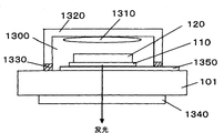
100 带电极透光性基板(有机LED元件用层叠体)100 Translucent substrate with electrodes (laminated body for organic LED elements)
101 玻璃基板101 glass substrate
102 散射层102 scattering layer
103 透光性电极103 Light-transmitting electrodes
104 散射物质104 Scattering matter
110 有机层110 organic layer
120 反射性电极120 reflective electrodes
具体实施方式 Detailed ways
(第一实施方式)(first embodiment)
以下,使用附图对本发明的带电极透光性基板(有机LED元件用层叠体)及具备有机LED元件用层叠体的有机LED元件进行说明。图1是表示有机LED元件用层叠体及具备有机LED元件用层叠体的有机LED元件的结构的剖视图。Hereinafter, the electrode-equipped translucent substrate (laminated body for an organic LED element) and the organic LED element including the laminated body for an organic LED element of the present invention will be described with reference to the drawings. FIG. 1 is a cross-sectional view showing the structure of a laminate for an organic LED element and an organic LED element including the laminate for an organic LED element.
本发明的有机LED元件,如图1所示,由带电极透光性基板(有机LED元件用层叠体)100、有机层110和反射性电极120构成。带电极透光性基板100由包含透光性玻璃基板的基板101、散射层102和透光性电极103构成。The organic LED element of the present invention is composed of a light-transmitting substrate with electrodes (a laminate for organic LED elements) 100 , an
本发明中使用的带电极透光性基板100,具备透光性玻璃基板101、在所述玻璃基板上形成的包含玻璃的散射层102和透光性电极103,所述散射层具备对于透射光的一个波长具有第一折射率的基材、和分散在所述基材中并且具有与所述基材不同的第二折射率的许多散射物质104,所述散射物质在所述散射层内的分布具有面内均匀性,并且在散射层的透光性电极面侧的表面附近,从所述散射层内部向所述透光性电极减少。而且,该透光性电极103具有高于所述第一折射率的第三折射率。The electrode-equipped
在此,散射层的透光性电极面侧的表面附近,是指从散射层的一半厚度处开始更靠近表面的一侧。Here, the surface vicinity of the light-transmitting electrode side of the scattering layer refers to the side closer to the surface from half the thickness of the scattering layer.
另外,面内均匀性并非通过形成图案来分布散射物质,而是指在整个面内分布。In addition, the in-plane uniformity does not mean that the scattering material is distributed by forming a pattern, but is distributed in the entire plane.
另外,包含玻璃的所述散射层102的一半厚度(δ/2)处的散射物质的密度ρ1与离所述散射层的、与所述透光性电极相对的一侧的表面(即基板侧的表面)的距离为x(δ/2<x≤δ处的散射物质的密度ρ2满足ρ1≥ρ2。In addition, the density ρ1 of the scattering material at half the thickness (δ/2) of the
另外,从另一种观点来看,离包含玻璃的所述散射层的透光性电极侧表面的距离为x(x≤0.2μm)处的散射物质的密度ρ3相对于距离x=2μm处的所述散射物质的密度ρ4满足ρ4>ρ3。关于这一点如后所述,从图26中也可以看出。另外,图27表示的是焙烧温度570℃和580℃的情况,但是,即使焙烧温度稍有变化也可以得到同样的结果。In addition, from another point of view, the density ρ of the scattering material at a distance x (x≤0.2 μm) from the light-transmitting electrode-side surface of the scattering layer containing glass is relative to that at a distance x=2 μm. The density ρ 4 of the scattering material satisfies ρ 4 >ρ 3 . This point will be described later, and it can also be seen from FIG. 26 . In addition, Fig. 27 shows the case where the firing temperature is 570°C and 580°C, but the same result can be obtained even if the firing temperature is slightly changed.
另外,再从另一观点来看,离包含玻璃的所述散射层的透光性电极一侧表面的距离为x(x≤0.2μm)处的散射物质的密度ρ3相对于距离x=5μm处的所述散射物质的密度ρ5满足ρ3>ρ5。关于这一点如后所述,从图27中也可以看出。In addition, from another point of view, the density ρ of the scattering material at the distance x (x≤0.2 μm) from the surface of the light-transmitting electrode side of the scattering layer including glass is relative to the distance x=5 μm The density ρ 5 of the scattering material at satisfies ρ 3 >ρ 5 . This point will be described later, and it can also be seen from FIG. 27 .
通过该构成,气泡、析出结晶或者包含与基材组成不同的材料的散射物质在包含玻璃层的散射层表层及紧靠表层的下方存在的概率比在散射层内部低,可以得到平滑的表面。因此,例如,形成有机EL元件时,透光性基板的表面即散射层表面平滑,因此在该上层上形成的透光性电极(第一电极)的表面平滑,在通过涂布法等在该上层上形成具有发光功能的层等时,也可以均匀地形成具有发光功能的层,透光性电极与在具有发光功能的层上形成的反射性电极(第二电极)表面间的电极间距离也均匀。结果,不会在具有发光功能的层上局部地施加大的电压,因此,可以实现长寿命化。另外,形成象高分辨率显示器这样由微小像素构成的显示装置时,需要形成微细的像素图案,虽然表面的凹凸不仅是像素的位置或尺寸产生偏差的原因,而且存在由于该凹凸而使有机EL元件短路的问题,但是,可以高精度地形成微细的图案。With this configuration, air bubbles, precipitated crystals, or scattering substances composed of a material different from that of the base material are less likely to exist in the surface layer of the scattering layer including the glass layer and immediately below the surface layer than in the inside of the scattering layer, and a smooth surface can be obtained. Therefore, for example, when an organic EL element is formed, the surface of the light-transmitting substrate, that is, the surface of the scattering layer is smooth, so the surface of the light-transmitting electrode (first electrode) formed on the upper layer is smooth, and the surface of the light-transmitting electrode (first electrode) formed on the upper layer is smooth. When a layer having a light-emitting function is formed on the upper layer, the layer having a light-emitting function can also be uniformly formed, and the distance between the electrodes between the light-transmitting electrode and the surface of the reflective electrode (second electrode) formed on the layer having a light-emitting function Also even. As a result, a large voltage is not locally applied to the layer having a light-emitting function, so that a longer lifetime can be achieved. In addition, when forming a display device composed of tiny pixels such as a high-resolution display, it is necessary to form a fine pixel pattern. Although the unevenness of the surface is not only the cause of the deviation of the position or size of the pixel, but also the organic EL due to the unevenness. The problem of component short circuit, however, can form fine patterns with high precision.
另外,散射层在玻璃基板上直接形成,但是,也可以在玻璃基板上通过溅射法形成二氧化硅薄膜后,隔着阻挡层形成散射层。但是,通过在玻璃基板上不隔着胶粘剂或有机层而形成包含玻璃的散射层,可以得到极稳定且平坦的表面,并且由于仅由无机物质构成,因此可以形成热稳定且长寿命的光器件。In addition, although the scattering layer is directly formed on the glass substrate, it is also possible to form the scattering layer through a barrier layer after forming a silicon dioxide thin film on the glass substrate by a sputtering method. However, by forming a scattering layer made of glass on a glass substrate without intervening an adhesive or an organic layer, an extremely stable and flat surface can be obtained, and since it is composed of only inorganic substances, a thermally stable and long-life optical device can be formed .
对于这样的透光性基板所具有的特性进行详细说明。The characteristics of such a translucent substrate will be described in detail.
焙烧玻璃粉末时,通过适当的方法涂布玻璃粉末的状态的示意图如图2所示。在此,表示的是构成本发明的透光性基板的散射层即玻璃层的最上部的剖面。像这样的散射物质在整个面上均匀分布的分布状态,例如可以通过使玻璃粒子G分散到溶剂或树脂与溶剂的混合物中并涂布到所需要的厚度来得到。例如,可以使用以最大长度计大小为约0.1μm~约10μm的玻璃粒子G。将树脂和溶剂混合时,通过对分散有玻璃粒子G的树脂膜进行加热,使树脂分解,可以得到图2的状态。图2是简略的图示,在玻璃粒子之间存在间隙。Fig. 2 shows a schematic diagram of a state where glass powder is coated by an appropriate method when firing glass powder. Here, the cross section of the uppermost part of the glass layer which is the scattering layer constituting the translucent substrate of the present invention is shown. Such a distribution state in which the scattering substance is uniformly distributed over the entire surface can be obtained, for example, by dispersing the glass particles G in a solvent or a mixture of a resin and a solvent and applying it to a desired thickness. For example, glass particles G having a size of about 0.1 μm to about 10 μm in maximum length can be used. When mixing the resin and the solvent, the resin film in which the glass particles G are dispersed is heated to decompose the resin, and the state shown in FIG. 2 can be obtained. Fig. 2 is a schematic diagram showing gaps between glass particles.
假设玻璃粒子G的玻璃粒子的大小存在分布,则推测会形成小玻璃粒子进入大玻璃粒子G间的间隙中的结构。另外,如果升高温度,则在比玻璃的软化温度低10~20℃的温度下,玻璃粒子开始相互熔合。此时的状态如图3所示。玻璃粒子如果相互熔合,则图2的玻璃粒子间形成的间隙由于玻璃的软化而变形,在玻璃中形成封闭的空间。在玻璃粒子的最上层,通过玻璃粒子的相互熔合而形成散射层102(玻璃层)的最表面。在最表面200上,未形成封闭空间的间隙以凹陷的形式存在。Assuming that there is a distribution in the size of the glass particles of the glass particles G, it is presumed that a structure in which small glass particles enter the gaps between the large glass particles G is formed. In addition, when the temperature is raised, glass particles start to fuse with each other at a
如果温度进一步上升,则玻璃的软化、流动继续进展,玻璃内部的间隙形成球形的气泡。在玻璃最表面200上,由玻璃粒子G的间隙造成的凹陷变平滑。该状态如图4所示。不仅玻璃粒子G的间隙形成气泡,而且有时玻璃软化时也会产生气体而形成气泡。例如,在玻璃层表面附着有机物时,有时该有机物分解产生CO2从而产生气泡。另外,也可以导入像这样受热分解的物质而主动地产生气泡。这样的状态通常可以在软化温度附近得到。玻璃的粘度在软化温度下高达107.6泊,气泡的大小如果为几微米以下,则不能上浮。因此,可以通过调节材料组成以产生小的气泡、并且进一步升高温度或者延长保持时间来抑制气泡的上浮,同时使表面更平滑。这样,如果从表面变平滑的状态开始冷却,则如图5所示,散射物质的密度具有面内均匀性、在表面比玻璃层内部小,可以得到表面平滑的玻璃散射层。If the temperature rises further, the softening and flow of the glass will continue to progress, and spherical bubbles will be formed in the gaps inside the glass. On the glass
这样,通过调节用于形成玻璃层的材料组成和焙烧温度,可以使气泡残留在玻璃层中,并且可以抑制在玻璃层最表面产生气泡或凹陷。即,可以调节焙烧温度分布并且调节焙烧时间,以防止散射物质的上升,使其残留于玻璃层中而不上升到表面,由此,可以提供散射特性优良、表面平滑性高的带电极透光性基板。In this way, by adjusting the composition of the material used to form the glass layer and the firing temperature, air bubbles can remain in the glass layer, and generation of air bubbles or depressions on the outermost surface of the glass layer can be suppressed. That is, it is possible to adjust the firing temperature distribution and adjust the firing time to prevent the scattering substances from rising, so that they remain in the glass layer and do not rise to the surface, thereby providing a light-transmitting charged electrode with excellent scattering characteristics and high surface smoothness. Sexual substrate.
另外,此时,根据处理温度、玻璃层用玻璃材料、玻璃粒子的大小和基板材料,玻璃层最表面有时存在波状起伏。其示意图如图6所示。在此,波状起伏是指周期λ为10μm以上的波状起伏。波状起伏的大小以波状起伏的粗糙度Ra计为约0.01μm至约5μm。即使存在这样的波状起伏时,也可以保持微细平滑性,即微观表面粗糙度Ra保持在30nm以下。In addition, at this time, depending on the processing temperature, the glass material for the glass layer, the size of the glass particles, and the substrate material, there may be undulations on the outermost surface of the glass layer. Its schematic diagram is shown in Figure 6. Here, waviness refers to waviness with a period λ of 10 μm or more. The magnitude of the waviness is about 0.01 μm to about 5 μm in terms of roughness Ra of the waviness. Even in the presence of such waviness, fine smoothness can be maintained, that is, the microscopic surface roughness Ra is maintained at 30 nm or less.
在此,波状起伏的粗糙度Ra和平均波长Rλa是指将短波长截止值设定为25.0μm、将长波长截止值设定为2.5mm,基于JIS B0601(2001年)标准(ISO97的翻译标准)计算的值。Here, the waviness roughness Ra and average wavelength Rλa mean that the short wavelength cutoff value is set to 25.0 μm and the long wavelength cutoff value is set to 2.5 mm, based on JIS B0601 (2001) standard (translation standard of ISO97) ) calculated value.
另外,表面粗糙度Ra是指微观(显微)观察的表面粗糙度,是指将长波长截止值设定为10μm,根据JIS B0601(1994年)计算的值。In addition, the surface roughness Ra refers to the surface roughness observed microscopically (microscopically), and is a value calculated based on JIS B0601 (1994) with the long-wavelength cutoff value set to 10 μm.
处理温度低的情况下,有时最表面有微小凹部残留,但是,通过延长焙烧时间,凹部的形状不会成为图7所示的悬垂形状,而是如图8所示变得平缓。在此,所谓悬垂,是指如图7所示,散射层表面与凹部的开口部附近处的切线所成的角度θ成为锐角,所谓平缓,是指图8中的θ为钝角或直角。凹部象这样平缓时,可以说由该凹部引起有机LED元件发生电极间短路的可能性较低。焙烧温度优选比玻璃化转变温度高约40℃至约60℃。温度如果过低,则焙烧不充分表面不平滑,因此更优选焙烧温度比玻璃化转变温度高约50℃至约60℃。When the treatment temperature is low, microscopic recesses may remain on the outermost surface. However, by prolonging the firing time, the shape of the recesses does not become the overhanging shape shown in FIG. 7 but becomes gentle as shown in FIG. 8 . Here, "overhanging" means that the angle θ formed by the tangent between the surface of the scattering layer and the vicinity of the opening of the recess is an acute angle as shown in FIG. When the concave portion is as flat as this, it can be said that the probability of short circuit between the electrodes of the organic LED element due to the concave portion is low. The firing temperature is preferably about 40°C to about 60°C higher than the glass transition temperature. If the temperature is too low, the firing will be insufficient and the surface will not be smooth, so the firing temperature is more preferably about 50°C to 60°C higher than the glass transition temperature.
另外,通过使用容易结晶的玻璃,可以使结晶在玻璃层内部析出。此时,结晶的大小如果为0.1μm以上,则作为光散射物质起作用。此时的状态如图9所示。通过适当地选择焙烧温度,可以抑制像这样的在玻璃层最表面的结晶析出,并且使结晶在玻璃层内部析出。具体而言,优选使温度升高到比玻璃化转变温度高约60℃至约100℃。如果以该程度升高温度,则玻璃的粘性高,气泡不会上浮。In addition, by using glass that is easy to crystallize, crystals can be precipitated inside the glass layer. At this time, if the size of the crystal is 0.1 μm or more, it functions as a light-scattering substance. The state at this time is shown in FIG. 9 . By appropriately selecting the firing temperature, such precipitation of crystals on the outermost surface of the glass layer can be suppressed and crystals can be precipitated inside the glass layer. Specifically, it is preferable to raise the temperature to about 60°C to about 100°C higher than the glass transition temperature. If the temperature is raised to this extent, the viscosity of the glass will be high, and air bubbles will not float up.
温度过高的情况下,在玻璃层最表面也析出结晶,最表面的平滑性丧失,因此不优选。示意图如图10所示。因此,更优选焙烧温度比玻璃化转变温度高约60℃至约80℃,最优选高约60℃至约70℃。通过这样的方法,可以使气泡或析出的结晶作为散射物质存在于玻璃层中,并且可以抑制它们在玻璃最表面产生。这些能够实现是因为玻璃在某一温度范围内自身平坦化,并且可以实现使气泡不上浮的高粘性,或者可以析出结晶。对于树脂而言,在上述高粘性下控制工艺是困难的,另外也不能析出结晶。When the temperature is too high, crystals are precipitated on the outermost surface of the glass layer, and the smoothness of the outermost surface is lost, which is not preferable. The schematic diagram is shown in Figure 10. Thus, the firing temperature is more preferably about 60°C to about 80°C above the glass transition temperature, most preferably about 60°C to about 70°C above. By such a method, air bubbles or precipitated crystals can be made to exist in the glass layer as scattering substances, and their generation on the outermost surface of the glass can be suppressed. These can be achieved because glass itself is flattened within a certain temperature range, and high viscosity that prevents air bubbles from floating can be realized, or crystals can be precipitated. For the resin, it is difficult to control the process under the above-mentioned high viscosity, and crystallization cannot be precipitated.
因此,通过调节材料组成或焙烧条件,可以得到所述散射层最表面的散射物质的密度小于所述散射层内部的散射物质的密度的透光性基板。Therefore, by adjusting the material composition or firing conditions, a light-transmitting substrate in which the density of the scattering substances on the outermost surface of the scattering layer is smaller than that of the scattering substances inside the scattering layer can be obtained.
另外,通过使用存在下述δ的透光性基板,可以得到具有充分的散射特性并且具有平滑表面的透光性基板,所述δ使包含玻璃的所述散射层的一半厚度处的散射物质的密度ρ1与离散射层最表面的距离x满足δ/2≤x≤δ的x处的散射物质的密度ρ2满足ρ1≥ρ2。In addition, a light-transmitting substrate having sufficient scattering properties and having a smooth surface can be obtained by using a light-transmitting substrate having a δ such that the scattering material at half the thickness of the scattering layer including glass Density ρ 1 and the distance x from the outermost surface of the scattering layer satisfy δ/2≤x≤δ, and the density ρ 2 of the scattering material at x satisfies ρ 1 ≥ ρ 2 .
另外,通过使散射层的表面形成构成弯曲面的波状起伏,可以在上层形成的有机EL元件为反射性电极时抑制映照造成的美观下降。使用反射性电极时,存在不发光时反射性电极产生映照而损害美观的问题,但是,根据本发明,在形成散射层时,通过优化条件,可以不使上层形成的图案的精度下降、或者不使电极间距离产生偏差,并且可以增大电极与具有发光功能的层的接触面积,因此可以增大有效元件面积,可以形成长寿命且高亮度的有机EL元件。In addition, by forming undulations constituting a curved surface on the surface of the scattering layer, it is possible to suppress deterioration of appearance due to reflection when the organic EL element formed on the upper layer is a reflective electrode. When a reflective electrode is used, there is a problem that the reflective electrode is reflected when it is not emitting light, and the appearance is impaired. However, according to the present invention, by optimizing the conditions when forming the scattering layer, it is possible not to reduce the precision of the pattern formed on the upper layer, or not The distance between the electrodes can be varied, and the contact area between the electrodes and the layer having a light-emitting function can be increased, so that the effective element area can be increased, and a long-life and high-brightness organic EL element can be formed.
另外,如图6中示意所示的波状起伏那样,优选该散射层表面的波状起伏的粗糙度Ra对表面波状起伏的波长Rλa的比Ra/Rλa为1.0×10-3以上、3.0×10-2以下。In addition, as in the waviness schematically shown in FIG. 6 , it is preferable that the ratio Ra/Rλa of the roughness Ra of the waviness on the surface of the scattering layer to the wavelength Rλa of the surface waviness is 1.0×10 −3 or more and 3.0×10 −3 or more. 2 or less.
另外,优选所述散射层表面的表面粗糙度Ra为30nm以下。更优选所述散射层的表面粗糙度为10nm以下。In addition, it is preferable that the surface roughness Ra of the surface of the scattering layer is 30 nm or less. More preferably, the surface roughness of the scattering layer is 10 nm or less.
例如,在这样的透光性基板上形成有机EL元件时,例如,透光性电极需要形成得较薄,该透光性电极可以不受基材的影响而形成的表面粗糙度为30nm以下,优选10nm以下。表面粗糙度如果超过30nm,则有时在其上形成的有机层的覆盖性变差,在玻璃散射层上形成的透光性电极与另一个电极之间有时发生短路。由于电极间短路导致元件不亮,但是,通过施加过电流,有时可以修复。从可以修复的角度考虑,玻璃散射层的表面粗糙度优选为10nm以下,更优选3nm以下。For example, when forming an organic EL element on such a light-transmitting substrate, for example, the light-transmitting electrode needs to be formed thinner, and the surface roughness that the light-transmitting electrode can be formed without being affected by the base material is 30 nm or less, It is preferably 10 nm or less. If the surface roughness exceeds 30 nm, the coverage of the organic layer formed thereon may deteriorate, and a short circuit may occur between the translucent electrode formed on the glass scattering layer and another electrode. The element does not light up due to a short circuit between electrodes, but it can sometimes be repaired by applying an overcurrent. From the viewpoint of repairability, the surface roughness of the glass scattering layer is preferably 10 nm or less, more preferably 3 nm or less.
另外,已知某些材料系在焙烧温度为570℃以上时可以使表面粗糙度Ra为10nm以下。最佳焙烧条件因材料系而不同,通过控制散射物质的种类和大小,可以抑制散射物质在最表面的存在,从而得到表面平滑性优良的散射层。In addition, it is known that some material systems can have a surface roughness Ra of 10 nm or less when the firing temperature is 570° C. or higher. Optimum firing conditions vary with material systems. By controlling the type and size of scattering substances, the existence of scattering substances on the outermost surface can be suppressed, thereby obtaining a scattering layer with excellent surface smoothness.
另外,就散射物质的大小而言,当散射层中存在气泡时,如果气泡变大则在焙烧等散射层形成工艺中浮力变大,容易上浮,到达最表面时气泡破裂,有可能使表面平滑性显著下降。另外,该部分的散射物质的数量相对减少,因此仅该部分的散射性下降。如果象这样聚集大的气泡,则成为斑点而可被观察到。另外,直径5μm以上的气泡的比例优选为15体积%以下,更优选10%以下,进一步优选7体积%以下。另外,散射物质为气泡以外的物质时,由于该部分的散射物质的数量相对减少,因此仅该部分的散射性变差。因此,最大长度为5μm以上的散射物质的比例优选为15体积%以下,更优选10体积%以下,进一步优选7体积%以下。In addition, in terms of the size of the scattering material, when there are bubbles in the scattering layer, if the bubbles become larger, the buoyancy will increase during the formation process of the scattering layer such as firing, and they will easily float up. Sex decreased significantly. In addition, since the number of scattering substances in this portion is relatively reduced, only the scattering property of this portion is reduced. If large air bubbles gather in this way, they will be observed as spots. In addition, the proportion of bubbles having a diameter of 5 μm or more is preferably 15% by volume or less, more preferably 10% by volume or less, and still more preferably 7% by volume or less. In addition, when the scattering material is a material other than air bubbles, since the number of scattering materials in this part is relatively small, the scattering property of only this part is deteriorated. Therefore, the proportion of scattering substances having a maximum length of 5 μm or more is preferably 15 vol % or less, more preferably 10 vol % or less, and further preferably 7 vol % or less.
另外,使用反射性电极时,存在不发光时反射性电极产生映照,从而损害美观的问题,但是,在形成散射层时通过优化条件,可以在散射层表面形成波状起伏形状。对形成的散射层表面的波状起伏进行测定。测定使用东京精密制SURFCOM1400D。在此,截止波长设定为2.5mm。然后,在该带散射层的玻璃基板上真空蒸镀80nm的铝,并测定铝层的成膜面的扩散反射率,计算散射光的比例。测定使用PERKINELMER公司制造的LANBDA 950。In addition, when a reflective electrode is used, there is a problem that the reflective electrode is reflected when not emitting light, thereby impairing the appearance. However, by optimizing the conditions when forming the scattering layer, it is possible to form a wave-like undulation on the surface of the scattering layer. The waviness of the surface of the formed scattering layer was measured. For the measurement, SURFCOM1400D manufactured by Tokyo Seiki was used. Here, the cutoff wavelength was set to 2.5 mm. Then, 80 nm of aluminum was vacuum-deposited on the glass substrate with the scattering layer, and the diffuse reflectance of the film-forming surface of the aluminum layer was measured to calculate the ratio of scattered light. For the measurement, LANBDA 950 manufactured by PERKINELMER was used.
结果如表1所示。The results are shown in Table 1.
表1Table 1

在此,A是将P2O5为23.1摩尔%、B2O3为12.0摩尔%、Li2O为11.6摩尔%、Bi2O3为16.6摩尔%、TiO2为8.7摩尔%、Nb2O5为17.6摩尔%、WO3为10.4摩尔%的材料在各温度下焙烧而得到的材料;B是将Bi2O3减至5.5摩尔%、并且追加4摩尔%Na2O和2.5摩尔%K2O的材料在530℃焙烧而得到的材料;C是散射层由表12所示组成的材料构成并进行焙烧而得到的材料。A的玻璃化转变温度Tg为499℃,B为481℃。Here, A is 23.1 mol% of P 2 O 5 , 12.0 mol % of B 2 O 3 , 11.6 mol % of Li 2 O , 16.6 mol % of Bi 2 O 3 , 8.7 mol % of TiO 2 , and Nb 2 O 5 is 17.6 mol%, WO 3 is 10.4 mol% of the material obtained by firing at various temperatures; B is a material obtained by reducing Bi 2 O 3 to 5.5 mol%, and adding 4 mol% Na 2 O and 2.5 mol% The material of K 2 O was calcined at 530° C.; C was a material in which the scattering layer was composed of the materials shown in Table 12 and calcined. The glass transition temperature Tg of A is 499°C, and that of B is 481°C.
通过这样调节焙烧条件,可以使表面具有波状起伏,由此可以减弱镜面反射性。因此,即使在散射层的散射性小的情况下,也可以减少由于反射电极具有镜面性而造成的映照。在此,前面已经提到优选波状起伏的粗糙度Ra与所述表面的波状起伏的波长Rλa的比(Ra/Rλa)为1.0×10-3以上、3.0×10-2以下,这一点从表1也可以得到确认。表1中C的Ra小而使该比(Ra/Rλa)小于1.0×10-3,因此不能得到充分的扩散反射比。另外,Rλa大或者波状起伏的粗糙度Ra小而使该比(Ra/Rλa)小于1.0×10-3时,不能得到充分的扩散反射比。另外,波状起伏的粗糙度大而使该比(Ra/Rλa)超过3.0×10-2时,难以形成器件。By adjusting the firing conditions in this way, the surface can be given undulations, thereby reducing specular reflectivity. Therefore, even when the scattering properties of the scattering layer are small, reflections due to the specularity of the reflective electrode can be reduced. Here, it has been mentioned above that the ratio (Ra/Rλa) of the roughness Ra of the waviness to the wavelength Rλa of the waviness of the surface is preferably 1.0×10 −3 or more and 3.0×10 −2 or less. 1 can also be confirmed. Ra of C in Table 1 is so small that the ratio (Ra/Rλa) is less than 1.0×10 -3 , so sufficient diffuse reflectance cannot be obtained. Also, when Rλa is large or the roughness Ra of the waviness is small so that the ratio (Ra/Rλa) is less than 1.0×10 -3 , sufficient diffuse reflectance cannot be obtained. In addition, when the roughness of the waviness is so large that the ratio (Ra/Rλa) exceeds 3.0×10 -2 , it is difficult to form a device.
另外,所述散射层中的所述散射物质的含量优选为至少1体积%。In addition, the content of the scattering substance in the scattering layer is preferably at least 1% by volume.
从实验结果可知,当含有1体积%以上的散射物质时,能够得到充分的光散射性。更优选含有5体积%以上散射物质时,可以得到更良好的光散射性。From the experimental results, it can be seen that sufficient light-scattering properties can be obtained when the scattering substance is contained in an amount of 1 volume % or more. More preferably, when the scattering substance is contained in an amount of 5% by volume or more, better light scattering properties can be obtained.
另外,作为散射物质,存在下述情况:气泡、具有与基层不同组成的材料粒子及基层的析出结晶,这些情况可以单独存在,也可以混合存在。In addition, as scattering substances, there are bubbles, material particles having a composition different from that of the base layer, and precipitated crystals of the base layer, and these may exist alone or in combination.
散射物质为气泡时,通过调节焙烧温度等焙烧条件,可以调节气泡的大小、气泡分布或密度。When the scattering material is bubbles, the size, distribution or density of the bubbles can be adjusted by adjusting the firing conditions such as the firing temperature.
散射物质为具有与基层不同组成的材料粒子时,通过调节材料组合物、调节焙烧温度等焙烧条件,可以调节散射物质的大小、分布或密度。When the scattering material is a material particle having a composition different from that of the base layer, the size, distribution or density of the scattering material can be adjusted by adjusting the material composition, adjusting the firing temperature and other firing conditions.
所述散射物质为构成所述基层的玻璃的析出结晶时,通过调节焙烧温度等焙烧条件,可以调节气泡的大小、气泡分布或密度。When the scattering material is a precipitated crystal of the glass constituting the base layer, the size, distribution or density of the bubbles can be adjusted by adjusting the firing conditions such as firing temperature.
在各种情况下本发明的散射层通过涂布和焙烧,均得到包含散射物质的玻璃层,因此基本上散射物质的面内分布大致均匀。Coating and firing of the scattering layer according to the invention in each case results in a glass layer comprising scattering substances, so that essentially the in-plane distribution of the scattering substances is approximately homogeneous.
另外,优选基层对于波长λ(430nm<λ<650nm)中的至少一个波长的第一折射率为1.8以上,但是形成高折射率材料层比较困难。因此,在本发明中,在使用基层的第一折射率比作为透光性电极的折射率的第三折射率小的物质时,通过调节玻璃材料中的散射物质,可以容易地进行折射率的调节、容易地提高提取效率。In addition, it is preferable that the first refractive index of the base layer for at least one of the wavelengths λ (430nm<λ<650nm) is 1.8 or higher, but it is difficult to form a high refractive index material layer. Therefore, in the present invention, when using a substance whose first refractive index of the base layer is smaller than the third refractive index as the refractive index of the light-transmitting electrode, by adjusting the scattering substance in the glass material, the refractive index can be easily adjusted. Adjustable, easy to improve extraction efficiency.
另外,在此,对于面内均匀性进行了说明,虽然优选散射物质在面内的分布均匀,但是也可以不均匀。In addition, here, the in-plane uniformity has been described, and although the in-plane distribution of the scattering material is preferably uniform, it may not be uniform.
另外,对于散射物质在深度方向的分布而言,也不限于所述实施方式,可以适当变更。In addition, the distribution of the scattering material in the depth direction is not limited to the above-described embodiment, and can be appropriately changed.
以下对各构件进行详细说明。Each member will be described in detail below.
<基板><substrate>
作为透光性基板的形成中使用的透光性基板101,主要可以使用玻璃基板等对可见光的透射率高的材料。透射率高的材料,具体而言,除了玻璃基板以外还可以使用塑料基板。作为玻璃基板的材料,有碱性玻璃、无碱玻璃或石英玻璃等无机玻璃。另外,作为塑料基板的材料,有聚酯、聚碳酸酯、聚醚、聚砜、聚醚砜、聚乙烯醇以及聚偏二氟乙烯和聚氟乙烯等含氟聚合物。另外,为了防止水分透过基板,塑料基板也可以采用具有阻挡性的构成。透光性基板101的厚度在玻璃的情况下优选为0.1mm~2.0mm。但是,过薄会导致强度下降,因此特别优选为0.5mm~1.0mm。As the light-transmitting
另外,用玻璃粉制作散射层时,会产生应变等问题,因此优选热膨胀系数为50×10-7/℃以上、优选70×10-7/℃以上、更优选80×10-7/℃以上。In addition, when the scattering layer is made of glass frit, there will be problems such as strain, so the thermal expansion coefficient is preferably 50×10 -7 /°C or higher, preferably 70×10 -7 /°C or higher, more preferably 80×10 -7 /°C or higher .
另外,优选散射层在100℃至400℃下的平均热膨胀系数为70×10-7/℃至95×10-7/℃,并且玻璃化转变温度为450℃至550℃。In addition, it is preferable that the scattering layer has an average coefficient of thermal expansion at 100°C to 400°C of 70×10 -7 /°C to 95×10 -7 /°C, and a glass transition temperature of 450°C to 550°C.
<散射层><scattering layer>
以下,对散射层的构成、制作方法、特性及折射率的测定方法进行详细说明。另外,细节如后所述,为了实现本发明的主旨即提高光提取效率,散射层的折射率必须与透光性电极材料的折射率同等或者更高。本发明中,尽管构成散射层的基层所具有的第一折射率小,但是通过调节散射物质可以实现折射率与作为透光性电极材料的折射率的第三折射率同等或更高的散射层。Hereinafter, the configuration, production method, characteristics, and measurement method of the refractive index of the scattering layer will be described in detail. In addition, as will be described later in detail, in order to realize the gist of the present invention, that is, to improve the light extraction efficiency, the refractive index of the scattering layer must be equal to or higher than that of the light-transmitting electrode material. In the present invention, although the first refractive index of the base layer constituting the scattering layer is small, the scattering layer having a refractive index equal to or higher than the third refractive index of the light-transmitting electrode material can be realized by adjusting the scattering material. .
(计算方法)(calculation method)
本发明人为了得到后述的散射层特性,进行了光学模拟,对于各个参数,分别考查了其对提取效率的影响。使用的计算软件为OPTIS公司制作的软件SPEOS。本软件为光线跟踪软件,同时散射层可以应用Mie散射的理论公式。实际上作为具有电荷注入/输送层、发光层等发光功能的层使用的有机层的厚度实际合计为约0.1μm~约0.3μm,但是由于在光线跟踪中,即使厚度变化光线的角度也不变化,因此,软件允许的最小厚度设定为1μm。玻璃基板和散射层的合计厚度由于同样的原因也设定为100μm。另外,为了简单起见,将有机层及透光性电极分为电子注入层及发光层、空穴注入/输送层和透光性电极三部分进行计算。计算中设定它们的折射率相同,由于有机层与透光性电极的折射率为相同程度的值,因而计算结果不会有大的变化。另外,由于有机层较薄,因此,虽然严格而言建立了干涉波导模式,但是,即使进行几何光学处理,结果也不会发生大的变化,因此,通过计算来估计本次发明的效果就足够了。有机层中,发射光无指向性地从总共六个面射出。设定总光通量为1000lm、光线根数为10万根或100万根进行计算。从透光性基板射出的光在设置于透光性基板的上方10μm处的受光面被捕捉,由其照度计算提取效率。The inventors of the present invention performed optical simulations in order to obtain the characteristics of the scattering layer described later, and examined the influence of each parameter on the extraction efficiency. The calculation software used is the software SPEOS produced by OPTIS. This software is a ray tracing software, and the theoretical formula of Mie scattering can be applied to the scattering layer. In fact, the thickness of the organic layer used as a layer having a light-emitting function such as a charge injection/transport layer and a light-emitting layer is actually about 0.1 μm to about 0.3 μm in total. However, in ray tracing, the angle of light does not change even if the thickness changes. , therefore, the minimum thickness allowed by the software was set to 1 μm. The total thickness of the glass substrate and the scattering layer was also set to 100 μm for the same reason. In addition, for the sake of simplicity, the organic layer and the light-transmitting electrode are divided into three parts, the electron injection layer and the light-emitting layer, the hole injection/transporting layer, and the light-transmitting electrode for calculation. In the calculation, these refractive indices are assumed to be the same, and since the refractive indices of the organic layer and the light-transmitting electrode have approximately the same value, there is no significant change in the calculation result. Also, since the organic layer is thin, although the interference waveguide mode is strictly speaking established, the result does not change greatly even if geometrical optics processing is performed, so it is sufficient to estimate the effect of this invention by calculation up. In the organic layer, emitted light is emitted from a total of six surfaces in a non-directional manner. Set the total luminous flux as 1000lm and the number of rays as 100,000 or 1 million for calculation. The light emitted from the light-transmitting substrate was captured by the light-receiving surface provided at 10 μm above the light-transmitting substrate, and the extraction efficiency was calculated from the illuminance thereof.
(构成)(constitute)
本实施方式中,散射层102如前所述是通过利用涂布等方法在玻璃基板上形成玻璃粉末,并在所需的温度下焙烧而形成的,其包含具有第一折射率的基材102和分散在所述基材102中的、具有与所述基材不同的第二折射率的许多散射物质104,并且,所述散射物质在所述散射层中的层内分布从所述散射层内部向最表面减少,通过使用玻璃层,如前所述,可以在具有优良的散射特性的同时保持表面的平滑性,并且通过在发光器件等的光射出面侧使用,可以实现极高效率的光提取。In this embodiment, as mentioned above, the
另外,作为散射层,使用具有带涂层的主表面的、光透射率高的材料(基材)。作为基材,使用玻璃、结晶玻璃、透光树脂、透光陶瓷。作为玻璃的材料,有钠钙玻璃、硼硅玻璃、无碱玻璃、石英玻璃等无机玻璃。另外,在基材的内部,形成有许多散射物质104(例如有:气泡、析出结晶、与基材不同的材料粒子、分相玻璃)。在此,粒子是指小的固体物质,例如有填料或陶瓷。另外,气泡是指空气或气体的物体。另外,分相玻璃是指由两种以上的玻璃相构成的玻璃。另外,散射物质为气泡时,散射物质的直径是指空隙的长度。In addition, as the scattering layer, a material (substrate) having a coated main surface and having a high light transmittance is used. As the substrate, glass, crystallized glass, light-transmitting resin, and light-transmitting ceramics are used. Examples of glass materials include inorganic glasses such as soda lime glass, borosilicate glass, alkali-free glass, and quartz glass. In addition, inside the substrate, many scattering substances 104 (for example, air bubbles, precipitated crystals, material particles different from the substrate, and phase-separated glass) are formed. Particles here mean small solid substances, for example filled or ceramic. In addition, a bubble refers to an object of air or gas. In addition, phase-separated glass refers to glass composed of two or more glass phases. In addition, when the scattering material is a bubble, the diameter of the scattering material refers to the length of the void.
另外,为了实现本发明本来的主要目的即光提取效率的提高,基材的折射率必须与透光性电极材料的折射率同等或者更高。这是因为折射率低时,在基材与透光性电极材料的界面处产生全反射损耗。因此,本发明中,即使基材的折射率小,也可以通过散射物质的分布来补偿提取效率,从而使散射层整体的折射率与透光性电极的折射率同等或更高,提高提取效率。在此,散射层的折射率只要至少在发光层的发射光谱范围的一部分(例如,红、蓝、绿等)中超过透光性电极材料的折射率即可,优选在发射光谱的全范围(430nm~650nm)中超过,更优选在可见光的全波长范围(360nm~830nm)中超过。In addition, in order to improve the light extraction efficiency which is the original main purpose of the present invention, the refractive index of the substrate must be equal to or higher than that of the light-transmitting electrode material. This is because total reflection loss occurs at the interface between the substrate and the light-transmitting electrode material when the refractive index is low. Therefore, in the present invention, even if the refractive index of the substrate is small, the extraction efficiency can be compensated by the distribution of scattering substances, so that the overall refractive index of the scattering layer is equal to or higher than that of the light-transmitting electrode, and the extraction efficiency can be improved. . Here, the refractive index of the scattering layer only needs to exceed the refractive index of the light-transmitting electrode material in at least a part of the emission spectrum range (for example, red, blue, green, etc.) of the light-emitting layer, preferably in the entire range of the emission spectrum ( 430nm to 650nm), more preferably in the entire wavelength range of visible light (360nm to 830nm).
另外,为了防止有机LED元件的电极间短路,散射层主表面必须平滑。因此,不优选散射物质从散射层的主表面突出。为了使散射物质不从散射层的主表面突出,优选散射物质不存在于离散射层的主表面0.2μm以内处。散射层的主表面的JIS B0601-1994规定的算术平均粗糙度(表面粗糙度:Ra)优选为30nm以下,更优选10nm以下(参考表1),特别优选为1nm以下。散射物质与基材的折射率无论哪一个高都可以,但是,优选折射率之差(Δn)至少在发光层的发射光谱范围的一部分中为0.2以上。为了得到充分的散射特性,更优选折射率之差(Δn)在发射光谱全范围(430nm~650nm)或可见光的全波长范围(360nm~830nm)中为0.2以上。In addition, in order to prevent short-circuiting between electrodes of the organic LED element, the main surface of the scattering layer must be smooth. Therefore, it is not preferable that the scattering substance protrudes from the main surface of the scattering layer. In order for the scattering substance not to protrude from the main surface of the scattering layer, it is preferable that the scattering substance does not exist within 0.2 μm from the main surface of the scattering layer. The arithmetic mean roughness (surface roughness: Ra) specified in JIS B0601-1994 of the main surface of the scattering layer is preferably 30 nm or less, more preferably 10 nm or less (see Table 1), particularly preferably 1 nm or less. The refractive index of the scattering material and the substrate may be higher, but it is preferable that the difference (Δn) in the refractive index is at least 0.2 in at least a part of the emission spectrum range of the light emitting layer. In order to obtain sufficient scattering properties, it is more preferable that the difference in refractive index (Δn) is 0.2 or more over the entire range of the emission spectrum (430nm to 650nm) or the entire wavelength range of visible light (360nm to 830nm).
为了得到最大的折射率差,优选上述高透光率材料由高折射率玻璃构成,散射物质由气体的物体即气泡构成。本发明中,基材的折射率可以小于透光性电极的折射率,因此,可以提高可使用的材料的选择自由度。但是,此时,也优选基材的折射率尽可能高,因此,优选使用高折射率的玻璃作为基材。作为高折射率玻璃的成分,可以使用含有选自P2O5、SiO2、B2O3、Ge2O、TeO2的一种或两种以上的成分作为网络形成剂,并且含有选自TiO2、Nb2O5、WO3、Bi2O3、La2O3、Gd2O3、Y2O3、ZrO2、ZnO、BaO、PbO、Sb2O3的一种或两种以上的成分作为高折射率成分的高折射率玻璃。此外,在调节玻璃特性的意义上考虑,可以在无损对折射率所要求的物性的范围内使用碱金属氧化物、碱土金属氧化物、氟化物等。作为具体的玻璃体系,可以列举B2O3-ZnO-La2O3系、P2O5-B2O3-R’2O-R”O-TiO2-Nb2O5-WO3-Bi2O3系、TeO2-ZnO系、B2O3-Bi2O3系、SiO2-Bi2O3系、SiO2-ZnO系、B2O3-ZnO系、P2O5-ZnO系等。在此,R’表示碱金属元素、R”表示碱土金属元素。另外,以上是例子,只要是满足上述条件的构成即可,不限于这些例子。In order to obtain the largest refractive index difference, it is preferable that the above-mentioned high light transmittance material is made of high refractive index glass, and the scattering material is made of gaseous objects, that is, air bubbles. In the present invention, the refractive index of the substrate can be lower than that of the light-transmitting electrode, and therefore, the degree of freedom of selection of usable materials can be increased. However, also in this case, it is preferable that the refractive index of the substrate is as high as possible, and therefore, it is preferable to use glass with a high refractive index as the substrate. As a component of high refractive index glass, one or two or more components selected from P2O5, SiO2, B2O3, Ge2O, and TeO2 can be used as network formers , and the components selected from One or two of TiO 2 , Nb 2 O 5 , WO 3 , Bi 2 O 3 , La 2 O 3 , Gd 2 O 3 , Y 2 O 3 , ZrO 2 , ZnO, BaO, PbO, Sb 2 O 3 The above-mentioned components are high-refractive-index glasses that are high-refractive-index components. In addition, in the sense of adjusting the properties of the glass, alkali metal oxides, alkaline earth metal oxides, fluorides, and the like can be used within a range that does not impair the physical properties required for the refractive index. Specific glass systems include B 2 O 3 -ZnO-La 2 O 3 systems, P 2 O 5 -B 2 O 3 -R' 2 OR"O-TiO 2 -Nb 2 O 5 -WO 3 -Bi 2 O 3 system, TeO 2 -ZnO system, B 2 O 3 -Bi 2 O 3 system, SiO 2 -Bi 2 O 3 system, SiO 2 -ZnO system, B 2 O 3 -ZnO system, P 2 O 5 - ZnO system, etc. Here, R' represents an alkali metal element, and R" represents an alkaline earth metal element. In addition, the above are examples, and it is not limited to these examples as long as the above-mentioned conditions are satisfied.
通过使基材具有特定的透射率光谱,还可以改变发光的色调。作为着色剂,可以单独或组合使用过渡金属氧化物、稀土金属氧化物、金属胶体等公知的着色剂。By giving the substrate a specific transmittance spectrum, it is also possible to change the hue of the emission. As the colorant, known colorants such as transition metal oxides, rare earth metal oxides, and metal colloids can be used alone or in combination.
在此,一般而言,在背光源或照明用途中,需要发白光。白色化的方法已知有:在空间上分别涂布红、蓝、绿的方法(分别涂布法)、将具有不同发光色的发光层层叠的方法(层叠法)、将蓝色光源发射的光通过空间上分离设置的色转换材料进行转换的方法(色转换法)。在背光源或照明用途中,只要得到均匀的白色即可,因此一般使用层叠法。层叠的发光层有使用通过加色混合而显白色的组合的情况,例如蓝绿层与橙色层层叠的情况或红、蓝、绿层叠的情况。特别是在照明用途中,照射面上的色再现性很重要,因此,优选具有可见光区域所需的发射光谱。将蓝绿层与橙色层层叠时,由于绿色的发光强度低,因此照亮含有大量绿色的物体时,色再现性变差。层叠方法具有不必在空间上改变色配置的优点,但另一方面具有以下两个问题。第一个问题是如上所述由于有机层的膜厚度薄,因此提取出的发射光受到干涉的影响。因此,色调随观察角度的不同而变化。白色的情况下,人眼对色调的敏感度高,因此,这样的现象成为问题。第二个问题是发光期间,载流子平衡偏移,因此各色的发光亮度变化,色调发生变化。Here, in general, white light emission is required for backlight or lighting applications. Whitening methods are known: a method of spatially coating red, blue, and green (separate coating method), a method of laminating light-emitting layers with different luminous colors (lamination method), and a method of emitting blue light sources. A method in which light is converted by means of spatially separated color conversion materials (color conversion method). In backlight or lighting applications, it is only necessary to obtain a uniform white color, so the lamination method is generally used. The laminated light-emitting layer may use a combination that expresses white by additive color mixing, for example, the case where a cyan layer and the orange layer are laminated, or the case where red, blue, and green are laminated. Especially in lighting applications, color reproducibility on the irradiated surface is important, and therefore, it is preferable to have an emission spectrum required in the visible light region. When the blue-green layer is laminated with the orange layer, since the luminous intensity of green is low, color reproducibility deteriorates when illuminating an object containing a large amount of green. The lamination method has the advantage of not having to change the color configuration spatially, but on the other hand has the following two problems. The first problem is that the extracted emitted light is affected by interference due to the thin film thickness of the organic layer as described above. Therefore, the hue changes with different viewing angles. In the case of white, since the sensitivity of the human eye to hue is high, such a phenomenon becomes a problem. The second problem is that the carrier balance shifts during light emission, so that the light emission brightness of each color changes and the color tone changes.
现有的有机LED元件,没有使荧光体分散到散射层或扩散层中的构思,因此,不能解决上述色调发生变化的问题。因此,现有的有机LED元件作为背光源或照明用途还不充分。但是,本发明的有机LED元件用基板及有机LED元件,可以使用荧光性物质作为散射物质或基材。因此,通过有机层的发光,可以实现进行波长转换、使色调变化的效果。此时,可以减少有机LED的发光色,并且由于发射光经散射后射出,因此,可以抑制色调的角度依赖性和色调的经时变化。Conventional organic LED elements do not have the concept of dispersing phosphors in the scattering layer or diffusion layer, and therefore cannot solve the above-mentioned problem of color tone change. Therefore, existing organic LED elements are not sufficient for backlight or lighting applications. However, the substrate for an organic LED element and the organic LED element of the present invention may use a fluorescent substance as a scattering substance or a base material. Therefore, by the light emission of the organic layer, the effect of performing wavelength conversion and changing color tone can be realized. In this case, the emission color of the organic LED can be reduced, and since the emitted light is scattered and emitted, the angular dependence of the hue and the temporal change of the hue can be suppressed.
(散射层的制作方法)(How to make the scattering layer)
散射层的制作方法通过涂布和焙烧来进行,特别是从在大面积上均匀且迅速地形成10~100μm的厚膜的观点考虑,优选将玻璃制成玻璃粉浆料后进行制作的方法。为了应用玻璃粉浆料法,并且为了抑制基板玻璃的热变形,优选散射层的玻璃的软化点(Ts)低于基板玻璃的应变点(SP),并且热膨胀系数α的差小。优选软化点与应变点的差为30℃以上,更优选50℃以上。另外,散射层与基板玻璃的膨胀率差优选为±10×10-7/K以下,更优选±5×10-7/K以下。在此,玻璃粉浆料是指将玻璃粉末分散到树脂、溶剂、填料等中而形成的浆料。使用丝网印刷等图案形成技术将玻璃粉浆料图案化并进行焙烧,由此可以覆盖玻璃层。以下说明技术概要。The scattering layer is produced by coating and firing. In particular, from the viewpoint of uniformly and rapidly forming a thick film of 10 to 100 μm over a large area, the method of forming the glass into a glass frit paste is preferable. In order to apply the glass frit paste method and to suppress thermal deformation of the substrate glass, it is preferable that the softening point (Ts) of the glass of the scattering layer is lower than the strain point (SP) of the substrate glass and that the difference in thermal expansion coefficient α is small. The difference between the softening point and the strain point is preferably 30°C or higher, more preferably 50°C or higher. In addition, the expansion coefficient difference between the scattering layer and the substrate glass is preferably ±10×10 -7 /K or less, more preferably ±5×10 -7 /K or less. Here, the glass frit paste refers to a paste formed by dispersing glass powder in a resin, a solvent, a filler, or the like. The glass frit paste is patterned and fired using a patterning technique such as screen printing, thereby covering the glass layer. The technical outline is described below.
(玻璃粉浆料材料)(glass frit paste material)
1.玻璃粉末1. Glass powder
玻璃粉末粒径为1μm~10μm。为了控制焙烧后的膜的热膨胀,有加入填料的方法。填料具体地可以使用二氧化锆、二氧化硅、氧化铝等,粒径为0.1μm~20μm。The particle size of the glass powder is 1 μm to 10 μm. In order to control the thermal expansion of the film after firing, there is a method of adding fillers. Specifically, zirconia, silica, alumina, etc. can be used as the filler, and the particle size is 0.1 μm to 20 μm.
以下对玻璃材料进行说明。The glass material will be described below.
本发明中,所述散射层使用如下材料:包含20~30摩尔%P2O5、3~14摩尔%B2O3、总量为10~20摩尔%的Li2O、Na2O和K2O、10~20摩尔%Bi2O3、3~15摩尔%TiO2、10~20摩尔%Nb2O5和5~15摩尔%WO3,以上成分的总量为90摩尔%以上。In the present invention, the scattering layer uses the following materials: 20-30 mole % of P 2 O 5 , 3-14 mole % of B 2 O 3 , 10-20 mole % of Li 2 O, Na 2 O and K 2 O, 10-20 mol% Bi 2 O 3 , 3-15 mol% TiO 2 , 10-20 mol% Nb 2 O 5 and 5-15 mol% WO 3 , the total amount of the above components being 90 mol% or more .
作为形成散射层的玻璃组成,只要可以得到所需的散射特性并且玻璃粉浆料化后可以焙烧,则没有特别限制,为了使提取效率最大化,可以列举例如:含有P2O5作为必须成分,并且还含有Nb2O5、Bi2O3、TiO2、WO3中的一种以上成分的体系;含有B2O3、ZnO和La2O3作为必须成分,并且还含有Nb2O5、ZrO2、Ta2O5、WO3中的一种以上成分的体系;含有SiO2作为必须成分,并且还含有Nb2O5、TiO2中的一种以上成分的体系;以及含有Bi2O3作为主成分,并且含有SiO2、B2O3等作为网络形成成分的体系等。The composition of the glass forming the scattering layer is not particularly limited as long as the desired scattering characteristics can be obtained and the glass frit can be fired after slurrying. In order to maximize the extraction efficiency, for example, P2O5 is included as an essential component . , and also contains more than one of Nb 2 O 5 , Bi 2 O 3 , TiO 2 , WO 3 system; contains B 2 O 3 , ZnO and La 2 O 3 as essential components, and also contains Nb 2 O 5. A system containing one or more components of ZrO 2 , Ta 2 O 5 , and WO 3 ; a system containing SiO 2 as an essential component, and also containing one or more components of Nb 2 O 5 , TiO 2 ; and a system containing Bi A system containing 2 O 3 as a main component and SiO 2 , B 2 O 3 , etc. as a network forming component, or the like.
另外,本发明中,在作为散射层使用的所有玻璃体系中,除了作为来自原料的杂质而不可避免地混入的情况以外,不含有作为对环境产生不利影响的成分的As2O3、PbO、CdO、ThO2、HgO。In addition, in the present invention, all the glass systems used as the scattering layer do not contain As 2 O 3 , PbO, CdO, ThO2 , HgO.
含有P2O5、并且含有Nb2O5、Bi2O3、TiO2、WO3中的一种以上成分的散射层,以摩尔%计,优选如下组成范围的玻璃:P2O5为15~30%、SiO2为0~15%、B2O3为0~18%、Nb2O5为5~40%、TiO2为0~15%、WO3为0~50%、Bi2O3为0~30%并且Nb2O5+TiO2+WO3+Bi2O3为20~60%、Li2O为0~20%、Na2O为0~20%、K2O为0~20%并且Li2O+Na2O+K2O为5~40%、MgO为0~10%、CaO为0~10%、SrO为0~10%、BaO为0~20%、ZnO为0~20%、Ta2O5为0~10%。The scattering layer containing P 2 O 5 and one or more of Nb 2 O 5 , Bi 2 O 3 , TiO 2 , and WO 3 is preferably a glass with the following composition range in mole percent: P 2 O 5 is 15-30%, SiO 2 0-15%, B 2 O 3 0-18%, Nb 2 O 5 5-40%, TiO 2 0-15%, WO 3 0-50%, Bi 2 O 3 is 0-30%, Nb 2 O 5 +TiO 2 +WO 3 +Bi 2 O 3 is 20-60%, Li 2 O is 0-20%, Na 2 O is 0-20%, K 2 O is 0-20% and Li2O + Na2O + K2O is 5-40%, MgO is 0-10%, CaO is 0-10%, SrO is 0-10%, and BaO is 0-20%. %, 0-20% for ZnO, and 0-10% for Ta 2 O 5 .
各成分的效果以摩尔%计如下所述。The effect of each component is as follows in mol%.
P2O5是形成该玻璃体系的骨架并使其玻璃化的必须成分,含量过小时,玻璃的失透性变大,不能得到玻璃,因此优选15%以上,更优选18%以上。另一方面,含量过大则折射率下降,因此不能实现发明的目的。因此,含量优选为30%以下,更优选28%以下。P 2 O 5 is an essential component for forming the skeleton of the glass system and vitrifying it. If the content is too small, the devitrification of the glass will increase and glass cannot be obtained. Therefore, it is preferably 15% or more, more preferably 18% or more. On the other hand, if the content is too large, the refractive index will decrease, so the object of the invention cannot be achieved. Therefore, the content is preferably 30% or less, more preferably 28% or less.
B2O3是作为通过添加到玻璃中使耐失透性提高、并降低热膨胀率的成分的任意成分,含量过大时折射率下降,因此优选18%以下,更优选15%以下。B 2 O 3 is an optional component that improves the devitrification resistance and lowers the coefficient of thermal expansion when added to glass. If the content is too large, the refractive index decreases, so it is preferably 18% or less, more preferably 15% or less.
SiO2是作为通过微量添加使玻璃稳定、并提高耐失透性的成分的任意成分,含量过大时折射率下降,因此优选15%以下,更优选10%以下,特别优选8%以下。SiO 2 is an optional component that stabilizes glass and improves devitrification resistance by adding a small amount. If the content is too large, the refractive index will decrease, so it is preferably 15% or less, more preferably 10% or less, and particularly preferably 8% or less.
Nb2O5是同时具有提高折射率并且提高耐候性效果的必须成分。因此,含量优选为5%以上、更优选8%以上。另一方面,含量过大则失透性强,不能得到玻璃,因此其含量优选为40%以下,更优选35%以下。Nb 2 O 5 is an essential component that simultaneously increases the refractive index and improves the weather resistance. Therefore, the content is preferably 5% or more, more preferably 8% or more. On the other hand, if the content is too large, devitrification becomes strong and glass cannot be obtained, so the content is preferably 40% or less, more preferably 35% or less.
TiO2是使折射率提高的任意成分,含量过大则玻璃的着色变强,散射层的损耗增大,不能实现提高光提取效率的目的。因此,含量优选为15%以下,更优选13%以下。TiO 2 is an optional component that increases the refractive index. If the content is too large, the coloring of the glass will become stronger, the loss of the scattering layer will increase, and the purpose of improving the light extraction efficiency cannot be achieved. Therefore, the content is preferably 15% or less, more preferably 13% or less.
WO3是提高折射率、降低玻璃化转变温度并且降低焙烧温度的任意成分,过量引入会导致玻璃着色,造成光提取效率下降,因此,其含量优选为50%以下,更优选45%以下。WO 3 is any component that increases the refractive index, lowers the glass transition temperature, and lowers the firing temperature. Excessive introduction will cause the glass to be colored, resulting in a decrease in light extraction efficiency. Therefore, its content is preferably 50% or less, more preferably 45% or less.
Bi2O3是提高折射率的成分,可以在维持玻璃的稳定性的同时比较多量地引入玻璃中。但是,过量引入会造成玻璃着色,产生透射率下降的问题,因此,含量优选为30%以下,更优选25%以下。Bi 2 O 3 is a component that increases the refractive index, and can be incorporated into the glass in a relatively large amount while maintaining the stability of the glass. However, excessive introduction will cause the glass to be colored and cause the problem of lowering the transmittance. Therefore, the content is preferably 30% or less, more preferably 25% or less.
为了使折射率高于所需的值,必须含有上述Nb2O5、TiO2、WO3、Bi2O3中的一种以上成分。具体而言,(Nb2O5+TiO2+WO3+Bi2O3)的合计量优选为20%以上,更优选25%以上。另一方面,这些成分的合计量过大时,造成着色或失透性过强,因此,优选为60%以下,更优选55%以下。In order to make the refractive index higher than the desired value, one or more of the above-mentioned Nb 2 O 5 , TiO 2 , WO 3 , and Bi 2 O 3 must be contained. Specifically, the total amount of (Nb 2 O 5 +TiO 2 +WO 3 +Bi 2 O 3 ) is preferably 20% or more, more preferably 25% or more. On the other hand, if the total amount of these components is too large, coloring or devitrification will be too strong, so it is preferably 60% or less, more preferably 55% or less.
Ta2O5是提高折射率的任意成分,添加量过大时耐失透性下降,并且价格高,因此其含量优选为10%以下,更优选5%以下。Ta 2 O 5 is an optional component that increases the refractive index. If the added amount is too large, the devitrification resistance will decrease and the price will be high. Therefore, its content is preferably 10% or less, more preferably 5% or less.
Li2O、Na2O、K2O等碱金属氧化物(R2O)具有提高熔融性、降低玻璃化转变温度的效果,同时还具有提高与玻璃基板的亲和性、提高密合力的效果。因此,优选含有其中的一种或两种以上。Li2O+Na2O+K2O的合计量优选为5%以上,更优选10%以上。但是,如果过量含有,则损害玻璃的稳定性,并且由于这些物质均为使折射率下降的成分,因此,玻璃的折射率降低,不能实现所期望的光提取效率的提高。因此,合计含量优选为40%以下,更优选为35%以下。Alkali metal oxides (R 2 O) such as Li 2 O, Na 2 O, and K 2 O have the effect of improving the melting property and lowering the glass transition temperature, and at the same time have the effect of increasing the affinity with the glass substrate and improving the adhesion. Effect. Therefore, it is preferable to contain one or more of them. The total amount of Li 2 O+Na 2 O+K 2 O is preferably 5% or more, more preferably 10% or more. However, if contained in excess, the stability of the glass is impaired, and since these substances are all components that lower the refractive index, the refractive index of the glass is lowered, and the desired improvement in light extraction efficiency cannot be achieved. Therefore, the total content is preferably 40% or less, more preferably 35% or less.
Li2O是降低玻璃化转变温度、提高熔融性的成分。但是,含量过多则失透性过高,不能得到均质的玻璃。另外,热膨胀率过大,与基板的膨胀率差变大,同时折射率也下降,不能实现所期望的光提取效率的提高。因此,含量优选为20%以下,更优选15%以下。Li 2 O is a component that lowers the glass transition temperature and improves meltability. However, when there is too much content, devitrification becomes too high, and a homogeneous glass cannot be obtained. In addition, if the thermal expansion coefficient is too large, the difference in expansion coefficient with the substrate becomes large, and the refractive index also decreases, so that the desired improvement in light extraction efficiency cannot be achieved. Therefore, the content is preferably 20% or less, more preferably 15% or less.
Na2O、K2O均为提高熔融性的任意成分,过量含有会导致折射率下降,不能实现所期望的光提取效率。因此,优选含量分别为20%以下,更优选15%以下。Both Na 2 O and K 2 O are optional components to improve the meltability, and if excessive content thereof causes a decrease in the refractive index, the desired light extraction efficiency cannot be achieved. Therefore, the content is preferably 20% or less, more preferably 15% or less, respectively.
ZnO是提高折射率、降低玻璃化转变温度的成分,但是,过量添加会导致玻璃的失透性变高,不能得到均质的玻璃。因此,含量优选为20%以下,更优选18%以下。ZnO is a component that raises the refractive index and lowers the glass transition temperature. However, excessive addition of ZnO increases the devitrification of the glass, making it impossible to obtain a homogeneous glass. Therefore, the content is preferably 20% or less, more preferably 18% or less.
BaO是在提高折射率的同时提高熔融性的成分,但是,过量添加会损害玻璃的稳定性,因此,其含量优选为20%以下,更优选18%以下。BaO is a component that improves the meltability while increasing the refractive index, but excessive addition impairs the stability of the glass, so its content is preferably 20% or less, more preferably 18% or less.
MgO、CaO、SrO是提高熔融性的任意成分,同时也是降低折射率的成分,因此优选分别为10%以下,更优选8%以下。MgO, CaO, and SrO are optional components that improve the meltability, and are also components that lower the refractive index, so each is preferably 10% or less, more preferably 8% or less.
为了得到高折射率且稳定的玻璃,上述成分的合计量优选为90%以上,更优选93%以上,进一步优选95%以上。In order to obtain a stable glass with a high refractive index, the total amount of the above components is preferably 90% or more, more preferably 93% or more, and still more preferably 95% or more.
除以上所述的成分以外,在不损害所需的玻璃特性的范围内,可以少量添加澄清剂或玻璃化促进成分、折射率调节成分、波长转换成分等。具体而言,澄清剂可以列举Sb2O3、SnO2,玻璃化促进成分可以列举GeO2、Ga2O3、In2O3,折射率调节成分可以列举ZrO2、Y2O3、La2O3、Gd2O3、Yb2O3,波长转换成分可以列举CeO2、Eu2O3、Er2O3等稀土成分等。In addition to the above-mentioned components, a clarifying agent, a vitrification-promoting component, a refractive index adjusting component, a wavelength converting component, and the like may be added in a small amount within a range that does not impair desired glass properties. Specifically, examples of clarifying agents include Sb 2 O 3 and SnO 2 , examples of vitrification promoting components include GeO 2 , Ga 2 O 3 , and In 2 O 3 , and examples of refractive index adjusting components include ZrO 2 , Y 2 O 3 , and La 2 O 3 , Gd 2 O 3 , Yb 2 O 3 , and wavelength converting components include rare earth components such as CeO 2 , Eu 2 O 3 , and Er 2 O 3 .
含有B2O3、La2O3作为必须成分、并且还含有Nb2O5、ZrO2、Ta2O5、WO3中的一种以上成分的散射层,以摩尔%计,优选如下组成范围的玻璃:B2O3为20~60%、SiO2为0~20%、Li2O为0~20%、Na2O为0~10%、K2O为0~10%、ZnO为5~50%、La2O3为5~25%、Gd2O3为0~25%、Y2O3为0~20%、Yb2O3为0~20%并且La2O3+Gd2O3+Y2O3+Yb2O3为5%~30%、ZrO2为0~15%、Ta2O5为0~20%、Nb2O5为0~20%、WO3为0~20%、Bi2O3为0~20%、BaO为0~20%。The scattering layer containing B 2 O 3 and La 2 O 3 as essential components and also containing one or more of Nb 2 O 5 , ZrO 2 , Ta 2 O 5 , and WO 3 preferably has the following composition in mole percent Range of glass: B 2 O 3 20-60%, SiO 2 0-20%, Li 2 O 0-20%, Na 2 O 0-10%, K 2 O 0-10%, ZnO 5-50% for La2O3 , 5-25% for La2O3 , 0-25% for Gd2O3 , 0-20% for Y2O3 , 0-20% for Yb2O3 and 0-20 % for La2O3 +Gd 2 O 3 +Y 2 O 3 +Yb 2 O 3 is 5% to 30%, ZrO 2 is 0 to 15%, Ta 2 O 5 is 0 to 20%, Nb 2 O 5 is 0 to 20%, WO 3 is 0 to 20%, Bi 2 O 3 is 0 to 20%, and BaO is 0 to 20%.
各成分的效果以摩尔%计如下所述。The effect of each component is as follows in mol%.
B2O3是形成网络的氧化物,是该玻璃体系中的必须成分。含量过少时不形成玻璃或者玻璃的耐失透性降低,因此优选含有20%以上,更优选25%以上。另一方面,含量如果过多则折射率下降,并且导致对抗性下降,因此,含量限定于60%以下,更优选55%以下。B 2 O 3 is a network-forming oxide and is an essential component of this glass system. When the content is too small, glass will not be formed or the devitrification resistance of glass will fall, so it is preferably contained in an amount of 20% or more, more preferably 25% or more. On the other hand, if the content is too large, the refractive index will decrease and the resistance will decrease, so the content is limited to 60% or less, more preferably 55% or less.
SiO2是添加到该玻璃体系中时提高玻璃的稳定性的成分,引入量过大时导致折射率下降和玻璃化转变温度上升。因此,含量优选20%以下,更优选18%以下。SiO 2 is a component that improves the stability of the glass when added to the glass system, and when the amount introduced is too large, the refractive index decreases and the glass transition temperature increases. Therefore, the content is preferably 20% or less, more preferably 18% or less.
Li2O是降低玻璃化转变温度的成分。但是,引入量过大时导致玻璃的耐失透性下降。因此,含量优选为20%以下,更优选18%以下。Li 2 O is a component that lowers the glass transition temperature. However, when the amount introduced is too large, the devitrification resistance of glass decreases. Therefore, the content is preferably 20% or less, more preferably 18% or less.
Na2O和K2O使熔融性提高,但是它们的引入也会导致耐失透性下降或折射率下降,因此,优选分别为10%以下,更优选8%以下。Na 2 O and K 2 O improve the meltability, but their introduction also leads to a decrease in the devitrification resistance or a decrease in the refractive index, so they are preferably 10% or less, more preferably 8% or less.
ZnO是提高玻璃的折射率并且降低玻璃化转变温度的必须成分。因此,引入量优选为5%以上,更优选7%以上。另一方面,添加量过大时耐失透性降低,不能得到均质的玻璃,因此,含量优选为50%以下,更优选45%以下。ZnO is an essential component for increasing the refractive index of glass and lowering the glass transition temperature. Therefore, the amount introduced is preferably 5% or more, more preferably 7% or more. On the other hand, when the amount added is too large, the devitrification resistance decreases, and a homogeneous glass cannot be obtained. Therefore, the content is preferably 50% or less, more preferably 45% or less.
La2O3是实现高折射率、并且引入到B2O3系玻璃中时提高耐候性的必须成分。因此,含量优选为5%以上,更优选7%以上。另一方面,引入量过大时玻璃化转变温度提高,或者玻璃的耐失透性降低,不能得到均质的玻璃。因此,含量优选为25%以下,更优选22%以下。La 2 O 3 is an essential component for achieving a high refractive index and improving weather resistance when incorporated into B 2 O 3 -based glass. Therefore, the content is preferably 5% or more, more preferably 7% or more. On the other hand, when the amount introduced is too large, the glass transition temperature increases, or the devitrification resistance of the glass decreases, and a homogeneous glass cannot be obtained. Therefore, the content is preferably 25% or less, more preferably 22% or less.
Gd2O3是实现高折射率、并且引入到B2O3系玻璃中时提高耐候性、通过与La2O3共存而提高玻璃的稳定性的成分,引入量过大时玻璃的稳定性下降,因此,其含量优选为25%以下,更优选22%以下。Gd 2 O 3 is a component that achieves a high refractive index, improves weather resistance when introduced into B 2 O 3 -based glass, and improves the stability of the glass by coexisting with La 2 O 3 . The stability of the glass when the introduced amount is too large Therefore, its content is preferably 25% or less, more preferably 22% or less.
Y2O3和Yb2O3是实现高折射率、并且引入到B2O3系玻璃中时提高耐候性、通过与La2O3共存而提高玻璃的稳定性的成分,引入量过大时玻璃的稳定性下降,因此,含量优选为20%以下,更优选18%以下。Y 2 O 3 and Yb 2 O 3 are components that achieve a high refractive index, improve weather resistance when introduced into B 2 O 3 -based glass, and improve the stability of the glass by coexisting with La 2 O 3 , and the introduction amount is too large Therefore, the content is preferably 20% or less, more preferably 18% or less.
La2O3、Gd2O3、Y2O3、Yb2O3这些稀土氧化物,是用于实现高折射率、并且提高玻璃的耐候性的必须成分,因此,这些成分的合计量La2O3+Gd2O3+Y2O3+Yb2O3优选为5%以上、更优选8%以上。但是,引入量过大时玻璃的耐失透性降低,不能得到均质的玻璃,因此,优选为30%以下,更优选25%以下。Rare earth oxides such as La 2 O 3 , Gd 2 O 3 , Y 2 O 3 , and Yb 2 O 3 are essential components for achieving a high refractive index and improving the weather resistance of the glass. Therefore, the total amount of these components La 2 O 3 +Gd 2 O 3 +Y 2 O 3 +Yb 2 O 3 is preferably 5% or more, more preferably 8% or more. However, when the amount introduced is too large, the devitrification resistance of the glass decreases, and a homogeneous glass cannot be obtained. Therefore, it is preferably 30% or less, more preferably 25% or less.
ZrO2是用于提高折射率的成分,但是,含量过大时耐失透性降低,或者液相温度过度上升,因此含量优选为15%以下,更优选10%以下。ZrO 2 is a component for increasing the refractive index. However, if the content is too large, the devitrification resistance will decrease or the liquidus temperature will rise too much. Therefore, the content is preferably 15% or less, more preferably 10% or less.
Ta2O5是用于提高折射率的成分,但是,含量过大时耐失透性下降,或者液相温度过度上升,因此含量优选为20%以下,更优选15%以下。Ta 2 O 5 is a component for increasing the refractive index. However, if the content is too large, the devitrification resistance will decrease or the liquidus temperature will rise excessively. Therefore, the content is preferably 20% or less, more preferably 15% or less.
Nb2O5是用于提高折射率的成分,但是,含量过大时耐失透性下降,或者液相温度过度上升,因此含量优选为20%以下,更优选15%以下。Nb 2 O 5 is a component for increasing the refractive index. However, if the content is too large, the devitrification resistance will decrease or the liquidus temperature will rise excessively. Therefore, the content is preferably 20% or less, more preferably 15% or less.
WO3是用于提高折射率的成分,但是,含量过大时耐失透性下降,或者液相温度过度上升,因此含量优选为20%以下,更优选15%以下。WO 3 is a component for increasing the refractive index. However, if the content is too large, the devitrification resistance will decrease or the liquidus temperature will rise too much. Therefore, the content is preferably 20% or less, more preferably 15% or less.
Bi2O3是用于提高折射率的成分,但是,含量过大时耐失透性下降,或者玻璃产生着色导致透射率下降从而使提取效率下降,因此,含量优选为20%以下,更优选15%以下。Bi 2 O 3 is a component for increasing the refractive index. However, if the content is too large, the devitrification resistance will decrease, or the glass will be colored and the transmittance will decrease, thereby reducing the extraction efficiency. Therefore, the content is preferably 20% or less, and more preferably 15% or less.
BaO是用于提高折射率的成分,但是,含量过大时耐失透性下降,因此优选为20%以下,更优选15%以下。BaO is a component for increasing the refractive index, but since the devitrification resistance decreases when the content is too large, it is preferably 20% or less, more preferably 15% or less.
为了符合本发明的目的,上述成分的合计量优选为90%以上,更优选95%以上。除上述成分以外,可以在不损害本发明的效果的范围内添加用于澄清、提高熔融性等目的的成分。作为这样的成分,可以列举Sb2O3、SnO2、MgO、CaO、SrO、GeO2、Ga2O3、In2O3、氟等。In order to meet the object of the present invention, the total amount of the above components is preferably 90% or more, more preferably 95% or more. In addition to the above-mentioned components, components for clarification, improvement of meltability, and the like may be added within the range not impairing the effect of the present invention. Examples of such components include Sb 2 O 3 , SnO 2 , MgO, CaO, SrO, GeO 2 , Ga 2 O 3 , In 2 O 3 , fluorine, and the like.
含有SiO2作为必须成分、并且还含有Nb2O5、TiO2、Bi2O3中的一种以上成分的散射层,以摩尔%计,优选如下组成范围的玻璃:SiO2为20~50%、B2O3为0~20%、Nb2O5为1~20%、TiO2为1~20%、Bi2O3为0~15%、ZrO2为0~15%并且Nb2O5+TiO2+Bi2O3+ZrO2为5~40%、Li2O为0~40%、Na2O为0~30%、K2O为0~30%并且Li2O+Na2O+K2O为1~40%、MgO为0~20%、CaO为0~20%、SrO为0~20%、BaO为0~20%、ZnO为0~20%。The scattering layer that contains SiO2 as an essential component and also contains one or more of Nb2O5 , TiO2 , Bi2O3 , in mole % , is preferably a glass with the following composition range: SiO2 is 20 to 50 %, B 2 O 3 is 0-20%, Nb 2 O 5 is 1-20%, TiO 2 is 1-20%, Bi 2 O 3 is 0-15%, ZrO 2 is 0-15%, and Nb 2 O 5 +TiO 2 +Bi 2 O 3 +ZrO 2 is 5-40%, Li 2 O is 0-40%, Na 2 O is 0-30%, K 2 O is 0-30%, and Li 2 O+ Na 2 O+K 2 O is 1 to 40%, MgO is 0 to 20%, CaO is 0 to 20%, SrO is 0 to 20%, BaO is 0 to 20%, and ZnO is 0 to 20%.
SiO2是作为用于形成玻璃的网络形成剂起作用的必须成分,其含量过少时不能形成玻璃,因此,优选为20%以上,更优选为22%以上。SiO 2 is an essential component functioning as a network forming agent for forming glass, and if the content is too small, glass cannot be formed, so it is preferably 20% or more, more preferably 22% or more.
B2O3通过与SiO2一起以比较少的量添加而有助于玻璃形成、并且降低失透性,但是,含量过多时导致折射率下降,因此,其含量优选为20%以下,更优选18%以下。B 2 O 3 contributes to glass formation and reduces devitrification by adding a relatively small amount together with SiO 2 . However, if the content is too large, the refractive index will decrease. Therefore, the content is preferably 20% or less, more preferably 18% or less.
Nb2O5是用于提高折射率的必须成分,其含量优选为1%以上,更优选3%以上。但是,过量添加会导致玻璃的耐失透性下降,不能得到均质的玻璃,因此,其含量优选为20%以下,更优选18%以下。Nb 2 O 5 is an essential component for increasing the refractive index, and its content is preferably 1% or more, more preferably 3% or more. However, excessive addition will lower the devitrification resistance of the glass, and homogeneous glass cannot be obtained. Therefore, the content is preferably 20% or less, more preferably 18% or less.
TiO2是用于提高折射率的必须成分,其含量优选为1%以上,更优选3%以上。但是,过量添加会导致玻璃的耐失透性下降,不能得到均质的玻璃,并且导致着色,使光在散射层中传播时的吸收损耗增大。因此,其含量优选为20%以下,更优选18%以下。TiO 2 is an essential component for increasing the refractive index, and its content is preferably 1% or more, more preferably 3% or more. However, excessive addition will lower the devitrification resistance of the glass, make it impossible to obtain a homogeneous glass, cause coloring, and increase the absorption loss when light propagates through the scattering layer. Therefore, its content is preferably 20% or less, more preferably 18% or less.
Bi2O3是用于提高折射率的成分,但是,如果过量添加则玻璃的耐失透性下降,不能得到均质的玻璃,并且导致着色,使光在散射层中传播时的吸收损耗增大。因此,其含量优选为15%以下,更优选12%以下。Bi 2 O 3 is a component for increasing the refractive index, but if it is added in excess, the devitrification resistance of the glass will decrease, a homogeneous glass cannot be obtained, and it will cause coloring and increase the absorption loss when light propagates through the scattering layer. big. Therefore, its content is preferably 15% or less, more preferably 12% or less.
ZrO2是不使着色度变差而提高折射率的成分,但含量过大时玻璃的耐失透性下降,不能得到均质的玻璃。因此,含量优选为15%以下,更优选10%以下。ZrO 2 is a component that increases the refractive index without deteriorating the degree of coloring, but when the content is too large, the devitrification resistance of the glass decreases, and a homogeneous glass cannot be obtained. Therefore, the content is preferably 15% or less, more preferably 10% or less.
为了得到高折射率的玻璃,Nb2O5+TiO2+Bi2O3+ZrO2优选为5%以上,更优选8%以上。另一方面,该合计量如果过大则玻璃的耐失透性下降,或者产生着色,因此,优选为40%以下,更优选38%以下。In order to obtain glass with a high refractive index, Nb 2 O 5 +TiO 2 +Bi 2 O 3 +ZrO 2 is preferably 5% or more, more preferably 8% or more. On the other hand, if the total amount is too large, the devitrification resistance of the glass decreases or coloration occurs, so it is preferably 40% or less, more preferably 38% or less.
Li2O、Na2O、K2O是提高熔融性并且降低玻璃化转变温度的成分,而且还是提高与玻璃基板的亲和性的成分。因此,这些成分的合计量Li2O+Na2O+K2O优选为1%以上,更优选3%以上。另一方面,碱金属氧化物成分的含量过大时玻璃的耐失透性下降,不能得到均质的玻璃,因此,其含量优选为40%以下,更优选为35%以下。Li 2 O, Na 2 O, and K 2 O are components that increase the meltability and lower the glass transition temperature, and are also components that increase the affinity with the glass substrate. Therefore, the total amount of Li 2 O+Na 2 O+K 2 O of these components is preferably 1% or more, more preferably 3% or more. On the other hand, when the content of the alkali metal oxide component is too large, the devitrification resistance of the glass decreases, and a homogeneous glass cannot be obtained. Therefore, the content is preferably 40% or less, more preferably 35% or less.
BaO是提高折射率的同时提高熔融性的成分,但是,过量含有时损害玻璃的稳定性,不能得到均质的玻璃,因此,其含量优选为20%以下,更优选15%以下。BaO is a component that increases the refractive index and improves the meltability. However, if contained in excess, the stability of the glass is impaired and a homogeneous glass cannot be obtained. Therefore, the content thereof is preferably 20% or less, more preferably 15% or less.
MgO、CaO、SrO、ZnO是提高玻璃的熔融性的成分,适量添加时可以降低玻璃的失透性,但是,如果过量含有则失透性变高,不能得到均质的玻璃,因此,其含量分别优选为20%以下,更优选15%以下。MgO, CaO, SrO, and ZnO are components that improve the meltability of glass. When added in an appropriate amount, the devitrification of the glass can be reduced. However, if they are contained in excess, the devitrification will increase, and a homogeneous glass cannot be obtained. Therefore, the content Each is preferably 20% or less, more preferably 15% or less.
为了符合本发明的目的,上述成分的合计量优选为90%以上。另外,除上述成分以外,可以在不损害本发明的效果的范围内添加用于澄清、提高熔融性等目的的成分。作为这样的成分,可以列举Sb2O3、SnO2、GeO2、Ga2O3、In2O3、WO3、Ta2O5、La2O3、Gd2O3、Y2O3、Yb2O3等。In order to meet the object of the present invention, the total amount of the above components is preferably 90% or more. In addition, in addition to the above-mentioned components, components for clarification, improvement of meltability, and the like may be added within the range not impairing the effect of the present invention. Examples of such components include Sb 2 O 3 ,
含有Bi2O3作为主成分、并且含有SiO2、B2O3等作为玻璃形成助剂的散射层,以摩尔%计,优选如下组成范围的玻璃:Bi2O3为10~50%、B2O3为1~40%、SiO2为0~30%并且B2O3+SiO2为10~40%、P2O5为0~20%、Li2O为0~15%、Na2O为0~15%、K2O为0~15%、TiO2为0~20%、Nb2O5为0~20%、TeO2为0~20%、MgO为0~10%、CaO为0~10%、SrO为0~10%、BaO为0~10%、GeO2为0~10%、Ga2O3为0~10%。The scattering layer containing Bi 2 O 3 as the main component and SiO 2 , B 2 O 3 , etc. B 2 O 3 is 1 to 40%, SiO 2 is 0 to 30% and B 2 O 3 +SiO 2 is 10 to 40%, P 2 O 5 is 0 to 20%, Li 2 O is 0 to 15%, Na 2 O 0-15%, K 2 O 0-15%, TiO 2 0-20%, Nb 2 O 5 0-20%, TeO 2 0-20%, MgO 0-10% , CaO is 0 to 10%, SrO is 0 to 10%, BaO is 0 to 10%, GeO 2 is 0 to 10%, and Ga 2 O 3 is 0 to 10%.
各成分的效果以摩尔%计如下所述。The effect of each component is as follows in mol%.
Bi2O3是实现高折射率、并且即使大量引入也可稳定地形成玻璃的必须成分。因此,其含量优选为10%以上,更优选15%以上。另一方面,如果过量添加则玻璃产生着色,将本来应该透射的光吸收,提取效率下降,并且失透性变高,不能得到均质的玻璃。因此,含量优选为50%以下,更优选45%以下。Bi 2 O 3 is an essential component for achieving a high refractive index and stably forming a glass even if it is incorporated in a large amount. Therefore, its content is preferably 10% or more, more preferably 15% or more. On the other hand, if it is added in excess, the glass will be colored, the light that should have been transmitted will be absorbed, the extraction efficiency will be lowered, and the devitrification will increase, making it impossible to obtain a homogeneous glass. Therefore, the content is preferably 50% or less, more preferably 45% or less.
B2O3在含有大量Bi2O3的玻璃中作为网络形成剂起作用,是帮助形成玻璃的必须成分,其含量优选为1%以上,更优选3%以上。但是,添加量过大时玻璃的折射率下降,因此优选为40%以下,更优选38%以下。B 2 O 3 functions as a network forming agent in glasses containing a large amount of Bi 2 O 3 and is an essential component for assisting glass formation, and its content is preferably 1% or more, more preferably 3% or more. However, when the added amount is too large, the refractive index of the glass decreases, so it is preferably 40% or less, more preferably 38% or less.
SiO2是以Bi2O3作为网络形成剂帮助玻璃形成的成分,但是,含量过大时导致折射率下降,因此优选为30%以下,更优选25%以下。SiO 2 is a component that assists glass formation with Bi 2 O 3 as a network former, but if the content is too large, the refractive index will drop, so it is preferably 30% or less, more preferably 25% or less.
B2O3与SiO2通过组合而促进玻璃形成,因此,其合计量优选为5%以上,更优选10%以上。另一方面,引入量过大时折射率下降,因此,优选为40%以下,更优选38%以下。The combination of B 2 O 3 and SiO 2 promotes glass formation, so the total amount thereof is preferably 5% or more, more preferably 10% or more. On the other hand, when the amount introduced is too large, the refractive index decreases, so it is preferably 40% or less, more preferably 38% or less.
P2O5是帮助玻璃形成并且抑制着色度变差的成分,但是,含量过大时导致折射率下降,因此优选为20%以下,更优选18%以下。P 2 O 5 is a component that helps glass formation and suppresses deterioration of the degree of coloring. However, if the content is too large, the refractive index will decrease, so it is preferably 20% or less, more preferably 18% or less.
Li2O、Na2O、K2O是用于提高玻璃熔融性并且降低玻璃化转变温度的成分,但是,如果过量含有则玻璃的耐失透性下降,不能得到均质的玻璃。因此,各自优选为15%以下,更优选13%以下。另外,以上碱金属氧化物成分的合计量Li2O+Na2O+K2O过大时导致折射率下降,并且使玻璃的耐失透性下降,因此,优选为30%以下,更优选25%以下。Li 2 O, Na 2 O, and K 2 O are components for improving glass meltability and lowering the glass transition temperature. However, if they are contained in excess, the devitrification resistance of the glass decreases, and a homogeneous glass cannot be obtained. Therefore, each is preferably 15% or less, more preferably 13% or less. In addition, if the total amount of the above alkali metal oxide components Li 2 O+Na 2 O+K 2 O is too large, the refractive index will decrease and the devitrification resistance of the glass will decrease. Therefore, it is preferably 30% or less, more preferably 25% or less.
TiO2是用于提高折射率的成分,但是,含量过大时产生着色,或者耐失透性下降,不能得到均质的玻璃,因此,含量优选为20%以下,更优选18%以下。TiO 2 is a component for increasing the refractive index. However, if the content is too large, coloring occurs, or devitrification resistance decreases, and a homogeneous glass cannot be obtained. Therefore, the content is preferably 20% or less, more preferably 18% or less.
Nb2O5是提高折射率的成分,但是,引入量过大时玻璃的耐失透性下降,不能得到稳定的玻璃,因此,含量优选为20%以下,更优选18%以下。Nb 2 O 5 is a component that increases the refractive index. However, if the amount introduced is too large, the devitrification resistance of the glass will decrease and a stable glass cannot be obtained. Therefore, the content is preferably 20% or less, more preferably 18% or less.
TeO2是不使着色度变差而提高折射率的成分,但是,过量引入时耐失透性下降,并且是玻璃粉化后进行焙烧时的着色的原因,因此,其含量优选为20%以下,更优选15%以下。TeO 2 is a component that increases the refractive index without deteriorating the degree of coloring. However, when introduced in excess, the devitrification resistance decreases, and it is the cause of coloring when the glass is pulverized and then fired. Therefore, its content is preferably 20% or less , more preferably 15% or less.
GeO2是保持较高的折射率、并且提高玻璃的稳定性的成分,但是,由于价格极高,因此含量优选为10%以下,更优选8%以下,进一步优选不含该成分。GeO 2 is a component that maintains a high refractive index and improves the stability of the glass. However, since it is extremely expensive, the content is preferably 10% or less, more preferably 8% or less, and it is further preferably not contained.
Ga2O3是保持较高的折射率、并且提高玻璃的稳定性的成分,但是,由于价格极高,因此含量优选为10%以下,更优选8%以下,进一步优选不含该成分。Ga 2 O 3 is a component that maintains a high refractive index and improves the stability of the glass. However, since it is extremely expensive, the content is preferably 10% or less, more preferably 8% or less, and it is still more preferable not to contain this component.
为了符合本发明的目的,上述成分的合计量优选为90%以上,更优选95%以上。除上述成分以外,可以在不损害本发明的效果的范围内添加用于澄清、提高熔融性、调节折射率等目的的成分。作为这样的成分,可以列举例如:Sb2O3、SnO2、In2O3、ZrO2、Ta2O5、WO3、La2O3、Gd2O3、Y2O3、Yb2O3、Al2O3。In order to meet the object of the present invention, the total amount of the above components is preferably 90% or more, more preferably 95% or more. In addition to the above-mentioned components, components for clarification, improvement of meltability, adjustment of refractive index, and the like may be added within the range not impairing the effect of the present invention. Such components include, for example, Sb 2 O 3 , SnO 2 , In 2 O 3 , ZrO 2 , Ta 2 O 5 , WO 3 , La 2 O 3 , Gd 2 O 3 , Y 2 O 3 , Yb 2 O 3 , Al 2 O 3 .
作为形成散射层的玻璃组成,只要可以得到所期望的散射特性、并且玻璃粉浆料化后可以进行焙烧,则没有特别的限制,为了使提取效率最大化,可以列举例如:含有P2O5、并且还含有Nb2O5、Bi2O3、TiO2、WO3中的一种以上成分的体系;含有B2O3和La2O3作为必须成分、并且还含有Nb2O5、ZrO2、Ta2O5、WO3中的一种以上成分的体系;含有SiO2作为必须成分、并且还含有Nb2O5、TiO2中的一种以上成分的体系;以及含有Bi2O3作为主成分、并且含有SiO2、B2O3等作为玻璃形成助剂的体系等。另外,本发明中,在作为散射层使用的所有玻璃体系中,除了作为来自原料的杂质而不可避免地混入的情况以外,不含有作为对环境产生不利影响的成分的As2O3、PbO、CdO、ThO2、HgO。The composition of the glass forming the scattering layer is not particularly limited as long as the desired scattering characteristics can be obtained and the glass frit can be fired after slurrying. In order to maximize the extraction efficiency, examples include: , and also contains one or more of Nb 2 O 5 , Bi 2 O 3 , TiO 2 , WO 3 ; contains B 2 O 3 and La 2 O 3 as essential components, and also contains Nb 2 O 5 , A system containing one or more components of ZrO 2 , Ta 2 O 5 , and WO 3 ; a system containing SiO 2 as an essential component, and also containing one or more components of Nb 2 O 5 , TiO 2 ; and a system containing Bi 2 O 3 as a main component and a system containing SiO 2 , B 2 O 3 , etc. as a glass-forming auxiliary agent. In addition, in the present invention, all the glass systems used as the scattering layer do not contain As 2 O 3 , PbO, CdO, ThO2 , HgO.
另外,在折射率可以低的情况下,可以使用R2O-RO-BaO-B2O3-SiO2、RO-Al2O3-P2O5、R2O-B2O3-SiO2(R2O为Li2O、Na2O、K2O的任意一种,RO为MgO、CaO、SrO的任意一种)等。In addition, when the refractive index can be low, R 2 O-RO-BaO-B 2 O 3 -SiO 2 , RO-Al 2 O 3 -P 2 O 5 , R 2 OB 2 O 3 -SiO 2 can be used (R 2 O is any one of Li 2 O, Na 2 O, and K 2 O, and RO is any one of MgO, CaO, and SrO), etc.
2.树脂2. Resin
树脂在丝网印刷后支撑涂膜中的玻璃粉末、填料。作为具体例,可以使用乙基纤维素、硝基纤维素、丙烯酸类树脂、醋酸乙烯酯、丁缩醛树脂、三聚氰胺树脂、醇酸树脂、松香树脂等。作为主剂使用的树脂有乙基纤维素和硝基纤维素。另外,丁缩醛树脂、三聚氰胺树脂、醇酸树脂、松香树脂的添加目的是为了提高涂膜强度。焙烧时的脱脂(脱バインダ)温度对于乙基纤维素为350℃至400℃、对于硝基纤维素为200℃至300℃。The resin supports the glass powder, filler in the coating film after screen printing. As specific examples, ethyl cellulose, nitrocellulose, acrylic resin, vinyl acetate, butyral resin, melamine resin, alkyd resin, rosin resin and the like can be used. The resins used as the main agent are ethyl cellulose and nitrocellulose. In addition, the purpose of adding butyral resin, melamine resin, alkyd resin, and rosin resin is to improve the strength of the coating film. The degreasing (debinder) temperature during calcination is 350°C to 400°C for ethyl cellulose, and 200°C to 300°C for nitrocellulose.
3.溶剂3. Solvent
溶剂用于溶解树脂并且调节到印刷所需的粘度。另外,在印刷中不干燥,在干燥工序中快速干燥。优选沸点200℃至230℃的溶剂。为了调节粘度、固形分比、干燥速度将溶剂混合使用。作为具体例,从丝网印刷时的浆料的干燥适性考虑,有醚类溶剂(丁基卡必醇(BC)、丁基卡必醇乙酸酯(BCA)、二乙二醇二正丁醚、二丙二醇丁醚、三丙二醇丁醚、醋酸丁基溶纤剂)、醇类溶剂(α-萜醇、松油、Dowanol)、酯类溶剂(2,2,4-三甲基-1,3-戊二醇单异丁酸酯)、邻苯二甲酸酯类溶剂(DBP(邻苯二甲酸二丁酯)、DMP(邻苯二甲酸二甲酯)、DOP(邻苯二甲酸二辛酯))。主要使用的有α-萜醇、2,2,4-三甲基-1,3-戊二醇单异丁酸酯。另外,DBP(邻苯二甲酸二丁酯)、DMP(邻苯二甲酸二甲酯)、DOP(邻苯二甲酸二辛酯)也具有增塑剂的功能。Solvents are used to dissolve the resin and adjust the viscosity required for printing. In addition, it does not dry during printing, but dries quickly in the drying process. Solvents with a boiling point of 200°C to 230°C are preferred. Solvents are mixed to adjust viscosity, solid content, and drying speed. As a specific example, in view of the drying suitability of the slurry during screen printing, there are ether solvents (butyl carbitol (BC), butyl carbitol acetate (BCA), diethylene glycol di-normal Butyl ether, dipropylene glycol butyl ether, tripropylene glycol butyl ether, butyl acetate cellosolve), alcohol solvents (α-terpene alcohol, pine oil, Dowanol), ester solvents (2,2,4-trimethyl-1, 3-pentanediol monoisobutyrate), phthalate solvents (DBP (dibutyl phthalate), DMP (dimethyl phthalate), DOP (dioctyl phthalate ester)). The main ones used are α-terpene alcohol and 2,2,4-trimethyl-1,3-pentanediol monoisobutyrate. In addition, DBP (dibutyl phthalate), DMP (dimethyl phthalate), and DOP (dioctyl phthalate) also function as plasticizers.
4.其它4. Other
为了调节粘度、促进玻璃粉分散,可以使用表面活性剂。为了进行玻璃粉表面改性,可以使用硅烷偶联剂。In order to adjust the viscosity and promote the dispersion of glass powder, surfactants can be used. For surface modification of the glass frit, a silane coupling agent can be used.
(玻璃粉浆料膜的制作方法)(Manufacturing method of glass frit paste film)
(1)玻璃粉浆料(1) Glass powder paste
准备玻璃粉末和载体。在此,所谓载体是指树脂、溶剂、表面活性剂的混合物。具体而言,将树脂、表面活性剂等投入加热到50℃~80℃的溶剂中,之后静置约4小时至约12小时,然后过滤而得到。Prepare glass powder and carrier. Here, the term "carrier" refers to a mixture of resin, solvent, and surfactant. Specifically, it is obtained by putting a resin, a surfactant, etc. into a solvent heated to 50° C. to 80° C., then standing still for about 4 hours to about 12 hours, and then filtering.
然后,将玻璃粉末和载体用行星式混合机混合后,用三辊机使其均匀分散。之后,为了调节粘度,用混炼机混炼。通常相对于玻璃材料70~80重量%,载体为20~30重量%。Next, the glass powder and the carrier were mixed with a planetary mixer, and then uniformly dispersed with a three-roll machine. Thereafter, in order to adjust the viscosity, kneading was performed with a kneader. Usually, the carrier is 20 to 30% by weight based on 70 to 80% by weight of the glass material.
在此使用的玻璃粉末优选使用粒径的D10为0.2μm以上、并且D90为5μm以下的玻璃粉末。粒径的D90如果超过5μm,则相对于散射层的膜厚的值增大,表面的均匀性下降。另一方面,粒径的D10如果低于0.2μm,则界面的存在比率变高,结晶容易析出,存在容易失透的问题。As the glass powder used here, it is preferable to use a glass powder whose particle size D 10 is 0.2 μm or more and D 90 is 5 μm or less. When D 90 of the particle diameter exceeds 5 μm, the value relative to the film thickness of the scattering layer increases, and the uniformity of the surface decreases. On the other hand, if the D 10 of the particle size is less than 0.2 μm, the interface ratio becomes high, crystals tend to precipitate, and there is a problem that devitrification tends to occur.
(2)印刷(2) printing
使用丝网印刷机对(1)中制作的玻璃粉浆料进行印刷。可以通过筛板的网眼大小、乳剂的厚度、印刷时的挤出压力、擦刷器压入量等来控制形成的玻璃粉浆料膜的膜厚。印刷后用焙烧炉进行干燥。Print the glass frit paste prepared in (1) using a screen printer. The film thickness of the formed glass frit paste film can be controlled by the mesh size of the sieve plate, the thickness of the emulsion, the extrusion pressure during printing, the press amount of the wiper, and the like. After printing, it is dried in a baking oven.
(3)焙烧(3) Roasting
在焙烧炉中对印刷、干燥后的基板进行焙烧。焙烧包含使玻璃粉浆料中的树脂分解、消失的脱脂处理和使玻璃粉末烧结、软化的焙烧处理。脱脂温度对于乙基纤维素为350℃~400℃,对于硝基纤维素为200℃~300℃,在大气氛围中加热30分钟至1小时。之后升温,使玻璃烧结、软化。焙烧温度为软化温度至软化温度+20℃,随处理温度的不同内部残留的气泡的形状、大小不同,但是,由于对整个面上均匀涂布的膜进行焙烧,因此,以基本上在面内具有均匀气泡分布的方式形成。之后,进行冷却,在基板上形成玻璃层。得到的膜的厚度为5μm~30μm,在印刷时通过层叠可以形成更厚的玻璃层。The printed and dried substrates are fired in a firing furnace. Firing includes a degreasing treatment for decomposing and disappearing the resin in the glass frit paste, and a firing treatment for sintering and softening the glass powder. The degreasing temperature is 350°C to 400°C for ethyl cellulose, and 200°C to 300°C for nitrocellulose, and is heated in the atmosphere for 30 minutes to 1 hour. After that, the temperature is raised to sinter and soften the glass. The firing temperature ranges from the softening temperature to the softening temperature + 20°C. The shape and size of the bubbles remaining inside vary depending on the processing temperature. Formed in a manner with a uniform bubble distribution. Thereafter, cooling is performed to form a glass layer on the substrate. The thickness of the obtained film is 5 μm to 30 μm, and a thicker glass layer can be formed by lamination during printing.
另外,上述印刷工序如果使用刮刀印刷法、口模涂布印刷法,则可以形成更厚的膜(生片(green sheet)印刷)。在PET薄膜等上形成膜后进行干燥,可以得到生片。然后,利用辊等将生片热压接在基板上,经过与玻璃粉浆料同样的焙烧过程可以得到焙烧膜。所得膜的厚度为50μm~400μm,通过将生片层叠使用,可以形成更厚的玻璃膜。In addition, if the above-mentioned printing process uses a doctor blade printing method or a die coating printing method, a thicker film can be formed (green sheet printing). A green sheet can be obtained by forming a film on a PET film or the like and then drying it. Then, the green sheet is bonded to the substrate by thermocompression with a roller or the like, and a fired film can be obtained through the same firing process as that of the glass frit paste. The obtained film has a thickness of 50 μm to 400 μm, and a thicker glass film can be formed by laminating and using the green sheets.
(散射层内的散射物质的密度和散射物质的直径)(The density of the scattering material in the scattering layer and the diameter of the scattering material)
图11是表示光提取效率(%)与散射物质的含量(体积%)的关系的图表。以下,为了简略,将有机层和透光性电极分为电子注入/输送层及发光层、空穴注入/输送层、以及透光性电极三部分进行计算。在此,上述图表中,电子注入/输送层(厚度:1μm,折射率:1.9)、发光层(厚度:1μm,折射率:1.9)、空穴注入/输送层(厚度:1μm,折射率:1.9)、散射层(厚度:30μm,基材的折射率:1.9,散射物质的折射率:1.0)、透光性基板(厚度:100μm,折射率:1.54),将光通量1000lm分割为10万根进行计算(波长550nm)。如图表所示,散射层中的散射物质的含量优选为1体积%以上。散射物质的行为根据大小而不同,但是,如果散射层中的散射物质的含量为1体积%以上,则可以使光提取效率为40%以上。另外,如果散射层中的散射物质的含量为5体积%以上,则可以使光提取效率为65%以上,因此更优选。另外,如果散射层中的散射物质的含量为10体积%以上,则可以使光提取效率提高到70%以上,因此进一步优选。另外,如果散射层中的散射物质的含量接近15体积%,则可以使光提取效率提高到80%以上,因此特别优选。另外,如果考虑散射层的批量生产,则优选不易受到制造波动影响的10体积%~15体积%。在此,散射物质通过将玻璃粉制成浆料状进行印刷并进行焙烧而形成包含散射物质的散射层。因此,散射层内的散射物质的面内分布基本均匀。另外,由于具有下述构成:散射层并非在玻璃层焙烧后形成,而是在玻璃层的涂布时或者通过调节焙烧温度而形成含有散射物质的散射层,因此,可以保持面内均匀性。Fig. 11 is a graph showing the relationship between light extraction efficiency (%) and content (volume %) of scattering substances. Hereinafter, for simplicity, the organic layer and the translucent electrode are divided into three parts, the electron injection/transport layer and the light emitting layer, the hole injection/transport layer, and the translucent electrode, for calculation. Here, in the above graph, the electron injection/transport layer (thickness: 1 μm, refractive index: 1.9), the light emitting layer (thickness: 1 μm, refractive index: 1.9), the hole injection/transport layer (thickness: 1 μm, refractive index: 1.9), the scattering layer (thickness: 30μm, the refractive index of the substrate: 1.9, the refractive index of the scattering material: 1.0), the light-transmitting substrate (thickness: 100μm, the refractive index: 1.54), and the luminous flux of 1000lm is divided into 100,000 Calculations were performed (
另外,从图表中还可以看出散射物质的直径与光提取效率的关系。具体而言,如果散射物质的直径为1μm,则即使在散射物质的含量为1体积%~20体积%的范围内,也可以使光提取效率为70%以上,特别是如果散射物质的含量在2体积%~15体积%的范围内,则可以使光提取效率为80%以上。另外,如果散射物质的直径为2μm,则即使在散射物质的含量为1体积%~20体积%的范围内,也可以使光提取效率为65%以上,特别是如果散射物质的含量为5体积%以上,则可以使光提取效率为80%以上。另外,如果散射物质的直径为3μm,则即使在散射物质的含量为1体积%~20体积%的范围内,也可以使光提取效率为60%以上,特别是如果散射物质的含量为5体积%以上,则可以使光提取效率为80%以上。另外,如果散射物质的直径为5μm,则即使在散射物质的含量为1体积%~20体积%的范围内,也可以使光提取效率为50%以上,特别是如果散射物质的含量为10体积%以上,则可以使光提取效率为80%以上。另外,如果散射物质的直径为7μm,则即使在散射物质的含量为1体积%~20体积%的范围内,也可以使光提取效率为45%以上,特别是如果散射物质的含量为10体积%以上,则可以使光提取效率为80%以上。另外,如果散射物质的直径为10μm,则即使在散射物质的含量为1体积%~20体积%的范围内,也可以使光提取效率为40%以上,特别是如果散射物质的含量为15体积%以上,则可以使光提取效率为80%以上。从以上可以看出,散射物质的直径大时,含量越多则光提取效率越高。另一方面,散射物质的直径小时,即使含量少光提取效率也提高。In addition, the relationship between the diameter of the scattering material and the light extraction efficiency can also be seen from the graph. Specifically, if the diameter of the scattering material is 1 μm, even if the content of the scattering material is in the range of 1% to 20% by volume, the light extraction efficiency can be made to be 70% or more, especially if the content of the scattering material is in the range of In the range of 2% by volume to 15% by volume, the light extraction efficiency can be made to be 80% or more. In addition, if the diameter of the scattering material is 2 μm, even if the content of the scattering material is in the range of 1% to 20% by volume, the light extraction efficiency can be made to be 65% or more, especially if the content of the scattering material is 5 vol. % or more, the light extraction efficiency can be made to be 80% or more. In addition, if the diameter of the scattering material is 3 μm, even if the content of the scattering material is in the range of 1% to 20% by volume, the light extraction efficiency can be made to be 60% or more, especially if the content of the scattering material is 5 vol. % or more, the light extraction efficiency can be made to be 80% or more. In addition, if the diameter of the scattering material is 5 μm, even if the content of the scattering material is in the range of 1% to 20% by volume, the light extraction efficiency can be made to be 50% or more, especially if the content of the scattering material is 10% by volume. % or more, the light extraction efficiency can be made to be 80% or more. In addition, if the diameter of the scattering material is 7 μm, even if the content of the scattering material is in the range of 1% to 20% by volume, the light extraction efficiency can be made to be 45% or more, especially if the content of the scattering material is 10% by volume. % or more, the light extraction efficiency can be made to be 80% or more. In addition, if the diameter of the scattering material is 10 μm, even if the content of the scattering material is in the range of 1% to 20% by volume, the light extraction efficiency can be made to be 40% or more, especially if the content of the scattering material is 15% by volume. % or more, the light extraction efficiency can be made to be 80% or more. It can be seen from the above that when the diameter of the scattering material is large, the more the content is, the higher the light extraction efficiency will be. On the other hand, when the diameter of the scattering material is small, the light extraction efficiency improves even if the content is small.
(散射物质的折射率)(refractive index of scattering material)
图12是表示光提取效率(%)与散射物质的折射率的关系的图表。以下,为了简略,将有机层和透光性电极分为电子注入/输送层及发光层、空穴注入/输送层、以及透光性电极三部分进行计算。在此,上述图表中,电子注入/输送层(厚度:1μm,折射率:1.9)、发光层(厚度:1μm,折射率:1.9)、空穴注入/输送层(厚度:1μm,折射率:1.9)、散射层(厚度:30μm,基材的折射率:2.0,散射物质的直径:2μm,散射物质的数量:约3600万个,散射物质的含量:15体积%)、透光性基板(厚度:100μm,折射率:1.54),将光通量1000lm分割为10万根进行计算(波长550nm)。如图表所示,如果基材的折射率(2.0)与散射物质的折射率之差为0.2以上(散射物质的折射率为1.8以下),则可以使光提取效率为80%以上,因此特别优选。Fig. 12 is a graph showing the relationship between the light extraction efficiency (%) and the refractive index of the scattering material. Hereinafter, for simplicity, the organic layer and the translucent electrode are divided into three parts, the electron injection/transport layer and the light emitting layer, the hole injection/transport layer, and the translucent electrode, for calculation. Here, in the above graph, the electron injection/transport layer (thickness: 1 μm, refractive index: 1.9), the light emitting layer (thickness: 1 μm, refractive index: 1.9), the hole injection/transport layer (thickness: 1 μm, refractive index: 1.9), scattering layer (thickness: 30 μm, refractive index of base material: 2.0, diameter of scattering material: 2 μm, number of scattering material: about 36 million, content of scattering material: 15 volume %), translucent substrate ( Thickness: 100μm, Refractive Index: 1.54), the luminous flux 1000lm is divided into 100,000 pieces for calculation (wavelength 550nm). As shown in the graph, if the difference between the refractive index (2.0) of the substrate and the refractive index of the scattering material is 0.2 or more (the refractive index of the scattering material is 1.8 or less), the light extraction efficiency can be made 80% or more, so it is particularly preferable .
另外,本发明的透光性电极的折射率高于散射层基材的折射率。但是,该计算中,设定透光性电极的折射率与空穴注入/输送层的折射率(1.9)相同,因而透光性电极的折射率低于散射层基材的折射率(2.0)(在此,将空穴注入/输送层与透光性电极合并进行计算,两者的折射率均为约1.9)。因此,透光性电极的折射率高于散射层基材的折射率时的本发明的光提取效率,推测比上述计算结果稍低。但是,即使空穴注入/输送层(包含透光性电极)的折射率高于散射层基材的折射率,但与现有的光提取效率相比,不用说仍然有显著改善。因此,使用根据上述计算结果得到的图表进行考查。如图表所示,如果基材的折射率(2.0)与散射物质的折射率之差为0.2以上(散射物质的折射率为1.8以下),则可以使光提取效率为80%以上,因此特别优选。另外,即使基材的折射率与散射物质的折射率之差为0.1(散射物质的折射率为1.9),也可以使光提取效率为65%以上。In addition, the refractive index of the translucent electrode of the present invention is higher than the refractive index of the scattering layer base material. However, in this calculation, the refractive index of the light-transmitting electrode is assumed to be the same as the refractive index (1.9) of the hole injection/transport layer, so the refractive index of the light-transmitting electrode is lower than the refractive index (2.0) of the base material of the scattering layer. (Here, the hole injection/transport layer and the light-transmitting electrode are combined for calculation, and both have a refractive index of about 1.9). Therefore, the light extraction efficiency of the present invention when the refractive index of the translucent electrode is higher than the refractive index of the scattering layer base material is estimated to be slightly lower than the above calculation result. However, even if the refractive index of the hole injection/transport layer (including the translucent electrode) is higher than that of the scattering layer base material, it is needless to say that the light extraction efficiency is significantly improved compared with the conventional one. Therefore, check using the graph obtained from the above calculation results. As shown in the graph, if the difference between the refractive index (2.0) of the substrate and the refractive index of the scattering material is 0.2 or more (the refractive index of the scattering material is 1.8 or less), the light extraction efficiency can be made 80% or more, so it is particularly preferable . In addition, even if the difference between the refractive index of the base material and the refractive index of the scattering material is 0.1 (the refractive index of the scattering material is 1.9), the light extraction efficiency can be made to be 65% or more.
(散射层的厚度)(thickness of scattering layer)
图13是表示光提取效率(%)与散射物质的含量(体积%)的关系的图表。以下,为了简略,将有机层和透光性电极分为电子注入/输送层及发光层、空穴注入/输送层、以及透光性电极三部分进行计算。在此,上述图表中,电子注入/输送层(厚度:1μm,折射率:1.9)、发光层(厚度:1μm,折射率:1.9)、空穴注入/输送层(厚度:1μm,折射率:1.9)、散射层(基材的折射率:2.0,散射物质的直径:2μm,散射物质的折射率:1.0)、透光性基板(厚度:100μm,折射率:1.54),将光通量1000lm分割为10万根进行计算(波长550nm)。Fig. 13 is a graph showing the relationship between the light extraction efficiency (%) and the content of scattering substances (volume %). Hereinafter, for simplicity, the organic layer and the translucent electrode are divided into three parts, the electron injection/transport layer and the light emitting layer, the hole injection/transport layer, and the translucent electrode, for calculation. Here, in the above graph, the electron injection/transport layer (thickness: 1 μm, refractive index: 1.9), the light emitting layer (thickness: 1 μm, refractive index: 1.9), the hole injection/transport layer (thickness: 1 μm, refractive index: 1.9), scattering layer (refractive index of substrate: 2.0, diameter of scattering material: 2 μm, refractive index of scattering material: 1.0), light-transmitting substrate (thickness: 100 μm, refractive index: 1.54), the luminous flux 1000lm is divided into 100,000 pieces are calculated (wavelength 550nm).
另外,本发明的透光性电极的折射率高于散射层基材的折射率。但是,该计算中,设定透光性电极的折射率与空穴注入/输送层的折射率(1.9)相同,因而透光性电极的折射率低于散射层基材的折射率(2.0)。因此,透光性电极的折射率高于散射层基材的折射率时的本发明的光提取效率,推测比上述计算结果稍低。但是,即使空穴注入/输送层(包含透光性电极)的折射率高于散射层基材的折射率,但与现有的光提取效率相比,不用说仍然有显著改善。因此,使用根据上述计算结果得到的图表进行考查。In addition, the refractive index of the translucent electrode of the present invention is higher than the refractive index of the scattering layer base material. However, in this calculation, the refractive index of the light-transmitting electrode is assumed to be the same as the refractive index (1.9) of the hole injection/transport layer, so the refractive index of the light-transmitting electrode is lower than the refractive index (2.0) of the base material of the scattering layer. . Therefore, the light extraction efficiency of the present invention when the refractive index of the translucent electrode is higher than the refractive index of the scattering layer base material is estimated to be slightly lower than the above calculation result. However, even if the refractive index of the hole injection/transport layer (including the translucent electrode) is higher than that of the scattering layer base material, it is needless to say that the light extraction efficiency is significantly improved compared with the conventional one. Therefore, check using the graph obtained from the above calculation results.
如图表所示,如果散射层中的散射物质的含量为1体积%以上,则即使散射层的厚度为15μm以下,也可以使光提取效率为55%以上,因此优选。另外,如果散射层中的散射物质的含量为20体积%以上,则即使散射层的厚度为60μm以上,也可以使光提取效率为70%以上,因此优选。另外,如果散射层中的散射物质的含量为5体积%~15体积%,则即使散射层的厚度为15μm以下或60μm以上,也可以使光提取效率为80%以上,因此特别优选。As shown in the graph, when the content of the scattering substance in the scattering layer is 1% by volume or more, the light extraction efficiency can be made 55% or more even if the thickness of the scattering layer is 15 μm or less, which is preferable. In addition, when the content of the scattering substance in the scattering layer is 20% by volume or more, the light extraction efficiency can be made 70% or more even if the thickness of the scattering layer is 60 μm or more, which is preferable. In addition, when the content of the scattering material in the scattering layer is 5% to 15% by volume, the light extraction efficiency can be increased to 80% or more even if the thickness of the scattering layer is 15 μm or less or 60 μm or more, which is particularly preferable.
(散射物质的数量)(amount of scattering material)
图14是表示光提取效率(%)与散射物质(粒子)的个数(个/mm2)的关系的图表。以下,为了简略,将有机层和透光性电极分为电子注入/输送层及发光层、空穴注入/输送层、以及透光性电极三部分进行计算。在此,上述图表中,电子注入/输送层(厚度:1μm,折射率:1.9)、发光层(厚度:1μm,折射率:1.9)、空穴注入/输送层(厚度:1μm,折射率:1.9)、散射层(基材的折射率:2.0,散射物质的直径:2μm,散射物质的折射率:1.0)、透光性基板(厚度:100μm,折射率:1.54),将光通量1000lm分割为10万根进行计算(波长550nm)。如图表所示,可知光提取效率与散射层的厚度无关而随散射物质的数量变化。Fig. 14 is a graph showing the relationship between light extraction efficiency (%) and the number of scattering materials (particles) (number/mm 2 ). Hereinafter, for simplicity, the organic layer and the translucent electrode are divided into three parts, the electron injection/transport layer and the light emitting layer, the hole injection/transport layer, and the translucent electrode, for calculation. Here, in the above graph, the electron injection/transport layer (thickness: 1 μm, refractive index: 1.9), the light emitting layer (thickness: 1 μm, refractive index: 1.9), the hole injection/transport layer (thickness: 1 μm, refractive index: 1.9), scattering layer (refractive index of substrate: 2.0, diameter of scattering material: 2 μm, refractive index of scattering material: 1.0), light-transmitting substrate (thickness: 100 μm, refractive index: 1.54), the luminous flux 1000lm is divided into 100,000 pieces are calculated (wavelength 550nm). As shown in the graph, it can be seen that the light extraction efficiency varies with the number of scattering substances regardless of the thickness of the scattering layer.
另外,本发明的透光性电极的折射率高于散射层基材的折射率。但是,该计算中,设定透光性电极的折射率与空穴注入/输送层的折射率(1.9)相同,因而透光性电极的折射率低于散射层基材的折射率(2.0)。因此,透光性电极的折射率高于散射层基材的折射率时的本发明的光提取效率,推测比上述计算结果稍低。但是,即使空穴注入/输送层(包含透光性电极)的折射率高于散射层基材的折射率,但与现有的光提取效率相比,不用说仍然有显著改善。因此,使用根据上述计算结果得到的图表进行考查。In addition, the refractive index of the translucent electrode of the present invention is higher than the refractive index of the scattering layer base material. However, in this calculation, the refractive index of the light-transmitting electrode is assumed to be the same as the refractive index (1.9) of the hole injection/transport layer, so the refractive index of the light-transmitting electrode is lower than the refractive index (2.0) of the base material of the scattering layer. . Therefore, the light extraction efficiency of the present invention when the refractive index of the translucent electrode is higher than the refractive index of the scattering layer base material is estimated to be slightly lower than the above calculation result. However, even if the refractive index of the hole injection/transport layer (including the translucent electrode) is higher than that of the scattering layer base material, it is needless to say that the light extraction efficiency is significantly improved compared with the conventional one. Therefore, check using the graph obtained from the above calculation results.
测定时,准备评价元件。在同一玻璃基板上形成形成有散射层的区域和未形成散射层的区域,在其上形成有机LED元件。即,评价元件具有玻璃基板、散射层、ITO膜、Alq3(三(8-羟基喹啉)铝络合物)膜和Ag膜。在此,为了比较有无散射层情况下光提取效率的不同,将评价元件分为有散射层的区域和无散射层的区域两个区域。有散射层的区域的评价元件在玻璃基板上形成有散射层。无散射层的区域的评价元件在玻璃基板上形成有ITO膜。For the measurement, an evaluation element is prepared. A region where the scattering layer is formed and a region where the scattering layer is not formed are formed on the same glass substrate, and an organic LED element is formed thereon. That is, the evaluation element has a glass substrate, a scattering layer, an ITO film, an Alq 3 (tris(8-quinolinolato)aluminum complex) film, and an Ag film. Here, in order to compare the difference in light extraction efficiency with or without a scattering layer, the evaluation element was divided into two regions: a region with a scattering layer and a region without a scattering layer. In the evaluation element having a region with a scattering layer, a scattering layer was formed on a glass substrate. In the evaluation element of the region without the scattering layer, an ITO film was formed on a glass substrate.
玻璃基板使用旭硝子株式会社制造的玻璃基板(商品名:PD200)。该玻璃的应变点为570℃、热膨胀系数为83×10-7/℃。具有这样的高应变点和高热膨胀系数的玻璃基板,对于将玻璃粉浆料焙烧形成散射层的情况是适合的。As a glass substrate, a glass substrate (trade name: PD200) manufactured by Asahi Glass Co., Ltd. was used. The glass had a strain point of 570°C and a thermal expansion coefficient of 83×10 -7 /°C. A glass substrate having such a high strain point and a high coefficient of thermal expansion is suitable for firing a glass frit paste to form a scattering layer.
折射率使用折射率计(カルニュ一光学工业公司制,商品名:KRP-2)进行测定。The refractive index was measured using a refractometer (manufactured by Calnew Optical Industry Co., Ltd., trade name: KRP-2).
如图表所示,如果每1mm2散射层的散射物质的数量为1×10⁴个以上,则可以使光提取效率为55%以上,因此优选。另外,如果每1mm2散射层的散射物质的数量为2.5×10⁵个以上,则可以使光提取效率为75%以上,因此更优选。另外,如果每1mm2散射层的散射物质的数量为5×10⁵~2×10⁶个,则可以使光提取效率为80%以上,因此特别优选。在此,即使散射物质的直径为60μm以上,数量为3×10⁶个,也可以使光提取效率为70%以上。As shown in the graph, when the number of scattering substances per 1 mm 2 of the scattering layer is 1×10 4 or more, the light extraction efficiency can be made 55% or more, which is preferable. In addition, when the number of scattering substances per 1 mm 2 of the scattering layer is 2.5×10 5 or more, the light extraction efficiency can be made 75% or more, which is more preferable. In addition, when the number of scattering substances per 1 mm 2 of the scattering layer is 5×10 5 to 2×10 6 pieces, since the light extraction efficiency can be made to be 80% or more, it is particularly preferable. Here, even if the diameter of the scattering material is 60 μm or more and the number is 3×10 6 , the light extraction efficiency can be made 70% or more.
(散射层的基材的透射率)(Transmittance of the base material of the scattering layer)
图15是表示光提取效率(%)与散射层的基材的1mmt%(t%:厚度1mm时的透射率(%))下的透射率的关系的图表。以下,为了简略,将有机层和透光性电极分为电子注入/输送层及发光层、空穴注入/输送层、以及透光性电极三部分进行计算。在此,上述图表中,电子注入/输送层(厚度:1μm,折射率:1.9)、发光层(厚度:1μm,折射率:1.9)、空穴注入/输送层(厚度:1μm,折射率:1.9)、散射层(厚度:30μm,基材的折射率:2.0,散射物质的直径:2μm,散射物质的折射率:1.0,散射物质的数量:约3600万个,散射物质的含量:15体积%)、透光性基板(厚度:100μm,折射率:1.54),将光通量1000lm分割为10万根进行计算。15 is a graph showing the relationship between the light extraction efficiency (%) and the transmittance at 1 mmt% (t%: transmittance (%) at a thickness of 1 mm) of the substrate of the scattering layer. Hereinafter, for simplicity, the organic layer and the translucent electrode are divided into three parts, the electron injection/transport layer and the light emitting layer, the hole injection/transport layer, and the translucent electrode, for calculation. Here, in the above graph, the electron injection/transport layer (thickness: 1 μm, refractive index: 1.9), the light emitting layer (thickness: 1 μm, refractive index: 1.9), the hole injection/transport layer (thickness: 1 μm, refractive index: 1.9), scattering layer (thickness: 30 μm, refractive index of substrate: 2.0, diameter of scattering material: 2 μm, refractive index of scattering material: 1.0, quantity of scattering material: about 36 million, content of scattering material: 15 volumes %), light-transmitting substrate (thickness: 100 μm, refractive index: 1.54), the luminous flux 1000lm is divided into 100,000 for calculation.
另外,本发明的透光性电极的折射率高于散射层基材的折射率。但是,该计算中,设定透光性电极的折射率与空穴注入/输送层的折射率(1.9)相同,因而透光性电极的折射率低于散射层基材的折射率(2.0)。因此,透光性电极的折射率高于散射层基材的折射率时的本发明的光提取效率,推测比上述计算结果稍低。但是,即使空穴注入/输送层(包含透光性电极)的折射率高于散射层基材的折射率,但与现有的光提取效率相比,不用说仍然有显著改善。因此,使用根据上述计算结果得到的图表进行考查。In addition, the refractive index of the translucent electrode of the present invention is higher than the refractive index of the scattering layer base material. However, in this calculation, the refractive index of the light-transmitting electrode is assumed to be the same as the refractive index (1.9) of the hole injection/transport layer, so the refractive index of the light-transmitting electrode is lower than the refractive index (2.0) of the base material of the scattering layer. . Therefore, the light extraction efficiency of the present invention when the refractive index of the translucent electrode is higher than the refractive index of the scattering layer base material is estimated to be slightly lower than the above calculation result. However, even if the refractive index of the hole injection/transport layer (including the translucent electrode) is higher than that of the scattering layer base material, it is needless to say that the light extraction efficiency is significantly improved compared with the conventional one. Therefore, check using the graph obtained from the above calculation results.
如图表所示,即使散射层的基材的透射率为50%,也可以使光提取效率为55%以上。另外,如果散射层的基材的透射率为90%,则可以使光提取效率为80%以上。使用玻璃作为基材时,其透射率为约98%,因此,光提取效率可以超过80%。As shown in the graph, even if the transmittance of the base material of the scattering layer is 50%, the light extraction efficiency can be made 55% or more. In addition, if the transmittance of the base material of the scattering layer is 90%, the light extraction efficiency can be made 80% or more. When glass is used as a substrate, its transmittance is about 98%, so the light extraction efficiency can exceed 80%.
(阴极的反射率)(reflectance of cathode)
图16是表示光提取效率(%)与阴极的反射率(%)的关系的图表。以下,为了简略,将有机层和透光性电极分为电子注入/输送层及发光层、空穴注入/输送层、以及透光性电极三部分进行计算。在此,上述图表中,电子注入/输送层(厚度:1μm,折射率:1.9)、发光层(厚度:1μm,折射率:1.9)、空穴注入/输送层(厚度:1μm,折射率:1.9)、散射层(厚度:30μm,基材的折射率:2.0,散射物质的直径:2μm,散射物质的折射率:1.0,散射物质的数量:约3600万个,散射物质的含量:15体积%)、透光性基板(厚度:100μm,折射率:1.54),将光通量1000lm分割为10万根进行计算(波长550nm)。Fig. 16 is a graph showing the relationship between the light extraction efficiency (%) and the reflectance (%) of the cathode. Hereinafter, for simplicity, the organic layer and the translucent electrode are divided into three parts, the electron injection/transport layer and the light emitting layer, the hole injection/transport layer, and the translucent electrode, for calculation. Here, in the above graph, the electron injection/transport layer (thickness: 1 μm, refractive index: 1.9), the light emitting layer (thickness: 1 μm, refractive index: 1.9), the hole injection/transport layer (thickness: 1 μm, refractive index: 1.9), scattering layer (thickness: 30 μm, refractive index of substrate: 2.0, diameter of scattering material: 2 μm, refractive index of scattering material: 1.0, quantity of scattering material: about 36 million, content of scattering material: 15 volumes %), light-transmitting substrate (thickness: 100 μm, refractive index: 1.54), the luminous flux 1000lm is divided into 100,000 for calculation (wavelength 550nm).
另外,本发明的透光性电极的折射率高于散射层基材的折射率。但是,该计算中,设定透光性电极的折射率与空穴注入/输送层的折射率(1.9)相同,因而透光性电极的折射率低于散射层基材的折射率(2.0)。因此,透光性电极的折射率高于散射层基材的折射率时的本发明的光提取效率,推测比上述计算结果稍低。但是,即使空穴注入/输送层(包含透光性电极)的折射率高于散射层基材的折射率,但与现有的光提取效率相比,不用说仍然有显著改善。因此,使用根据上述计算结果得到的图表进行考查。In addition, the refractive index of the translucent electrode of the present invention is higher than the refractive index of the scattering layer base material. However, in this calculation, the refractive index of the light-transmitting electrode is assumed to be the same as the refractive index (1.9) of the hole injection/transport layer, so the refractive index of the light-transmitting electrode is lower than the refractive index (2.0) of the base material of the scattering layer. . Therefore, the light extraction efficiency of the present invention when the refractive index of the translucent electrode is higher than the refractive index of the scattering layer base material is estimated to be slightly lower than the above calculation result. However, even if the refractive index of the hole injection/transport layer (including the translucent electrode) is higher than that of the scattering layer base material, it is needless to say that the light extraction efficiency is significantly improved compared with the conventional one. Therefore, check using the graph obtained from the above calculation results.
如图表所示,阴极的反射率下降时,光提取效率也下降。在此,蓝色LED的阴极反射率为80%~90%,因此可知得到的光提取效率为40%~50%。在此,假定专利文献1的有机LED元件的反射率为100%,其光提取效率为约50%。另一方面,将本发明的有机LED元件的反射率设定为100%并且在与专利文献1的有机LED元件的反射率相同条件的情况下,如图表所示,其光提取效率超过80%。即,本发明的有机LED元件的光提取效率与专利文献1的有机LED元件的光提取效率相比提高到其1.6倍。因此,本发明的有机LED可以作为代替荧光灯的照明用光源使用。As shown in the graph, as the reflectance of the cathode decreases, the light extraction efficiency also decreases. Here, since the cathode reflectance of the blue LED is 80% to 90%, it can be seen that the obtained light extraction efficiency is 40% to 50%. Here, assuming that the reflectance of the organic LED element of
(散射层与阳极的折射率)(refractive index of scattering layer and anode)
图17是表示射出到散射层的光的比例与散射层的基材的折射率的关系的图表。以下,为了简略,将有机层和透光性电极分为电子注入/输送层及发光层、空穴注入/输送层、以及透光性电极三部分进行计算。在此,上述图表中,电子注入/输送层(厚度:1μm,折射率:1.9)、发光层(厚度:1μm,折射率:1.9)、空穴注入/输送层(厚度:1μm,折射率:1.9)、散射层(厚度:30μm,散射物质的直径:2μm,散射物质的折射率:1.0,散射物质的数量:约3600万个,散射物质的含量:15体积%)、透光性基板(厚度:100μm,折射率:1.54),将光通量1000lm分割为10万根进行计算(波长550nm)。如图表所示,阳极的折射率大于散射层的折射率时,可以提取出40%的光。特别是如果阳极与散射层的折射率之差为0.2以下则可以提取出50%的光。因此,不言而喻本发明的散射层的折射率可以与阳极的折射率相等或为其以下。Fig. 17 is a graph showing the relationship between the ratio of light emitted to the scattering layer and the refractive index of the base material of the scattering layer. Hereinafter, for simplicity, the organic layer and the translucent electrode are divided into three parts, the electron injection/transport layer and the light emitting layer, the hole injection/transport layer, and the translucent electrode, for calculation. Here, in the above graph, the electron injection/transport layer (thickness: 1 μm, refractive index: 1.9), the light emitting layer (thickness: 1 μm, refractive index: 1.9), the hole injection/transport layer (thickness: 1 μm, refractive index: 1.9), scattering layer (thickness: 30 μm, diameter of scattering material: 2 μm, refractive index of scattering material: 1.0, number of scattering material: about 36 million, content of scattering material: 15 volume %), translucent substrate ( Thickness: 100μm, Refractive Index: 1.54), the luminous flux 1000lm is divided into 100,000 pieces for calculation (wavelength 550nm). As shown in the graph, when the refractive index of the anode is greater than that of the scattering layer, 40% of the light can be extracted. In particular, if the difference in refractive index between the anode and the scattering layer is 0.2 or less, 50% of the light can be extracted. Therefore, it goes without saying that the refractive index of the scattering layer of the present invention may be equal to or lower than the refractive index of the anode.
(散射层的折射率的测定方法)(Method for Measuring Refractive Index of Scattering Layer)
为了测定散射层的折射率,有以下两种方法。In order to measure the refractive index of the scattering layer, there are the following two methods.
一种方法是分析散射层的组成,之后,制作相同组成的玻璃,通过棱镜法评价折射率。另一种方法是将散射层磨薄至1~2μm,在无泡的约10μmΦ的区域,测定椭圆率,评价折射率。另外,本发明中,前提是通过棱镜法评价折射率。One method is to analyze the composition of the scattering layer, and then, make glass with the same composition, and evaluate the refractive index by the prism method. Another method is to grind the scattering layer to a thickness of 1-2 μm, measure the ellipticity in the area of about 10 μmΦ without bubbles, and evaluate the refractive index. In addition, in the present invention, the premise is that the refractive index is evaluated by the prism method.
(散射层的表面粗糙度Ra)(Surface roughness Ra of scattering layer)
散射层具有设置有透光性电极的主表面。如上所述,本发明的散射层含有散射物质。如上所述,散射物质的直径越大,则即使含量少也可以实现光提取效率的提高。但是,根据本发明人的实验,直径越大,则在从散射层的主表面突出时,散射层的主表面的算术平均粗糙度(表面粗糙度:Ra)有增大的倾向。如上所述,散射层的主表面上设置有透光性电极。因此,散射层的主表面的算术平均粗糙度(Ra)越大,则越存在透光性电极与散射层间短路而使有机EL元件不发光的问题。上述的专利文献1的0010段中,公开了即使基板上形成的凹凸为数μm程度也成为问题的情况,根据发明人的实验可知,在μm的单位下得不到有机EL元件的发光。The scattering layer has a main surface provided with a translucent electrode. As described above, the scattering layer of the present invention contains a scattering substance. As described above, the larger the diameter of the scattering material, the higher the light extraction efficiency can be achieved even if the content is small. However, according to experiments by the inventors, the larger the diameter, the larger the diameter tends to increase the arithmetic mean roughness (surface roughness: Ra) of the main surface of the scattering layer when protruding from the main surface of the scattering layer. As described above, the translucent electrode is provided on the main surface of the scattering layer. Therefore, the larger the arithmetic mean roughness (Ra) of the main surface of the scattering layer, the more there is a problem that the light-transmitting electrode and the scattering layer are short-circuited and the organic EL element does not emit light. Paragraph 0010 of the above-mentioned
<透光性电极><Translucent Electrode>
为了将有机层110上产生的光提取到外部,要求透光性电极(阳极)103具有80%以上的透光性。另外,为了注入大量的空穴,要求功函数高。具体而言,可以使用ITO、SnO2、ZnO、IZO(铟锌氧化物)、AZO(ZnO-Al2O3:掺杂铝的氧化锌)、GZO(ZnO-Ga2O3:掺杂镓的氧化锌)、掺Nb的TiO2、掺Ta的TiO2等材料。阳极103的厚度优选为100nm以上。另外,阳极103的折射率为1.9~2.2。在此,如果增加载流子浓度,则可以使ITO的折射率下降。市售的ITO以SnO2 10重量%为标准,由此,通过增大Sn浓度,可以使ITO的折射率下降。但是,尽管随着Sn浓度的增加,载流子浓度增加,但是,迁移率和透射率下降,因此,需要考虑它们的平衡来确定Sn量。在此,ITO的折射率优选考虑构成散射层102的基材105的折射率和反射电极120的折射率等来确定。如果考虑波导计算和反射电极120的反射率等,则优选ITO的折射率与基材105的折射率之差高达0.2以下。In order to extract light generated on the
另外,不用说,透光性电极也可以作为阴极。In addition, needless to say, a light-transmitting electrode can also be used as a cathode.
<有机层(具有发光功能的层)><Organic layer (layer having light emitting function)>
有机层110是具有发光功能的层,由空穴注入层111、空穴输送层112、发光层113、电子输送层114和电子注入层115构成。有机层110的折射率为1.7~1.8。The
<空穴注入层><Hole injection layer>
为了减小从阳极103注入空穴的势垒,要求空穴注入层111的电离电势的差小。提高空穴注入层111中从电极界面注入电荷的效率,可以在降低元件的驱动电压的同时提高电荷的注入效率。在高分子中,广泛使用掺杂聚苯乙烯磺酸(PSS)的聚亚乙基二氧基噻吩(PEDOT:PSS),在低分子中,广泛使用酞菁系的铜酞菁(CuPc)。In order to reduce the potential barrier for hole injection from the
<空穴输送层><Hole Transport Layer>
空穴输送层112起到将从空穴注入层111注入的空穴输送到发光层133的作用。需要具有适当的电离电势和空穴迁移率。空穴输送层112具体可以使用:三苯胺衍生物、N,N’-双(1-萘基)-N,N’-二苯基-1,1’-联苯-4,4’-二胺(NPD)、N,N’-二苯基-N,N’-双[N-苯基-N-(2-萘基)-4’-氨基联苯-4-基]-1,1’-联苯-4,4’-二胺(NPTE)、1,1’-双[(二-4-甲苯基氨基)苯基]环己烷(HTM2)和N,N’-二苯基-N,N’-双(3-甲基苯基)-1,1’-联苯-4,4’-二胺(TPD)等。空穴输送层112的厚度优选为10nm~150nm。厚度越薄则越可以实现低电压化,但是,考虑到电极间短路的问题,特别优选10nm~150nm。The
<发光层><luminescent layer>
发光层113提供所注入的电子与空穴再结合的场所,并且使用发光效率高的材料。详细地来说明,发光层113中使用的发光宿主材料和发光色素的掺杂材料,作为从阳极和阴极注入的空穴和电子的再结合中心起作用,另外,发光层中发光色素向宿主材料中的掺杂,在得到高发光效率的同时使发光波长发生转换。要求这些材料具有用于电荷注入的适当能级、化学稳定性和耐热性优良、并且形成均质的非晶薄膜等。另外,要求发光色的种类和色纯度优良、发光效率高。作为有机材料的发光材料中,有低分子和高分子材料。并且,根据发光机理,分为荧光材料、磷光材料。发光层113具体而言可以列举:三(8-羟基喹啉)铝络合物(Alq3)、双(8-羟基)喹哪啶铝苯氧化物(Alq’2OPh)、双(8-羟基)喹哪啶铝-2,5-二甲基苯氧化物(BAlq)、单(2,2,6,6-四甲基-3,5-庚二酮)锂络合物(Liq)、单(8-羟基喹啉)钠络合物(Naq)、单(2,2,6,6-四甲基-3,5-庚二酮)锂络合物、单(2,2,6,6-四甲基-3,5-庚二酮)钠络合物和双(8-羟基喹啉)钙络合物(Caq2)等喹啉衍生物的金属络合物、四苯基丁二烯、苯基喹吖酮(QD)、蒽、苝和蔻等荧光性物质。作为宿主材料,优选8-羟基喹啉络合物,特别优选以8-羟基喹啉醇及其衍生物为配体的铝络合物。The light-emitting
<电子输送层><Electron transport layer>
电子输送层114起到输送从电极注入的电子的作用。电子输送层114具体而言可以使用8-羟基喹啉铝络合物(Alq3)、噁二唑衍生物(例如,2,5-双(1-萘基)-1,3,4-噁二唑(BND)和2-(4-叔丁基苯基)-5-(4-联苯基)-1,3,4-噁二唑(PBD)等)、三唑衍生物、向红菲咯啉(bathophenanthroline)衍生物、噻咯(Silole)衍生物等。The
<电子注入层><Electron injection layer>
电子注入层115要求提高电子的注入效率的材料。电子注入层115具体而言是在阴极界面上设置掺杂有锂(Li)、铯(Cs)等碱金属的层。The
<反射性电极><Reflective electrode>
反射性电极(阴极)120使用功函数小的金属或其合金。阴极120具体可以列举碱金属、碱土金属及周期表第3族的金属等。其中,考虑价格便宜且化学稳定性好的材料,优选使用铝(Al)、镁(Mg)或它们的合金等。另外,可以使用在Al、MgAg的共蒸镀膜、LiF或Li20的薄膜蒸镀膜上蒸镀Al而得到的层叠电极等。另外,在高分子系中,可以使用钙(Ca)或钡(Ba)与铝(Al)的层叠等。For the reflective electrode (cathode) 120, a metal or an alloy thereof having a small work function is used. Specific examples of the
另外,不用说,反射性电极也可以作为阳极。In addition, it goes without saying that a reflective electrode can also serve as an anode.
<带透光性电极的透光性基板(有机LED元件用层叠体)的制造方法><Manufacturing method of translucent substrate with translucent electrodes (laminated body for organic LED elements)>
以下,使用附图对本发明的带透光性电极的透光性基板的制造方法进行说明。图20是表示本发明的带透光性电极的透光性基板的制造方法的流程图。本发明的带透光性电极的透光性基板的制造方法包含:准备透光性基板的工序(步骤1100);在透光性基板上形成散射层的工序,所述散射层包含对于有机LED元件的发射光的波长具有第一折射率的基材、和设置于基材内部并且具有与基材不同的折射率的许多散射物质(步骤1110);和在散射层上形成透光性电极的工序,所述透光性电极具有高于第一折射率的第二折射率(步骤1120)。Hereinafter, the manufacturing method of the translucent substrate with a translucent electrode of this invention is demonstrated using drawing. Fig. 20 is a flowchart showing a method of manufacturing a translucent substrate with a translucent electrode according to the present invention. The method for manufacturing a translucent substrate with a translucent electrode of the present invention includes: a step of preparing a translucent substrate (step 1100); and a step of forming a scattering layer on the translucent substrate, the scattering layer including The wavelength of the emitted light of the element has a base material with a first refractive index, and a plurality of scattering substances provided inside the base material and having a different refractive index from the base material (step 1110); and forming a translucent electrode on the scattering layer Step, the transparent electrode has a second refractive index higher than the first refractive index (step 1120).
首先,准备透光性基板(步骤1100)。在此,透光性基板具体而言使用玻璃基板或塑料基板。First, a translucent substrate is prepared (step 1100). Here, as the translucent substrate, specifically, a glass substrate or a plastic substrate is used.
然后,准备散射层形成材料,所述散射层形成材料包含对于有机LED元件的发射光的波长具有第一折射率的基材、和设置于基材内部并且具有与基材不同的折射率的许多散射物质。然后,涂布准备好的散射层形成材料,并进行焙烧,由此在透光性基板上形成散射物质在面内均匀分布的散射层(步骤1110)。Then, a scattering layer forming material is prepared, the scattering layer forming material includes a substrate having a first refractive index with respect to the wavelength of light emitted by the organic LED element, and a plurality of substrates provided inside the substrate and having a different refractive index from the substrate. Scattering matter. Next, the prepared scattering layer forming material is applied and fired to form a scattering layer in which scattering substances are uniformly distributed in the plane on the light-transmitting substrate (step 1110).
然后,在散射层上形成具有与第一折射率相同或者更高的第三折射率的透光性电极(步骤1120)。具体地来说明,通过在基板上形成ITO膜,并在该ITO膜上进行蚀刻来形成。ITO膜可以通过溅射或蒸镀在玻璃基板整个面上以良好的均匀性形成。通过光刻法及蚀刻形成ITO图案。该ITO图案成为透光性电极(阳极)。使用酚醛清漆树脂作为抗蚀剂,进行曝光显影。蚀刻可以是湿蚀刻或干蚀刻的任一种,例如,可以使用盐酸和硝酸的混合水溶液将ITO形成图案。作为抗蚀剂剥离材料,例如,可以使用一乙醇胺。Then, a light-transmitting electrode having a third refractive index equal to or higher than the first refractive index is formed on the scattering layer (step 1120). Specifically, it is formed by forming an ITO film on a substrate and etching the ITO film. The ITO film can be formed with good uniformity on the entire surface of the glass substrate by sputtering or vapor deposition. An ITO pattern is formed by photolithography and etching. This ITO pattern becomes a translucent electrode (anode). Exposure and development were performed using a novolak resin as a resist. Etching may be either wet etching or dry etching. For example, ITO may be patterned using a mixed aqueous solution of hydrochloric acid and nitric acid. As the resist stripping material, for example, monoethanolamine can be used.
<有机LED元件的制造方法><Manufacturing method of organic LED element>
以下,使用附图对本发明的有机LED元件的制造方法进行说明。图21是表示本发明的有机LED元件的制造方法的流程图。本发明的有机LED元件的制造方法包含:准备透光性基板的工序(步骤1100);在透光性基板上形成散射层的工序,所述散射层包含对于有机LED元件的发射光的波长具有第一折射率的基材、和设置于基材内部并且具有与基材不同的折射率的许多散射物质(步骤1110);在散射层上形成透光性电极的工序,所述透光性电极具有高于第一折射率的第三折射率(步骤1120);在透光性电极上形成有机层的工序(步骤1200);和在有机层上形成反射性电极的工序(步骤1210)。Hereinafter, the manufacturing method of the organic LED element of this invention is demonstrated using drawing. Fig. 21 is a flowchart showing a method of manufacturing an organic LED element of the present invention. The method for manufacturing an organic LED element of the present invention includes: a step of preparing a light-transmitting substrate (step 1100); and a step of forming a scattering layer on the light-transmitting substrate. A base material with a first refractive index, and a plurality of scattering substances disposed inside the base material and having a different refractive index from the base material (step 1110); a process of forming a light-transmitting electrode on the scattering layer, the light-transmitting electrode having a third refractive index higher than the first refractive index (step 1120); forming an organic layer on the light-transmitting electrode (step 1200); and forming a reflective electrode on the organic layer (step 1210).
进行上述步骤1100至步骤1120后,在透光性电极上形成有机层(步骤1200)。在此,有机层通过组合使用涂布法和蒸镀法来形成。例如,如果有机层的某一层以上通过涂布法形成,则其它层通过蒸镀法形成。通过涂布法形成层之后,通过蒸镀法形成其上面的层时,在通过蒸镀法形成有机层前,进行浓缩干燥固化。另外,有机层也可以仅通过涂布法或仅通过蒸镀法形成。After performing the
然后,在有机层上形成反射性电极(步骤1210)。具体地来说明,通过在有机层上蒸镀铝等金属材料,形成反射性电极。Then, a reflective electrode is formed on the organic layer (step 1210). Specifically, a reflective electrode is formed by vapor-depositing a metal material such as aluminum on an organic layer.
然后,对制造用于将通过上述工序形成的有机EL发光元件进行密封的、密封用对向基板的工序进行说明。首先,准备与元件基板不同的玻璃基板。对该玻璃基板进行加工,形成用于收纳捕水材料的捕水材料收纳部。捕水材料收纳部是在玻璃基板上涂布抗蚀剂,并通过曝光、显影使基板的一部分露出。通过蚀刻使该露出部分变薄,由此形成捕水材料收纳部。Next, a process of manufacturing a sealing counter substrate for sealing the organic EL light-emitting element formed through the above steps will be described. First, a glass substrate different from the element substrate is prepared. This glass substrate was processed to form a water-trapping material storage portion for storing the water-trapping material. In the water-catching material storage part, a resist is applied on a glass substrate, and a part of the substrate is exposed by exposure and development. The exposed portion is thinned by etching to form the water trapping material storage portion.
如图22所示,在该捕水材料收纳部1300中配置氧化钙等捕水材料1310后,使两片基板重叠并胶粘。另外,图22是示意地表示有机EL显示装置的结构的剖视图。具体而言,在对向基板1320的设置有捕水材料收纳部1300的面上,使用涂胶器(Dispenser)涂布密封材料1330。作为密封材料1330,例如,可以使用环氧类紫外线固化性树脂。另外,密封材料1330涂布到与有机LED元件相对的区域的整个外围。将两片基板对齐使其相对后,照射紫外线使密封材料固化,从而使基板相互胶粘。之后,为了进一步促进密封材料的固化,例如,在80℃的无尘烘箱中进行1小时的热处理。结果,通过密封材料和一对基板将有机EL元件所存在的基板间与基板的外部隔离。通过配置捕水材料1310,可以防止残留于或侵入密封空间的水分等引起的有机EL元件的劣化。As shown in FIG. 22 , after disposing a water-catching
从有机层110发射的光沿箭头的方向射出。在基板101的、与形成有有机LED元件的面相反的面即射出面上粘贴光学片1340。光学片1340具有偏振片和1/4波长片,作为防反射膜起作用。来自有机薄膜层的光在设置有该光学片1340的面侧提取出来。Light emitted from the
将基板的外围附近的不需要部分切割除去,将信号电极驱动器与阳极布线1350连接,并将扫描电极驱动器与阴极连接布线连接。在基板端部形成与各布线连接的端子部。在该端子部上粘贴各向异性导电膜(ACF),并连接设置有驱动电路的TCP(带载封装(Tape CarrierPackage))。具体而言,是将ACF预压接在端子部上。然后,将内置驱动电路的TCP主压接在端子部上。由此安装驱动电路。将该有机EL显示面板安装在壳体中,从而完成有机EL显示装置。上述说明的是点矩阵显示元件的情况,但是,也可以是字符显示,另外,根据元件规格,不限于上述结构。Unnecessary portions near the periphery of the substrate are cut and removed, the signal electrode driver is connected to the
(第二实施方式)(second embodiment)
<有机LED元件的其它结构例><Other structural examples of organic LED elements>
下面,使用附图对本发明的第二实施方式的带电极透光性基板(有机LED元件用层叠体)及有机LED元件用层叠体的结构进行说明。另外,对于与图1相同的结构给予相同的编号,并省略说明。图23是表示本发明的有机LED元件用层叠体及有机LED元件用层叠体的其它结构的剖视图。本发明的其它有机LED元件,由带透光性电极的透光性基板(有机LED元件用层叠体)1400、有机层1410和反射性电极120构成。带透光性电极的透光性基板1400,由透光性基板101、散射层1401和透光性电极103构成。有机层1410由空穴注入/输送层1411、发光层1412和电子注入/输送层1413构成。Next, structures of the electrode-equipped translucent substrate (layered body for organic LED elements) and the layered body for organic LED elements according to the second embodiment of the present invention will be described with reference to the drawings. In addition, the same reference numerals are assigned to the same configurations as those in FIG. 1 , and description thereof will be omitted. 23 is a cross-sectional view showing another structure of the organic LED element laminate and the organic LED element laminate of the present invention. Another organic LED element of the present invention is composed of a translucent substrate with a translucent electrode (laminated body for an organic LED element) 1400 , an
在此,图1的有机LED元件的发光层113由三层构成。三层中的任一层以发出三种发光色(红、绿、蓝)中任一种颜色的方式形成。但是,图23的有机LED元件的发光层1412,通过采用进行红色及绿色发光的荧光发光材料(例如,填料)作为设置在散射层1401内部的许多散射物质1420,可以由仅发蓝色光的一层构成。即,根据本发明的有机LED元件的其它结构,可以采用发出蓝、绿、红色中任一种颜色的层作为发光层,从而取得可以减小有机LED元件尺寸的效果。Here, the
另外,前述实施方式中,对由透光性电极和反射性电极夹住有机层的结构进行了说明,但是,也可以使两个电极具有透光性,构成双面发光型的有机EL层。In addition, in the foregoing embodiments, the structure in which the organic layer is sandwiched between the translucent electrode and the reflective electrode has been described, but it is also possible to make both electrodes translucent to form a double-emission organic EL layer.
另外,本发明的带透光性电极的透光性基板,不限于有机EL元件,对于无机EL元件、液晶等各种发光器件、或者光量传感器、太阳能电池等受光器件等光器件的高效率化均有效。In addition, the light-transmitting substrate with light-transmitting electrodes of the present invention is not limited to organic EL elements, but is useful for improving the efficiency of various light-emitting devices such as inorganic EL elements and liquid crystals, light sensors, and light-receiving devices such as solar cells. Both are valid.
实施例 Example
(散射层的效果验证)(Verification of the effect of the scattering layer)
以下,说明散射层对提高光提取效率有效的验证过程。试样1是具有本发明的散射层的实施例,试样2是具有内部未设置散射物质的散射层的比较例。计算方法与上述的散射层的计算方法相同。以下,将各条件和结果(正面提取效率)列于表2中。Hereinafter, the process of verifying that the scattering layer is effective for improving the light extraction efficiency will be described.
表2Table 2
实施例与比较例的正面提取效率的比较结果如图24所示。图24(a)和(b)分别表示在试样2和试样1的条件下从正面观测的结果的图。如图24所示,根据本发明的带电极透光性基板(有机LED元件用层叠体)及有机LED元件,在未处置的情况下可以将约20%的光提取效率提高到约80%。Fig. 24 shows the comparison result of the front face extraction efficiency of the example and the comparative example. 24( a ) and ( b ) are graphs showing the results of observation from the front under the conditions of
另外,本发明的透光性电极的折射率高于散射层基材的折射率。但是,该计算中,设定透光性电极的折射率与空穴注入/输送层的折射率(1.9)相同,因而透光性电极的折射率低于散射层基材的折射率(2.0)。因此,透光性电极的折射率高于散射层基材的折射率时的本发明的光提取效率,推测比上述计算结果稍低。但是,即使空穴注入/输送层(包含透光性电极)的折射率高于散射层基材的折射率,但与现有的光提取效率相比,不用说仍然有显著改善。因此,使用根据上述计算结果得到的图表进行考查。In addition, the refractive index of the translucent electrode of the present invention is higher than the refractive index of the scattering layer base material. However, in this calculation, the refractive index of the light-transmitting electrode is assumed to be the same as the refractive index (1.9) of the hole injection/transport layer, so the refractive index of the light-transmitting electrode is lower than the refractive index (2.0) of the base material of the scattering layer. . Therefore, the light extraction efficiency of the present invention when the refractive index of the translucent electrode is higher than the refractive index of the scattering layer base material is estimated to be slightly lower than the above calculation result. However, even if the refractive index of the hole injection/transport layer (including the translucent electrode) is higher than that of the scattering layer base material, it is needless to say that the light extraction efficiency is significantly improved compared with the conventional one. Therefore, check using the graph obtained from the above calculation results.
(散射层的基材的折射率与透光性电极的折射率的关系的验证)(Verification of the relationship between the refractive index of the base material of the scattering layer and the refractive index of the translucent electrode)
以下,使用附图,列出以波导方式对散射层的基材的折射率与透光性电极的折射率的关系进行考查的模拟结果。在此,所谓的波导方式的考查,是指对允许在透光性电极内存在的模式的存在比例进行计算,具体而言,从外部使光入射到有机层中,计算该光有多少从有机层向透光性电极转移,并且不泄漏地在透光性电极中传播。Hereinafter, using the drawings, simulation results of examining the relationship between the refractive index of the base material of the scattering layer and the refractive index of the light-transmitting electrode in a waveguide system are listed. Here, the examination of the so-called waveguide method refers to the calculation of the existence ratio of the mode that is allowed to exist in the light-transmitting electrode. Specifically, the light is incident on the organic layer from the outside, and how much of the light is transmitted from the organic layer is calculated. The layer is transferred towards the light-transmitting electrode and propagates in the light-transmitting electrode without leakage.
图25是进行该模拟时假定的有机LED元件的试样的剖视图。试样有机LED元件具备:具有高折射率的散射层1400、设置在散射层1400上的透光性电极1410、设置在透光性电极1410上的有机层1420和设置在有机层1420上的反射电极1430。在此,散射层1400为折射率2.0的玻璃。为了着重考察散射层的基材的折射率与透光性电极的折射率的关系,散射层1400仅由基材构成,不含散射物质。为了得到高的光提取效率,散射物质仍然是重要的因素。散射层的厚度与有机层、透光性电极的厚度相比足够厚,因此对于散射层1400的厚度不予考虑。透光性电极1410的厚度为0.1~0.8μm、折射率为1.96~2.2。有机层1420的厚度为0.15μm、折射率为2.0。另外,实际的有机层1420是包含多层的层叠体,但是,为了着重考察散射层的基材的折射率与透光性电极的折射率的关系而制成了单层。反射电极1430的折射率为1.0。在此,实际的反射电极1430是铝等金属,但是,为了着重考察散射层的基材的折射率与透光性电极的折射率的关系,将其折射率设定为1.0。另外,反射率不依赖于厚度,因此,对于反射电极1430的厚度不予考虑。FIG. 25 is a cross-sectional view of a sample of an organic LED element assumed in the simulation. The sample organic LED element includes: a
使用BPM法(Beam Propagation Method,光束传播法)对如上假定的模型进行计算。在此,计算波长设定为470nm、向有机层入射的光的模式设定为高斯模式、显示计算结果的输出监视器设为透光性电极内存在的光强度、计算步骤设定为X=0.01μm、Y=0.005μm、Z=0.5μm、计算区域设定为X:±4μm、Y:+4μm、-2μm、Z:+1000μm。结果如图所示。Use the BPM method (Beam Propagation Method, beam propagation method) to calculate the model assumed above. Here, the calculation wavelength is set to 470 nm, the mode of light incident to the organic layer is set to Gaussian mode, the output monitor for displaying the calculation results is set to the light intensity existing in the translucent electrode, and the calculation step is set to X= 0.01 μm, Y=0.005 μm, Z=0.5 μm, and the calculation area was set to X: ±4 μm, Y: +4 μm, −2 μm, Z: +1000 μm. The result is shown in the figure.
图26是表示模拟结果的图表。图26的纵轴是透光性电极内的波导模式的能量中相当于提取损耗的量。横轴是透光性电极的折射率。从图中可以看出,透光性电极的折射率与散射层基材的折射率相同或者比其低时,观察不到波导模式的损耗。另一方面,透光性电极的折射率高于散射层的基材的折射率时,随着其折射率差(Δn)增大,损耗增大。图中的数据之所以波动,是因为受到受光部的电场强度随条件而变化的影响,但是,上述倾向并没有改变。另外,透光性电极的厚度为0.1μm~0.3μm时,产生损耗的透光性电极的折射率分别为2.10、2.06和2.04,在比上述厚度厚的情况下,如果透光性电极的折射率超过2.0则产生损耗。但是,如果Δn为0.2以下,则即使透光性电极的膜厚发生变化,损耗也在7%以下,可以充分地确保散射层的光提取改善效果。Fig. 26 is a graph showing simulation results. The vertical axis of FIG. 26 represents the amount corresponding to the extraction loss among the energy of the waveguide mode in the light-transmitting electrode. The horizontal axis is the refractive index of the translucent electrode. As can be seen from the figure, when the refractive index of the light-transmitting electrode is equal to or lower than that of the scattering layer base material, loss in the waveguide mode is not observed. On the other hand, when the refractive index of the translucent electrode is higher than the refractive index of the base material of the scattering layer, the loss increases as the refractive index difference (Δn) increases. The reason why the data in the graph fluctuates is because the electric field strength of the light receiving part changes depending on the conditions, but the above-mentioned tendency does not change. In addition, when the thickness of the light-transmitting electrode is 0.1 μm to 0.3 μm, the refractive indices of the light-transmitting electrode that cause losses are 2.10, 2.06, and 2.04, respectively. Ratio over 2.0 results in loss. However, if Δn is 0.2 or less, even if the film thickness of the translucent electrode changes, the loss is 7% or less, and the light extraction improvement effect of the scattering layer can be sufficiently ensured.
一般而言,有机LED元件以透光性基板、散射层、透光性电极、有机层和反射电极的顺序层叠时,如果散射层的折射率提高,则散射层与透光性基板的折射率差增大,在散射层与透光性基板的界面处反射的光通过有机层进入反射电极,被反射电极反射,再返回到散射层。但是,反射电极的反射率不是100%,因此,在反复由反射电极反射的过程中,光发生衰减。由此,在反射电极的反射率低的情况下,如果降低散射层基材的折射率使其与基板的折射率接近,则散射层与基板界面处的反射减少,结果,反射电极处的光衰减也可以减少。此时,如果Δn为0.2以下,则波导模式的损耗轻微,可以实现光提取效率的提高。另外,可以在有机LED元件具有的发光波长下Δn为0.2以下,也可以在全部发光波长下Δn为0.2以下。In general, when an organic LED element is laminated in the order of a light-transmitting substrate, a scattering layer, a light-transmitting electrode, an organic layer, and a reflective electrode, if the refractive index of the scattering layer increases, the refractive index of the scattering layer and the light-transmitting substrate will decrease. As the difference increases, the light reflected at the interface between the scattering layer and the light-transmitting substrate passes through the organic layer and enters the reflective electrode, is reflected by the reflective electrode, and then returns to the scattering layer. However, since the reflectance of the reflective electrode is not 100%, the light is attenuated during repeated reflection by the reflective electrode. Therefore, when the reflectance of the reflective electrode is low, if the refractive index of the base material of the scattering layer is lowered to be close to the refractive index of the substrate, the reflection at the interface between the scattering layer and the substrate is reduced, and as a result, the light at the reflective electrode Attenuation can also be reduced. At this time, when Δn is 0.2 or less, the loss of the waveguide mode is slight, and the light extraction efficiency can be improved. In addition, Δn may be 0.2 or less at the light emission wavelength of the organic LED element, or 0.2 or less at all light emission wavelengths.
另外,本发明的实施方式的透光性基板的散射层的照片如图28所示。在此,显示的是用显微镜观察焙烧后的玻璃散射层时的气泡分布,观察的散射层厚度为9μm,玻璃组成与表1所示的A相同。在此,为了容易地分辨气泡的轮廓,用圆描绘轮廓。可以看出,气泡随机地在面内基本均匀地分布。In addition, a photograph of the scattering layer of the translucent substrate according to the embodiment of the present invention is shown in FIG. 28 . Shown here is the bubble distribution when the fired glass scattering layer was observed with a microscope. The thickness of the observed scattering layer was 9 μm, and the glass composition was the same as A shown in Table 1. Here, in order to easily distinguish the outline of the bubble, the outline is drawn with a circle. It can be seen that the bubbles are randomly and substantially uniformly distributed in the plane.
参考特定的实施方式详细地说明了本发明,但是,对本领域技术人员显而易见的是,在不偏离本发明的精神和范围的情况下可以进行各种变更或修正。Although this invention was demonstrated in detail with reference to the specific embodiment, it is obvious for those skilled in the art that various changes and correction can be added without deviating from the mind and range of this invention.
本申请基于2007年11月9日提出的日本专利申请(日本特愿2007-292522),该申请的内容作为参考并入本说明书中。This application is based on the JP Patent application (Japanese Patent Application No. 2007-292522) of an application on November 9, 2007, The content of this application is taken in this specification as a reference.
产业实用性Industrial applicability
从以上说明可以看出,本发明的带电极透光性基板具备光散射性良好,并且稳定、可靠性高的散射层,因此可以增大光提取效率或吸收效率,可以应用于发光器件、受光器件等。As can be seen from the above description, the light-transmitting substrate with electrodes of the present invention has a scattering layer with good light scattering properties, stability and high reliability, so it can increase light extraction efficiency or absorption efficiency, and can be applied to light-emitting devices, light-receiving devices, etc. devices etc.
Claims (17)
Applications Claiming Priority (3)
| Application Number | Priority Date | Filing Date | Title |
|---|---|---|---|
| JP2007292522 | 2007-11-09 | ||
| JP2007-292522 | 2007-11-09 | ||
| PCT/JP2008/070239 WO2009060916A1 (en) | 2007-11-09 | 2008-11-06 | Light transmitting substrate, method for manufacturing light transmitting substrate, organic led element and method for manufacturing organic led element |
Publications (2)
| Publication Number | Publication Date |
|---|---|
| CN101855939A CN101855939A (en) | 2010-10-06 |
| CN101855939B true CN101855939B (en) | 2012-04-25 |
Family
ID=40625803
Family Applications (1)
| Application Number | Title | Priority Date | Filing Date |
|---|---|---|---|
| CN2008801153469A Expired - Fee Related CN101855939B (en) | 2007-11-09 | 2008-11-06 | Light transmitting substrate, method for manufacturing light transmitting substrate, organic led element and method for manufacturing organic led element |
Country Status (7)
| Country | Link |
|---|---|
| US (1) | US8431943B2 (en) |
| EP (1) | EP2219416B1 (en) |
| JP (2) | JPWO2009060916A1 (en) |
| KR (1) | KR101476488B1 (en) |
| CN (1) | CN101855939B (en) |
| TW (1) | TWI441790B (en) |
| WO (1) | WO2009060916A1 (en) |
Families Citing this family (46)
| Publication number | Priority date | Publication date | Assignee | Title |
|---|---|---|---|---|
| KR101548025B1 (en) | 2007-07-27 | 2015-08-27 | 아사히 가라스 가부시키가이샤 | Translucent substrate, method for manufacturing the translucent substrate, organic led element and method for manufacturing the organic led element |
| JPWO2009060916A1 (en) * | 2007-11-09 | 2011-03-24 | 旭硝子株式会社 | Translucent substrate, manufacturing method thereof, organic LED element and manufacturing method thereof |
| CN102293054B (en) * | 2009-01-26 | 2016-08-03 | 旭硝子株式会社 | Substrate for electronic device and use the electronic device of this substrate |
| JP2010170969A (en) * | 2009-01-26 | 2010-08-05 | Asahi Glass Co Ltd | Substrate electrode and method of manufacturing the same, and organic led element and method of manufacturing the same |
| CN102577601A (en) * | 2009-10-15 | 2012-07-11 | 旭硝子株式会社 | Organic led element, glass frit for diffusion layer for use in organic led element, and method for production of diffusion layer for use in organic led element |
| JP2011124522A (en) * | 2009-12-14 | 2011-06-23 | Canon Inc | Photoelectric conversion device |
| EP3608984B1 (en) | 2010-04-08 | 2020-11-11 | Agc Inc. | Organic led element |
| US8614452B2 (en) * | 2010-04-26 | 2013-12-24 | Gwangju Institute Of Science And Technology | Light-emitting diode having zinc oxide nanorods and method of fabricating the same |
| JP5010758B2 (en) * | 2010-06-04 | 2012-08-29 | 三井金属鉱業株式会社 | Electrode foil and organic device |
| EP2579687A4 (en) | 2010-06-04 | 2014-06-11 | Mitsui Mining & Smelting Co | ELECTRODE FILM AND ORGANIC DEVICE |
| KR20130143547A (en) * | 2010-07-16 | 2013-12-31 | 에이쥐씨 글래스 유럽 | Translucent conductive substrate for organic light emitting devices |
| EP2600693A1 (en) * | 2010-07-26 | 2013-06-05 | Asahi Glass Company, Limited | Glass for scattering layer of organic led element, and organic led element |
| JP6003021B2 (en) * | 2010-08-09 | 2016-10-05 | 三菱化学株式会社 | Organic electroluminescent device, organic EL module, organic EL display device, and method of manufacturing organic EL lighting |
| CN103181240A (en) * | 2010-10-25 | 2013-06-26 | 旭硝子株式会社 | Organic el device, translucent substrate, and method for manufacturing organic el device |
| US9224983B2 (en) | 2010-12-20 | 2015-12-29 | Samsung Electronics Co., Ltd. | Substrate for surface light emitting device and method of manufacturing the substrate, surface light emitting device, lighting apparatus, and backlight including the same |
| JP5827578B2 (en) | 2011-02-14 | 2015-12-02 | 株式会社半導体エネルギー研究所 | Method for producing optical element |
| WO2012133832A1 (en) * | 2011-03-31 | 2012-10-04 | 旭硝子株式会社 | Organic led element, light-transmitting substrate, and method for producing light-transmitting substrate |
| TWI580070B (en) * | 2011-05-25 | 2017-04-21 | 元智大學 | Light emitting device with light extraction layer and fabricating method thereof |
| DE102011078689A1 (en) * | 2011-07-05 | 2013-01-10 | Osram Ag | Method for producing a conversion element and conversion element |
| WO2013018408A1 (en) * | 2011-07-29 | 2013-02-07 | 株式会社ノリタケカンパニーリミテド | Conductive paste composition for solar cells |
| US9023254B2 (en) | 2011-10-20 | 2015-05-05 | E I Du Pont De Nemours And Company | Thick film silver paste and its use in the manufacture of semiconductor devices |
| JP6056765B2 (en) * | 2011-10-28 | 2017-01-11 | 旭硝子株式会社 | Laminated substrate for organic LED element and organic LED element |
| US20130193837A1 (en) * | 2012-01-26 | 2013-08-01 | Sharp Kabushiki Kaisha | Phosphor plate, light emitting device and method for manufacturing phosphor plate |
| KR20130108027A (en) * | 2012-03-23 | 2013-10-02 | 주식회사 엘지화학 | Method for preparing substrate for organic electronic device |
| DE102012206955B4 (en) * | 2012-04-26 | 2016-09-22 | Osram Oled Gmbh | Method for producing a scattering layer for electromagnetic radiation |
| KR101715112B1 (en) * | 2012-06-14 | 2017-03-10 | 쌩-고벵 글래스 프랑스 | Layered body for OLED, method for manufacturing the same and OLED element having the same |
| EP2904652B1 (en) * | 2012-10-01 | 2020-07-15 | Corning Incorporated | Oled comprising light extraction substructures and display devices incorporating the same |
| CN104009181A (en) * | 2013-02-26 | 2014-08-27 | 海洋王照明科技股份有限公司 | Organic electroluminescent device and preparation method |
| CN103257382B (en) * | 2013-05-09 | 2015-08-26 | 杭州电子科技大学 | Based on scattering method and the poriness scattering material of refractive index difference in medium |
| US9508908B2 (en) * | 2013-05-15 | 2016-11-29 | Koninklijke Philips N.V. | LED with scattering features in substrate |
| KR101484088B1 (en) | 2013-07-16 | 2015-01-21 | 코닝정밀소재 주식회사 | Light extraction substrate for oled, method of fabricating thereof and oled including the same |
| KR101493601B1 (en) | 2013-07-17 | 2015-02-13 | 쌩-고벵 글래스 프랑스 | A laminate for a light emitting device and process for preparing thereof |
| WO2015022922A1 (en) * | 2013-08-14 | 2015-02-19 | Jx日鉱日石エネルギー株式会社 | Light emitting element and method for manufacturing light emitting element |
| KR101493612B1 (en) | 2013-10-08 | 2015-02-13 | 쌩-고벵 글래스 프랑스 | A laminate for a light emitting device and process for preparing thereof |
| JP6331076B2 (en) * | 2014-04-11 | 2018-05-30 | 日本電気硝子株式会社 | Glass film and composite substrate using the same |
| JP6331077B2 (en) * | 2014-04-11 | 2018-05-30 | 日本電気硝子株式会社 | Phase separation glass and composite substrate using the same |
| EP3028999B1 (en) * | 2014-12-01 | 2017-05-24 | Saint-Gobain Glass France | Transparent diffusive oled substrate and method for producing such a substrate |
| KR101762648B1 (en) * | 2014-12-29 | 2017-07-31 | 코닝정밀소재 주식회사 | Method of fabricating light extraction substrate, light extraction substrate for oled and oled including the same |
| US10862070B2 (en) | 2017-02-13 | 2020-12-08 | Sony Corporation | Display device and electronic apparatus |
| US11251406B2 (en) * | 2019-03-07 | 2022-02-15 | Vitro Flat Glass Llc | Borosilicate light extraction region |
| WO2021146596A1 (en) * | 2020-01-16 | 2021-07-22 | Matthew Hartensveld | Capacitive control of electrostatic field effect optoelectronic device |
| TW202147665A (en) * | 2020-04-28 | 2021-12-16 | 日商半導體能源研究所股份有限公司 | Light-emitting device, metal complex, light-emitting apparatus, electronic apparatus, and lighting device |
| US11397293B1 (en) * | 2020-08-25 | 2022-07-26 | Apple Inc. | Illuminated light transmitting panel with phase-separated glass |
| CN114135797A (en) * | 2020-09-03 | 2022-03-04 | 上海蓝湖照明科技有限公司 | Color temperature controllable laser light emitting device and lamp |
| FR3132520A1 (en) * | 2022-02-08 | 2023-08-11 | Saint-Gobain Glass France | ILLUMINABLE ENAMELLED SUBSTRATE AND ITS MANUFACTURE |
| FR3132521A1 (en) * | 2022-02-08 | 2023-08-11 | Saint-Gobain Glass France | ILLUMINABLE ENAMELLED SUBSTRATE AND ITS MANUFACTURE |
Citations (4)
| Publication number | Priority date | Publication date | Assignee | Title |
|---|---|---|---|---|
| JP2004319331A (en) * | 2003-04-17 | 2004-11-11 | Mitsubishi Chemicals Corp | Electroluminescence element |
| JP2005063704A (en) * | 2003-08-20 | 2005-03-10 | Stanley Electric Co Ltd | Organic EL device |
| JP2006222028A (en) * | 2005-02-14 | 2006-08-24 | Stanley Electric Co Ltd | Light extraction structure, manufacturing method thereof, and organic EL element |
| US20070053063A1 (en) * | 2005-09-02 | 2007-03-08 | Masaya Adachi | Display panel and display device, and electrical appliance using the same |
Family Cites Families (28)
| Publication number | Priority date | Publication date | Assignee | Title |
|---|---|---|---|---|
| JP2931211B2 (en) | 1994-09-13 | 1999-08-09 | 出光興産株式会社 | Organic EL device |
| JP4352474B2 (en) * | 1998-07-23 | 2009-10-28 | 凸版印刷株式会社 | Method for manufacturing organic electroluminescence display element |
| EP1330844A1 (en) * | 2000-11-02 | 2003-07-30 | 3M Innovative Properties Company | Brightness and contrast enhancement of direct view emissive displays |
| CN1714460A (en) | 2000-11-02 | 2005-12-28 | 3M创新有限公司 | Brightness enhancement of emissive displays |
| JP2003243152A (en) * | 2002-02-18 | 2003-08-29 | Matsushita Electric Ind Co Ltd | EL display device and manufacturing method thereof |
| JP4495978B2 (en) * | 2003-03-07 | 2010-07-07 | 日東電工株式会社 | ORGANIC ELECTROLUMINESCENT ELEMENT AND SURFACE LIGHT SOURCE AND DISPLAY DEVICE USING THIS ELEMENT |
| EP1603367B1 (en) * | 2003-03-12 | 2015-09-09 | Mitsubishi Chemical Corporation | Electroluminescence device |
| US6998776B2 (en) * | 2003-04-16 | 2006-02-14 | Corning Incorporated | Glass package that is hermetically sealed with a frit and method of fabrication |
| JP2005038681A (en) | 2003-07-18 | 2005-02-10 | Toyota Industries Corp | Transparent substrate for forming bottom emission type light-emitting element, and light-emitting device using same |
| JP2005190838A (en) * | 2003-12-25 | 2005-07-14 | Optrex Corp | Organic EL display device and method of manufacturing organic EL display device |
| JP2005190931A (en) * | 2003-12-26 | 2005-07-14 | Nitto Denko Corp | ELECTROLUMINESCENT ELEMENT AND SURFACE LIGHT SOURCE AND DISPLAY DEVICE USING THE SAME |
| JP4406572B2 (en) * | 2004-03-03 | 2010-01-27 | 株式会社 日立ディスプレイズ | LIGHT EMITTING ELEMENT AND DISPLAY DEVICE THEREOF |
| KR20070085321A (en) * | 2004-10-12 | 2007-08-27 | 코닌클리즈케 필립스 일렉트로닉스 엔.브이. | Electroluminescent light source |
| JP2006208985A (en) * | 2005-01-31 | 2006-08-10 | Ohara Inc | Light diffusing member and method for manufacturing same |
| US7432649B2 (en) * | 2005-02-22 | 2008-10-07 | Corning, Incorporated | Coupled waveguides for light extraction |
| US7531955B2 (en) * | 2005-07-12 | 2009-05-12 | Eastman Kodak Company | OLED device with improved efficiency and robustness |
| JP2007059195A (en) * | 2005-08-24 | 2007-03-08 | Fujifilm Holdings Corp | Upper face light emission type organic electroluminescent element |
| JP5072216B2 (en) * | 2005-11-21 | 2012-11-14 | 株式会社ジャパンディスプレイセントラル | Double-sided display device |
| US20080218068A1 (en) * | 2007-03-05 | 2008-09-11 | Cok Ronald S | Patterned inorganic led device |
| US7564067B2 (en) * | 2007-03-29 | 2009-07-21 | Eastman Kodak Company | Device having spacers |
| KR101548025B1 (en) * | 2007-07-27 | 2015-08-27 | 아사히 가라스 가부시키가이샤 | Translucent substrate, method for manufacturing the translucent substrate, organic led element and method for manufacturing the organic led element |
| JPWO2009060916A1 (en) * | 2007-11-09 | 2011-03-24 | 旭硝子株式会社 | Translucent substrate, manufacturing method thereof, organic LED element and manufacturing method thereof |
| WO2009116531A1 (en) * | 2008-03-18 | 2009-09-24 | 旭硝子株式会社 | Substrate for electronic device, layered body for organic led element, method for manufacturing the same, organic led element, and method for manufacturing the same |
| JP5655567B2 (en) * | 2008-10-06 | 2015-01-21 | 旭硝子株式会社 | Electronic device substrate, manufacturing method thereof, electronic device using the same, manufacturing method thereof, and substrate for organic LED element |
| JP5541165B2 (en) * | 2009-01-26 | 2014-07-09 | 旭硝子株式会社 | Electronic device substrate manufacturing method, electronic device manufacturing method, electronic device substrate, and electronic device |
| CN102293054B (en) * | 2009-01-26 | 2016-08-03 | 旭硝子株式会社 | Substrate for electronic device and use the electronic device of this substrate |
| JP2010170969A (en) * | 2009-01-26 | 2010-08-05 | Asahi Glass Co Ltd | Substrate electrode and method of manufacturing the same, and organic led element and method of manufacturing the same |
| WO2010084922A1 (en) * | 2009-01-26 | 2010-07-29 | 旭硝子株式会社 | Glass for scattering layer of organic led device and organic led device |
-
2008
- 2008-11-06 JP JP2009540089A patent/JPWO2009060916A1/en active Pending
- 2008-11-06 CN CN2008801153469A patent/CN101855939B/en not_active Expired - Fee Related
- 2008-11-06 EP EP08848564.4A patent/EP2219416B1/en not_active Not-in-force
- 2008-11-06 KR KR1020107010096A patent/KR101476488B1/en not_active Expired - Fee Related
- 2008-11-06 WO PCT/JP2008/070239 patent/WO2009060916A1/en not_active Ceased
- 2008-11-07 TW TW097143245A patent/TWI441790B/en not_active IP Right Cessation
-
2010
- 2010-05-07 US US12/775,971 patent/US8431943B2/en not_active Expired - Fee Related
-
2015
- 2015-01-07 JP JP2015001835A patent/JP5930081B2/en not_active Expired - Fee Related
Patent Citations (4)
| Publication number | Priority date | Publication date | Assignee | Title |
|---|---|---|---|---|
| JP2004319331A (en) * | 2003-04-17 | 2004-11-11 | Mitsubishi Chemicals Corp | Electroluminescence element |
| JP2005063704A (en) * | 2003-08-20 | 2005-03-10 | Stanley Electric Co Ltd | Organic EL device |
| JP2006222028A (en) * | 2005-02-14 | 2006-08-24 | Stanley Electric Co Ltd | Light extraction structure, manufacturing method thereof, and organic EL element |
| US20070053063A1 (en) * | 2005-09-02 | 2007-03-08 | Masaya Adachi | Display panel and display device, and electrical appliance using the same |
Also Published As
| Publication number | Publication date |
|---|---|
| KR20100101076A (en) | 2010-09-16 |
| TW200930677A (en) | 2009-07-16 |
| KR101476488B1 (en) | 2014-12-24 |
| JP5930081B2 (en) | 2016-06-08 |
| TWI441790B (en) | 2014-06-21 |
| EP2219416A4 (en) | 2013-02-20 |
| WO2009060916A1 (en) | 2009-05-14 |
| EP2219416A1 (en) | 2010-08-18 |
| JP2015092505A (en) | 2015-05-14 |
| US20100230667A1 (en) | 2010-09-16 |
| US8431943B2 (en) | 2013-04-30 |
| EP2219416B1 (en) | 2018-02-14 |
| CN101855939A (en) | 2010-10-06 |
| JPWO2009060916A1 (en) | 2011-03-24 |
Similar Documents
| Publication | Publication Date | Title |
|---|---|---|
| CN101855939B (en) | Light transmitting substrate, method for manufacturing light transmitting substrate, organic led element and method for manufacturing organic led element | |
| CN101766052B (en) | Translucent substrate, method for manufacturing the translucent substrate, organic led element and method for manufacturing the organic LED element | |
| CN102293054B (en) | Substrate for electronic device and use the electronic device of this substrate | |
| CN102292301B (en) | Glass for scattering layer of organic LED device and organic LED device | |
| CN102172101B (en) | Substrate for electronic device, method for producing same, electronic device using same, method for producing same and substrate for organic led element | |
| US20100187987A1 (en) | Electrode-attached substrate, method for producing the same, organic led element and method for producing the same | |
| JP5768717B2 (en) | Glass for scattering layer of organic LED element and organic LED element using the same | |
| CN101978781A (en) | Substrate for electronic device, layered body for organic led element, method for manufacturing the same, organic led element, and method for manufacturing the same | |
| WO2011046190A1 (en) | Organic led element, glass frit for diffusion layer for use in organic led element, and method for production of diffusion layer for use in organic led element |
Legal Events
| Date | Code | Title | Description |
|---|---|---|---|
| C06 | Publication | ||
| PB01 | Publication | ||
| C10 | Entry into substantive examination | ||
| SE01 | Entry into force of request for substantive examination | ||
| C14 | Grant of patent or utility model | ||
| GR01 | Patent grant | ||
| CP01 | Change in the name or title of a patent holder | ||
| CP01 | Change in the name or title of a patent holder |
Address after: Tokyo, Japan Patentee after: ASAHI GLASS Co.,Ltd. Address before: Tokyo, Japan Patentee before: ASAHI GLASS Co.,Ltd. |
|
| CF01 | Termination of patent right due to non-payment of annual fee | ||
| CF01 | Termination of patent right due to non-payment of annual fee |
Granted publication date: 20120425 |