CN101847622B - Power chip with multi-stack package preformed vertical structure and manufacturing method thereof - Google Patents
Power chip with multi-stack package preformed vertical structure and manufacturing method thereof Download PDFInfo
- Publication number
- CN101847622B CN101847622B CN200910155097.2A CN200910155097A CN101847622B CN 101847622 B CN101847622 B CN 101847622B CN 200910155097 A CN200910155097 A CN 200910155097A CN 101847622 B CN101847622 B CN 101847622B
- Authority
- CN
- China
- Prior art keywords
- pin
- chip
- source
- drain
- pins
- Prior art date
- Legal status (The legal status is an assumption and is not a legal conclusion. Google has not performed a legal analysis and makes no representation as to the accuracy of the status listed.)
- Expired - Fee Related
Links
Images




Classifications
-
- H—ELECTRICITY
- H10—SEMICONDUCTOR DEVICES; ELECTRIC SOLID-STATE DEVICES NOT OTHERWISE PROVIDED FOR
- H10W—GENERIC PACKAGES, INTERCONNECTIONS, CONNECTORS OR OTHER CONSTRUCTIONAL DETAILS OF DEVICES COVERED BY CLASS H10
- H10W72/00—Interconnections or connectors in packages
- H10W72/20—Bump connectors, e.g. solder bumps or copper pillars; Dummy bumps; Thermal bumps
Landscapes
- Encapsulation Of And Coatings For Semiconductor Or Solid State Devices (AREA)
- Structures Or Materials For Encapsulating Or Coating Semiconductor Devices Or Solid State Devices (AREA)
Abstract
具有叠层封装预成型垂直结构的功率芯片,包括第一芯片、第二芯片,漏极金属,第二芯片与引线框架连接,第一芯片焊接第一源极;引线框架的侧边设有向外引出的第二源极管脚,第二源极管脚与一漏极管脚通过环氧模塑料塑封形成一个整体,整体向上弯折、并与引线框架垂直。其制作方法包括:第一、第二芯片分别与漏极金属连接,第一芯片的上端面焊接第一源极;修剪漏极金属的形状;将引线框架冲压成型;去除管脚上的装夹杆;形成漏极管脚;将第二源极管脚和漏极管脚形成的整体向上弯折、与引线框架垂直;将第二芯片通过导电胶与引线框架连接,固化成型。本发明具有源极、漏极和门极在封装结构的同一侧,可以直接应用,成本低廉的优点。

A power chip with a stacked packaging preformed vertical structure, including a first chip, a second chip, and a drain metal, the second chip is connected to the lead frame, and the first chip is welded to the first source; the side of the lead frame is provided with a direction The externally drawn second source pin, the second source pin and a drain pin are formed as a whole through epoxy molding compound plastic sealing, and the whole is bent upwards and perpendicular to the lead frame. The manufacturing method includes: connecting the first chip and the second chip to the drain metal respectively, welding the first source on the upper end of the first chip; trimming the shape of the drain metal; stamping the lead frame; removing the clamp on the pin forming a drain pin; bending the whole formed by the second source pin and the drain pin upwards to be perpendicular to the lead frame; connecting the second chip to the lead frame through conductive glue, and curing and forming. The invention has the advantages that the source electrode, the drain electrode and the gate electrode are on the same side of the packaging structure, can be directly applied, and has low cost.
Description
技术领域 technical field
本发明涉及微电子学制造领域,尤其是一种具有叠成封装的预成型垂直连接结构的功率芯片及其制造方法。The invention relates to the field of microelectronics manufacturing, in particular to a power chip with a preformed vertical connection structure stacked into a package and a manufacturing method thereof.
技术背景 technical background
随着微电子技术的发展,单一芯片的封装逐步向多芯片叠层封装发展。在功率芯片的情形中,通过叠层封装,可以同时实现比单芯片封装工艺获得的功率更高并且改善安装面积的使用效率。With the development of microelectronics technology, the packaging of a single chip gradually develops into a multi-chip stacked packaging. In the case of a power chip, through stack packaging, it is possible to simultaneously achieve higher power than a single-chip packaging process and improve the use efficiency of the mounting area.
所谓“层叠”在半导体工业中是指垂直地堆放至少两个芯片。对于存储器件,通过叠层芯片或封装,可以同时实现具有比通过半导体集成工艺可获得的更大的存储容量的产品并且改善安装面积的使用效率。By "stacking" in the semiconductor industry is meant vertically stacking at least two chips. For memory devices, by stacking chips or packages, it is possible to simultaneously realize a product having a larger memory capacity than that obtainable through a semiconductor integration process and improve the use efficiency of mounting area.
叠层封装的制造方法有两种,一是其中单独的半导体芯片被层叠并且层叠的半导体芯片被封装;二是其中单独封装的半导体芯片相互层叠。在叠层封装中,通过金属布线或贯穿硅通路而形成电连接。There are two manufacturing methods of package-on-package, one in which individual semiconductor chips are stacked and the stacked semiconductor chips are packaged, and the other in which individually packaged semiconductor chips are stacked on each other. In package-on-package, electrical connections are made through metal wiring or through-silicon vias.
但是,通常的功率芯片叠层封装结构,如金属氧化物半导体场效应晶体管、二极管和三极管,由于封装的制造工艺使得源极与漏极(或门极)往往并不在封装结构的同一侧。为此,为了保证管脚在同一侧,往往需要重新引线连接,这使得该封装结构很难被直接应用,导致了使用不便以及使用成本高等问题。However, in common power chip stack package structures, such as metal oxide semiconductor field effect transistors, diodes and triodes, the source and drain (or gate) are often not on the same side of the package structure due to the manufacturing process of the package. For this reason, in order to ensure that the pins are on the same side, re-wiring is often required, which makes it difficult to directly apply the packaging structure, resulting in inconvenience and high cost of use.
发明内容 Contents of the invention
为克服现有技术存在的源极、漏极和门极不在封装结构的同一侧,很难被直接应用,成本高的缺点,本发明提供了一种源极、漏极和门极在封装结构的同一侧,可以直接应用,成本低廉的具有叠层封装预成型垂直结构的功率芯片及其制造方法。In order to overcome the shortcomings of the existing technology that the source, drain and gate are not on the same side of the package structure, it is difficult to be directly applied and the cost is high, the present invention provides a source, drain and gate in the package structure The same side of the present invention can be directly applied, a low-cost power chip with a package-on-package preformed vertical structure and a manufacturing method thereof.
具有叠层封装预成型垂直结构的功率芯片,包括第一芯片、第二芯片,所述的第一芯片位于第二芯片之上,所述的第一芯片和第二芯片之间设有通过导体与两芯片连接的漏极金属,所述的第二芯片通过导电胶与一作为第二源极的、底部规则的引线框架连接,所述的第一芯片的上表面焊接有第一源极;A power chip with a stacked packaging preformed vertical structure, including a first chip and a second chip, the first chip is located on the second chip, and a through conductor is provided between the first chip and the second chip The drain metal connected to the two chips, the second chip is connected to a lead frame with a regular bottom as the second source through conductive glue, and the first source is welded on the upper surface of the first chip;
其特征在于:所述的引线框架的侧边设有向外引出的第二源极管脚,所述的第二源极管脚与一漏极管脚通过环氧模塑料塑封形成一个整体,所述的整体向上弯折、并与所述的引线框架垂直;所述的漏极管脚的中部设有一外露与所述的环氧模塑料的暴露面,所述的暴露面通过导电胶与所述的漏极金属连接。It is characterized in that: the side of the lead frame is provided with a second source pin leading out, and the second source pin and a drain pin are formed as a whole by epoxy molding compound plastic sealing, The whole body is bent upwards and is perpendicular to the lead frame; the middle part of the drain pin is provided with an exposed surface exposed to the epoxy molding compound, and the exposed surface is connected with the conductive glue. the drain metal connection.
进一步,所述的引线框架的侧边向外引出两个第二源极管脚,两个第二源极管脚之间设置所述的漏极管脚,三个管脚通过环氧模塑料塑封为所述的整体。Further, two second source pins are led out from the side of the lead frame, and the drain pin is arranged between the two second source pins, and the three pins are passed through the epoxy molding compound Plastic packaging is the whole as described.
或者,所述的引线框架上设有绝缘线,所述的绝缘线将所述的引线框架分隔为门极和所述的第二源极,所述的门极向外引出门极管脚,所述的第二源极向外引出所述的第二源极管脚,所述的门极管脚和第二源极管脚之间设置漏极管脚,三个管脚通过环氧模塑料塑封为所述的整体。Alternatively, an insulated wire is provided on the lead frame, and the insulated wire separates the lead frame into a gate and the second source, and the gate leads out to a gate pin, The second source leads out to the second source pin, a drain pin is set between the gate pin and the second source pin, and the three pins pass through the epoxy mold The plastic molding is said whole.
或者,所述的第一芯片的上表面焊接有第一门极,所述的第一芯片和第二芯片之间设有门极金属,所述的漏极金属与门极金属之间有间隙;所述的第一芯片通过多个导电柱与所述的漏极金属连接、通过一个绝缘立柱与所述的门极金属连接,所述的第二芯片通过多个导电柱与所述的漏极金属连接、通过一个导电柱与所述的门极金属连接;所述的引线框架的四个侧边均向外引出两个第二源极管脚,其中一个侧边引出的两个第二源极管脚之间设置门极管脚,三个管脚通过环氧模塑料塑封为弯折向上的第一整体,所述的门极管脚中部设有外露于环氧模塑料的外露面,所述的外露面通过导电胶与门极管脚连接;其余三个侧面引出的两个第二源极管脚之间放置所述的漏极管脚。Alternatively, the upper surface of the first chip is welded with a first gate, a gate metal is provided between the first chip and the second chip, and there is a gap between the drain metal and the gate metal ; The first chip is connected to the drain metal through a plurality of conductive pillars, connected to the gate metal through an insulating pillar, and the second chip is connected to the drain metal through a plurality of conductive pillars The pole metal connection is connected with the gate metal through a conductive column; the four sides of the lead frame lead out two second source pins, and two second source pins lead out from one side A gate pin is arranged between the source pins, and the three pins are plastic-sealed by epoxy molding compound to form a first bent upward body, and the middle part of the gate pin is provided with an exposed surface exposed to the epoxy molding compound , the exposed surface is connected to the gate pin through conductive glue; the drain pin is placed between the two second source pins drawn from the other three sides.
进一步,所述的暴露面的宽度大于所述的漏极管脚的宽度。Further, the width of the exposed surface is larger than the width of the drain pin.
进一步,所述的外露面的宽度大于所述的门极管脚的宽度。Further, the width of the exposed surface is larger than the width of the gate pin.
制造所述的具有叠层封装预成型垂直结构的功率芯片的方法,包括以下步骤:The method for manufacturing the power chip with a package-on-package preformed vertical structure includes the following steps:
1、将第一芯片的下端面与预成型的漏极金属的上端面连接,第一芯片的上端面焊接第一源极,将第二芯片与所述的漏极金属的下端面连接;1. Connect the lower end surface of the first chip to the upper end surface of the preformed drain metal, weld the first source to the upper end surface of the first chip, and connect the second chip to the lower end surface of the drain metal;
2、修剪漏极金属的形状,使其与所述的芯片适配;2. Trim the shape of the drain metal to fit the chip;
3、将底部规则的引线框架预先冲压成型,所述的引线框架上包含向外引出第二源极管脚,所述的第二源极管脚外侧设有装夹用的第一装夹杆;制作独立管脚,所述的独立管脚的一侧设有第二装夹杆;夹持所述的装夹杆用环氧模塑料通过模塑成型将第二源极管脚和独立管脚塑封为一整体,并在独立管脚中部放置一阻止环氧模塑料进入的阻隔块、以使独立管脚上形成一外露于环氧模塑料的暴露面;3. The lead frame with a regular bottom is pre-stamped and formed. The lead frame includes a second source pin that leads outwards, and a first clamping rod for clamping is provided on the outside of the second source pin ; Making independent pins, one side of the independent pins is provided with a second clamping rod; clamping the clamping rods with epoxy molding compound to mold the second source pins and independent tubes The foot is plastic-sealed as a whole, and a barrier block is placed in the middle of the independent pin to prevent the epoxy molding compound from entering, so that an exposed surface exposed to the epoxy molding compound is formed on the independent pin;
4、去除管脚上的装夹杆;4. Remove the clamping rod on the pin;
5、将独立管脚上的暴露面通过导电胶与漏极金属连接、形成漏极管脚;5. Connect the exposed surface of the independent pin to the drain metal through conductive glue to form a drain pin;
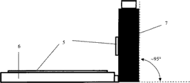
6、将第二源极管脚和漏极管脚形成的整体向上弯折、与引线框架垂直;6. Bending the whole formed by the second source pin and the drain pin upwards to be perpendicular to the lead frame;
7、将第二芯片的下端面通过导电胶与引线框架连接,固化成型。7. Connect the lower end surface of the second chip to the lead frame through conductive glue, and cure and form.
进一步,步骤3中,引线框架上包含两个向外引出第二源极管脚,将漏极管脚置于两个第二源极管脚之间。Further, in
或者,步骤3中,在引线框架上设置绝缘线、将引线框架分隔为第二源极和门极,门极向外引出门极管脚,第二源极向外引出第二源极管脚,将独立管脚置于门极管脚和第二源极管脚之间。Alternatively, in
或者,步骤1中,将第一芯片的下端面通过多个导电柱与预成型的漏极金属的上端面连接,第二芯片的上端面通过多个导电柱与所述的漏极金属的下端面连接;第一芯片的下端面还通过一绝缘立柱与一门极金属连接,第二芯片的上端面通过一导电柱与所述的门极金属连接,漏极金属与门极金属之间有间隙;Alternatively, in
步骤3中,引线框架的四个侧边均设有两个向外引出的第二源极管脚,每个侧边的两个源极管脚之间均放置一个独立管脚;In
步骤5中,将靠近门极金属的独立管脚上的暴露面通过导电胶与门极金属连接以形成门极管脚,将其余三个独立管脚上的暴露面通过导电胶与漏极金属连接以形成漏极管脚。In
本发明的技术构思是:将第二源极管脚和漏极管脚或门极管脚通过环氧模塑料塑封为一个整体,将此整体向上弯折直至与引线框架垂直,保证了三个管脚位于同一侧,从而使得经叠层封装的功率芯片可被直接应用,使用成本大大下降。The technical idea of the present invention is: the second source pin and the drain pin or the gate pin are molded into a whole through epoxy molding compound, and the whole is bent upward until it is perpendicular to the lead frame, ensuring three The pins are located on the same side, so that the stacked packaged power chip can be directly applied, and the cost of use is greatly reduced.
使暴露面或外露面的宽度大于管脚宽度,使得有足够的空间来调整引线位置。Make the width of the exposed or exposed side larger than the pin width so that there is enough room to adjust the lead position.
本发明具有源极、漏极和门极在封装结构的同一侧,可以直接应用,成本低廉的优点。The invention has the advantages that the source electrode, the drain electrode and the gate electrode are on the same side of the packaging structure, can be directly applied, and has low cost.
附图说明 Description of drawings
图1为本发明的示意图Fig. 1 is a schematic diagram of the present invention
图2为图1中的引线框架的展开图Figure 2 is an expanded view of the lead frame in Figure 1
图3为第一芯片的俯视图Figure 3 is a top view of the first chip
图4为第二芯片的俯视图Figure 4 is a top view of the second chip
图5a为第二种制作方法中的步骤1的第一芯片与漏极金属连接的示意图Figure 5a is a schematic diagram of the connection between the first chip and the drain metal in
图5a-1为图5a的俯视图Figure 5a-1 is a top view of Figure 5a
图5b为第一种制作方法中的步骤1的第二芯片与漏极金属连接的示意图Figure 5b is a schematic diagram of the connection between the second chip and the drain metal in
图5c为第一种制作方法中的步骤2的示意图Figure 5c is a schematic diagram of
图5d为第一种制作方法中的步骤3的示意图Figure 5d is a schematic diagram of
图5e为第一种制作方法中的步骤4的示意图Figure 5e is a schematic diagram of
图5f为第一种制作方法中的步骤5的示意图Figure 5f is a schematic diagram of
图5g为第一种制作方法中的步骤6的示意图Figure 5g is a schematic diagram of
图6为第二种制作方法中的步骤3的示意图Fig. 6 is the schematic diagram of
图7a为第三种制作方法中的步骤1的示意图Figure 7a is a schematic diagram of
图7a-1为图7a的A-A向剖视图Figure 7a-1 is a sectional view along the line A-A of Figure 7a
图7a-2为图7a的B-B向剖视图Figure 7a-2 is a cross-sectional view along the B-B direction of Figure 7a
图7b为第三种制作方法中的步骤3的示意图Figure 7b is a schematic diagram of
图7c为使用第三种制作方法制成的功率芯片的示意图Figure 7c is a schematic diagram of a power chip made using the third manufacturing method
图7c-1为图7c的C-C向示意图Figure 7c-1 is a schematic diagram of the C-C direction of Figure 7c
图7c-2为图7c的D-D向示意图Figure 7c-2 is a schematic diagram of the D-D direction of Figure 7c
具体实施方式 Detailed ways
实施例一Embodiment one
参照图1-5gRefer to Figure 1-5g
具有叠层封装预成型垂直结构的功率芯片,包括第一芯片2、第二芯片4,所述的第一芯片2位于第二芯片4之上,所述的第一芯片2和第二芯片4之间设有通过导体与两芯片2、4连接的漏极金属3,所述的第二芯片4通过导电胶5与一作为第二源极的、底部规则的引线框架6连接,所述的第一芯片2的上表面焊接有第一源极1;A power chip with a stacked packaging preformed vertical structure, including a
所述的引线框架6的侧边设有向外引出的第二源极管脚61,所述的第二源极管脚61与一漏极管脚31通过环氧模塑料塑封形成一个整体,所述的整体向上弯折、并与所述的引线框架6垂直;所述的漏极管脚31的中部设有一外露与所述的环氧模塑料的暴露面311,所述的暴露面通311过导电胶5与所述的漏极金属3连接。The side of the
所述的引线框架6的侧边向外引出两个第二源极管脚61,两个第二源极管脚61之间设置所述的漏极管脚31,三个管脚通过环氧模塑料塑封为所述的整体。Two second source pins 61 are drawn out from the side of the
所述的暴露面311的宽度大于所述的漏极管脚31的宽度。The width of the exposed
实施例二Embodiment two
参照附图1-4和图6Referring to accompanying drawings 1-4 and Figure 6
本实施例与实施例一的区别在于:所述的引线框架6上设有绝缘线10,所述的绝缘线10将所述的引线框架分隔为门极9和所述的第二源极,所述的门极9向外引出门极管脚91,所述的第二源极向外引出所述的第二源极管脚61,所述的门极管脚91和第二源极管脚61之间设置漏极管脚31,三个管脚通过环氧模塑料塑封为所述的整体。The difference between this embodiment and
其余相同。The rest is the same.
实施例3Example 3
参照图7a-7c-2Referring to Figure 7a-7c-2
本实施例与实施例一的区别之处在于:所述的第一芯片2的上表面焊接有第一门极92,所述的第一芯片2和第二芯片4之间设有门极金属93,所述的漏极金属3与门极金属31之间有间隙;所述的第一芯片2通过多个导电柱21与所述的漏极金属连接、通过一个绝缘立柱22与所述的门极金属93连接,所述的第二芯片4通过多个导电柱21与所述的漏极金属3连接、通过一个导电柱21与所述的门极金属93连接;所述的引线框架6的四个侧边均向外引出两个第二源极管脚61,其中一个侧边引出的两个第二源极管脚61之间设置门极管脚921,三个管脚通过环氧模塑料塑封为弯折向上的第一整体,所述的门极管脚921中部设有外露于环氧模塑料的外露面922,所述的外露面922通过导电胶与门极管脚921连接;其余三个侧面引出的两个第二源极管脚61之间放置所述的漏极管脚31。The difference between this embodiment and
所述的外露面922的宽度大于所述的门极管脚921的宽度。The width of the exposed
其余相同。The rest is the same.
实施例四Embodiment four
参照图1-5gRefer to Figure 1-5g
制造所述的具有叠层封装预成型垂直结构的功率芯片的方法,包括以下步骤:The method for manufacturing the power chip with a package-on-package preformed vertical structure includes the following steps:
1、将第一芯片的下端面与预成型的漏极金属的上端面连接,第一芯片的上端面焊接第一源极,将第二芯片与所述的漏极金属的下端面连接;1. Connect the lower end surface of the first chip to the upper end surface of the preformed drain metal, weld the first source to the upper end surface of the first chip, and connect the second chip to the lower end surface of the drain metal;
2、修剪漏极金属的形状,使其与所述的芯片适配;2. Trim the shape of the drain metal to fit the chip;
3、将底部规则的引线框架预先冲压成型,所述的引线框架上包含向外引出第二源极管脚,所述的第二源极管脚外侧设有装夹用的第一装夹杆;制作独立管脚,所述的独立管脚的一侧设有第二装夹杆;夹持所述的装夹杆用环氧模塑料通过模塑成型将第二源极管脚和独立管脚塑封为一整体,并在独立管脚中部放置一阻止环氧模塑料进入的阻隔块、以使独立管脚上形成一外露于环氧模塑料的暴露面;3. The lead frame with a regular bottom is pre-stamped and formed. The lead frame includes a second source pin that leads outwards, and a first clamping rod for clamping is provided on the outside of the second source pin ; Making independent pins, one side of the independent pins is provided with a second clamping rod; clamping the clamping rods with epoxy molding compound to mold the second source pins and independent tubes The foot is plastic-sealed as a whole, and a barrier block is placed in the middle of the independent pin to prevent the epoxy molding compound from entering, so that an exposed surface exposed to the epoxy molding compound is formed on the independent pin;
4、去除管脚上的装夹杆;4. Remove the clamping rod on the pin;
5、将独立管脚上的暴露面通过导电胶与漏极金属连接、形成漏极管脚;5. Connect the exposed surface of the independent pin to the drain metal through conductive glue to form a drain pin;
6、将第二源极管脚和漏极管脚形成的整体向上弯折、与引线框架垂直;6. Bending the whole formed by the second source pin and the drain pin upwards to be perpendicular to the lead frame;
7、将第二芯片的下端面通过导电胶与引线框架连接,固化成型。7. Connect the lower end surface of the second chip to the lead frame through conductive glue, and cure and form.
实施例五Embodiment five
参照图6Refer to Figure 6
本实施例与实施例三的区别之处在于:步骤3中,在引线框架上设置绝缘线、将引线框架分隔为第二源极和门极,门极向外引出门极管脚,第二源极向外引出第二源极管脚,将独立管脚置于门极管脚和第二源极管脚之间。The difference between this embodiment and the third embodiment is that: in
其余相同。The rest is the same.
实施例六Embodiment six
参照图7a-7c-2Referring to Figure 7a-7c-2
本实施例与实施例三的区别之处在于:步骤1中,将第一芯片的下端面通过多个导电柱与预成型的漏极金属的上端面连接,第二芯片的上端面通过多个导电柱与所述的漏极金属的下端面连接;第一芯片的下端面还通过一绝缘立柱与一门极金属连接,第二芯片的上端面通过一导电柱与所述的门极金属连接,漏极金属与门极金属之间有间隙;The difference between this embodiment and the third embodiment is that in
步骤3中,引线框架的四个侧边均设有两个向外引出的第二源极管脚,每个侧边的两个源极管脚之间均放置一个独立管脚;In
步骤5中,将靠近门极金属的独立管脚上的暴露面通过导电胶与门极金属连接以形成门极管脚,将其余三个独立管脚上的暴露面通过导电胶与漏极金属连接以形成漏极管脚。In
其余相同。The rest is the same.
本说明书实施例所述的内容仅仅是对发明构思的实现形式的列举,本发明的保护范围不应当被视为仅限于实施例所陈述的具体形式,本发明的保护范围也及于本领域技术人员根据本发明构思所能够想到的等同技术手段。The content described in the embodiments of this specification is only an enumeration of the implementation forms of the inventive concept. The protection scope of the present invention should not be regarded as limited to the specific forms stated in the embodiments. Equivalent technical means that a person can think of based on the concept of the present invention.
Claims (10)
Priority Applications (1)
| Application Number | Priority Date | Filing Date | Title |
|---|---|---|---|
| CN200910155097.2A CN101847622B (en) | 2009-12-23 | 2009-12-23 | Power chip with multi-stack package preformed vertical structure and manufacturing method thereof |
Applications Claiming Priority (1)
| Application Number | Priority Date | Filing Date | Title |
|---|---|---|---|
| CN200910155097.2A CN101847622B (en) | 2009-12-23 | 2009-12-23 | Power chip with multi-stack package preformed vertical structure and manufacturing method thereof |
Publications (2)
| Publication Number | Publication Date |
|---|---|
| CN101847622A CN101847622A (en) | 2010-09-29 |
| CN101847622B true CN101847622B (en) | 2012-01-25 |
Family
ID=42772165
Family Applications (1)
| Application Number | Title | Priority Date | Filing Date |
|---|---|---|---|
| CN200910155097.2A Expired - Fee Related CN101847622B (en) | 2009-12-23 | 2009-12-23 | Power chip with multi-stack package preformed vertical structure and manufacturing method thereof |
Country Status (1)
| Country | Link |
|---|---|
| CN (1) | CN101847622B (en) |
Families Citing this family (1)
| Publication number | Priority date | Publication date | Assignee | Title |
|---|---|---|---|---|
| CN110223966B (en) * | 2019-05-16 | 2021-05-07 | 宁波港波电子有限公司 | Lead frame and manufacturing method thereof |
Citations (2)
| Publication number | Priority date | Publication date | Assignee | Title |
|---|---|---|---|---|
| CN1677666A (en) * | 2004-03-31 | 2005-10-05 | 株式会社瑞萨科技 | Semiconductor device |
| CN101080816A (en) * | 2004-12-31 | 2007-11-28 | 万国半导体股份有限公司 | Flip chip contact(PCC) power package |
-
2009
- 2009-12-23 CN CN200910155097.2A patent/CN101847622B/en not_active Expired - Fee Related
Patent Citations (2)
| Publication number | Priority date | Publication date | Assignee | Title |
|---|---|---|---|---|
| CN1677666A (en) * | 2004-03-31 | 2005-10-05 | 株式会社瑞萨科技 | Semiconductor device |
| CN101080816A (en) * | 2004-12-31 | 2007-11-28 | 万国半导体股份有限公司 | Flip chip contact(PCC) power package |
Also Published As
| Publication number | Publication date |
|---|---|
| CN101847622A (en) | 2010-09-29 |
Similar Documents
| Publication | Publication Date | Title |
|---|---|---|
| CN102194788B (en) | Multi-layer lead frame package and method of fabrication | |
| US9824949B2 (en) | Packaging solutions for devices and systems comprising lateral GaN power transistors | |
| CN101656250B (en) | Compact co-packaged semiconductor dies with elevation-adaptive interconnection plates | |
| TWI411098B (en) | Power semiconductor package structure and method of manufacturing same | |
| CN101030570B (en) | Semiconductor device | |
| CN102655140B (en) | Multi-die package | |
| US20160268185A1 (en) | PACKAGING SOLUTIONS FOR DEVICES AND SYSTEMS COMPRISING LATERAL GaN POWER TRANSISTORS | |
| CN107978594B (en) | Electronic component package with heat spreader and multiple electronic components | |
| JP2013258387A (en) | Power-module semiconductor device | |
| US9362240B2 (en) | Electronic device | |
| CN102760724A (en) | Integrally-packaged power semiconductor device | |
| CN204102862U (en) | A multi-chip stack packaging device based on cavity technology | |
| CN107808868A (en) | Chip-packaging structure and its manufacture method | |
| CN103199075A (en) | Wafer-level semiconductor package structure with stacked chips and manufacturing method thereof | |
| CN201584411U (en) | Power chip with package-on-package preformed vertical structure | |
| CN101477973B (en) | Lead frame strip, sealing method thereof and sealing structure | |
| CN101847622B (en) | Power chip with multi-stack package preformed vertical structure and manufacturing method thereof | |
| CN105489578A (en) | Laminated chip packaging structure | |
| CN101894822B (en) | Lead frame band construction for semiconductor packaging | |
| TWM551755U (en) | Universal lead frame | |
| CN104022107A (en) | Electronic device | |
| CN104465597B (en) | A kind of four sides is without the flat package structure of semiconductor device of pin and method for packing | |
| CN106847713A (en) | Volume to volume makes the method and fan-out package structure of fan-out package structure | |
| CN223108881U (en) | A semiconductor packaging structure with dual packaging bodies | |
| CN214898401U (en) | Full packaging structure of power device |
Legal Events
| Date | Code | Title | Description |
|---|---|---|---|
| C06 | Publication | ||
| PB01 | Publication | ||
| C10 | Entry into substantive examination | ||
| SE01 | Entry into force of request for substantive examination | ||
| C14 | Grant of patent or utility model | ||
| GR01 | Patent grant | ||
| CF01 | Termination of patent right due to non-payment of annual fee |
Granted publication date: 20120125 |
|
| CF01 | Termination of patent right due to non-payment of annual fee |