CN101751356A - Method, system and apparatus for improving direct memory access transfer efficiency - Google Patents
Method, system and apparatus for improving direct memory access transfer efficiency Download PDFInfo
- Publication number
- CN101751356A CN101751356A CN200910222436A CN200910222436A CN101751356A CN 101751356 A CN101751356 A CN 101751356A CN 200910222436 A CN200910222436 A CN 200910222436A CN 200910222436 A CN200910222436 A CN 200910222436A CN 101751356 A CN101751356 A CN 101751356A
- Authority
- CN
- China
- Prior art keywords
- buffer
- dma
- memory access
- direct memory
- input
- Prior art date
- Legal status (The legal status is an assumption and is not a legal conclusion. Google has not performed a legal analysis and makes no representation as to the accuracy of the status listed.)
- Granted
Links
Images
Classifications
-
- G—PHYSICS
- G06—COMPUTING OR CALCULATING; COUNTING
- G06F—ELECTRIC DIGITAL DATA PROCESSING
- G06F13/00—Interconnection of, or transfer of information or other signals between, memories, input/output devices or central processing units
- G06F13/14—Handling requests for interconnection or transfer
- G06F13/20—Handling requests for interconnection or transfer for access to input/output bus
- G06F13/28—Handling requests for interconnection or transfer for access to input/output bus using burst mode transfer, e.g. direct memory access DMA, cycle steal
-
- G—PHYSICS
- G06—COMPUTING OR CALCULATING; COUNTING
- G06F—ELECTRIC DIGITAL DATA PROCESSING
- G06F12/00—Accessing, addressing or allocating within memory systems or architectures
-
- G—PHYSICS
- G06—COMPUTING OR CALCULATING; COUNTING
- G06F—ELECTRIC DIGITAL DATA PROCESSING
- G06F13/00—Interconnection of, or transfer of information or other signals between, memories, input/output devices or central processing units
- G06F13/14—Handling requests for interconnection or transfer
- G06F13/16—Handling requests for interconnection or transfer for access to memory bus
-
- G—PHYSICS
- G06—COMPUTING OR CALCULATING; COUNTING
- G06F—ELECTRIC DIGITAL DATA PROCESSING
- G06F5/00—Methods or arrangements for data conversion without changing the order or content of the data handled
Landscapes
- Engineering & Computer Science (AREA)
- Theoretical Computer Science (AREA)
- Physics & Mathematics (AREA)
- General Engineering & Computer Science (AREA)
- General Physics & Mathematics (AREA)
- Bus Control (AREA)
- Memory System Of A Hierarchy Structure (AREA)
Abstract
A mechanism is provided for improving the efficiency of multiple smaller direct memory access transfers. The mechanism uses one input buffer and a small result buffer, or some temporary variables, to temporarily store computation results. The mechanism performs a computation on a segment of data in the input buffer and stores the result in the temporary result buffer. The mechanism then copies the result back into the input buffer. As such, the mechanism uses the input buffer as both an input buffer and a results buffer. The mechanism then performs a direct memory access transfer on the segment of the input buffer that contains the computation result and then performs a computation on the next segment of the input buffer. The mechanism then repeats this process until the entire input buffer has been processed.
Description
Technical field
Improved data processing equipment of relate generally to of the present invention and method and relating more particularly to improved efficient that a plurality of less direct memory access (DMA) transmit so that at Cell wideband engine (CellBroadband Engine
TM) method and apparatus of programming on the processor.
Background technology
The Cell broadband engine architecture is the limited general purpose PowerArchitecture of performance for example
 Kernel and greatly quicken multimedia and streamlined coprocessing unit that vector handle to be used combines.The coprocessing unit is called as synergetic unit (SPE), and it significantly quickens the dedicated calculation of many forms.Cell wideband engine (Cell/B.E.
TM) processor is single-chip multi-core system structure, its be from computer game to a lot of compute-intensive applications in various applications, provide low cost and high-performance as the application of vast scopes such as geological data processing, bioinformatics, graphics process.Cell wideband engine and Cell/B.E. are that SCE is at the U.S., other countries or both trade marks.POWER ARCHITECTURE is that IBM Corporation is in the U.S., other countries or both registered trademarks.
Kernel and greatly quicken multimedia and streamlined coprocessing unit that vector handle to be used combines.The coprocessing unit is called as synergetic unit (SPE), and it significantly quickens the dedicated calculation of many forms.Cell wideband engine (Cell/B.E.
TM) processor is single-chip multi-core system structure, its be from computer game to a lot of compute-intensive applications in various applications, provide low cost and high-performance as the application of vast scopes such as geological data processing, bioinformatics, graphics process.Cell wideband engine and Cell/B.E. are that SCE is at the U.S., other countries or both trade marks.POWER ARCHITECTURE is that IBM Corporation is in the U.S., other countries or both registered trademarks.
Cell/B.E.
TMThe characteristic that architecture provides is for example to use eight synergetic unit (SPE), and each unit uses its oneself local reservoir (LS) rather than high-speed cache.This requires Cell/B.E.
TMThe programmer uses direct memory access (DMA) (DMA) instruction to transmit data and/or result between main shared storage and local reservoir clearly.This characteristic is Cell/B.E.
TMThe programmer provides higher dirigibility, has also brought more complicacy.
So, Cell/B.E.
TMThe programmer must consider to use the efficient of LS, and this influences the actual performance of application greatly.How using LS effectively is Cell/B.E.
TMThe important problems that the programmer should consider.Because each LS space is limited, it is ordinary frequently reciprocally carrying out the DMA transmission between primary memory and LS.Therefore, being used to carry out the strategy that DMA transmits may be crucial concerning using performance.
At present a kind of technology of generally using is called as " double buffering ".The basic thought of double buffering is to hide the DMA propagation delay by switch calculating between two buffer memorys, carries out calculating thus when carrying out DMA on buffer memory therein and transmit on another buffer memory.For compute-bound application, this technology can be hidden the DMA propagation delay effectively.
Yet it is memory-bound that a lot of application are arranged, and the performance of using under those situations is not the restriction that is subjected to the computing power of each SPE, but is subjected to the restriction of DMA transmission bandwidth.Therefore, may there be adverse influence any time of expending in the DMA transmission to the performance of using.In order to obtain more performance and efficient, the programmer can carry out the least possible DMA with big as far as possible transmission size as far as possible and transmit.Yet,, make double buffering become the unique technical of improving performance because the character of a lot of computational algorithms possibly can't avoid a plurality of less DMA to transmit.
Summary of the invention
In one exemplary embodiment, provide a kind of method that improved direct memory access (DMA) transmits that in data handling system, is used for.Method comprises that carrying out direct memory access (DMA) transmits so that data are loaded into input-buffer from primary memory, first data segment in the input-buffer is carried out at least one to be calculated to produce the first result data section, the first result data section deposited get back in the input-buffer, and initiate direct memory access (DMA) and transmit to store the first result data section into primary memory from input-buffer.
In another exemplary embodiment, provide a kind of and comprise that computing machine can be used or the computer program of computer-readable recording medium, but this medium has the computing machine logging program.When computer-readable program is performed on calculation element, make calculation element carry out one of above-mentioned various operations about the method exemplary embodiment or its combination.
In another exemplary embodiment, provide a kind of systems/devices.Systems/devices can comprise one or more processors and the storer that is connected to these one or more processors.Storer can comprise instruction, when this instruction is carried out by one or more processors, makes one or more processors carry out one of above-mentioned various operations about the method exemplary embodiment or its combination.
These and other characteristic of the present invention and advantage will be described in following detailed description to exemplary embodiment of the present, and perhaps those of ordinary skill in the art will understand these and other characteristic and advantage of the present invention after reading.
Description of drawings
The present invention, and preferred use-pattern and further purpose and advantage can get the best understanding by the reference accompanying drawing and with reference to following detailed description to exemplary embodiment of the present.
Fig. 1 is the example block diagram that wherein can realize the data handling system of various aspects of the present invention;
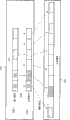
Fig. 2 shows the direct memory access (DMA) tranmission techniques;
Fig. 3 shows the direct memory access (DMA) tranmission techniques that uses double buffering;
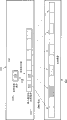
Fig. 4 shows the direct memory access (DMA) tranmission techniques according to the interim result cache of use of an exemplary embodiment;
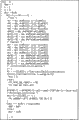
Fig. 5 A and Fig. 5 B show the example of the code that uses the direct memory access (DMA) transmission, and wherein direct memory access (DMA) transmits and uses double buffering;
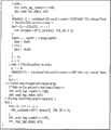
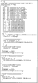
Fig. 6 shows the example according to the code of the use direct memory access (DMA) transmission of an exemplary embodiment, and wherein direct memory access (DMA) transmits and uses temporary variable;
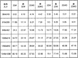
Fig. 7 is the table to the improvement in performance of various matrix size and calculating that illustrates according to an exemplary embodiment; And
Fig. 8 is the process flow diagram that illustrates according to the direct memory access (DMA) transfer operation of an interim result cache of exemplary embodiment utilization.
Embodiment
Exemplary embodiment is provided for improving the mechanism of the efficient that a plurality of less direct memory access (DMA) transmit.This mechanism can be used for double buffering technology applied any application usually.This mechanism uses an input-buffer and little result cache or some temporary variables with storage computation result provisionally.This mechanism is carried out the data segment in the input-buffer and is calculated and result or intermediate result are stored in result cache or the temporary variable.This mechanism is duplicated the result subsequently and is fed back into buffer memory or directly the result is stored in the input-buffer.Like this, this mechanism with input-buffer both as input-buffer also as a result of buffer memory used.
This mechanism is carried out to the section of the input-buffer that comprises result of calculation that direct memory access (DMA) transmits subsequently and subsequently next section execution of input-buffer is calculated.This mechanism repeats this process subsequently till whole input-buffer is processed.This mechanism is not carried out the direct memory access (DMA) status checking during calculating and direct memory access (DMA) transport process.This mechanism only checks just when it need reuse input-buffer whether the direct memory access (DMA) transmission is finished.
This mechanism is carried out extra replicate run in local reservoir; Yet the expense of duplicating in local reservoir is finished less than the direct memory access (DMA) delivery status being checked and waited for direct memory access (DMA) transmits.In fact, this mechanism can not carried out extra duplicating because for some negative assorted calculating, this mechanism can use simply interim buffer memory with storage intermediate result and directly net result is put back to input-buffer rather than interim result cache in.Therefore, this mechanism is not only used limited less local reservoir space, also brings more performance.
Exemplary embodiment can be utilized in many data of different types processing environments, comprises distributed data processing environment, individual data treatment facility etc.For discrete cell and functional description of giving exemplary embodiment provides background, provide Fig. 1 at this as exemplary environments, each illustrative aspects that therein can realization example embodiment.Description to Fig. 1 will mainly concentrate on individual data treatment facility embodiment, but this is exemplary and and is not intended to any restriction to relevant characteristic of the present invention of statement or hint.On the contrary, exemplary embodiment is intended to comprise distributed data processing environment, grid computing environment or the like.
Fig. 1 is the example block diagram that wherein can realize the data handling system of various aspects of the present invention.Example data disposal system shown in Fig. 1 is Cell wideband engine (Cell/B.E.
TM) example of data handling system.Although Cell/B.E.
TMProcessor will use in description of the preferred embodiment of the present invention, but those of ordinary skill in the art can understand after reading following description, and the present invention is not limited to this.
As shown in Figure 1, Cell/B.E.
TMProcessor 100 comprises main processor unit (PPE) 110, and it has processor (PPU) 116 and L1 high-speed cache 112 and L2 high-speed cache 114; And a plurality of coprocessors unit (SPE) 120 to 134, it has oneself coprocessor unit (SPU) 140 to 154, memory stream control 155 to 162, local storage or reservoir (LS) 163 to 170 and Bus Interface Unit (BIU unit) 180 to 194 respectively, and Bus Interface Unit can be for example to make up direct memory access (DMA) (DMA), Memory Management Unit (MMU) and Bus Interface Unit.And provide high bandwidth internal element interconnection (EIB) 196, bus interface controller (BIC) 197 and memory interface controller (MIC) 198.
Local storage or local reservoir (LS) 163 to 170 are incoherent addressable parts of large memories mapping, and it physically can be used as the small memory that is connected to SPU 140 to 154 and provides.Local reservoir 163 to 170 can be mapped to different address spaces.These address areas are continuous in non-aliasing configuration.Local reservoir 163 to 170 by its address location for example via hereinafter its corresponding SPU 149 to 154 of SPU identification register discussed in detail and SPE 120 to 134 are associated.As long as local reservoir is not under the security mode of operation, any resource in the system all have the ability from/to local reservoir 163 to 170 read/write, the SPU that only local reservoir is associated under security mode of operation can visit the security of the appointment of local reservoir 163 to 170 or local reservoir 163 to 170.
Cell/B.E.
TMProcessor 100 can be a System on Chip/SoC, and making to provide each unit shown in Fig. 1 on single microprocessor chip.And, Cell/B.E.
TMProcessor 100 is heterogeneous processing environment, and wherein each SPU can receive different instruction by each other SPU from system.And the instruction set of SPU is different with the instruction set of PPU, and for example, PPU can carry out based on the instruction of Reduced Instruction Set Computer (RISC) and SPU carries out the vector quantization instruction.
SPE 120 to 134 is connected to each other via EIB 196 and is connected to L2 high-speed cache 114.In addition, SPE 120 to 134 is connected to MIC 198 and BIC 197 via EIB 196.MIC 198 provides communication interface to shared storage 199.BIC 197 is at Cell/B.E.
TMProvide communication interface between processor 100 and other external buss and the device.
PPE 110 is two-wire journey PPE 110.The combination of two-wire journey PPE 110 and eight SPE 120 to 134 makes Cell/B.E.
TM100 can handle 10 concurrent threads and not finish memory requests above 128.PPE 110 is as the controller of other eight SPE 120 to 134 that handle most of amount of calculation.For example PPE 110 can be used to move legacy operating system and the execution of SPE 120 to 134 execution vector quantization floating-point codes.
SPE 120 to 134 comprises synergetic unit (SPU) 140 to 154, memory stream control 155 to 162, local storage or reservoir 163 to 170 and interface unit 180 to 194.In one exemplary embodiment, local storage or reservoir 163 to 170 comprise 256KB instruction and data storer, and it is visible and can be by directly addressing of software for PPE 110.
PPE 110 can load small routine or thread to SPE 120 to 134, and SPE is linked to together to handle each step in the complex operations.For example, can load the program that is used to read DVD, video and audio decoder and demonstration, and data can pass to SPE until its final Output Display Unit that arrives from SPE in conjunction with the set-top box of CBE 100.At 4GHz, each SPE 120 to 134 provides the performance of the 32GFlops of theory, and PPE 110 has the similar performance level.
Memory stream control module (MFC) 155 to 162 is as the interface of SPU to system all the other and other unit.MFC 155 to 162 transmits, protects and provide synchronously fundamental mechanism for data between main memory and the local reservoir 163 to 170.Each SPU has MFC on processor in logic.Some embodiment can share the resource of a MFC between a plurality of SPU.In this case, whole instruments and the order for the MFC definition must show the software that is independent of each SPU.The effect of sharing MFC is limited to instrument and the order that depends on realization.
Fig. 2 shows the direct memory access (DMA) tranmission techniques.Synergetic unit (SPE) 210 is carried out direct memory access (DMA) (DMA) and is transmitted so that data are loaded into input-buffer 220 from primary memory 250.SPE 210 carries out the data segment in the buffer memory 220 subsequently and calculates and the result is stored in the result cache 230.For example, 210 pairs of data segments of SPE 222 are carried out and are calculated to bear results data segment 232 and data segment 224 carried out calculate with the data segment 234 that bears results.Input-buffer 220 and result cache 230 can be the parts of the local reservoir that is associated with SPE 210.For example, SPE 210 can be one of SPE 120 to 134, and input-buffer 220 and result cache 230 are included in one of local reservoir (LS) 163 to 170 among Fig. 1.
In the example shown in Fig. 2, SPE 210 carries out DMA subsequently and transmits so that the result is sent to the primary memory 250 from result cache 230.SPE 210 can be sent to the diverse location primary memory so that be the calculating preparation data of next step from result cache 230 with the result data section.Therefore, SPE 210 can carry out a plurality of less DMA and transmits or use and comprise that from result cache 230 to primary memory the DMA tabulation that 250 a plurality of less DMA transmits carries out a dma operation.All will use relatively large result cache in both cases.
Cell/B.E.
TMThe programmer must consider to use the efficient of LS, and this influences the actual performance of application greatly.How using LS effectively is Cell/B.E.
TMThe important problems that the programmer should consider.Because the space of each LS is limited, it is ordinary frequently reciprocally carrying out the DMA transmission between primary memory and LS.Therefore, being used to carry out the strategy that DMA transmits may be crucial concerning using performance.
The technology of generally using is called " double buffering " at present.The basic thought of double buffering is to hide the DMA propagation delay by switch calculating between two buffer memorys, carries out calculating thus when carrying out DMA on buffer memory therein and transmit on another buffer memory.For compute-bound application, this technology can be hidden the DMA propagation delay effectively.
Fig. 3 shows the direct memory access (DMA) tranmission techniques that uses double buffering.SPE 310 carries out DMA and transmits so that data are loaded into input-buffer 320 from primary memory 350.SPE 310 carries out the data segment in the input-buffer 320 subsequently and calculates.In the example that illustrates, SPE 310 alternately stores the result among result cache A 330 and the result cache B 340 into.For example, 310 pairs of data segments of SPE 322 are carried out and are calculated to be created in the result data section 332 among the input-buffer A 330 and data segment 324 to be carried out calculate to be created in the result data section 334 among the input-buffer B 340.
In the example shown in Fig. 3, SPE 310 carries out DMA subsequently and transmits so that the result is stored into the primary memory 350 from result cache A 330 and result cache B 340.SPE 310 can store the result data section diverse location of primary memory 350 into so that be the calculating preparation data of next step from result cache A 330 and result cache B 340.SPE 310 alternately, carries out data segment and to calculate and the result is stored in the result cache and to carry out DMA simultaneously and transmit with the result data section of storage from another result cache between result cache A 330 and result cache B 340.For example, SPE 310 can carry out data segment 324 and calculate and result data section 344 is stored among the result cache B 340 and carry out DMA simultaneously and transmit storing primary memory 350 into from the result data section 332 of result cache A 330.Subsequently, SPE 310 can carry out next calculating and the result is stored among the result cache A and carries out DMA simultaneously and transmit and will store primary memory 350 into from the result data section 344 of result cache B 340 next data segment.Thus, SPE 310 carries out a plurality of less DMA transmission from result cache A 330 and result cache B 340 to primary memory.
It is memory-bound that a lot of application are arranged, and the performance of using under those situations is not limited to the computing power of each SPE, but is subject to the DMS transmission bandwidth.In addition, double buffering shortcoming is that SPE must check the state of DMA transmission and reuse buffer memory and if only if Shi Caineng is finished in the DMA transmission.This causes synchronous overhead.Therefore, according to exemplary embodiment, provide a kind of mechanism that is used to improve the efficient that a plurality of less direct memory access (DMA) transmit.This mechanism can be used for double buffering technology applied any application usually.
Fig. 4 shows the direct memory access (DMA) tranmission techniques according to the interim result cache of use of an exemplary embodiment.SPE 410 comprises input and result cache 420 and interim result cache 430.SPE 410 carries out DMA and transmits so that data are loaded into input-buffer 420 from primary memory 450.SPE 410 carries out the data segment in the input-buffer 420 subsequently and calculates.In the example that illustrates, 410 pairs of data segments of SPE 424 are carried out and are calculated and provisionally result or intermediate result are stored in the result data section 434 of interim result cache 430.Interim result cache 430 can be the sub-fraction of local reservoir or the one or more registers in SPE 410.SPE 410 subsequently with result data section 434 from interim result cache 430 duplicate be fed back into result cache 420 or the data segment 434 that comprises intermediate result carried out another calculating and the result put into input and result cache 420.
In the example shown in Fig. 4, SPE 410 carries out DMA subsequently and transmits so that the result is stored into the primary memory 450 from input and result cache 420.Because the algorithm realized or in order to prepare to be used for the data of the calculating of next step, SPE 410 can be sent to diverse location the primary memory 450 from input and result cache 420 with the result data section.SPE 410 can carry out calculating to a data segment such as data segment 424, and result's storage is fed back into and result cache 420, transmits to store last result data section such as data segment 422 into primary memory 450 from input and result cache 420 and carry out DMA simultaneously.Thus, SPE 410 can carry out a plurality of less DMA transmission to primary memory 450 from input and result cache 420.
SPE 410 repeats this process subsequently till whole input-buffer is processed.SPE410 does not carry out the direct memory access (DMA) status checking during calculating and direct memory access (DMA) transport process.SPE 410 only checks just when it need reuse input and result cache 420 whether the direct memory access (DMA) transmission is finished.SPE 410 carries out extra replicate run in local reservoir; Yet the expense of duplicating in local reservoir is finished less than the direct memory access (DMA) delivery status being checked and waited for direct memory access (DMA) transmits.In fact, SPE 410 can carry out extra duplicating because for some complicated calculations, SPE 410 can simply the result be put back in the input-buffer rather than interim result cache in.Therefore, the DMA of the interim result cache of use as shown in Figure 4 transmits and not only uses limited less local reservoir space, also brings more performance.
Persons of ordinary skill in the art may appreciate that the present invention can be used as system, method or computer program and realizes.Correspondingly, the present invention can take hardware embodiment completely, completely software implementation example (comprising firmware, resident software, microcode etc.) or usually can be called as in this manual " circuit ", " module " or " system " combination the form of embodiment of software and hardware aspect.And then the present invention can take the form of the computer program that comprises in any tangible medium of expressing, and it has the computer readable program code that comprises in medium.
Can adopt one or more computing machines can with or the combination in any of computer-readable medium.Computing machine can with or computer-readable medium can be, such as but not limited to electronics, magnetic, optics, electromagnetism, infrared or semi-conductive system, device, equipment or propagation medium.The how specific example of computer-readable medium (enumerating of non-limit) can comprise: medium or magnetic storage apparatus with electrical connection, portable computer diskette, hard disk, random-access memory (ram), ROM (read-only memory) (ROM), Erasable Programmable Read Only Memory EPROM (EPROM or flash memory), optical fiber, portable compact disk ROM (read-only memory) (CDROM), optical storage apparatus, transfer medium such as those support the Internets or Intranet of one or more wiring.Note computing machine can with or computer-readable medium even can be paper or another kind of suitable medium, be printed with program on it, because if need, program can be obtained electronically via for example optical scanning to paper or other media, subsequently by editor, the translation or do other processing by rights, be stored in the computer memory subsequently.Under this instructions background, computing machine can with or computer-readable medium can be can comprise, storage, transmission, propagation or transmission procedure used or united with it use for instruction execution system, device or equipment any medium.Computer usable medium can comprise the propagation data signal, comprises computer usable program code in the signal in the part of base band or carrier wave.Computer usable program code can use any suitable medium to be transmitted, and includes but not limited to: wireless, wired, optical cable, radio frequency (RF) etc.
Be used to realize that the computer program code of operation of the present invention can be write as the combination in any of one or more programming languages, comprise object-oriented programming language such as Java
TM, Smalltalk
TM, C++ etc. and traditional process procedures design language be as " C " programming language or similar programming language.Program code can fully carried out on the subscriber computer, partly carry out on the subscriber computer, carrying out, partly carrying out on the remote computer or fully carrying out on the remote computer or on the server on the subscriber computer and partly as the stand alone software bag.Under latter event, remote computer can be connected to subscriber computer by the network (comprising Local Area Network or wide area network (WAN)) of any kind, perhaps can be connected to outer computer (for example, by using the ISP because of the special envoy).
Following reference is described exemplary embodiment according to the process flow diagram and/or the block scheme of method, device (system) and the computer program of exemplary embodiment of the present invention.Be appreciated that each frame in process flow diagram and/or the block scheme or the combination of the frame in process flow diagram and/or the block scheme can be realized by computer program instructions.These computer program instructions can be provided for the processor of general purpose computing machine, specific purpose computing machine or other programmable data treating apparatus to produce machine, make call instruction when carrying out, produce the device of the function/action of a frame being used for realization flow figure and/or block scheme or a plurality of frame defineds via the processor of computing machine or other programmable data treating apparatus.
These computer program instructions also can be stored in and can instruct computing machine or other programmable data treating apparatus to bring into play in a particular manner in the computer-readable medium of function, make the instruction be stored in the computer-readable medium produce a kind of goods, it comprises the command device of the function/action of a frame in realization flow figure and/or the block scheme or a plurality of frame defineds.
Computer program instructions also can be loaded on computing machine or other programmable data treating apparatus, so that on computing machine or other programmable data treating apparatus, carry out a series of exercisable steps, to produce computer implemented process, make the instruction of carrying out at computing machine or other programmable data treating apparatus be provided for the process of the function/action of a frame in realization flow figure and/or the block scheme or a plurality of frame defineds.
Process flow diagram in the accompanying drawing and block scheme illustrate the architecture of the possible embodiment of according to various embodiments of the present invention system, method and computer program product, functional and operation.Thus, each frame can representative code in process flow diagram and/or the block scheme module, section or part, it comprises the one or more executable instructions that are used to realize specific logical function.Should be noted that at some alternative Shi Lizhong, the function of indicating in the frame can according to different the occurring in sequence of diagram.For example, two frames shown in the order perhaps sometimes can be carried out with opposite order according to functionally in fact can side by side carrying out basically of relating to.Also should be noted that, each frame in process flow diagram and/or the block scheme, and the combination of the frame in process flow diagram and/or the block scheme, can be by execution specific function or the hardware based specific purpose system of action or the combination realization of specific purpose hardware and computer instruction.
Fig. 5 A and Fig. 5 B show the example of the code that uses the direct memory access (DMA) transmission, and wherein direct memory access (DMA) transmits and uses double buffering.Code shown in Fig. 5 A and Fig. 5 B shows and is used for Cell/B.E.
TMThe parallel prime factor of architecture is analyzed fast fourier transform (PFAFFT).Fig. 6 shows the example according to the code of the use direct memory access (DMA) transmission of an exemplary embodiment, and wherein direct memory access (DMA) transmits and uses interim buffer memory.Code shown in Figure 6 is carried out and is used for Cell/B.E.
TMThe same parallel PFAFFT function of architecture, and the code among Fig. 6 is not only more effective but also more brief.It is big more that the long more and little DMA of input-buffer transmits quantity, and improvement in performance is big more.
Fig. 7 is the table that illustrates according to the improvement in performance of the various matrix size of an exemplary embodiment and calculating.For every kind of matrix size and calculating, the table shown in Fig. 7 has compared time and corresponding " newly " time that is used to use double buffering calculating, and wherein " newly " time is used routine input/result cache as shown in Figure 4 and interim result cache.
At Cell/B.E.
TMThe realization of two kinds of PFAFFT is arranged on the data handling system, and they use different strategies: a kind of is that " 3 step PFAFFT " and another kind are " 2 step PFAFFT ".And two kinds of situations of using PFAFFT are also arranged: a kind of is that to adopt the input data of vector quantization form and another kind be the input data of the non-vector quantization form of employing.For latter event, PFAFFT need be the vector quantization form from non-vector quantization format conversion with the input data, and carrying out FFT calculating subsequently and needing output data after FFT calculates is non-vector quantization form from the vector quantization format conversion.3 step PFAFFT of vector quantization input data are adopted in " 3SW " representative.3 step PFAFFT of vector quantization input data are not adopted in " 3SWO " representative." 2SW " representative adopt 2 step PFAFFT of vector quantization input data and similarly " 2SWO " representative do not adopt 2 step PFAFFT of vector quantization input data.
Fig. 8 illustrates the process flow diagram that adopts the direct memory access (DMA) transfer operation of interim result cache device according to an exemplary embodiment.Operation beginning, this mechanism are carried out direct memory access (DMA) (DMA) transmission data are loaded into input-buffer (frame 802) from primary memory.This mechanism is carried out the data segment in the input-buffer subsequently and is calculated (frame 804) and the result is stored in (frame 806) in the interim result cache.Subsequently, this mechanism is duplicated the result and is fed back into (frame 808) in the buffer memory.Therefore, this mechanism with input-buffer both as input-buffer also as a result of buffer memory use.In an alternate embodiment, perhaps when calculate allowing, this mechanism also can directly be deposited the result and be got back in input/result cache and do not use interim result cache.
Next, this mechanism is sent to primary memory (frame 810) with section as a result.This mechanism determines whether that the section as a result that is transmitted is last section (frame 812) in the input-buffer.If this section is not last section, operation is got back to frame 804 and is calculated so that next data segment is carried out.Transmission in the frame 810 is that DMA transmits.Therefore, when the DMA in the frame 810 was transmitted in execution, this mechanism can be carried out next calculating concurrently.Only to last calculating, this mechanism must be checked the state of the DMA transmission of getting back to primary memory.
If in frame 812, the section in the input-buffer is last section, and this mechanism determines whether it needs to reuse input-buffer (frame 814).If should mechanism not need to reuse input-buffer, EO.At frame 814, need reuse input-buffer if should mechanism determine it, this mechanism is checked the state (frame 816) that DMA transmits and is determined whether that all DMA transmission from input/result cache to primary memory finish (frame 818).If all DMA transmit and finish, operation is got back to frame 802 and is transmitted with the next DMA that carries out from the primary memory to the input-buffer.Otherwise operation is got back to frame 816 and is checked the state that DMA transmits.
Therefore, exemplary embodiment is provided for improving the mechanism of the efficient that a plurality of less direct memory access (DMA) transmit.This mechanism can be used for double buffering technology applied any application usually.This mechanism uses an input-buffer and little result cache or some temporary variables with storage computation result provisionally.This mechanism is carried out the data segment in the input-buffer and is calculated and the result is stored in the interim result cache.This mechanism is duplicated the result subsequently and is fed back in the buffer memory.Like this, this mechanism with input-buffer both as input-buffer also as a result of buffer memory use.
This mechanism is carried out to the section of the input-buffer that comprises result of calculation that direct memory access (DMA) transmits subsequently and subsequently (calculate and the direct memory access (DMA) transmission will side by side be carried out) is calculated in next section execution of input-buffer.This mechanism repeats this process subsequently till whole input-buffer is processed.This mechanism is not carried out the direct memory access (DMA) status checking during calculating and direct memory access (DMA) transport process.This mechanism only checks just when it need reuse input-buffer whether the direct memory access (DMA) transmission is finished.This mechanism is carried out extra replicate run in local reservoir; Yet the expense of duplicating in local reservoir is finished less than the direct memory access (DMA) delivery status being checked and waited for direct memory access (DMA) transmits.
As mentioned above, should be appreciated that exemplary embodiment can take completely hardware embodiment, software implementation example or both comprised that hardware cell also comprised the form of the embodiment of software unit completely.In the example of an embodiment, the mechanism of exemplary embodiment realizes that with software or program code it includes but not limited to firmware, resident software, microcode etc.
Be suitable for storing and/or the data handling system of executive routine code will comprise directly or be connected to indirectly by system bus at least one processor of memory cell.Memory cell can be included in local storage, mass storage and the high-speed cache that program code utilizes actual the term of execution, and high-speed cache is must be from the number of times of large capacity cache retrieval coding in order to be reduced in the term of execution and the interim storage space that provides at least some program codes.
I/O or I/O equipment (including but not limited to keyboard, display, indicating equipment etc.) can be directly or are connected to system by I/O controller between two parties.Network adapter also can be connected to system to allow data handling system by individual or public network are connected to other data handling systems or remote printer or memory device between two parties.Several in the just at present available types of network adapters of modulator-demodular unit, cable modem and Ethernet card.
The description of this invention is to provide for the purpose of explaining and describing, and is not intended to disclosed form limit or restriction the present invention.Those having ordinary skill in the art will appreciate that many changes and modification.To the selection of embodiment and description is for best interpretations is made in principle of the present invention, practical application, and in order to make those of ordinary skill in the art understand various changes that are suitable for the special-purpose of being expected to various embodiments of the invention.
Claims (14)
1. one kind is used for the method that improved direct memory access (DMA) transmits in data handling system, and described method comprises:
Carrying out direct memory access (DMA) transmits so that data are loaded into input-buffer from primary memory;
First data segment in the described input-buffer is carried out at least one to be calculated to produce the first result data section;
The described first result data section deposited get back in the described input-buffer; And
Initiating direct memory access (DMA) transmits to store the described first result data section into described primary memory from described input-buffer.
2. method according to claim 1, wherein the described first result data section is stored back described input-buffer and comprise:
The described first result data section is stored in the interim result cache; And
The described first result data section is copied to the described input-buffer from described interim result cache.
3. method according to claim 2, wherein said interim result cache and described input-buffer are stored in the local reservoir that is associated with synergetic unit.
4. method according to claim 2, wherein said interim result cache comprises one or more registers.
5. method according to claim 1 further comprises:
With last result data section is transmitted concurrently from the direct memory access (DMA) that described input-buffer stores described primary memory into, the current data section is carried out at least one calculates to produce the current results data segment.
6. method according to claim 5 further comprises:
Described current results data segment deposited get back in the described input-buffer; And
Initiating direct memory access (DMA) transmits to store described current results data segment into described primary memory from described input-buffer.
7. method according to claim 6 further comprises:
In response to described current data section is last data segment in the described input-buffer, determines whether to reuse described input-buffer.
8. method according to claim 7 further comprises:
To reuse described input-buffer in response to determining, check to be used to store the state that the direct memory access (DMA) of result data section before this transmits; And
Transmit in response to the be useful on direct memory access (DMA) of storing result data section before this and to have finished, carry out direct memory access (DMA) and transmit so that follow-up data is loaded into described input-buffer from described primary memory.
9. a computer program that comprises computer-readable medium records computer-readable program on the described medium, wherein when described computer-readable program is performed on calculation element, makes described calculation element realize arbitrary method of claim 1 to 8.
10. computer system comprises the device of the arbitrary method that is used to realize claim 1 to 8.
11. a device comprises:
Processor; And
Be connected to the storer of described processor, wherein said storer comprises instruction, when described instruction is carried out by described processor, makes processor:
Carrying out direct memory access (DMA) transmits so that data are loaded into input-buffer from primary memory;
First data segment in the described input-buffer is carried out at least one to be calculated to produce the first result data section;
The described first result data section deposited get back in the described input-buffer; And
Initiating direct memory access (DMA) transmits to store the described first result data section into described primary memory from described input-buffer.
12. device according to claim 11 is wherein stored back described input-buffer with the described first result data section and is comprised:
The described first result data section is stored in the interim result cache; And
The described first result data section is copied to the described input-buffer from described interim result cache.
13. device according to claim 11, wherein said instruction further makes processor:
With last result data section is transmitted concurrently from the direct memory access (DMA) that described input-buffer stores described primary memory into, the current data section is carried out at least one calculates to produce the current results data segment;
Described current results data segment is deposited back in the described input-buffer; And
Initiating direct memory access (DMA) transmits to store described current results data segment into described primary memory from described input-buffer.
14. device according to claim 13, wherein said instruction further makes processor:
In response to described current data section is last data segment in the described input-buffer, determines whether to reuse described input-buffer;
To reuse described input-buffer in response to determining, check to be used to store the state that the direct memory access (DMA) of result data section before this transmits; And
Transmit in response to the be useful on direct memory access (DMA) of storing result data section before this and to have finished, carry out direct memory access (DMA) and transmit so that follow-up data is loaded into described input-buffer from described primary memory.
Applications Claiming Priority (2)
| Application Number | Priority Date | Filing Date | Title |
|---|---|---|---|
| US12/337,703 US8412862B2 (en) | 2008-12-18 | 2008-12-18 | Direct memory access transfer efficiency |
| US12/337,703 | 2008-12-18 |
Publications (2)
| Publication Number | Publication Date |
|---|---|
| CN101751356A true CN101751356A (en) | 2010-06-23 |
| CN101751356B CN101751356B (en) | 2012-08-22 |
Family
ID=42267771
Family Applications (1)
| Application Number | Title | Priority Date | Filing Date |
|---|---|---|---|
| CN2009102224364A Expired - Fee Related CN101751356B (en) | 2008-12-18 | 2009-11-13 | Method, system and apparatus for improving direct memory access transfer efficiency |
Country Status (4)
| Country | Link |
|---|---|
| US (1) | US8412862B2 (en) |
| JP (1) | JP5528054B2 (en) |
| KR (1) | KR20100070981A (en) |
| CN (1) | CN101751356B (en) |
Cited By (2)
| Publication number | Priority date | Publication date | Assignee | Title |
|---|---|---|---|---|
| CN102880472A (en) * | 2012-09-28 | 2013-01-16 | 方正国际软件有限公司 | System for data access in process engine |
| CN103490854A (en) * | 2013-09-03 | 2014-01-01 | 华为技术有限公司 | Training window adding method and chip |
Families Citing this family (5)
| Publication number | Priority date | Publication date | Assignee | Title |
|---|---|---|---|---|
| JP2012031052A (en) | 2010-06-28 | 2012-02-16 | Asahi Glass Co Ltd | Method for producing glass body and method for producing optical member for euv lithography |
| CN105677592A (en) * | 2015-12-31 | 2016-06-15 | 北京经纬恒润科技有限公司 | Bus communication method and system |
| US12282683B2 (en) | 2019-03-12 | 2025-04-22 | Intel Corporation | Computational data storage systems |
| US12260127B2 (en) | 2020-12-23 | 2025-03-25 | Intel Corporation | Technologies for storage and processing for distributed file systems |
| US12353744B2 (en) * | 2022-01-14 | 2025-07-08 | SanDisk Technologies, Inc. | Cold storage partition management in proof of space blockchain systems |
Family Cites Families (17)
| Publication number | Priority date | Publication date | Assignee | Title |
|---|---|---|---|---|
| US6397316B2 (en) | 1997-07-24 | 2002-05-28 | Intel Corporation | System for reducing bus overhead for communication with a network interface |
| JP3289661B2 (en) * | 1997-11-07 | 2002-06-10 | 日本電気株式会社 | Cache memory system |
| US6484251B1 (en) * | 1999-10-14 | 2002-11-19 | International Business Machines Corporation | Updating condition status register based on instruction specific modification information in set/clear pair upon instruction commit in out-of-order processor |
| US6681273B1 (en) * | 2000-08-31 | 2004-01-20 | Analog Devices, Inc. | High performance, variable data width FIFO buffer |
| JP3878508B2 (en) * | 2001-11-08 | 2007-02-07 | 松下電器産業株式会社 | Circuit group control system |
| EP1454460A1 (en) * | 2001-11-13 | 2004-09-08 | Transwitch Corporation | Overcoming access latency inefficiency in memories for packet switched networks |
| JP3934493B2 (en) * | 2002-06-28 | 2007-06-20 | 富士通株式会社 | Integrated circuit and system development method |
| US7114042B2 (en) | 2003-05-22 | 2006-09-26 | International Business Machines Corporation | Method to provide atomic update primitives in an asymmetric heterogeneous multiprocessor environment |
| US7177982B2 (en) | 2004-01-16 | 2007-02-13 | International Business Machines Corporation | Method to maintain order between multiple queues with different ordering requirements in a high frequency system |
| US20060090016A1 (en) * | 2004-10-27 | 2006-04-27 | Edirisooriya Samantha J | Mechanism to pull data into a processor cache |
| US7447868B2 (en) * | 2005-06-15 | 2008-11-04 | International Business Machines Corporation | Using vector processors to accelerate cache lookups |
| US7398368B2 (en) | 2005-12-01 | 2008-07-08 | Sony Computer Entertainment Inc. | Atomic operation involving processors with different memory transfer operation sizes |
| US7870544B2 (en) | 2006-04-05 | 2011-01-11 | International Business Machines Corporation | Insuring maximum code motion of accesses to DMA buffers |
| US7925798B2 (en) * | 2007-01-26 | 2011-04-12 | Lantiq Deutschland Gmbh | Data packet processing device |
| US9131240B2 (en) * | 2007-08-23 | 2015-09-08 | Samsung Electronics Co., Ltd. | Video decoding method and apparatus which uses double buffering |
| US7865631B2 (en) * | 2007-12-06 | 2011-01-04 | International Business Machines Corporation | Dynamic logical data channel assignment using time-grouped allocations |
| US7689734B2 (en) * | 2007-12-18 | 2010-03-30 | International Business Machines Corporation | Method for toggling non-adjacent channel identifiers during DMA double buffering operations |
-
2008
- 2008-12-18 US US12/337,703 patent/US8412862B2/en not_active Expired - Fee Related
-
2009
- 2009-09-10 KR KR1020090085339A patent/KR20100070981A/en not_active Abandoned
- 2009-10-22 JP JP2009243183A patent/JP5528054B2/en not_active Expired - Fee Related
- 2009-11-13 CN CN2009102224364A patent/CN101751356B/en not_active Expired - Fee Related
Cited By (4)
| Publication number | Priority date | Publication date | Assignee | Title |
|---|---|---|---|---|
| CN102880472A (en) * | 2012-09-28 | 2013-01-16 | 方正国际软件有限公司 | System for data access in process engine |
| CN102880472B (en) * | 2012-09-28 | 2016-01-27 | 方正国际软件有限公司 | The system of data access is carried out in flow engine |
| CN103490854A (en) * | 2013-09-03 | 2014-01-01 | 华为技术有限公司 | Training window adding method and chip |
| CN103490854B (en) * | 2013-09-03 | 2017-08-29 | 华为技术有限公司 | One kind training window adding method and chip |
Also Published As
| Publication number | Publication date |
|---|---|
| KR20100070981A (en) | 2010-06-28 |
| US8412862B2 (en) | 2013-04-02 |
| US20100161896A1 (en) | 2010-06-24 |
| JP5528054B2 (en) | 2014-06-25 |
| CN101751356B (en) | 2012-08-22 |
| JP2010146549A (en) | 2010-07-01 |
Similar Documents
| Publication | Publication Date | Title |
|---|---|---|
| US20230251861A1 (en) | Accelerating linear algebra kernels for any processor architecture | |
| EP3629158B1 (en) | Systems and methods for performing instructions to transform matrices into row-interleaved format | |
| CN110688157B (en) | Computing device and computing method | |
| CN111708511B (en) | Data compression for neural networks | |
| US20200285950A1 (en) | Structured Weight Based Sparsity In An Artificial Neural Network Compiler | |
| EP4002105A1 (en) | Systems and methods for performing 16-bit floating-point matrix dot product instructions | |
| US12430543B2 (en) | Structured sparsity guided training in an artificial neural network | |
| US9104532B2 (en) | Sequential location accesses in an active memory device | |
| US20200210516A1 (en) | Apparatuses, methods, and systems for fast fourier transform configuration and computation instructions | |
| CN111860757A (en) | Efficient matrix format for neural networks | |
| CN101751356B (en) | Method, system and apparatus for improving direct memory access transfer efficiency | |
| CN108268422A (en) | For handling the hardware accelerator framework of very sparse and supersparsity matrix data | |
| TW299421B (en) | ||
| CN108268283A (en) | For operating the computing engines framework data parallel to be supported to recycle using yojan | |
| JP2001506781A (en) | Video frame rendering engine | |
| EP3623940A2 (en) | Systems and methods for performing horizontal tile operations | |
| US20260111232A1 (en) | Conditional modular subtraction instruction | |
| KR20230062369A (en) | Modular addition instruction | |
| KR20140114256A (en) | Memory architecture | |
| US20190377549A1 (en) | Stochastic rounding of numerical values | |
| US10916252B2 (en) | Accelerated data transfer for latency reduction and real-time processing | |
| EP3757822B1 (en) | Apparatuses, methods, and systems for enhanced matrix multiplier architecture | |
| EP3974966A1 (en) | Large scale matrix restructuring and matrix-scalar operations | |
| WO2019147441A1 (en) | Wide key hash table for a graphics processing unit | |
| US20220391110A1 (en) | Adaptive compression for accelerator devices |
Legal Events
| Date | Code | Title | Description |
|---|---|---|---|
| C06 | Publication | ||
| PB01 | Publication | ||
| C10 | Entry into substantive examination | ||
| SE01 | Entry into force of request for substantive examination | ||
| C14 | Grant of patent or utility model | ||
| GR01 | Patent grant | ||
| CF01 | Termination of patent right due to non-payment of annual fee | ||
| CF01 | Termination of patent right due to non-payment of annual fee |
Granted publication date: 20120822 |