CN101728265A - Thin film transistor, pixel structure and manufacturing method thereof - Google Patents
Thin film transistor, pixel structure and manufacturing method thereof Download PDFInfo
- Publication number
- CN101728265A CN101728265A CN200810167061A CN200810167061A CN101728265A CN 101728265 A CN101728265 A CN 101728265A CN 200810167061 A CN200810167061 A CN 200810167061A CN 200810167061 A CN200810167061 A CN 200810167061A CN 101728265 A CN101728265 A CN 101728265A
- Authority
- CN
- China
- Prior art keywords
- layer
- channel architecture
- grid
- insulating barrier
- film transistor
- Prior art date
- Legal status (The legal status is an assumption and is not a legal conclusion. Google has not performed a legal analysis and makes no representation as to the accuracy of the status listed.)
- Pending
Links
Images


Landscapes
- Thin Film Transistor (AREA)
Abstract
The invention relates to a manufacturing method of a thin film transistor, comprising the following steps of: firstly, providing a substrate; then forming a first gate electrode on the substrate; then, forming an insulating layer to cover the first gate electrode and partial substrate; then, forming a channel structure layer on the insulating layer above the gate electrode; in addition, forming a metal layer to cover the channel structure layer and partial insulating layer; then, patterning the metal layer and at least retaining the metal layer on two side walls of the channel structure layer to form a source electrode and a drain electrode, respectively; furthermore, forming a protection layer which at least covers the source electrode, the drain electrode and partial insulating layer.
Description
Technical field
The invention relates to a kind of dot structure and thin-film transistor thereof, and particularly use the dot structure of this thin-film transistor and both manufacture methods relevant for a kind of component characteristic good film transistor AND gate.
Background technology
LCD is made of the liquid crystal layer that a plurality of groups of substrates of thin-film transistor, a colored optical filtering substrates and are sandwiched between the two substrates.Plurality of groups of substrates of thin-film transistor mainly comprises a substrate and a plurality of thin-film transistor that is formed on the substrate.Thin-film transistor is a considerable assembly in the LCD, and the quality of its component characteristic can cause critical influence to the display quality of LCD.
Fig. 1 is the generalized section of known thin-film transistor.Please refer to Fig. 1, known thin-film transistor 100 comprises a substrate 102, a bottom-gate (bottom gate) 104, one gate insulation layer 106, a channel layer 108, an ohmic contact layer 110, one source pole 112, drain electrode 114, one protective layer 116 and a top grid (top gate) 118.Wherein, bottom-gate 104 is disposed on the substrate 102, and gate insulation layer 106 covers bottom-gate 104.In addition, channel layer 108 is disposed on the gate insulation layer 106 of bottom-gate 104 tops.Ohmic contact layer 110 be disposed at source electrode 112 and channel layer 108 and drain 114 and channel layer 108 between.In addition, protective layer 116 covers gate insulation layer 106, channel layer 108, the source electrode 112 and drain electrode 114 of bit position.As shown in Figure 1, top grid 118 is disposed on the protective layer 116 of channel layer 108 tops, and top grid 118 sees through the contact window C that is arranged in gate insulation layer 106 and protective layer 116, and electrically connects with bottom-gate 104.
Particularly, when thin-film transistor 100 for example is when being unlocked (turnon) with 20 volts of voltages, bottom-gate 104 can and channel layer 108 couplings, to form a first passage I.On the other hand, top grid 118 can be coupled with the opposite side of channel layer 108, to form a second channel II.It should be noted that the electric field that is produced between bottom-gate 104 and the channel layer 108 can be subjected to the electric field influence that is produced between top grid 118 and the channel layer 108, therefore can't bring into play the transistorized greatest benefit of double-gate film.
Fig. 2 is the schematic diagram in known thin-film transistor drain current path.Please refer to Fig. 2, bestowed a reverse bias-5 volt and when closing (turn off), be arranged in the electronics of the first channel I and second channel II originally, understand because of reverse bias in channel layer 108, forming reverse leakage current L when thin-film transistor 100.Phenomenon that it should be noted that leakage current L be if can't effectively suppress, and just can be directly the component characteristic of thin-film transistor 100 be exerted an adverse impact, and reality has improved necessity.
Summary of the invention
The invention provides a kind of method of manufacturing thin film transistor, it can produce component characteristic good film transistor.
The invention provides a kind of thin-film transistor, it has the advantage that area occupied is little, conductive effectiveness is good and can effectively reduce leakage current.
The invention provides a kind of one pixel structure process method, it can produce the dot structure of high aperture.
The invention provides a kind of dot structure, it has the advantage of high aperture.
The present invention proposes a kind of method of manufacturing thin film transistor, and it comprises the following steps: at first, and a substrate is provided.Afterwards, form a first grid on substrate.Then, form an insulating barrier, to cover first grid.Then, form a channel architecture layer on insulating barrier.In addition, form a metal level, to cover channel architecture layer and partial insulating layer.Afterwards, patterned metal layer also keeps metal level on the channel architecture layer two side, to form an one source pole and a drain electrode respectively.In addition, form a protective layer, cover source electrode, drain electrode.
In one embodiment of this invention, above-mentioned method of manufacturing thin film transistor comprises that more formation one second grid is on the protective layer of channel architecture layer top.
In one embodiment of this invention, the material of above-mentioned second grid comprises indium tin oxide, indium-zinc oxide or aluminium zinc oxide.
In one embodiment of this invention, above-mentioned channel architecture layer comprises one first semiconductor layer, a barrier layer and one second semiconductor layer.First semiconductor layer is positioned on the insulating barrier, and barrier layer is between first semiconductor layer and second semiconductor layer.
In one embodiment of this invention, the material of above-mentioned barrier layer comprises insulating material.
In one embodiment of this invention, the material of above-mentioned barrier layer comprises insulating material and P type admixture (dopant).
In one embodiment of this invention, the material of above-mentioned barrier layer comprises amorphous silicon and P type admixture.
In one embodiment of this invention, above-mentioned method of manufacturing thin film transistor more is included between the sidewall of source electrode and channel architecture layer and between another sidewall of drain electrode and channel architecture layer, forms an ohmic contact layer.
The present invention proposes a kind of thin-film transistor, and it is suitable for being disposed on the substrate.Thin-film transistor of the present invention comprises a first grid, an insulating barrier, a channel architecture layer, one source pole, a drain electrode and a protective layer.Wherein, first grid is disposed on the substrate.In addition, insulating barrier covers first grid.The channel architecture layer is disposed on the insulating barrier.In addition, source electrode is disposed at respectively on the two side of channel architecture layer with drain electrode.Protective layer of the present invention covers source electrode, drain electrode and partial insulating layer at least.
In one embodiment of this invention, above-mentioned source electrode and drain electrode are to extend away from the direction of substrate.
In one embodiment of this invention, above-mentioned thin-film transistor more comprises an ohmic contact layer, and it is disposed between the sidewall of source electrode and channel architecture layer, and is disposed between another sidewall of drain electrode and channel architecture layer.
In one embodiment of this invention, above-mentioned thin-film transistor more comprises a second grid, is disposed on the protective layer of channel architecture layer top.
In one embodiment of this invention, the material of above-mentioned second grid comprises indium tin oxide, indium-zinc oxide or aluminium zinc oxide.
In one embodiment of this invention, above-mentioned channel architecture layer comprises one first semiconductor layer, a barrier layer and one second semiconductor layer.First semiconductor layer is positioned on the insulating barrier, and barrier layer is between first semiconductor layer and second semiconductor layer.
In one embodiment of this invention, the material of above-mentioned barrier layer comprises insulating material.
In one embodiment of this invention, the material of above-mentioned barrier layer comprises insulating material and P type admixture.
In one embodiment of this invention, the material of above-mentioned barrier layer comprises amorphous silicon and P type admixture.
The present invention proposes a kind of one pixel structure process method, and it comprises the following steps: at first, and a substrate is provided.Then, form a first grid and one scan line on substrate, and first grid and scan line electric connection.Then, form an insulating barrier, to cover the substrate of first grid, scan line and part.In addition, form a channel architecture layer on insulating barrier.Afterwards, form a metal level, to cover the channel architecture layer.Then, patterned metal layer is to form a data wire and to keep metal level on the channel architecture layer two side at least, to form an one source pole and a drain electrode respectively.Wherein, source electrode and data wire electrically connect.In addition, form a protective layer, cover source electrode, drain electrode, data wire and partial insulating layer at least.Then, form a pixel electrode on protective layer, wherein pixel electrode sees through one first contact window in the protective layer and electrically connects with drain electrode.
In one embodiment of this invention, form a second grid in the lump above-mentioned when forming pixel electrode, more comprising.Second grid is positioned on the protective layer of channel architecture layer top at least and part extends to the scan line top, and sees through one second contact window in protective layer and the insulating barrier, and electrically connects with scan line.
In one embodiment of this invention, the material of above-mentioned second grid comprises indium tin oxide, indium-zinc oxide or aluminium zinc oxide.
In one embodiment of this invention, above-mentioned channel architecture layer comprises one first semiconductor layer, a barrier layer and one second semiconductor layer.First semiconductor layer is positioned on the insulating barrier, and barrier layer is between first semiconductor layer and second semiconductor layer.
In one embodiment of this invention, the material of above-mentioned barrier layer comprises insulating material.
In one embodiment of this invention, the material of above-mentioned barrier layer comprises insulating material and P type admixture.
In one embodiment of this invention, the material of above-mentioned barrier layer comprises amorphous silicon and P type admixture.
In one embodiment of this invention, above-mentioned one pixel structure process method more is included between the sidewall of source electrode and channel architecture layer and between another sidewall of drain electrode and channel architecture layer, forms an ohmic contact layer.
The present invention proposes a kind of dot structure, and it is suitable for being disposed on the substrate.Dot structure of the present invention comprises a first grid, one scan line, an insulating barrier, a channel architecture layer, a data wire, one source pole, a drain electrode, a protective layer and a pixel electrode.Wherein, first grid is disposed on the substrate.Scan line is disposed on the substrate and with first grid and electrically connects.In addition, insulating barrier covers the substrate of first grid, scan line and part.Above-mentioned channel architecture layer is disposed on the insulating barrier of grid top.In addition, data wire is disposed on the insulating barrier.Source electrode of the present invention is disposed at respectively on the two side of channel architecture layer with drain electrode.Above-mentioned protective layer covers source electrode, drain electrode, data wire and partial insulating layer at least.Pixel electrode of the present invention is disposed on the protective layer.Wherein, pixel electrode sees through one first contact window in the protective layer and electrically connects with drain electrode.
In one embodiment of this invention, above-mentioned source electrode and drain electrode are to extend away from the direction of substrate.
In one embodiment of this invention, above-mentioned dot structure more comprises a second grid.Second grid is disposed on the protective layer of channel architecture layer top and part extends to the scan line top, and sees through one second contact window in protective layer and the insulating barrier, and electrically connects with scan line.
In one embodiment of this invention, the material of above-mentioned second grid comprises indium tin oxide, indium-zinc oxide or aluminium zinc oxide.
In one embodiment of this invention, above-mentioned channel architecture layer comprises one first semiconductor layer, a barrier layer and one second semiconductor layer.First semiconductor layer is positioned on the insulating barrier, and barrier layer is between first semiconductor layer and second semiconductor layer.
In one embodiment of this invention, the material of above-mentioned barrier layer comprises insulating material.
In one embodiment of this invention, the material of above-mentioned barrier layer comprises insulating material and P type admixture.
In one embodiment of this invention, the material of above-mentioned barrier layer comprises amorphous silicon and P type admixture.
In one embodiment of this invention, above-mentioned dot structure more comprises an ohmic contact layer, is disposed between the sidewall of source electrode and channel architecture layer, and is disposed between another sidewall of drain electrode and channel architecture layer.
Method of manufacturing thin film transistor of the present invention is formed at source electrode and drain electrode on the two side of channel architecture layer, and makes source electrode and drain to extend away from the direction of substrate.Therefore, the shared area of thin-film transistor of the present invention can effectively dwindle, and the overlapping area of source electrode, drain electrode and first grid can effectively reduce, to reduce the generation of gate-to-drain electric capacity (Cgd) in the thin-film transistor.In addition, can form two passages in the channel architecture layer of the present invention, thereby preferable ducting capacity can be arranged.One pixel structure process method of the present invention can be applied to thin-film transistor of the present invention in the dot structure, thereby can make dot structure of the present invention have high aperture opening ratio.
For above-mentioned feature and advantage of the present invention can be become apparent, preferred embodiment cited below particularly, and cooperate appended graphicly, be described in detail below.
Description of drawings
Fig. 1 is the generalized section of known thin-film transistor.
Fig. 2 is the schematic diagram in known thin-film transistor drain current path.
Fig. 3 A~3F is the manufacturing process profile of first embodiment of the invention dot structure.
Fig. 4 A~4D is the manufacturing process top view of first embodiment of the invention dot structure.
Fig. 5 A~5G is the manufacturing process profile of second embodiment of the invention dot structure.
Fig. 6 A~6D is the manufacturing process top view of second embodiment of the invention dot structure.
[primary clustering symbol description]
100, T, T ', T ", T ' ": thin-film transistor
102,202: substrate
104: bottom-gate
106: gate insulation layer
108: channel layer
110,211: ohmic contact layer
112,214: source electrode
114,216: drain electrode
116,218: protective layer
118: the top grid
204: first grid
206: scan line
208: insulating barrier
210,210 ': the channel architecture layer
210a: semiconductor material layer
210b: spacer material layer
210c: semiconductor material layer
210a ': first semiconductor layer
210b ': barrier layer
210c ': second semiconductor layer
212: data wire
220: pixel electrode
222: second grid
C1: first contact window
C2: second contact window
L: leakage current
M: metal level
P, P ': dot structure
S: doped semiconductor material layer
I: first passage
II: second channel
Embodiment
First embodiment
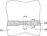
Fig. 3 A~3F is the manufacturing process profile of first embodiment of the invention dot structure, and Fig. 4 A~4D is the manufacturing process top view of first embodiment of the invention dot structure.Please refer to Fig. 3 A and Fig. 4 A, one pixel structure process method of the present invention comprises the following steps: at first, and a substrate 202 is provided.Then, form a first grid 204 and one scan line 206 on substrate 202, and first grid 204 electrically connects with scan line 206.Certainly, have in the affiliated technical field and know that usually the knowledgeable should know that first grid 204 also can be that the part of scan line 206 stretches out and forms, the shape of the first grid 204 of Fig. 4 A is only in order to explanation, limitation painstakingly.
In detail, can to see through with scan line 206 be that physical vaporous deposition (PVD) deposit metallic material is on substrate 202 for example for first grid 204.Then, this metal material is carried out patterning, can finish the making of first grid 204 and scan line 206 by one light shield processing procedure.The optional use-case of above-mentioned metal material is low resistance material such as aluminium, gold, copper, molybdenum, chromium and combined alloy thereof in this way.
Then, form an insulating barrier 208, to cover first grid 204, scan line 206 and substrate 202 partly.The material of insulating barrier 208 for example is silicon nitride (SiN
x) or silica (SiO
x) wait material.Here be noted that Fig. 4 A has omitted illustrating of insulating barrier 208 for graphic simple and clear, and insulating barrier 208 can be known and sees among Fig. 3 A.
Please refer to Fig. 3 B and 4B afterwards, form a channel architecture layer 210 on the insulating barrier 208 of first grid 204 tops.Generally speaking, can to see through be that chemical vapour deposition technique (CVD) deposition of amorphous silicon (amorphous silicon) material is on substrate 202 for example for above-mentioned channel architecture layer 210.Then, amorphous silicon (amorphoussilicon) material that is deposited on the substrate 202 is carried out patterning, can finish the making of channel architecture layer 210 by one light shield processing procedure.Here be noted that channel architecture layer 210 of the present invention also can be a sandwich construction, will be specified among second embodiment after a while except forming the channel architecture layer 210 with one deck amorphous silicon (amorphous silicon) material.
Please refer to Fig. 3 C afterwards, descend in order to make the contact impedance between semi-conducting material and the metal material.In one embodiment, on channel architecture layer 210 and partial insulating layer 208, form a doped semiconductor material layer S and a metal level M in regular turn.Above-mentioned doped semiconductor material layer S can form by chemical vapour deposition technique (CVD), and metal level M can form by the long-pending method (PVD) in physical vapor Shen.
Please refer to Fig. 3 D and Fig. 4 C then, patterned metal layer M and doped semiconductor material layer S, so that the metal level M of part forms an one source pole 214 and a drain electrode 216, the metal level M of part forms a data wire 212.Wherein, source electrode 214 electrically connects with data wire 212.On the other hand, after doped semiconductor material layer S is patterned, to I haven't seen you for ages between the sidewall of source electrode 214 and channel architecture layer 210 and drain 216 and another sidewall of channel architecture layer 210 between, form an ohmic contact layer 211.So far above-mentioned, first grid 204 of the present invention, insulating barrier 208, channel architecture layer 210, ohmic contact layer 211, source electrode 214 can tentatively constitute thin-film transistor T of the present invention with drain electrode 216.
Specifically, source electrode 214 shown in Fig. 3 D and the two side of drain electrode 216 meetings along channel architecture layer 210, and extend upward with the direction away from substrate 202.Thus, source electrode 214 of the present invention, drain electrode 216 can significantly reduce with the area that first grid 204 overlaps (overlap).As shown in Figure 1, known source electrode 112, drain electrode 114 are to extend with the direction of parallel substrate 102.This not only can't effectively reduce the occupied area of known thin-film transistor 100, and the gate-to-drain parasitic capacitance also can't effectively reduce.In comparison, the gate-to-drain parasitic capacitance that the gate-to-drain parasitic capacitance (Cgd) of thin-film transistor T of the present invention can more known thin-film transistor 100 significantly reduces.Therefore, thin-film transistor T of the present invention can have good component characteristic.In addition, the occupied area of whole thin-film transistor T also can effectively reduce.
Please refer to Fig. 3 E afterwards, form a protective layer 218, at least cover data line 212, source electrode 214, drain electrode 216, partial insulating layer 208 and channel architecture layer 210 partly.Wherein, protective layer 218 has one first contact window C1, to expose the drain electrode 216 of part.In addition, has one second contact window C2 in insulating barrier 208 and the protective layer 218, to expose the scan line 206 of part.
Then please refer to Fig. 3 F and Fig. 4 D, form a pixel electrode 220 on protective layer 218.Pixel electrode 220 sees through the first contact window C1 of protective layer 218 and electrically connects with drain electrode 216.So far above-mentioned, dot structure P of the present invention completes.Because thin-film transistor T of the present invention can effectively reduce its occupied area, so the aperture opening ratio of dot structure P of the present invention (aperture ratio) can effectively promote.
It should be noted that when forming pixel electrode 220, also optionally form a second grid 222 in the lump.The material of second grid 222 is identical with the material of pixel electrode 220, and it for example is indium tin oxide (ITO), indium-zinc oxide (IZO) or aluminium zinc oxide (AZO).Second grid 222 is positioned on the protective layer 218 of channel architecture layer 210 top at least.In addition, the second grid 222 of part extends to scan line 206 tops, and sees through the second contact window C2 in insulating barrier 208 and the protective layer 218, and electrically connects with scan line 206.
Above-mentioned first grid 204, insulating barrier 208, channel architecture layer 210, ohmic contact layer 211, source electrode 214, drain electrode 216 and second grid 222 can constitute the thin-film transistor T of bigrid kenel.When thin-film transistor T is unlocked, first grid 204 can with the side coupling of channel architecture layer 210, second grid 222 can with the opposite side coupling of channel architecture layer 210, forming two passages respectively, and then make thin-film transistor T that preferable ducting capacity can be arranged.
Second embodiment
Second embodiment and first embodiment are similar, and both main difference parts are the making of channel architecture layer.Fig. 5 A~5G is the manufacturing process profile of second embodiment of the invention dot structure, and Fig. 6 A~6D is the manufacturing process top view of second embodiment of the invention dot structure.Please refer to Fig. 5 A and Fig. 6 A, at first, provide a substrate 202.Then, form a first grid 204 and one scan line 206 on substrate 202, and first grid 204 electrically connects with scan line 206.Above-mentioned formation first grid 204 is similar with the mode and first embodiment of scan line 206, does not add to give unnecessary details in this.Then, form an insulating barrier 208, to cover first grid 204, scan line 206 and substrate 202 partly.For graphic simple and clear, Fig. 6 A has omitted illustrating of insulating barrier 208, and insulating barrier 208 can be known and sees among Fig. 5 A.
Please refer to Fig. 5 B afterwards, on insulating barrier 208, form semiconductor material layer 210a, a spacer material layer 210b and semiconductor material layer 210c in regular turn.The material of barrier layer 210b for example is insulating material, contain the insulating material of P type admixture (dopant) or contain the amorphous silicon of P type admixture.
Then please refer to Fig. 5 C and 6B, patterned semiconductor material layer 210a, spacer material layer 210b and semiconductor material layer 210c are to form a channel architecture layer 210 ' on the insulating barrier 208 of grid top.Specifically, channel architecture layer 210 ' comprises one first semiconductor layer 210a ', a barrier layer 210b ' and one second semiconductor layer 210c '.Wherein, the first semiconductor layer 210a ' is positioned on the insulating barrier 208, and barrier layer 210b ' is positioned between the first semiconductor layer 210a ' and the second semiconductor layer 210c '.
Please refer to Fig. 5 D then, descend in order to make the contact impedance between semi-conducting material and the metal material.In one embodiment, on the insulating barrier 208 of channel architecture layer 210 ' and part, form a doped semiconductor material layer S and a metal level M in regular turn.The method and first embodiment that form doped semiconductor material layer S and metal level M are similar, do not add to give unnecessary details in this.
Then please refer to Fig. 5 E and Fig. 6 C, patterned metal layer M and doped semiconductor material layer S, so that the metal level M of part forms an one source pole 214 and a drain electrode 216, and the metal level M of part forms a data wire 212.Wherein, source electrode 214 electrically connects with data wire 212.On the other hand, after doped semiconductor material layer S is patterned, can between the sidewall of source electrode 214 and channel architecture layer 210 ' and drain 216 and another sidewall of channel architecture layer 210 ' between, form an ohmic contact layer 211.So far above-mentioned, first grid 204 of the present invention, insulating barrier 208, channel architecture layer 210 ', ohmic contact layer 211, source electrode 214 can constitute thin-film transistor T of the present invention with drain electrode 216 ".
Thin-film transistor T shown in Fig. 5 E " have the advantage of the first embodiment thin-film transistor T equally.Specifically, as thin-film transistor T " bestowed reverse bias and when closing, be positioned at barrier layer 210b ' in the middle of the channel architecture layer 210 ' and can effectively suppress situation as known leakage current L shown in Figure 2.In order to improve the effect that suppresses leakage current L, barrier layer 210b ' for example is the insulating material of P type admixture (dopant) or the amorphous silicon that contains P type admixture, with effective leakage current that neutralizes and produced in channel architecture layer 210 '.Therefore, thin-film transistor T of the present invention " can have good component characteristic.
Then please refer to Fig. 5 F, form a protective layer 218, cover source electrode 214, drain electrode 216, data wire 212 and partial insulating layer 208 at least.Wherein, protective layer 218 has one first contact window C1, to expose drain electrode 216.In addition, has one second contact window C2 in insulating barrier 208 and the protective layer 218, to expose the scan line 206 of part.
Please refer to Fig. 5 G and Fig. 6 D afterwards, form a pixel electrode 220 on protective layer 218.Wherein, pixel electrode 220 sees through the first contact window C1 in the protective layer 218 and electrically connects with drain electrode 216.So far above-mentioned, dot structure P ' of the present invention completes.
It should be noted that when forming pixel electrode 220, also optionally form a second grid 222 in the lump.The material of second grid 222 is identical with the material of pixel electrode 220, and it for example is indium tin oxide, indium-zinc oxide or aluminium zinc oxide.This second grid 222 is positioned on the protective layer 218 of channel architecture layer 210 ' top.The second grid 222 of part extends to scan line 206 tops, and electrically connects with scan line 206 through the second contact window C2 in protective layer 218 and the insulating barrier 208.
What will specify here is that first grid 204, insulating barrier 208, channel architecture layer 210 ', ohmic contact layer 211, source electrode 214, drain electrode 216 and second grid 222 can constitute the thin-film transistor T ' of bigrid kenel ".As thin-film transistor T ' " when being unlocked, first grid 204 can be coupled with the first semiconductor layer 210a ', and second grid 222 meetings and the second semiconductor layer 210c ' coupling are so that thin-film transistor T ' can have preferable ducting capacity.Specifically, barrier layer 210b ' can effectively avoid electric field between the first grid 204 and the first semiconductor layer 210a ' and the electric field between the second grid 222 and the second semiconductor layer 210c ' to interact, and then can make thin-film transistor T ' " bring into play its maximum benefit.
In sum, method of manufacturing thin film transistor of the present invention is formed at source electrode and drain electrode on the two side of channel architecture layer, and makes source electrode and drain to extend away from the direction of substrate.Therefore, the overlapping area of source electrode, drain electrode and first grid can effectively reduce, and then effectively suppresses the generation of gate-to-drain electric capacity (Cgd) in the thin-film transistor.The shared area of thin-film transistor of the present invention also can effectively dwindle.In addition, can form two passages in the channel architecture layer of the present invention, thereby preferable ducting capacity can be arranged, and can effectively avoid the generation of leakage current by barrier layer.In addition, the electric field that barrier layer can effectively be avoided forming two passages produces bad interference each other, thereby can make thin-film transistor of the present invention can bring into play its greatest benefit.One pixel structure process method of the present invention can be applied to thin-film transistor of the present invention in the dot structure, thereby can make dot structure of the present invention have high aperture opening ratio.
Though the present invention with preferred embodiment openly as above; right its is not in order to limit the present invention; have in the technical field under any and know the knowledgeable usually; without departing from the spirit and scope of the present invention; when can doing a little change and retouching, so protection scope of the present invention is as the criterion when looking claims person of defining.
Claims (19)
1. a method of manufacturing thin film transistor is characterized in that, comprising:
One substrate is provided;
Form a first grid on this substrate;
Form an insulating barrier, to cover this first grid;
Form a channel architecture layer on this insulating barrier;
Form a metal level, to cover this channel architecture layer and this insulating barrier partly;
This metal level of patterning also keeps this metal level on this channel architecture layer two side, to form an one source pole and a drain electrode respectively; And
Form a protective layer, cover this source electrode, this drain electrode.
2. method of manufacturing thin film transistor as claimed in claim 1 is characterized in that, also comprises forming a second grid on this protective layer of this channel architecture layer top.
3. method of manufacturing thin film transistor as claimed in claim 2 is characterized in that, the material of this second grid comprises indium tin oxide, indium-zinc oxide or aluminium zinc oxide.
4. method of manufacturing thin film transistor as claimed in claim 1, it is characterized in that, this channel architecture layer comprises one first semiconductor layer, a barrier layer and one second semiconductor layer, this first semiconductor layer is positioned on this insulating barrier, and this barrier layer is between this first semiconductor layer and this second semiconductor layer.
5. method of manufacturing thin film transistor as claimed in claim 4 is characterized in that, the material of this barrier layer comprises insulating material or comprises insulating material and P type admixture or comprise amorphous silicon and P type admixture.
6. method of manufacturing thin film transistor as claimed in claim 1 is characterized in that, also is included between the sidewall of this source electrode and this channel architecture layer and between another sidewall of this drain electrode and this channel architecture layer, forms an ohmic contact layer.
7. a thin-film transistor is suitable for being disposed on the substrate, it is characterized in that, this thin-film transistor comprises:
One first grid is disposed on this substrate;
One insulating barrier covers this first grid;
One channel architecture layer is disposed on this insulating barrier;
An one source pole and a drain electrode are disposed at respectively on the two side of this channel architecture layer;
One protective layer covers this source electrode, this drain electrode and this insulating barrier partly at least.
8. thin-film transistor as claimed in claim 7 is characterized in that, this source electrode and this drain electrode are to extend away from the direction of this substrate.
9. thin-film transistor as claimed in claim 7 is characterized in that, also comprises an ohmic contact layer, is disposed between the sidewall of this source electrode and this channel architecture layer, and is disposed between another sidewall of this drain electrode and this channel architecture layer.
10. thin-film transistor as claimed in claim 7 is characterized in that, also comprises a second grid, is disposed on this protective layer of this channel architecture layer top.
11. thin-film transistor as claimed in claim 7, it is characterized in that, this channel architecture layer comprises one first semiconductor layer, a barrier layer and one second semiconductor layer, and this first semiconductor layer is positioned on this insulating barrier, and this barrier layer is between this first semiconductor layer and this second semiconductor layer.
12. an one pixel structure process method is characterized in that, comprising:
One substrate is provided;
Form a first grid and one scan line on this substrate, and this first grid and the electric connection of this scan line;
Form an insulating barrier, to cover this first grid, this scan line and this substrate partly;
Form a channel architecture layer on this insulating barrier;
Form a metal level, to cover this channel architecture layer;
This metal level of patterning, to form a data wire and to keep this metal level on this channel architecture layer two side at least, to form one source pole and a drain electrode respectively, wherein this source electrode and this data wire electric connection;
Form a protective layer, cover this source electrode, this drain electrode, this data wire and this insulating barrier partly at least; And
Form a pixel electrode on this protective layer, wherein this pixel electrode sees through one first contact window in this protective layer and electrically connects with this drain electrode.
13. one pixel structure process method as claimed in claim 12; it is characterized in that; also comprise when forming this pixel electrode and form a second grid in the lump; this second grid is positioned on this protective layer of this channel architecture layer top at least and part extends to this scan line top; and through one second contact window in this protective layer and this insulating barrier, and electrically connect with this scan line.
14. one pixel structure process method as claimed in claim 13, it is characterized in that, this channel architecture layer comprises one first semiconductor layer, a barrier layer and one second semiconductor layer, this first semiconductor layer is positioned on this insulating barrier, and this barrier layer is between this first semiconductor layer and this second semiconductor layer.
15. one pixel structure process method as claimed in claim 13 is characterized in that, also is included between the sidewall of this source electrode and this channel architecture layer and between another sidewall of this drain electrode and this channel architecture layer, forms an ohmic contact layer.
16. a dot structure is suitable for being disposed on the substrate, it is characterized in that, this dot structure comprises:
One first grid is disposed on this substrate;
The one scan line is disposed on this substrate and electrically connects with this first grid;
One insulating barrier covers this first grid, this scan line and this substrate partly;
One channel architecture layer is disposed on this insulating barrier;
One data wire is disposed on this insulating barrier;
An one source pole and a drain electrode are disposed at respectively on the two side of this channel architecture layer;
One protective layer covers this source electrode, this drain electrode, this data wire and this insulating barrier partly at least; And
One pixel electrode is disposed on this protective layer, and wherein this pixel electrode sees through one first contact window in this protective layer and electrically connects with this drain electrode.
17. dot structure as claimed in claim 16 is characterized in that, this source electrode and this drain electrode are to extend away from the direction of this substrate.
18. dot structure as claimed in claim 16; it is characterized in that; also comprise a second grid; be disposed on this protective layer of this channel architecture layer top and part extends to this scan line top; and through one second contact window in this protective layer and this insulating barrier, and electrically connect with this scan line.
19. dot structure as claimed in claim 16, it is characterized in that, this channel architecture layer comprises one first semiconductor layer, a barrier layer and one second semiconductor layer, and this first semiconductor layer is positioned on this insulating barrier, and this barrier layer is between this first semiconductor layer and this second semiconductor layer.
Priority Applications (1)
| Application Number | Priority Date | Filing Date | Title |
|---|---|---|---|
| CN200810167061A CN101728265A (en) | 2008-10-10 | 2008-10-10 | Thin film transistor, pixel structure and manufacturing method thereof |
Applications Claiming Priority (1)
| Application Number | Priority Date | Filing Date | Title |
|---|---|---|---|
| CN200810167061A CN101728265A (en) | 2008-10-10 | 2008-10-10 | Thin film transistor, pixel structure and manufacturing method thereof |
Publications (1)
| Publication Number | Publication Date |
|---|---|
| CN101728265A true CN101728265A (en) | 2010-06-09 |
Family
ID=42448925
Family Applications (1)
| Application Number | Title | Priority Date | Filing Date |
|---|---|---|---|
| CN200810167061A Pending CN101728265A (en) | 2008-10-10 | 2008-10-10 | Thin film transistor, pixel structure and manufacturing method thereof |
Country Status (1)
| Country | Link |
|---|---|
| CN (1) | CN101728265A (en) |
Cited By (2)
| Publication number | Priority date | Publication date | Assignee | Title |
|---|---|---|---|---|
| CN104635388A (en) * | 2013-11-08 | 2015-05-20 | 群创光电股份有限公司 | Display panel and display device including the display panel |
| CN106125432A (en) * | 2016-08-29 | 2016-11-16 | 武汉华星光电技术有限公司 | Display and display floater thereof |
-
2008
- 2008-10-10 CN CN200810167061A patent/CN101728265A/en active Pending
Cited By (5)
| Publication number | Priority date | Publication date | Assignee | Title |
|---|---|---|---|---|
| CN104635388A (en) * | 2013-11-08 | 2015-05-20 | 群创光电股份有限公司 | Display panel and display device including the display panel |
| CN104635388B (en) * | 2013-11-08 | 2018-04-03 | 群创光电股份有限公司 | Display panel and display device comprising same |
| CN106125432A (en) * | 2016-08-29 | 2016-11-16 | 武汉华星光电技术有限公司 | Display and display floater thereof |
| WO2018040468A1 (en) * | 2016-08-29 | 2018-03-08 | 武汉华星光电技术有限公司 | Display and display panel thereof |
| US10216058B2 (en) | 2016-08-29 | 2019-02-26 | Wuhan China Star Optoelectronics Technology Co., Ltd | Display devices and the display panels thereof |
Similar Documents
| Publication | Publication Date | Title |
|---|---|---|
| US20100044708A1 (en) | Thin film transistor, pixel structure and fabrication methods thereof | |
| US9455333B2 (en) | Thin film transistor array panel | |
| US10451946B2 (en) | Semiconductor device, liquid crystal display device, and semiconductor device manufacturing method | |
| US9236405B2 (en) | Array substrate, manufacturing method and the display device thereof | |
| US7095460B2 (en) | Thin film transistor array substrate using low dielectric insulating layer and method of fabricating the same | |
| US9257563B2 (en) | Thin film transistor array panel and method of manufacturing the same | |
| KR101325053B1 (en) | Thin film transistor substrate and manufacturing method thereof | |
| CN103219389B (en) | A kind of thin-film transistor and preparation method thereof, array base palte and display unit | |
| US8835216B2 (en) | Thin-film transistor, method of fabricating the thin-film transistor, and display substrate using the thin-film transistor | |
| US20100051933A1 (en) | Thin film transistor array substrate and method of fabricating the same | |
| KR102089244B1 (en) | Double gate type thin film transistor and organic light emitting diode display device including the same | |
| CN102315254B (en) | The liquid crystal display of thin film transistor base plate and this thin film transistor base plate of employing | |
| US20100155721A1 (en) | Thin film transistor array substrate and method of fabricating the same | |
| US20150187948A1 (en) | Semiconductor device and method for producing same | |
| CN101697054B (en) | A Pixel Design with Increased Aperture Ratio for Liquid Crystal Displays | |
| KR20090079686A (en) | Thin film transistor substrate and manufacturing method thereof | |
| US8629949B2 (en) | Liquid crystal display and method of forming the same | |
| US11791414B2 (en) | TFT device, manufacturing method thereof, and array substrate | |
| CN109273365A (en) | Preparation method of thin film transistor, thin film transistor and display panel | |
| CN106483726A (en) | Thin-film transistor array base-plate and preparation method and display panels | |
| US8748892B2 (en) | Thin film transistor and method for fabricating the same | |
| EP2261733B1 (en) | Pixel designs for improving the aperture ratio of a liquid crystal display | |
| US8912027B2 (en) | Display device and method of manufacturing the same | |
| CN101728265A (en) | Thin film transistor, pixel structure and manufacturing method thereof | |
| CN101533805A (en) | Pixel structure and manufacturing method thereof |
Legal Events
| Date | Code | Title | Description |
|---|---|---|---|
| C06 | Publication | ||
| PB01 | Publication | ||
| C10 | Entry into substantive examination | ||
| SE01 | Entry into force of request for substantive examination | ||
| C02 | Deemed withdrawal of patent application after publication (patent law 2001) | ||
| WD01 | Invention patent application deemed withdrawn after publication |
Open date: 20100609 |