CN101615380B - Display apparatus, driving method for display apparatus and electronic apparatus - Google Patents
Display apparatus, driving method for display apparatus and electronic apparatus Download PDFInfo
- Publication number
- CN101615380B CN101615380B CN2009101503204A CN200910150320A CN101615380B CN 101615380 B CN101615380 B CN 101615380B CN 2009101503204 A CN2009101503204 A CN 2009101503204A CN 200910150320 A CN200910150320 A CN 200910150320A CN 101615380 B CN101615380 B CN 101615380B
- Authority
- CN
- China
- Prior art keywords
- transistor
- period
- mobility correction
- display panel
- organic
- Prior art date
- Legal status (The legal status is an assumption and is not a legal conclusion. Google has not performed a legal analysis and makes no representation as to the accuracy of the status listed.)
- Expired - Fee Related
Links
Images


Classifications
-
- G—PHYSICS
- G09—EDUCATION; CRYPTOGRAPHY; DISPLAY; ADVERTISING; SEALS
- G09G—ARRANGEMENTS OR CIRCUITS FOR CONTROL OF INDICATING DEVICES USING STATIC MEANS TO PRESENT VARIABLE INFORMATION
- G09G3/00—Control arrangements or circuits, of interest only in connection with visual indicators other than cathode-ray tubes
- G09G3/20—Control arrangements or circuits, of interest only in connection with visual indicators other than cathode-ray tubes for presentation of an assembly of a number of characters, e.g. a page, by composing the assembly by combination of individual elements arranged in a matrix no fixed position being assigned to or needed to be assigned to the individual characters or partial characters
- G09G3/22—Control arrangements or circuits, of interest only in connection with visual indicators other than cathode-ray tubes for presentation of an assembly of a number of characters, e.g. a page, by composing the assembly by combination of individual elements arranged in a matrix no fixed position being assigned to or needed to be assigned to the individual characters or partial characters using controlled light sources
- G09G3/30—Control arrangements or circuits, of interest only in connection with visual indicators other than cathode-ray tubes for presentation of an assembly of a number of characters, e.g. a page, by composing the assembly by combination of individual elements arranged in a matrix no fixed position being assigned to or needed to be assigned to the individual characters or partial characters using controlled light sources using electroluminescent panels
- G09G3/32—Control arrangements or circuits, of interest only in connection with visual indicators other than cathode-ray tubes for presentation of an assembly of a number of characters, e.g. a page, by composing the assembly by combination of individual elements arranged in a matrix no fixed position being assigned to or needed to be assigned to the individual characters or partial characters using controlled light sources using electroluminescent panels semiconductive, e.g. using light-emitting diodes [LED]
- G09G3/3208—Control arrangements or circuits, of interest only in connection with visual indicators other than cathode-ray tubes for presentation of an assembly of a number of characters, e.g. a page, by composing the assembly by combination of individual elements arranged in a matrix no fixed position being assigned to or needed to be assigned to the individual characters or partial characters using controlled light sources using electroluminescent panels semiconductive, e.g. using light-emitting diodes [LED] organic, e.g. using organic light-emitting diodes [OLED]
- G09G3/3225—Control arrangements or circuits, of interest only in connection with visual indicators other than cathode-ray tubes for presentation of an assembly of a number of characters, e.g. a page, by composing the assembly by combination of individual elements arranged in a matrix no fixed position being assigned to or needed to be assigned to the individual characters or partial characters using controlled light sources using electroluminescent panels semiconductive, e.g. using light-emitting diodes [LED] organic, e.g. using organic light-emitting diodes [OLED] using an active matrix
- G09G3/3233—Control arrangements or circuits, of interest only in connection with visual indicators other than cathode-ray tubes for presentation of an assembly of a number of characters, e.g. a page, by composing the assembly by combination of individual elements arranged in a matrix no fixed position being assigned to or needed to be assigned to the individual characters or partial characters using controlled light sources using electroluminescent panels semiconductive, e.g. using light-emitting diodes [LED] organic, e.g. using organic light-emitting diodes [OLED] using an active matrix with pixel circuitry controlling the current through the light-emitting element
-
- G—PHYSICS
- G09—EDUCATION; CRYPTOGRAPHY; DISPLAY; ADVERTISING; SEALS
- G09G—ARRANGEMENTS OR CIRCUITS FOR CONTROL OF INDICATING DEVICES USING STATIC MEANS TO PRESENT VARIABLE INFORMATION
- G09G2300/00—Aspects of the constitution of display devices
- G09G2300/08—Active matrix structure, i.e. with use of active elements, inclusive of non-linear two terminal elements, in the pixels together with light emitting or modulating elements
- G09G2300/0809—Several active elements per pixel in active matrix panels
- G09G2300/0819—Several active elements per pixel in active matrix panels used for counteracting undesired variations, e.g. feedback or autozeroing
-
- G—PHYSICS
- G09—EDUCATION; CRYPTOGRAPHY; DISPLAY; ADVERTISING; SEALS
- G09G—ARRANGEMENTS OR CIRCUITS FOR CONTROL OF INDICATING DEVICES USING STATIC MEANS TO PRESENT VARIABLE INFORMATION
- G09G2300/00—Aspects of the constitution of display devices
- G09G2300/08—Active matrix structure, i.e. with use of active elements, inclusive of non-linear two terminal elements, in the pixels together with light emitting or modulating elements
- G09G2300/0809—Several active elements per pixel in active matrix panels
- G09G2300/0823—Several active elements per pixel in active matrix panels used to establish symmetry in driving, e.g. with polarity inversion
-
- G—PHYSICS
- G09—EDUCATION; CRYPTOGRAPHY; DISPLAY; ADVERTISING; SEALS
- G09G—ARRANGEMENTS OR CIRCUITS FOR CONTROL OF INDICATING DEVICES USING STATIC MEANS TO PRESENT VARIABLE INFORMATION
- G09G2300/00—Aspects of the constitution of display devices
- G09G2300/08—Active matrix structure, i.e. with use of active elements, inclusive of non-linear two terminal elements, in the pixels together with light emitting or modulating elements
- G09G2300/0809—Several active elements per pixel in active matrix panels
- G09G2300/0842—Several active elements per pixel in active matrix panels forming a memory circuit, e.g. a dynamic memory with one capacitor
- G09G2300/0852—Several active elements per pixel in active matrix panels forming a memory circuit, e.g. a dynamic memory with one capacitor being a dynamic memory with more than one capacitor
-
- G—PHYSICS
- G09—EDUCATION; CRYPTOGRAPHY; DISPLAY; ADVERTISING; SEALS
- G09G—ARRANGEMENTS OR CIRCUITS FOR CONTROL OF INDICATING DEVICES USING STATIC MEANS TO PRESENT VARIABLE INFORMATION
- G09G2300/00—Aspects of the constitution of display devices
- G09G2300/08—Active matrix structure, i.e. with use of active elements, inclusive of non-linear two terminal elements, in the pixels together with light emitting or modulating elements
- G09G2300/0809—Several active elements per pixel in active matrix panels
- G09G2300/0842—Several active elements per pixel in active matrix panels forming a memory circuit, e.g. a dynamic memory with one capacitor
- G09G2300/0861—Several active elements per pixel in active matrix panels forming a memory circuit, e.g. a dynamic memory with one capacitor with additional control of the display period without amending the charge stored in a pixel memory, e.g. by means of additional select electrodes
- G09G2300/0866—Several active elements per pixel in active matrix panels forming a memory circuit, e.g. a dynamic memory with one capacitor with additional control of the display period without amending the charge stored in a pixel memory, e.g. by means of additional select electrodes by means of changes in the pixel supply voltage
-
- G—PHYSICS
- G09—EDUCATION; CRYPTOGRAPHY; DISPLAY; ADVERTISING; SEALS
- G09G—ARRANGEMENTS OR CIRCUITS FOR CONTROL OF INDICATING DEVICES USING STATIC MEANS TO PRESENT VARIABLE INFORMATION
- G09G2320/00—Control of display operating conditions
- G09G2320/04—Maintaining the quality of display appearance
- G09G2320/041—Temperature compensation
-
- G—PHYSICS
- G09—EDUCATION; CRYPTOGRAPHY; DISPLAY; ADVERTISING; SEALS
- G09G—ARRANGEMENTS OR CIRCUITS FOR CONTROL OF INDICATING DEVICES USING STATIC MEANS TO PRESENT VARIABLE INFORMATION
- G09G2320/00—Control of display operating conditions
- G09G2320/04—Maintaining the quality of display appearance
- G09G2320/043—Preventing or counteracting the effects of ageing
- G09G2320/045—Compensation of drifts in the characteristics of light emitting or modulating elements
Landscapes
- Engineering & Computer Science (AREA)
- Physics & Mathematics (AREA)
- Computer Hardware Design (AREA)
- General Physics & Mathematics (AREA)
- Theoretical Computer Science (AREA)
- Control Of El Displays (AREA)
- Control Of Indicators Other Than Cathode Ray Tubes (AREA)
- Electroluminescent Light Sources (AREA)
Abstract
Description
相关申请的交叉引用 Cross References to Related Applications
本申请包含与2008年6月23日在日本专利局提交的日本优先权专利申请JP2008-162738中所公开的主题有关的主题,其全部内容通过引用被合并于此。 The present application contains subject matter related to that disclosed in Japanese Priority Patent Application JP2008-162738 filed in the Japan Patent Office on Jun. 23, 2008, the entire content of which is hereby incorporated by reference. the
技术领域 technical field
本发明涉及一种显示装置、一种用于显示装置的驱动方法以及一种电子装置,更具体地,涉及一种在其中以矩阵形式二维地布置了多个像素的扁平类型或者平板类型的显示装置、一种用于该显示装置的驱动方法、以及一种并入了所述显示装置的电子装置。 The present invention relates to a display device, a driving method for the display device, and an electronic device, and more particularly, to a flat type or panel type in which a plurality of pixels are two-dimensionally arranged in a matrix. A display device, a driving method for the display device, and an electronic device incorporating the display device. the
背景技术 Background technique
近些年来,在显示图像的显示装置领域,很快普及了一种在其中以矩阵(即,以行和列)布置多个像素和像素电路的扁平类型的显示装置。这种扁平类型的显示装置中的一种显示装置使用电流驱动型的电光(electro-optical)元件作为像素的发光元件,所述电光元件的发光亮度响应于流过该元件的电流值而变化。作为电流驱动型的电光元件的有机EL(电致发光(ElectroLuminescence)元件是已知的,有机EL元件利用了当向有机薄膜施加电场时有机薄膜发光的现象。 In recent years, in the field of display devices that display images, a flat type display device in which a plurality of pixels and pixel circuits are arranged in a matrix (ie, in rows and columns) has rapidly spread. One of such flat type display devices uses, as a light emitting element of a pixel, a current-driven electro-optical element whose light emission luminance varies in response to the value of a current flowing through the element. An organic EL (ElectroLuminescence) element is known as a current-driven electro-optical element, and the organic EL element utilizes a phenomenon in which an organic thin film emits light when an electric field is applied to the organic thin film.
使用有机EL元件作为像素的电光元件的有机EL显示装置具有以下的特点。具体地,由于有机EL元件能够被等于或者低于10V的施加电压驱动,因此其具有低功耗的特点。由于有机EL元件是自发光元件,因此相比于通过使用每个像素的液晶控制来自光源的光的强度来显示图像的液晶显示装置而言,有机EL元件显示了高能见度的图像。另外,由于有机EL元件不需要诸如背光之类的照明部件,其有利于减少有机EL显示装置的重量和厚度。此外,由于响应速度近似高达几个微妙,因此不会在动态画面显示上出现后像(after-image)。 An organic EL display device using an organic EL element as an electro-optic element of a pixel has the following features. Specifically, since the organic EL element can be driven by an applied voltage equal to or lower than 10V, it has a feature of low power consumption. Since the organic EL element is a self-luminous element, the organic EL element displays an image with high visibility compared to a liquid crystal display device that displays an image by controlling the intensity of light from a light source using a liquid crystal of each pixel. In addition, since the organic EL element does not require lighting components such as a backlight, it contributes to reducing the weight and thickness of the organic EL display device. In addition, since the response speed is approximately up to several microseconds, there will be no after-image on the dynamic picture display. the
有机EL显示装置能够采取简单的或者无源矩阵类型或者有源矩阵类型作为其驱动方法,类似于液晶显示装置。然而,尽管简单的矩阵类型的显示装置在结构上简单,但是其问题在于很难将该显示装置实现为大尺寸的高清晰度的显示装置,这是因为每个电光元件的发光时段随着扫描线的数量(即,像素的数量)的增加而减少。 An organic EL display device can adopt a simple or passive matrix type or an active matrix type as its driving method, similarly to a liquid crystal display device. However, although a simple matrix type display device is structurally simple, it has a problem in that it is difficult to realize the display device as a large-sized high-definition display device because the light emission period of each electro-optical element varies with the scanning The number of lines (ie, the number of pixels) increases and decreases. the
因此,在近些年,有源矩阵显示装置的开发一直在并且还正在蓬勃地进行,在该有源矩阵显示装置中,通过在像素中提供的有源元件来控制流过电光元件(其中,该电光元件被提供为诸如绝缘栅型场效应晶体管)的电流。通常使用薄膜晶体管(TFT)作为绝缘栅型场效应晶体管。因为电光元件在一帧的时段上持续地发光,所以有源矩阵显示装置能够被容易地实现为大尺寸并且高清晰度的显示装置。 Therefore, in recent years, the development of active-matrix display devices in which the flow through electro-optical elements (wherein, The electro-optical element is supplied with current such as an insulated gate field effect transistor. Thin film transistors (TFTs) are generally used as insulated gate type field effect transistors. Since the electro-optic element continuously emits light over a period of one frame, the active matrix display device can be easily realized as a large-sized and high-definition display device. the
附带地,通常已知有机EL元件的I-V特性,即,电流-电压特性随时间流逝而劣化(老化劣化)。在使用具体是N沟道类型的TFT作为用于通过电流驱动有机EL元件的晶体管(下文中称为驱动晶体管)的像素电路中,如果有机EL元件的I-V特性遭受到老化劣化,则驱动晶体管的栅极-源极电压Vgs变化。结果,有机EL元件的发光亮度变化。这是由于以下事实产生的:即,有机EL元件被连接到驱动晶体管的源极电极侧。 Incidentally, it is generally known that I-V characteristics of organic EL elements, that is, current-voltage characteristics deteriorate with the lapse of time (aging deterioration). In a pixel circuit using a TFT, specifically, an N-channel type as a transistor for driving an organic EL element by current (hereinafter referred to as a driving transistor), if the I-V characteristic of the organic EL element suffers from aging deterioration, the driving transistor's The gate-source voltage Vgs varies. As a result, the emission luminance of the organic EL element varies. This is due to the fact that the organic EL element is connected to the source electrode side of the drive transistor. the
对此进行更具体的描述。驱动晶体管的源极电势依赖于驱动晶体管和有机EL元件的工作点。那么,如果有机EL元件的I-V特性劣化,则由于驱动晶体管和有机EL元件的工作点变化,即使相同的电压被施加到驱动晶体管的栅极电极,驱动晶体管的源极电势也改变。相应地,驱动晶体管的源极-栅极电压Vgs变化并且流到驱动晶体管的电流的值也改变。结果,由于流到有机EL元件的电流的值也变化,有机EL元件的发光亮度变化。 Describe this more specifically. The source potential of the driving transistor depends on the operating points of the driving transistor and the organic EL element. Then, if the I-V characteristic of the organic EL element deteriorates, since the operating points of the driving transistor and the organic EL element vary, even if the same voltage is applied to the gate electrode of the driving transistor, the source potential of the driving transistor changes. Accordingly, the source-gate voltage Vgs of the driving transistor changes and the value of the current flowing to the driving transistor also changes. As a result, since the value of the current flowing to the organic EL element also changes, the light emission luminance of the organic EL element changes. the
此外,具体地在使用多晶硅TFT的像素电路中,除了有机EL元件的I-V特性的老化劣化之外,驱动晶体管的晶体管特性随着时间流逝而变化或者由于制造工艺中的离散性(dispersion)在不同的像素之间晶体管的特性不同。换言之,在各个像素之间驱动晶体管的晶体管特性离散(disperse)。所述晶体管特性可以是驱动晶体管的阈电压Vth、形成驱动晶体管的沟道的半导体薄膜的迁移率μ(这种迁移率μ在下文中简单地称为“驱动晶体管的迁移率μ)或者其他的特性。 In addition, particularly in a pixel circuit using a polysilicon TFT, in addition to the aging deterioration of the I-V characteristic of the organic EL element, the transistor characteristic of the driving transistor changes with the lapse of time or varies due to dispersion in the manufacturing process. The characteristics of the transistors differ between pixels. In other words, the transistor characteristics of the driving transistors are dispersed among the respective pixels. The transistor characteristics may be threshold voltage Vth of the driving transistor, mobility μ of a semiconductor thin film forming a channel of the driving transistor (this mobility μ is hereinafter simply referred to as “mobility μ of the driving transistor), or other characteristics. .
当驱动晶体管的晶体管特性在不同的像素之间不同时,由于这产生了流 过各像素中的驱动晶体管的电流值的离散性,因此即使相同的电压被施加到各像素中的驱动晶体管的栅极电极,在各像素中的有机EL元件的发光亮度方面也出现离散。结果,损坏了屏幕图像的一致性(uniformity)。 When the transistor characteristics of the drive transistor differ from pixel to pixel, since this produces dispersion in the value of the current flowing through the drive transistor in each pixel, even if the same voltage is applied to the gate of the drive transistor in each pixel The polar electrodes also cause variations in the light emission luminance of the organic EL element in each pixel. As a result, the uniformity of the screen image is damaged. the
因此,向像素电路提供了各种校正或者补偿功能以便保持有机EL元件的发光亮度固定,而不受有机EL元件的I-V特性的老化劣化或者驱动晶体管的晶体管特性的老化劣化的影响,例如如在日本专利特许公开第2006-133542号中所公开的。 Therefore, various correction or compensation functions are provided to the pixel circuit in order to keep the emission luminance of the organic EL element constant without being affected by the aging deterioration of the I-V characteristic of the organic EL element or the aging deterioration of the transistor characteristic of the driving transistor, for example, as in It is disclosed in Japanese Patent Laid-Open No. 2006-133542. the
校正功能可以包括对于有机EL元件的特性变化的补偿功能、针对驱动晶体管的阈电压Vth的变化的校正功能、针对驱动晶体管的迁移率μ的变化的校正功能以及其他的功能。在以下给出的描述中,针对驱动晶体管的阈电压Vth的变化的校正被称为“阈值校正”,而针对驱动晶体管的迁移率μ的校正被称为“迁移率校正”。 The correction function may include a compensation function for a characteristic change of the organic EL element, a correction function for a change in the threshold voltage Vth of the driving transistor, a correction function for a change in the mobility μ of the driving transistor, and others. In the description given below, correction for variation in the threshold voltage Vth of the driving transistor is referred to as "threshold correction", and correction for the mobility μ of the driving transistor is referred to as "mobility correction". the
当以这种方式向每个像素电路配备了各种校正功能时,有机EL元件的发光亮度能够被保持固定而不受有机EL元件的I-V特性的老化劣化或者驱动晶体管的晶体管特性的老化劣化的影响。结果,能够提高有机EL显示装置的显示质量。 When each pixel circuit is equipped with various correction functions in this way, the light emission luminance of the organic EL element can be kept constant without aging deterioration of the I-V characteristic of the organic EL element or aging deterioration of the transistor characteristic of the driving transistor. Influence. As a result, the display quality of the organic EL display device can be improved. the
通过以下描述的这种一系列电路操作来执行对于有机EL元件的特性变化的补偿功能。首先,通过写入晶体管来写入通过信号线提供的图像信号以便将该图像信号存储到在驱动晶体管的栅极和源极之间的存储电容器中。此后,写入晶体管被置于不导通的状态以将驱动晶体管的栅极电极与信号线电气断开,从而将驱动晶体管的栅极电极置于浮置状态。 The compensation function for the characteristic variation of the organic EL element is performed by such a series of circuit operations described below. First, an image signal supplied through a signal line is written through a write transistor to store the image signal into a storage capacitor between a gate and a source of a drive transistor. Thereafter, the writing transistor is placed in a non-conductive state to electrically disconnect the gate electrode of the driving transistor from the signal line, thereby placing the gate electrode of the driving transistor in a floating state. the
当驱动晶体管的栅极电极被置于浮置状态时,由于在驱动晶体管的栅极和源极之间连接了存储电容器,因此驱动晶体管的栅极电势Vg以与驱动晶体管的源极电势Vs的变化成互锁关系地(即,跟随)变化。用于以与驱动晶体管的源极电势Vs成互锁关系地变化栅极电势Vg的这种方式的操作在下文中被称为自举操作。通过该自举操作,能够使驱动晶体管的栅极-源极电压Vgs保持固定。结果,即使有机EL元件的I-V特性遭受老化劣化,有机EL元件的发光亮度也能够被保持固定。 When the gate electrode of the driving transistor is placed in a floating state, since the storage capacitor is connected between the gate and the source of the driving transistor, the gate potential Vg of the driving transistor is equal to the source potential Vs of the driving transistor Changes in interlock (ie, follow) changes in . Operation in this manner for varying the gate potential Vg in an interlocking relationship with the source potential Vs of the drive transistor is hereinafter referred to as a bootstrap operation. Through this bootstrap operation, the gate-source voltage Vgs of the driving transistor can be kept constant. As a result, even if the IV characteristic of the organic EL element suffers aging deterioration, the emission luminance of the organic EL element can be kept constant.
发明内容 Contents of the invention
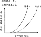
顺带提及,对于相同的信号电压,在其中以矩阵形式二维地布置了多个 像素的显示面板的发光亮度在高温状态下比在常温状态下展示了更高的级别。图25图示了显示面板的V(信号电压)-L(发光亮度)特性。显示面板的该V-L特性以此方式具有温度依赖性,这是由诸如有机EL元件之类的电光元件(元件)的温度特性引起的。 Incidentally, for the same signal voltage, the emission luminance of a display panel in which a plurality of pixels are two-dimensionally arranged in a matrix exhibits a higher level in a high-temperature state than in a normal-temperature state. FIG. 25 illustrates V (signal voltage)-L (light emission luminance) characteristics of the display panel. This V-L characteristic of the display panel has temperature dependence in this way, which is caused by the temperature characteristic of an electro-optical element (element) such as an organic EL element. the
图26图示了有机EL元件的温度特性。更具体地,图26图示了其中环境温度是常温或者室温(例如,25℃)下EL施加电压-电流密度特性的虚线和在高的环境温度状态(例如,60℃)下另一EL施加电压-电流密度特性的实线。根据该温度特性,能够看出如果环境温度变为高温状态,则由于特性曲线的上升沿变得更陡,有机EL元件的驱动电压(即,EL施加电压)从常温状态下的电压下降。 Fig. 26 illustrates temperature characteristics of an organic EL element. More specifically, FIG. 26 illustrates a dotted line of EL application voltage-current density characteristics in which the ambient temperature is normal temperature or room temperature (for example, 25° C.) and another EL application in a state of high ambient temperature (for example, 60° C.). Solid line of the voltage-current density characteristic. From this temperature characteristic, it can be seen that when the ambient temperature becomes high, the rising edge of the characteristic curve becomes steeper, and the driving voltage (ie, EL applied voltage) of the organic EL element drops from the voltage at normal temperature. the
流到有机EL元件的电流(即,流过驱动晶体管的电流,或者换言之,驱动晶体管的漏极-源极电流Ids)由以下表达式(10)表示 The current flowing to the organic EL element (that is, the current flowing through the driving transistor, or in other words, the drain-source current Ids of the driving transistor) is expressed by the following expression (10)
Ids=kμ(Vgs-(1-Gb)×ΔVs)2...(10) Ids=kμ(Vgs-(1-Gb)×ΔVs) 2 ... (10)
其中Vgs是驱动晶体管的栅极-源极电压,并且ΔVs是驱动晶体管的源极电压Vs的变化量。常数k是(1/2)(W/L)Cox,其中W是驱动晶体管的沟道宽度,L是沟道长度,Cox是每单位面积的栅极电容。 where Vgs is the gate-source voltage of the driving transistor, and ΔVs is the amount of change in the source voltage Vs of the driving transistor. The constant k is (1/2)(W/L)Cox, where W is the channel width of the drive transistor, L is the channel length, and Cox is the gate capacitance per unit area. the
此外,Gb表示自举增益。自举增益Gb是在上述自举操作中驱动晶体管的栅极电势Vg的变化量ΔVg与其源极电势Vs的变化量ΔVs的比率,并且被表示为ΔVg/ΔVs。该自举增益Gb取决于存储电容器的电容值、由驱动晶体管的栅极提供的寄生电容的电容值等等。 In addition, Gb represents a bootstrap gain. The bootstrap gain Gb is the ratio of the variation ΔVg of the gate potential Vg of the driving transistor to the variation ΔVs of the source potential Vs of the drive transistor in the above-described bootstrap operation, and is expressed as ΔVg/ΔVs. This bootstrap gain Gb depends on the capacitance value of the storage capacitor, the capacitance value of the parasitic capacitance provided by the gate of the drive transistor, and the like. the
如果显示面板的温度上升并且用于有机EL元件的驱动电压下降,则驱动晶体管的源极电势Vs的变化量ΔVs减少。相应地,由于流过驱动晶体管的电流Ids增加(如能够从上文中给出的表达式(10)中清楚地看出的),流过有机EL元件的电流也增加并且发光亮度增加。简言之,如果温度从常温变高,则在相同的驱动电压下有机EL元件的亮度变得非常高。 If the temperature of the display panel rises and the driving voltage for the organic EL element falls, the variation ΔVs of the source potential Vs of the driving transistor decreases. Accordingly, as the current Ids flowing through the drive transistor increases (as can be clearly seen from the expression (10) given above), the current flowing through the organic EL element also increases and the luminance of light emission increases. In short, if the temperature becomes higher from ordinary temperature, the luminance of the organic EL element becomes very high at the same driving voltage. the
以这种方式,有机EL元件具有以下问题:由于有机EL元件具有温度特性,则如果面板温度由于环境温度等等的上升而上升,则流到有机EL元件的电流增加,并且作为结果,显示面板的发光亮度变得比其在常温状态下的发光亮度更高。相反,如果面板温度下降,则由于流到有机EL元件的电流减少,显示面板的发光亮度变得比其在常温状态下的发光亮度低。 In this way, the organic EL element has a problem that since the organic EL element has temperature characteristics, if the panel temperature rises due to an increase in ambient temperature or the like, the current flowing to the organic EL element increases, and as a result, the display panel The luminance of luminescence becomes higher than that at normal temperature. Conversely, if the panel temperature drops, the light emission luminance of the display panel becomes lower than that in a normal temperature state because the current flowing to the organic EL element decreases. the
因此,期望提供一种显示装置、一种用于该显示装置的合适的驱动方法 以及一种合并了该显示装置的电子装置,在该显示装置中,能够将显示面板的发光亮度保持固定而不受该显示面板的温度变化的影响。 Therefore, it is desirable to provide a display device, a suitable driving method for the display device, and an electronic device incorporating the display device, in which the luminous brightness of the display panel can be kept constant without affected by temperature changes of the display panel. the
根据本发明的一个实施例,其中提供了一种显示装置,其包括:显示面板,在其上具有以矩阵形式布置的多个像素;温度检测部件,被配置为检测显示面板的温度;以及控制部件,被配置为基于由温度检测部件的检测结果来控制迁移率校正处理的时段;其中每个像素包括:电光元件、用于写入图像信号的写入晶体管、用于响应由写入晶体管写入的图像信号而驱动该电光元件的驱动晶体管、以及在驱动晶体管的栅极电极和源极电极之间连接的用于存储由写入晶体管写入的图像信号的存储电容器;每个像素执行迁移率校正处理,该迁移率校正处理用于利用从流到驱动晶体管的电流确定的校正量来对驱动晶体管的栅极和源极之间的电势差施加负反馈。 According to an embodiment of the present invention, there is provided a display device, which includes: a display panel with a plurality of pixels arranged in a matrix; a temperature detection component configured to detect the temperature of the display panel; and a control a part configured to control a period of mobility correction processing based on a detection result by the temperature detection part; wherein each pixel includes: an electro-optical element, a writing transistor for writing an image signal, a writing transistor for responding to writing by the writing transistor A drive transistor for driving the electro-optical element with an input image signal, and a storage capacitor connected between a gate electrode and a source electrode of the drive transistor for storing an image signal written by the write transistor; each pixel performs transfer Mobility correction processing for applying negative feedback to the potential difference between the gate and source of the driving transistor with a correction amount determined from the current flowing to the driving transistor. the
如果电光元件具有温度特性、并且在其上布置了电光元件的显示面板的温度例如上升,则电光元件的驱动电压下降并且驱动晶体管的源极电势的变化减少。相应地,流到驱动晶体管的电流增加并且流到电光元件的电流增加,并且因此,发光亮度增加。此时,基于显示面板的温度检测的结果来控制用于迁移率校正处理的时段(在下文中将这种时段称为“迁移率校正时段”)。具体地,当显示面板的温度比常温高时,调整迁移率校正时段以便增加迁移率校正时段。 If the electro-optical element has temperature characteristics, and the temperature of the display panel on which the electro-optical element is arranged, for example, rises, the driving voltage of the electro-optical element drops and the variation of the source potential of the driving transistor decreases. Accordingly, the current flowing to the driving transistor increases and the current flowing to the electro-optical element increases, and thus, the luminance of light emission increases. At this time, the period for the mobility correction process is controlled based on the result of temperature detection of the display panel (hereinafter, such a period is referred to as "mobility correction period"). Specifically, when the temperature of the display panel is higher than normal temperature, the mobility correction period is adjusted so as to increase the mobility correction period. the
与迁移率校正时段之前对驱动晶体管的栅极和源极之间的电势差施加负反馈的时间段相比,当迁移率校正时段增加时,对驱动晶体管的栅极和源极之间的电势差施加负反馈的时间段更长。相应地,在迁移率校正处理中的反馈量从其中迁移率校正时段被初始化的情形下(即,在迁移率校正时段被调整之前)的反馈量增加。因此,在降低发光亮度的方向上执行迁移率校正处理。结果,由显示面板的温度变化(在此为上升)引起的发光亮度的变化被抑制。 When the mobility correction period increases, applying The time period for negative feedback is longer. Accordingly, the feedback amount in the mobility correction process is increased from the feedback amount in the case where the mobility correction period is initialized (ie, before the mobility correction period is adjusted). Therefore, mobility correction processing is performed in the direction of decreasing the emission luminance. As a result, changes in emission luminance caused by temperature changes (here, rises) of the display panel are suppressed. the
利用该显示装置,由于抑制了由显示面板的温度变化所引起的发光亮度的变化,能够使显示面板的发光亮度保持固定而不受显示面板的温度变化的影响。因此,能够获得良好的显示图像。 With this display device, since the change of the luminous luminance caused by the temperature change of the display panel is suppressed, the luminous luminance of the display panel can be kept constant without being affected by the temperature change of the display panel. Therefore, a good display image can be obtained. the
结合附图,本发明的以上和其他特征和优点将从以下描述和所附权利要求中变得更清楚,在附图中,同样的部件或者元件由同样的附图标记表示。 The above and other features and advantages of the present invention will become more apparent from the following description and appended claims when taken in conjunction with the accompanying drawings, in which the same parts or elements are denoted by the same reference numerals. the
附图说明 Description of drawings
图1是示出应用本发明的实施例的有机EL显示装置的总体的系统配置的框图; 1 is a block diagram showing an overall system configuration of an organic EL display device to which an embodiment of the present invention is applied;
图2是示出像素的电路配置的电路框图; 2 is a circuit block diagram showing a circuit configuration of a pixel;
图3是示出像素的剖面结构的例子的剖面视图; 3 is a cross-sectional view showing an example of a cross-sectional structure of a pixel;
图4是图示图1的有机EL显示装置的电路操作的时序波形图; 4 is a timing waveform diagram illustrating a circuit operation of the organic EL display device of FIG. 1;
图5A到5D和图6A到6D是图示图1的有机EL显示装置的电路操作的电路图; 5A to 5D and FIGS. 6A to 6D are circuit diagrams illustrating circuit operations of the organic EL display device of FIG. 1;
图7和图8分别是图示由阈电压的离散性和驱动晶体管的迁移率的离散性引起的、在各像素之间的特性差异的特性图; 7 and FIG. 8 are characteristic diagrams illustrating a characteristic difference between pixels caused by the dispersion of threshold voltage and the dispersion of mobility of the driving transistor, respectively;
图9A到9C是图示取决于是否执行阈值校正和/或迁移率校正、在图像信号的信号电压和驱动晶体管的漏极-源极电流之间的关系的特性图; 9A to 9C are characteristic diagrams illustrating a relationship between a signal voltage of an image signal and a drain-source current of a driving transistor depending on whether threshold value correction and/or mobility correction is performed;
图10是图示驱动晶体管在常温下的源极电压和在高温下的另一源极电压的波形图; 10 is a waveform diagram illustrating a source voltage of a driving transistor at normal temperature and another source voltage at a high temperature;
图11是示出根据本发明的工作示例的有机EL显示装置的总体的系统配置的框图; 11 is a block diagram showing an overall system configuration of an organic EL display device according to a working example of the present invention;
图12是图示用于产生转换表的、图11的有机EL显示装置的显示面板的温度和迁移率校正时段之间的关系的示意性视图; 12 is a schematic view illustrating the relationship between the temperature of the display panel of the organic EL display device of FIG. 11 and the mobility correction period for generating a conversion table;
图13是图示转换表的示例的视图; Figure 13 is a view illustrating an example of a conversion table;
图14是图示在图11的有机EL显示装置中使用的WSEN2的脉冲宽度的转换方式的波形图; FIG. 14 is a waveform diagram illustrating a switching manner of a pulse width of WSEN2 used in the organic EL display device of FIG. 11;
图15是示出图11的有机EL显示装置的写入扫描电路的配置的示例的框图; 15 is a block diagram showing an example of a configuration of a write scan circuit of the organic EL display device of FIG. 11;
图16是图示在图11的有机EL显示装置中使用的两个使能脉冲的时序关系的时序图; 16 is a timing diagram illustrating a timing relationship of two enable pulses used in the organic EL display device of FIG. 11;
图17是图示用于调整图11的有机EL显示装置中的迁移率校正时段的处理例程的示例的流程图; 17 is a flowchart illustrating an example of a processing routine for adjusting a mobility correction period in the organic EL display device of FIG. 11;
图18是示出像素的另一电路配置的电路图; 18 is a circuit diagram showing another circuit configuration of a pixel;
图19是使用图18的像素的时序波形图; Figure 19 is a timing waveform diagram using the pixels of Figure 18;
图20是示出应用本发明的实施例的电视机的外观的示例的透视图; 20 is a perspective view showing an example of the appearance of a television set to which an embodiment of the present invention is applied;
图21A和21B分别是示出从前侧和后侧观看的、应用本发明的实施例的数码相机的外观的透视图; 21A and 21B are perspective views showing the appearance of a digital camera to which an embodiment of the present invention is applied, viewed from the front side and the rear side, respectively;
图22是示出应用本发明的实施例的笔记本类型的个人计算机的外观的透视图; 22 is a perspective view showing the appearance of a notebook type personal computer to which an embodiment of the present invention is applied;
图23是示出应用本发明的实施例的摄像机的外观的透视图; 23 is a perspective view showing the appearance of a video camera to which an embodiment of the present invention is applied;
图24A和24B分别是示出处于展开状态的、应用本发明的实施例的便携式电话机的外观的正视图和侧视图,图24C、24D、24E、24F和24G分别是处于折叠状态的便携式电话机的正视图、左侧视图、右侧视图、俯视图以及仰视图; 24A and 24B are respectively a front view and a side view showing the appearance of a cellular phone in an unfolded state to which an embodiment of the present invention is applied, and FIGS. 24C, 24D, 24E, 24F, and 24G are a cellular phone in a folded state, respectively. Front view, left side view, right side view, top view and bottom view of the machine;
图25是图示显示面板的信号电压-发光亮度特性的示意性视图;以及 25 is a schematic view illustrating signal voltage-luminous luminance characteristics of a display panel; and
图26是图示有机EL元件的温度特性的示例的示意性视图。 Fig. 26 is a schematic view illustrating an example of temperature characteristics of an organic EL element. the
具体实施方式Detailed ways
图1是示出应用本发明的实施例的有源矩阵显示装置的总体系统配置的框图。在此,假定所描述的有源矩阵显示装置是有源矩阵有机EL显示装置,其中使用有机EL元件作为像素或者像素电路的发光元件,有机EL元件是响应于流过该元件的电流的值而改变发光亮度的电流驱动型的电光元件。 FIG. 1 is a block diagram showing an overall system configuration of an active matrix display device to which an embodiment of the present invention is applied. Here, it is assumed that the active-matrix display device described is an active-matrix organic EL display device in which an organic EL element is used as a light-emitting element of a pixel or a pixel circuit, and the organic EL element is activated in response to the value of the current flowing through the element. A current-driven electro-optic element that changes the brightness of light emitted. the
参照图1,所示的有机EL显示装置10包括:多个像素20,每个像素包括发光元件;像素阵列部件30,其中以行和列形式二维地(即,以矩阵形式)布置了像素20;以及在像素阵列部件30周围布置的驱动部件。驱动部件驱动像素阵列部件30的各像素20。驱动部件包括写入扫描电路40、电源扫描电路50和信号输出电路60。
Referring to FIG. 1 , an organic
在此,如果有机EL显示装置10准备用于黑白显示,则构成用于形成单色图像的单元的一个像素对应于像素20。另一方面,在有机EL显示装置10准备用于彩色显示时,构成用于形成彩色图像的单元的一个像素是由多个子像素形成的,每个子像素对应于像素20。更具体地,在用于彩色显示的显示装置中,一个像素由发射红光(R)的子像素、发射绿光(G)的另一子像素以及发射蓝光(B)的又一子像素组成。
Here, one pixel constituting a unit for forming a monochrome image corresponds to the
然而,一个像素不是必须由R、G和B三基色的子像素的组合来形成,而是除了三基色的子像素之外可以由一颜色或者不同颜色的一个或者多个子像素形成。具体地,例如,可以添加发射白光(W)的子像素来形成一个像素以便提高亮度,或者可以添加发射互补颜色(complementary color)的光的 至少一个子像素来形成一个像素以便扩展颜色重现的范围。 However, one pixel is not necessarily formed of a combination of sub-pixels of three primary colors of R, G, and B, but may be formed of one or more sub-pixels of one color or different colors in addition to sub-pixels of three primary colors. Specifically, for example, a sub-pixel emitting white light (W) may be added to form one pixel in order to increase luminance, or at least one sub-pixel emitting light of a complementary color may be added to form one pixel in order to expand color reproduction. scope. the
在像素矩阵部件30中以m行和n列来布置各像素20,并且沿着行的方向(即,沿着在像素行中布置各像素的方向)为各个像素行连线扫描线31-1到31-m以及电源线32-1到32-m。此外,沿着列的方向(即,沿着在像素列中布置各像素的方向)为各个像素列连线信号线33-1到33-n。
Each
扫描线31-1到31-m分别被连接到对应行的写入扫描电路40的各输出端。电源线32-1到32-m分别被连接到对应行的电源扫描电路50的各输出端。信号线33-1到33-n分别被连接到对应列的信号输出电路60的各输出端。
The scanning lines 31-1 to 31-m are respectively connected to the output terminals of the writing
通常在诸如玻璃基板之类的透明的绝缘基板上形成像素阵列部件30。相应地,有机EL显示装置10具有了扁平的面板结构。使用非晶硅(amorphoussilicon)TFT(薄膜晶体管)或者低温多晶硅TFT能够形成用于像素阵列部件30的每个像素20的驱动电路。当使用低温多晶硅TFT时,在显示面板上或者在形成像素阵列部件30的基板70上能够安装电源扫描电路50、信号输出电路60以及写入扫描电路40。
The
写入扫描电路40由移位寄存器或者类似的元件形成,移位寄存器与时钟脉冲ck同步地接连(successively)对启动脉冲sp进行移位。在将图像信号写入到像素阵列部件30中的像素20时,写入扫描电路40接连地向扫描线31-1到31-m供应写入扫描信号WS(WS1到WSm),以便以行为单位接连地扫描(线顺序扫描(line sequential scanning))像素阵列部件30的各像素20。
The
电源扫描电路50由移位寄存器或者类似的元件形成,移位寄存器与时钟脉冲ck同步地接连对启动脉冲sp进行移位。电源扫描电路50与写入扫描电路40的线顺序扫描同步地向电源线32-1到32-m供应电源电势DS(DS1到DSm),电源电势DS在第一电源电势Vccp和低于第一电源电势Vccp的第二电源电势Vini之间切换(change over)。通过电源电势DS在第一电源电势Vccp和第二电源电势Vini之间的切换,执行对各像素20的发光/不发光的控制。
The
信号输出电路60选择表示从信号供应线(未示出)供应的亮度信息的图像信号的信号电压Vsig和参考电势Vofs中的一个,并且输出所选择的电压。从信号输出电路60输出的信号电压Vsig或参考电势Vofs通过信号线33-1到33-n以列为单位被写入到像素阵列部件30的各像素20中。换言之,信号输出电路60具有线顺序写入驱动形式,其中以列或者线为单位写入信号电压Vsig。
The
像素电路 Pixel circuit
图2示出了像素或者像素电路20的具体的电路配置。
FIG. 2 shows a specific circuit configuration of a pixel or
参照图2,像素20包括诸如有机EL元件21之类的电流驱动型的电光元件(其发光亮度响应于流过其中的电流值而改变),以及用于驱动该有机EL元件21的驱动电路。有机EL元件21在其阴极电极处被连接到公共电源线34上,该公共电源线34被公共连线于所有像素20。
Referring to FIG. 2 , a
用于驱动有机EL元件21的驱动电路包括驱动晶体管22、写入晶体管23、存储电容器24和辅助电容器25。在此,N沟道TFT被用于驱动晶体管22和写入晶体管23。然而,驱动晶体管22和写入晶体管23的这种导通类型的组合仅仅是示例,并且这样的导通类型的组合不限于该特定的组合。
A drive circuit for driving the
要注意的是,当N沟道TFT被用于驱动晶体管22和写入晶体管23时,可以使用非晶硅(a-Si)工艺来制造驱动晶体管22和写入晶体管23。当使用a-Si工艺时,能够预料到在其上产生TFT的基板的成本的减少和有机EL显示装置10的成本的减少。此外,如果驱动晶体管22和写入晶体管23是由相同的导通类型的组合形成的,则由于能够通过相同工艺来产生晶体管22和23,因此这能够有助于减少成本。
It is to be noted that when N-channel TFTs are used for the driving
驱动晶体管22在其第一电极(即在其源极/漏极电极)处被连接到有机EL元件21的阳极电极,并且驱动晶体管22在其第二电极(即在其漏极/源极电极)处被连接到电源线32(32-1到32-m)。
The driving
写入晶体管23在其第一电极(即在其源极/漏极电极)处被连接到信号线33(33-1到33-n),并且写入晶体管23在其第二电极(即在其漏极/源极电极)处被连接到驱动晶体管22的栅极。此外,写入晶体管23在其栅极电极处被连接到扫描线31(31-1到31-m)。
The
在驱动晶体管22和写入晶体管23中,第一电极是被电连接到源极/漏极区的金属线,第二电极是被电连接到漏极/源极区的金属线。此外,取决于第一电极和第二电极之间的电势的关系,第一电极可以是源极电极或者漏极电极,第二电极可以是漏极电极或者源极电极。
In the driving
存储电容器24在其一电极处被连接到驱动晶体管22的栅极电极,并且 存储电容器24在其另一电极处被连接到驱动晶体管22的第一电极和有机EL元件21的阳极电极。
The
辅助电容器25在其一电极处被连接到有机EL元件21的阳极电极,并且辅助电容器25在其另一电极处被连接到公共电源线34。配备辅助电容器25是为了在必要时弥补有机EL元件21的电容的不足来使得进入存储电容器24的图像信号的写入增益上升。换言之,辅助电容器25不是实质上必需的元件,而是在有机EL元件21的等效电容足够高时可以被省略。
The
在此要注意的是,尽管辅助电容器25在其另一电极处被连接到公共电源线34,但该另一电极的连接目的地不限于公共电源线34,而是可以是任何固定电势节点。在辅助电容器25在其该另一电极处被连接到固定电势时,能够实现弥补有机EL元件21的电容的不足来使得进入存储电容器24的图像信号的写入增益上升的这一最初目的。
Note here that although the
在具有上述配置的像素20中,响应于来自写入扫描电路40的、通过扫描线31被施加到写入晶体管23的栅极电极的高有效的写入扫描信号WS,写入晶体管23被置于导通状态。相应地,写入晶体管23对表示亮度信息的图像信号的信号电压Vsig或者参考电势信号Vofs进行采样,并且将所采样的电势写入到像素20中,其中,通过信号线33从信号输出电路60供应信号电压Vsig或者参考电势Vofs。将由此写入的信号电压Vsig或者参考电势Vofs施加到驱动晶体管22的栅极电极并且存储到存储电容器24中。
In the
当电源线32(32-1到32-m)的电源电势DS是第一电源电势Vccp时,驱动晶体管22工作在饱和区,同时第一电极作为漏极电极,第二电极作为源极电极。相应地,驱动晶体管22从电源线32接收电流供应,并且通过电流驱动来驱动有机EL元件21发光。更具体地,驱动晶体管22工作在其饱和区以向有机EL元件21供应驱动电流,从而利用该电流驱动有机EL元件21发光,该驱动电流的电流值与在存储电容器24中存储的信号电压Vsig的电压值相对应。
When the power supply potential DS of the power supply line 32 (32-1 to 32-m) is the first power supply potential Vccp, the driving
此外,当电源电势DS从第一电源电势Vccp切换到第二电源电势Vini时,驱动晶体管22的第一电极作为源极电极,驱动晶体管22的第二电极作为漏极电极,并且驱动晶体管22操作为开关晶体管。相应地,驱动晶体管22停止向有机EL元件21供应驱动电流,从而将有机EL元件21置于不发光状态。因此,驱动晶体管22也具有了作为用于控制有机EL元件21的发光/ 不发光的晶体管的功能。
Furthermore, when the power supply potential DS is switched from the first power supply potential Vccp to the second power supply potential Vini, the first electrode of the driving
驱动晶体管22的开关操作提供了其中有机EL元件21处于不发光状态的时段(即,不发光时段),并且控制有机EL元件21的发光时段和不发光时段之间的比率(即,有机EL元件21的占空比(duty))。通过该占空比控制,能够减少在一帧的时段上像素的发光造成的后像模糊(after-image blur),并且相应地能够增强画面的质量,具体的是动态画面的质量。
The switching operation of the
在此,从信号输出电路60有选择地供应到信号线33的参考电势Vofs被用作表示亮度信息的图像信号的信号电压Vsig的参考,例如,被用作与图像信号的黑色电平对应的电势。
Here, the reference potential Vofs selectively supplied from the
通过电源线32从电源扫描电路50有选择地在第一电源电势Vccp和第二电源电势Vini中供应的第一电源电势Vccp是用于向驱动晶体管22供应驱动电流来驱动有机EL元件21发光的电源电势。其中,第二电源电势Vini用于向有机EL元件21施加反向偏压。该第二电源电势Vini被设置为低于参考电势Vofs的电势,例如,低于Vofs-Vth的电势,其中Vth是驱动晶体管22的阈电压,优选地,第二电源电势Vini被设置为远低于Vofs-Vth的电势。像素结构
The first power supply potential Vccp selectively supplied from the power
图3示出了像素20的剖面结构。参照图3,在玻璃基板201上形成包括驱动晶体管22等的驱动电路。这样配置像素20使得在玻璃基板201上依序形成绝缘膜202、绝缘展平(flattening)膜203以及窗口绝缘膜204并且在窗口绝缘膜204的凹陷(recessed)部分204A处配备有机EL元件21。在此,在驱动电路的组件之中,仅仅示出了驱动晶体管22而省略了其他组件。
FIG. 3 shows a cross-sectional structure of the
有机EL元件21由阳极电极205、有机层(电子传输层、发光层和空穴传输层/空穴注入层)206、和阴极电极207形成。阳极电极205由在窗口绝缘膜204的凹陷部分204A的底部上形成的金属等制成。在阳极电极205上形成有机层206。阴极电极207由在有机层206上对所有像素公共地形成的透明导电膜等形成。
The
在有机EL元件21中,有机层206由在阳极电极205上依序安置的空穴传输层/空穴注入层2061、发光层2062、电子传输层2063以及电子注入层(未示出)形成。如果在驱动晶体管22的电流驱动下,电流从驱动晶体管22通过阳极电极205流到有机层206,则在有机层206的发光层2062中电子和空 穴重新结合(recombine),于是从发光层2062中发光。
In the
驱动晶体管22包括栅极电极221、在半导体层222上在栅极电极221的相对侧配备的源极/漏极区223和224、以及在半导体层222的面对栅极电极221的部分上的沟道形成区225。源极/漏极区223通过接触孔(contact hole)被电连接于有机EL元件21的阳极电极205。
The driving
在通过绝缘膜202、绝缘展平膜203和窗口绝缘膜204在玻璃基板201上以像素为单位形成有机EL元件21之后,通过粘结剂(bonding agent)210经过钝化(passivation)膜208粘结密封基板209。利用密封基板209来密封有机EL元件21以形成显示面板70。
After the
有机EL显示装置的电路操作 Circuit operation of organic EL display device
现在,参照图5A到5D和图6A到6D以及图4来描述其中二维地布置了具有上述配置的像素20的有机EL显示装置10的电路操作。要注意的是,在图5A到6D中,为了简化图示,用开关的符号来表示写入晶体管23。
Now, the circuit operation of the organic
在图4中,示出了扫描线31(31-1到31-m)的电势(写入扫描信号)WS的变化、电源线32(32-1到32-m)的电势(电源电势)DS的变化以及驱动晶体管22的栅极电势Vg和源极电势Vs的变化。此外,栅极电势Vg的波形由点划线来指示,源极电势Vs的波形由虚线来指示,使得它们能够被彼此区别地识别出。
In FIG. 4, changes in the potential (write scan signal) WS of the scanning line 31 (31-1 to 31-m), the potential of the power supply line 32 (32-1 to 32-m) (power supply potential) are shown. Changes in DS and changes in the gate potential Vg and the source potential Vs of the
<在前一帧内的发光时段> <glow period in the previous frame>
在图4中,在时刻t1之前,提供了在前一帧或者场内有机EL元件21的发光时段。在前一帧的发光时段内,电源线32的电源电势DS具有第一电源电势(下文中称为“高电势”)Vccp,并且写入晶体管23处于非导通状态。
In FIG. 4 , before time t1 , the light emission period of the
此时,驱动晶体管22被设置为工作在饱和区。相应地,通过驱动晶体管22从电源线32向有机EL元件21供应与驱动晶体管22的栅极-源极电压Vgs对应的驱动电流或者漏极-源极电流Ids。相应地,有机EL元件21发出与驱动电流Ids的电流值对应的亮度的光。
At this time, the driving
<阈值校正准备时段> <Threshold correction preparation period>
在时刻t1处,进入了线顺序扫描的新的帧,即,当前帧。然后,相对于 信号线33的参考电势Vofs,电源线32的电势DS从高电势Vccp切换到第二电源电压(下文中称为“低电势”)Vini(其远低于Vofs-Vth),如在图5B中所见。
At time t1, a new frame of line-sequential scanning, ie, the current frame, is entered. Then, with respect to the reference potential Vofs of the
在此,由Vthel表示有机EL元件21的阈电压,并且由Vcath表示公共电源线34的电势,即,阴极电势。此时,如果第二电源电势Vini满足Vini<Vthel+Vcath,则由于驱动晶体管22的源极电势Vs变得基本上等于低电势Vini,因此,有机EL元件21被置为反向偏压状态并且停止发光。
Here, the threshold voltage of the
然后,在时刻t2处,当扫描线31的电势WS从低电势侧改变到高电势侧时,写入晶体管23被置为导通状态,如在图5C中所见。此时,由于从信号输出电路60向信号线33供应参考电势Vofs,所以驱动晶体管22的栅极电势Vg变为参考电势Vofs。其间,驱动晶体管22的源极电势Vs等于远低于参考电势Vofs的低电势Vini。
Then, at time t2, when the potential WS of the
此时,驱动晶体管22的栅极-源极电压Vgs是Vofs-Vini。在此,如果Vofs-Vini没有充分大于驱动晶体管22的阈电势Vth,则不能执行下文中描述的阈值校正处理,并且因此,必须建立Vofs-Vini>Vth的电势关系。
At this time, the gate-source voltage Vgs of the
以这种方式,将驱动晶体管22的栅极电势Vg固定到或者定制到(finalize)参考电势Vofs并且将驱动晶体管22的源极电势Vs固定到或者定制到低电势Vini以初始化它们的处理,是在执行下文中描述的阈值校正处理之前的准备处理(阈值校正准备)。相应地,参考电势Vofs和低电势Vini分别变为用于驱动晶体管22的栅极电势Vg和源极电势Vs的初始化电势。
In this way, the process of fixing or finalizing the gate potential Vg of the
<阈值校正时段> <threshold correction period>
然后,如果在时刻t3电源线32的电势DS从低电势Vini切换到高电势Vccp,如图5D所见,则在维持驱动晶体管22的栅极电势Vg的状态下启动阈值校正处理。具体地,驱动晶体管22的源极电势Vs开始朝向驱动晶体管22的栅极电势Vg与阈电势Vth之差的电势上升。
Then, if the potential DS of the
为了便于描述,参考驱动晶体管22的栅极电极处的参考电势Vofs,朝向参考电势Vofs与驱动晶体管22的阈电势Vth之差的电势来改变源极电势Vs的处理在下文中被称为阈值校正处理。当阈值校正处理进行时,驱动晶体管22的栅极-源极电压Vgs很快地汇聚(converge)到驱动晶体管22的阈电势Vth。与阈电势Vth对应的电压被存储到存储电容器24中。
For convenience of description, the process of changing the source potential Vs toward the potential of the difference between the reference potential Vofs and the threshold potential Vth of the
要注意的是,为了允许在其中执行阈值校正处理的时段内(即,在阈值校正时段内)电流全部流到存储电容器24侧而不流到有机EL元件21侧,设置公共电源线34的电势Vcath使得有机EL元件21具有截止状态。
It is to be noted that the potential of the common
然后,在时刻t4处,扫描线31的电势WS变为低电势侧,由此将写入晶体管23置于非导通状态,如图6A所见。此时,驱动晶体管22的栅极电极被与信号线33电断开并且进入浮置状态。然而,由于栅极-源极电压Vgs等于驱动晶体管22的阈电势Vth,则驱动晶体管22保持处于截止状态。相应地,漏极-源极电流Ids不流到驱动晶体管22。
Then, at time t4, the potential WS of the
<信号写入&迁移率校正时段> <Signal writing & mobility correction period>
然后在时刻t5,信号线33的电势从参考电势Vofs切换到图像信号的信号电压Vsig,如从图6B中所见。然后在时刻t6,扫描线31的电势WS变为高电势侧,其中写入晶体管23被置为导通状态,如图6C中所见,以采样图像信号的信号电压Vsig并且将其写入到像素20中。
Then at time t5, the potential of the
通过写入晶体管23对信号电压Vsig的写入,驱动晶体管22的栅极电势Vg变为信号电压Vsig。然后,在利用图像信号的信号电压Vsig来驱动该驱动晶体管22时,利用与在存储电容器24中存储的阈电势Vth对应的电压抵消驱动晶体管22的阈电势Vth。下文中详细地描述阈值抵消原理的细节。
By the writing of the signal voltage Vsig by the writing
此时,有机EL元件21保持处于截止状态,即,处于高阻状态。相应地,响应于图像信号的信号电压Vsig,而从电源线32流到驱动晶体管22的电流(即,漏极-源极电流Ids)流进辅助电容器25。结果,开始了辅助电容器25的充电。
At this time, the
通过对辅助电容器25的充电,驱动晶体管22的源极电势Vs随时间的流逝而上升。此时,已经抵消了每个像素的驱动晶体管22的阈电势Vth的离散性,但是驱动晶体管22的漏极-源极电流Ids依赖于驱动晶体管22的迁移率μ。
The source potential Vs of the
在此,假定存储电容器24的存储电压Vgs与图像信号的信号电压Vsig的比率,即,存储的电压Vgs的写入增益是1,这是一理想值。在这种情形下,当驱动晶体管22的源极电势Vs上升到电势Vofs-Vth+ΔV,驱动晶体管22的栅极-源极电压Vgs变为Vsig-Vofs+Vth-ΔV。
Here, it is assumed that the ratio of the storage voltage Vgs of the
具体地,驱动晶体管22的源极电势Vs的上升量ΔV起作用,以便从在 存储电容器24存储的电压(即,从Vsig-Vofs+Vth)中减去该上升量,或者换言之,以便对存储电容器24的累积电荷进行放电,并且因此,驱动晶体管22的源极电势Vs的上升量ΔV进行负反馈。相应地,源极电势Vs的上升量ΔV是该负反馈中的反馈量。
Specifically, the rise amount ΔV of the source potential Vs of the
通过向栅极-源极电压Vgs施加依据流过驱动晶体管22的驱动电流Ids的反馈量ΔV的负反馈,能够抵消驱动晶体管22的驱动电流Ids对迁移率μ的依赖性。该抵消处理是校正每个像素的驱动晶体管22的迁移率μ的离散性的迁移率校正处理。
By applying negative feedback of the feedback amount ΔV according to the drive current Ids flowing through the
更具体地,由于漏极-源极电流Ids随要被写入到驱动晶体管22的栅极电极的图像信号的信号幅度Vin(=Vsig-Vofs)的增加而增加,负反馈的反馈量ΔV的绝对值也增加。相应地,执行了依据发光亮度级别的迁移率校正处理。
More specifically, since the drain-source current Ids increases with an increase in the signal amplitude Vin (=Vsig-Vofs) of the image signal to be written to the gate electrode of the
此外,如果假定图像信号的信号幅度Vin被固定,则由于反馈量ΔV的绝对值也随驱动晶体管22的迁移率μ的增加而增加,因此能够移除每个像素的迁移率μ的离散性。相应地,能够将负反馈的反馈量ΔV也认为是迁移率校正的校正量。下文中描述迁移率校正原理的细节。
Furthermore, if it is assumed that the signal amplitude Vin of the image signal is fixed, since the absolute value of the feedback amount ΔV also increases as the mobility μ of the
<发光时段> <Glow time period>
然后,在时刻t7处,扫描线31的电势WS变化到低电势侧,由此写入晶体管23被置为非导通状态,如图6D中所见。相应地,驱动晶体管22的栅极电势被置为浮置状态,这是因为驱动晶体管22被从信号线33电气断开。
Then, at time t7, the potential WS of the
在此,当驱动晶体管22的栅极电势处于浮置状态时,由于存储电容器24被连接在驱动晶体管22的栅极和源极之间,因此,驱动晶体管22的栅极电势Vg以与源极电势Vs的改变成互锁关系地改变。驱动晶体管22的栅极电势Vg以与源极电势Vs的改变成互锁关系地改变的这种方式的操作是存储电容器24的自举操作。
Here, when the gate potential Vg of the driving
当驱动晶体管22的栅极电极被置为浮置状态并且驱动晶体管22的漏极-源极电流Ids同时开始流到有机EL元件21时,有机EL元件21的阳极电势响应于漏极-源极电流Ids而上升。
When the gate electrode of the driving
然后,当有机EL元件21的阳极电势超过了Vthel+Vcath时,则驱动电流开始流到有机EL元件21,并且相应地,有机EL元件21开始发光。此外,有机EL元件21的阳极电势的上升只不过是驱动晶体管22的源极电势Vs的 上升。当驱动晶体管22的源极电势Vs上升时,通过存储电容器24的自举操作,驱动晶体管22的栅极电势Vg也以互锁关系上升。
Then, when the anode potential of the
此时,如果假定在理想状态下自举增益是1,则栅极电势Vg的上升量等于源极电势Vs的上升量。因此,在发光时段期间,驱动晶体管22的栅极-源极电压Vgs被保持固定在Vsig-Vofs+Vth-ΔV。然后,在时刻t8,信号线33的电势从图像信号的信号电压Vsig切换到参考电势Vofs。
At this time, if it is assumed that the bootstrap gain is 1 in an ideal state, the amount of rise in the gate potential Vg is equal to the amount of rise in the source potential Vs. Therefore, during the light emission period, the gate-source voltage Vgs of the driving
在上述的一系列的电路操作中,利用一个水平扫描时段(1H)来执行阈值校正准备、阈值校正、信号电压Vsig的写入(信号写入)以及迁移率校正的处理操作。期间,在从时刻t6到t7的时段内并行地执行信号写入和迁移率校正的处理操作。 In the series of circuit operations described above, processing operations of threshold correction preparation, threshold correction, writing of signal voltage Vsig (signal writing), and mobility correction are performed with one horizontal scanning period (1H). Meanwhile, the processing operations of signal writing and mobility correction are performed in parallel during the period from time t6 to t7. the
阈值抵消原理 Threshold offset principle
在此,描述阈值抵消原理,即,阈值校正原理。驱动晶体管22操作为恒流源,是因为其被设计为工作在饱和区。相应地,向有机EL元件21供应固定的漏极-源极电流或者驱动电流Ids,该Ids电流由以下表达式给出:
Here, the principle of threshold cancellation, that is, the principle of threshold correction is described. The
Ids=(1/2)·μ(W/L)Cox(Vgs-Vth)2...(1) Ids=(1/2)μ(W/L)Cox(Vgs-Vth) 2 ...(1)
其中W是驱动晶体管22的沟道宽度,L是沟道长度,Cox是每单位面积的栅极电容。
where W is the channel width of the
图7图示了驱动晶体管22的漏极-源极电流Ids相对于栅极-源极电压Vgs的特性。
FIG. 7 illustrates the characteristics of the drain-source current Ids of the
如从图7的特性图中可见,如果不执行用于每个像素的驱动晶体管22的阈电势Vth的离散性的抵消处理,则当阈电势Vth是Vth1时,对应于栅极电势Vg的漏极-源极电流Ids变为Ids1。
As can be seen from the characteristic diagram of FIG. 7, if the cancellation process for the discreteness of the threshold potential Vth of the
相反,当阈电势Vth是Vth2(Vth2>Vth1)时,对应于相同的栅极-源极电压Vgs的漏极-源极电流Ids变为Ids2(Ids2<Ids1)。换言之,如果驱动晶体管22的阈电势Vth改变,则即使栅极-源极电压Vgs是固定的,漏极-源极电流Ids也改变。
In contrast, when the threshold potential Vth is Vth2 (Vth2>Vth1), the drain-source current Ids corresponding to the same gate-source voltage Vgs becomes Ids2 (Ids2<Ids1). In other words, if the threshold potential Vth of the
另一方面,在像素或者像素电路20中,发光时驱动晶体管22的栅极-源极电压Vgs是Vsig-Vofs+Vth-ΔV。相应地,通过将该式代入表达式(1),则漏极-源极电流Ids由以下表达式(2)来表示:
On the other hand, in the pixel or
Ids=(1/2)·μ(W/L)Cox(Vsig-Vofs-ΔV)2...(2) Ids=(1/2)μ(W/L)Cox(Vsig-Vofs-ΔV) 2 ...(2)
具体地,抵消了驱动晶体管22的阈电势Vth的项,并且从驱动晶体管22流到有机EL元件21的漏极-源极电流Ids不依赖于驱动晶体管22的阈电势Vth。结果,即使由于驱动晶体管22的制造工艺的离散性或者老化劣化引起每个像素的驱动晶体管22的阈电势Vth改变,漏极-源极电流Ids也不改变,并且相应地,能够使有机EL元件21的发光亮度保持固定。
Specifically, the term of the threshold potential Vth of the driving
迁移率校正原理 Principle of Mobility Correction
现在,描述驱动晶体管22的迁移率校正原理。图8图示了用于比较的像素A和像素B的特性曲线,其中,像素A的驱动晶体管22具有相对高的迁移率μ,像素B的驱动晶体管22具有相对低的迁移率μ。当驱动晶体管22由多晶硅薄膜晶体管等等形成时,在类似像素A和像素B的各像素之间迁移率μ离散是不可避免的。
Now, the principle of mobility correction of the driving
在此假定,在像素A和像素B之间在迁移率μ上具有离散性的状态下,相等电平的信号幅度Vin(=Vsig-Vofs)被写入到像素A和像素B中的驱动晶体管22的栅极电极。在这种情形下,如果根本不执行迁移率μ的校正,则在流过具有高迁移率μ的像素A的漏极-源极电流Ids1’与流过具有低迁移率μ的像素B的漏极-源极电流Ids2’之间出现巨大的差异。如果以这种方式由于各像素间迁移率μ的离散性,而在不同像素之间出现漏极-源极电流Ids中的巨大的差异,则屏幕图像的一致性被破坏。
It is assumed here that the signal amplitude Vin (=Vsig-Vofs) of the same level is written to the drive transistors in the pixel A and the pixel B in a state where there is dispersion in the mobility μ between the pixel A and the
在此,从上文中给出的表达式(1)的晶体管特性表达式中很明显的是,当迁移率μ高时,漏极-源极电流Ids大。相应地,负反馈中的反馈量ΔV随着迁移率μ增加而增加。如在图8中所见,高迁移率μ的像素A中的反馈量ΔV1比具有低迁移率μ的像素B中的反馈量ΔV2要大。 Here, it is apparent from the transistor characteristic expression of the expression (1) given above that when the mobility μ is high, the drain-source current Ids is large. Accordingly, the feedback amount ΔV in negative feedback increases as the mobility μ increases. As seen in FIG. 8 , the feedback amount ΔV1 in the pixel A with high mobility μ is larger than the feedback amount ΔV2 in the pixel B with low mobility μ. the
因此,如果通过迁移率校正处理利用依据驱动晶体管22的漏极-源极电流Ids的反馈量ΔV将负反馈施加到栅极-源极电压Vgs,则随着迁移率μ增加负反馈也增加。结果,能够抑制各像素间迁移率μ的离散性。
Therefore, if negative feedback is applied to the gate-source voltage Vgs with the feedback amount ΔV according to the drain-source current Ids of the
具体地,如果在具有高迁移率μ的像素A中施加反馈量ΔV1的校正,则漏极-源极电流Ids从Ids1’到Ids1下降很大的量。另一方面,由于在具有低迁移率μ的像素B中的反馈量ΔV2较小,则漏极-源极电流Ids从Ids2’减少到Ids2但未下降很大的量。结果,像素A中的漏极-源极电流Ids1和像素B中的漏极-源极电流Ids2变得基本上彼此相等,并且相应地,校正了在各像素间迁移率μ的离散性。 Specifically, if correction of the feedback amount ΔV1 is applied in the pixel A having a high mobility µ, the drain-source current Ids drops by a large amount from Ids1' to Ids1. On the other hand, since the feedback amount ΔV2 is small in the pixel B having low mobility µ, the drain-source current Ids decreases from Ids2' to Ids2 but not by a large amount. As a result, the drain-source current Ids1 in the pixel A and the drain-source current Ids2 in the pixel B become substantially equal to each other, and accordingly, the dispersion of the mobility μ among the pixels is corrected. the
总之,在考虑像素A和像素B时,在像素A和像素B之间迁移率μ不同,在具有高迁移率μ的像素A中的反馈量ΔV1比具有低迁移率μ的像素B中的反馈量ΔV2要大。简而言之,随着迁移率μ的增加,反馈量ΔV增加并且漏极-源极电流Ids的减少量增加。 In summary, when pixel A and pixel B are considered, the mobility μ differs between pixel A and pixel B, and the feedback amount ΔV1 in pixel A with high mobility μ is larger than that in pixel B with low mobility μ The amount ΔV2 is larger. In short, as the mobility μ increases, the feedback amount ΔV increases and the decrease amount of the drain-source current Ids increases. the
相应地,如果利用依据驱动晶体管22的漏极-源极电流Ids的反馈量ΔV将负反馈施加到栅极-源极电压Vgs上,则漏极-源极电流Ids的电流值在各像素(各像素的迁移率μ彼此不同)间是一致的。结果,能够校正各像素间迁移率μ的离散性。从而,利用依据流过驱动晶体管22的电流(即,漏极-源极电流Ids)的反馈量ΔV对驱动晶体管22的栅极-源极电压Vgs施加负反馈的处理是迁移率校正处理。
Accordingly, if negative feedback is applied to the gate-source voltage Vgs by using the feedback amount ΔV according to the drain-source current Ids of the
在此,参照图9A到9C来描述取决于在图2中所示的像素或者像素电路20中是否执行阈值校正和迁移率校正的、在图像信号的信号电压Vsig和驱动晶体管22的漏极-源极电流Ids之间的关系。 Here, the signal voltage Vsig of the image signal and the drain − The relationship between the source current Ids. the
图9A图示了阈值校正和迁移率校正一个都不执行的情形下的关系,图9B图示了仅仅执行阈值校正而不执行迁移率校正的另一情形下的关系,而图9C图示了阈值校正和迁移率校正两者都被执行的又一情形下的关系。如在图9A中所见,当阈值校正和迁移率校正一个都不执行时,由于阈电势Vth和迁移率μ在像素A和B之间的离散性,引起漏极-源极电流Ids在像素A和像素B之间差异很大。 9A illustrates the relationship in a case where neither threshold correction nor mobility correction is performed, FIG. 9B illustrates the relationship in another case where only threshold correction is performed without mobility correction, and FIG. 9C illustrates A relationship in yet another case where both threshold correction and mobility correction are performed. As seen in FIG. 9A, when none of the threshold correction and the mobility correction is performed, the drain-source current Ids in the pixel is caused due to the dispersion of the threshold potential Vth and the mobility μ between pixels A and B. There is a huge difference between A and Pixel B. the
相反,当仅仅执行阈值校正时,如图9B中所见,尽管能够将漏极-源极电流Ids的离散性减少到某个程度,但由于像素A和像素B之间的迁移率μ的离散性而引起的像素A和像素B之间的漏极-源极电流Ids中的差异仍然存在。然后,如果阈值校正和迁移率校正两者都被执行,则如图9C中所见,几乎能够消除由每个像素A和B的迁移率μ的离散性引起的像素A和像素B之间的漏极-源极电流Ids中的差异。相应地,在任何灰度(gradation)上,没有出现有机EL元件21之间的亮度离散性,并且能够获得具有良好的图像质量的显示图像。
On the contrary, when only the threshold value correction is performed, as seen in FIG. 9B , although the dispersion of the drain-source current Ids can be reduced to some extent, due to the dispersion of the mobility μ between the pixel A and the pixel B, The difference in the drain-source current Ids between pixel A and pixel B caused by the characteristic still exists. Then, if both the threshold value correction and the mobility correction are performed, as seen in FIG. 9C , the discrepancy between the pixel A and the pixel B caused by the dispersion of the mobility μ of each pixel A and B can be almost eliminated. The difference in drain-source current Ids. Accordingly, at any gradation, no luminance dispersion among the
此外,由于在图2中所示的像素20除了具有用于阈值校正和迁移率校正的校正功能之外还具有上文所描述的存储电容器24的自举操作的功能,并且能够实现以下的操作和效果。
Furthermore, since the
具体地,即使驱动晶体管22的源极电势Vs与有机EL元件21的I-V特性的老化变化一起改变,通过存储电容器24的自举操作能够使驱动晶体管22的栅极-源极电压Vgs保持固定。相应地,流过有机EL元件21的电流不变而是被固定。结果,由于有机EL元件21的发光亮度也被保持固定,即使有机EL元件21的I-V特性遭受长期变化,也能够实现没有由长期变化引起的亮度改变的图像显示。
Specifically, the gate-source voltage Vgs of the
自举增益Gb Bootstrap gain Gb
在之前的描述中,假定自举增益Gb处于理想状态,即Gb=100%。然而,由于存在驱动晶体管22的寄生电容,因为该寄生电容的影响,实际的自举增益Gb不是处于理想状态,而是低于100%。
In the previous description, it is assumed that the bootstrap gain Gb is in an ideal state, that is, Gb=100%. However, due to the presence of the parasitic capacitance of the driving
在此,驱动晶体管22的栅极和源极之间以及栅极和漏极之间的寄生电容的电容值被分别表示为Cgs和Cgd,写入晶体管23的寄生电容的电容值被表示为Cws,存储电容器24的电容值被表示为Cs,由以下表达式(3)给出自举增益Gb:
Here, the capacitance values of the parasitic capacitances between the gate and source and between the gate and drain of the driving
Gb=(Cs+Cgs)/(Cs+Cgs+Cgd+Cws)...(3) Gb=(Cs+Cgs)/(Cs+Cgs+Cgd+Cws)...(3)
如从表达式(3)中能够清楚地看出的,由于存在驱动晶体管22的栅极电极处的寄生电容(具体地是在驱动晶体管22的栅极和漏极之间的寄生电容)以及写入晶体管23的寄生电容,自举增益Gb不是处于理想状态并且其低于1(100%)。
As can be clearly seen from the expression (3), due to the presence of the parasitic capacitance at the gate electrode of the driving transistor 22 (specifically, the parasitic capacitance between the gate and the drain of the driving transistor 22) and the write Into the parasitic capacitance of the
在自举操作中的源极电势Vs的变化 Variation of source potential Vs during bootstrap operation
在此,对自举操作中驱动晶体管22的源极电势Vs的变化进行研究。在图10中由虚线曲线指示处于常温(例如,在25℃)下的源极电势Vs(RT),并且由实线曲线指示处于高温(例如在60℃)下的源极电势Vs(HT)。此外,在图10中,ΔV(RT)表示在常温处的源极电势Vs(RT)的变化量,ΔV(HT)表示在高温处的源极电势Vs(HT)的变化量。
Here, a change in the source potential Vs of the
如上文中描述的,如果有机EL元件21具有温度特性,并且显示面板70的温度例如通过环境温度变化等等而上升直到进入高温状态,然后该特性曲线的上升沿变得陡峭(参照图26)。相应地,有机EL元件21的驱动电压下降,并且驱动晶体管22的源极电势Vs的变化量ΔVs减少。相应地,如从上文中给出的表达式(10)中清楚地看出,流到驱动晶体管22的电流Ids增加。
As described above, if the
在此,如果表达式(10)中(1-Gb)的项是0,即,如果Gb=1,则流过驱动晶体管22的电流Ids不受源极电势Vs的变化量ΔVs的影响。换言之,当自举增益Gb变得较高时,即,当接近Gb=1的理想状态时,能够改善电流Ids相对于显示面板70的温度变化的变化。
Here, if the term of (1-Gb) in Expression (10) is 0, that is, if Gb=1, the current Ids flowing through the
然而,实际上,如上所述,自举增益Gb不是处于理想状态,而是低于1(100%)。相应地,当显示面板70的温度上升时,由于流到驱动晶体管22的电流Ids增加,显示面板70的发光亮度也增加。换言之,当温度变得比常温高时,在相同的驱动电压下,有机EL元件21的亮度变得非常高。
However, in reality, as described above, the bootstrap gain Gb is not in an ideal state, but is lower than 1 (100%). Correspondingly, when the temperature of the
实施例的特性 Features of the embodiment
因此,本发明采取了以下的配置以便使显示面板70的发光亮度保持固定而不受显示面板70的温度变化的影响。具体地,检测显示面板70的温度,并且基于检测的结果控制迁移率校正的时段,即,用于迁移率校正处理的时段。在此,迁移率校正时段也可以被认为是在迁移率校正处理中的负反馈时段或者施加负反馈的时间。
Therefore, the present invention adopts the following configuration in order to keep the luminous brightness of the
首先,在初始化时假定显示面板70用于常温(诸如25°),基于以下表达式(5)来设置迁移率校正时段t:
First, assuming that the
t=C(kμVsig) …(5) t=C(kμVsig) ...(5)
其中k是常数并且是(1/2)(W/L)Cox,C是在执行迁移率校正时被放电的节点的电容,并且在图2的电路示例中,C是有机EL元件21的等效电容、存储电容器24和辅助电容器25的合成电容。
where k is a constant and is (1/2)(W/L)Cox, C is the capacitance of a node that is discharged when mobility correction is performed, and in the circuit example of FIG. 2 , C is the
对所有的像素共同地设置迁移率校正时段t。在本实施中,响应于显示面板70的温度来控制迁移率校正时段t。具体地,例如,当显示面板70的温度上升并且发光亮度增加时,沿着增加迁移率校正时段t的方向调整迁移率校正时段t。与调整迁移率校正时段t之前对驱动晶体管22的栅极和源极之间的电势差施加负反馈的时间段相比,当迁移率校正时段t增加时,对驱动晶体管22的栅极和源极之间的电势差施加负反馈的时间段更长。
The mobility correction period t is set commonly for all pixels. In the present implementation, the mobility correction period t is controlled in response to the temperature of the
相应地,与迁移率校正时段t具有初始值的情形(即,在调整迁移率时段t之前)下的反馈量ΔV相比,迁移率校正处理中的反馈量ΔV增加了,并且因此沿着降低发光亮度的方向执行迁移率校正处理。然后,在上述的示例中,抑制了由来自于该上升的变化引起的发光亮度的变化。结果,由于能够使显示面板70的发光亮度保持固定而不受显示面板70的温度变化的影响,能够获得具有良好画面质量的显示图像。
Accordingly, the feedback amount ΔV in the mobility correction process increases compared to the feedback amount ΔV in the case where the mobility correction period t has an initial value (ie, before the mobility period t is adjusted), and thus decreases along the The direction of the emission luminance performs mobility correction processing. Then, in the above-mentioned example, the change in the emission luminance caused by the change from this rise is suppressed. As a result, since the emission luminance of the
以下,描述了一具体工作示例,其中对显示面板70的温度进行检测,并且基于该检测结果来控制迁移率校正的时段t。
In the following, a specific working example is described in which the temperature of the
工作示例 working example
图11示出了根据本发明的工作示例的有机EL显示装置10A的总体的系统配置。 FIG. 11 shows an overall system configuration of an organic EL display device 10A according to a working example of the present invention. the
参照图11,所示的有机EL显示装置10A包括用于检测显示面板70的温度的温度检测部件80。温度检测部件80可以是诸如利用塞贝克(Seebeck)效应的热电偶之类的温度传感器形成的。配备温度检测部件80使得其被附加在例如显示面板70的背面侧并且检测显示面板70的温度。要注意的是,温度检测部件80的布置位置不限于显示面板70的背面侧,而可以在任何位置,只要能够检测显示面板70的温度即可。
Referring to FIG. 11 , the illustrated organic EL display device 10A includes a temperature detection section 80 for detecting the temperature of the
有机EL显示装置10A除了包括温度检测部件80之外,还包括用于基于由温度检测部件80的检测结果来控制迁移率校正时段的控制部件90。在显示面板70之外配备的控制板200上配备控制部件90。显示面板70和控制板200彼此被电连接(例如,通过柔性板300)。尽管在此描述了在显示面板70之外配备的控制板200上配备控制部件90,但自然可以在显示面板70上配备控制部件90。
The organic EL display device 10A includes, in addition to the temperature detection section 80 , a control section 90 for controlling a mobility correction period based on a detection result by the temperature detection section 80 . The control part 90 is provided on the control board 200 provided outside the
<控制部件的配置> <Configuration of control parts>
控制部件90包括定时生成块91、计数器块92、脉冲宽度转换表存储块93以及WSEN2脉冲宽度转换块94。定时生成块91是脉冲产生部件,其生成要被写入扫描电路40用于写入扫描信号WS(WS1到WSm)的产生的定时信号,诸如启动脉冲st、时钟脉冲ck、以及第一和第二使能脉冲WSEN1和WSEN2。第一使能脉冲WSEN1(其有时可以被表示为“WSEN1脉冲”)主要定义阈值校正时段。第二使能脉冲WSEN2(下文中有时称为“WSEN2脉冲”)主要定义信号写入时段和迁移率校正时段。
The control section 90 includes a timing generation block 91 , a counter block 92 , a pulse width conversion table storage block 93 , and a WSEN2 pulse width conversion block 94 . The timing generating block 91 is a pulse generating section that generates timing signals to be used by the
计数器块92在其每次计数了预定的时段(例如,一个水平时段)时向定时生成块91和WSEN2脉冲宽度转换块94提供触发信号。脉冲宽度转换表存储块93存储表示显示面板70的温度与迁移率校正时段之间的对应关系(更具体地,显示面板70的温度与定义迁移率校正时段的WSEN2的脉冲宽度之间的关系)的转换表。
The counter block 92 supplies a trigger signal to the timing generation block 91 and the WSEN2 pulse width conversion block 94 every time it counts a predetermined period (for example, one horizontal period). The pulse width conversion table storage block 93 stores the correspondence relationship between the temperature of the
在此,根据显示面板70的温度和预先执行以使得有机EL元件21的发光亮度可以被保持为固定的迁移率校正时段的测量结果(如图12所示)来产生转换表。此时,该转换表具有WSEN2脉冲的脉冲宽度信息,该WSEN2脉冲的脉冲宽度信息作为在从WSEN2脉冲的上升沿的定时到其下降沿的定时的时段内计时器块92的计数值。
Here, the conversion table is generated from the temperature of the
图13图示了在脉冲宽度转换表存储块93中存储的转换表的示例。在此,作为一示例,常温被设置为25℃,并且此时的WSEN2脉冲的脉冲宽度被表示为C0。该脉冲宽度C0对应于在假定在例如25℃的常温下使用有机EL显示装置10A时的初始化的迁移率校正时段t。然后,当由温度检测部件80检测的显示面板70的温度是0℃时的脉冲宽度被表示为C1,当温度是10℃时的脉冲宽度被表示为C2。脉冲宽度的关系是C0>C2>C1。此外,在40℃下的脉冲宽度被表示为C3,在60℃下的脉冲宽度被表示为C4,在80℃下的脉冲宽度被表示为C5。此时,脉冲宽度的关系是C5>C4>C3>C0。
FIG. 13 illustrates an example of a conversion table stored in the pulse width conversion table storage block 93 . Here, as an example, the normal temperature is set to 25° C., and the pulse width of the WSEN2 pulse at this time is represented as C0. This pulse width C0 corresponds to the mobility correction period t for initialization when it is assumed that the organic EL display device 10A is used at a normal temperature of, for example, 25°C. Then, the pulse width when the temperature of the
WSEN2脉冲宽度转换块94基于温度检测部件80的检测结果和显示面板70的温度信息,利用在脉冲宽度转换表存储块93中存储的转换表来控制迁移率校正时段。具体地,WSEN2脉冲宽度转换块94从转换表中获取与由温度检测部件80检测的温度信息相对应的WSEN2脉冲的脉冲宽度信息或者时间信息,并且将WSEN2脉冲的脉冲宽度转换为与该脉冲宽度信息相对应的脉冲宽度。
The WSEN2 pulse width conversion block 94 controls the mobility correction period using the conversion table stored in the pulse width conversion table storage block 93 based on the detection result of the temperature detection part 80 and the temperature information of the
更具体地,WSEN2脉冲宽度转换块94周期性地(例如,基于来自计数器块92的触发信号在每一个水平时段之后或者在每一个场时段之后)从温度检测部件80获取显示面板70的温度信息。然后,例如如果检测温度是40℃,则WSEN2脉冲宽度转换块94基于在脉冲宽度转换表存储块93中存储的转换表向定时生成块91输出与脉冲宽度C3对应的计数值。相应地,定时生成块91基于从WSEN2脉冲宽度转换块94向其供应的计数值来生成具有脉冲宽度C3的WSEN2的脉冲。该WSEN2脉冲定义写入扫描信号WS的脉冲宽度,即,信号写入和迁移率校正时段。
More specifically, the WSEN2 pulse width conversion block 94 acquires temperature information of the
在此,当WSEN2脉冲的脉冲宽度要被转变时,优选地,WSEN2脉冲的下降沿定时被改变而其上升沿定时被固定,如从图14的波形图中可见的。这是因为,当WSEN2脉冲的上升沿定时被固定时,能够使图4中从阈值校正处理的结束定时(t4)到信号写入的启动定时(t6)的时段固定。 Here, when the pulse width of the WSEN2 pulse is to be shifted, preferably, the falling edge timing of the WSEN2 pulse is changed and its rising edge timing is fixed, as seen from the waveform diagram of FIG. 14 . This is because, when the rising edge timing of the WSEN2 pulse is fixed, the period from the end timing (t4) of the threshold correction process to the start timing (t6) of signal writing in FIG. 4 can be made fixed. the
更具体地,由于相比于从t4到t6的时段,在迁移率校正处理的结束定时(t7)之后的发光时段非常长,即使写入扫描信号WS的下降沿定时变化以及发光时段变化,相比于整个发光时段该变化是非常小的。相应地,即使由于写入扫描信号WS的下降沿定时的变化使发光时段变化,迁移率校正时段的变化对发光操作的影响小到能够被忽略。另一方面,由于从t4到t6的时段相比于发光时段非常短,由写入扫描信号WS的上升沿定时的变化引起的从t4到t6的时段的变化对直到信号写入的操作的影响不能被忽略。 More specifically, since the light emission period after the end timing (t7) of the mobility correction process is very long compared to the period from t4 to t6, even if the falling edge timing of the write scan signal WS changes and the light emission period changes, it is relatively This variation is very small compared to the entire lighting period. Accordingly, even if the light emitting period is changed due to a change in the timing of the falling edge of the write scan signal WS, the influence of the change in the mobility correction period on the light emitting operation is so small that it can be ignored. On the other hand, since the period from t4 to t6 is very short compared to the light emission period, the influence of the change in the period from t4 to t6 caused by the change in the timing of the rising edge of the write scan signal WS on the operation up to signal writing cannot be ignored. the
由于这种原因,优选地,改变WSEN2脉冲的下降沿定时而固定其上升沿。要注意的是,这仅仅是示例,即使改变WSEN2的上升沿定时,也能够实现通过基于显示面板70的温度来控制迁移率校正时段所提供的所述效果。具体地,能够使显示面板70的发光亮度保持固定而不受显示面板70的温度变化的影响。
For this reason, it is preferable to vary the timing of the falling edge of the WSEN2 pulse and fix its rising edge. It is to be noted that this is only an example, and the effect provided by controlling the mobility correction period based on the temperature of the
<写入扫描电路的配置> <Configuration of write scan circuit>
图15是写入扫描电路40的配置的示例。参照图15,写入扫描电路40包括移位寄存器41、逻辑电路块42和电平转换-缓冲器块43。写入扫描电路40接收启动脉冲st、时钟脉冲ck以及通过以上描述的定时生成块91生成的第一使能脉冲WSEN1和第二使能脉冲WSEN2。
FIG. 15 is an example of the configuration of the
启动脉冲st和时钟脉冲ck被输入到移位寄存器41。移位寄存器41以与时钟脉冲ck同步地将启动脉冲st接连地进行移位或者进行传输以从其传输级(stage)或者移位级输出移位脉冲SP1到SPm。 A start pulse st and a clock pulse ck are input to the shift register 41 . The shift register 41 successively shifts or transfers the start pulse st in synchronization with the clock pulse ck to output shift pulses SP1 to SPm from its transfer stage or shift stage. the
第一和第二使能脉冲WSEN1和WSEN2被输入到逻辑电路块42。在图16中图示了第一和第二使能脉冲WSEN1和WSEN2的时序关系。如从图16的时序波形中可见,第一使能脉冲WSEN1是在1H时段(一个水平时段)的前半部处生成的脉冲信号并且具有相对大的脉冲宽度。第二使能脉冲WSEN2是在1H时段的后半部处生成的脉冲信号并且具有相对小的脉冲宽度。 The first and second enable pulses WSEN1 and WSEN2 are input to the logic circuit block 42 . The timing relationship of the first and second enable pulses WSEN1 and WSEN2 is illustrated in FIG. 16 . As can be seen from the timing waveforms of FIG. 16 , the first enable pulse WSEN1 is a pulse signal generated at the first half of the 1H period (one horizontal period) and has a relatively large pulse width. The second enable pulse WSEN2 is a pulse signal generated at the second half of the 1H period and has a relatively small pulse width. the
逻辑电路块42输出写入扫描信号WS01到WS0m,与从移位寄存器41 输出的移位脉冲SP1到SPm同步地,这些扫描信号分别在前半部和后半部处具有第一和第二使能脉冲WSEN1和WSEN2的脉冲宽度。通过电平转换-缓冲器块43将写入扫描信号WS01到WS0m进行转换以便使之具有预定的电平或者脉冲高度,并且将其作为写入扫描信号WS1到WSm输出给像素阵列部件30的各像素行。
The logic circuit block 42 outputs write scan signals WS01 to WS0m, which have first and second enable at the first half and the second half, respectively, in synchronization with the shift pulses SP1 to SPm output from the shift register 41. Pulse width of pulses WSEN1 and WSEN2. The write scan signals WS01 to WS0m are converted by the level conversion-buffer block 43 so as to have predetermined levels or pulse heights, and are output as write scan signals WS1 to WSm to the respective elements of the
如能够从写入扫描电路40的电路配置中清楚地可见的,以及如以上描述的,第一使能脉冲WSEN1主要定义了阈值校正时段。同时,第二使能脉冲WSEN2主要定义了信号写入和迁移率校正时段。然后,能够通过响应于显示面板70的检测温度来控制第二使能脉冲WSEN2的脉冲宽度,从而调整迁移率校正时段。
As can be clearly seen from the circuit configuration of the
<迁移率校正时段的调整> <Adjustment of mobility correction period>
现在,参照图17来描述在具有上述配置的控制部件90的控制之下执行的用于调整迁移率校正时段的处理例程。要注意的是在诸如一个水平时段或者一个场时段之类的预定时段的周期(cycle)中执行本处理。 Now, a processing routine for adjusting the mobility correction period executed under the control of the control section 90 having the above-described configuration will be described with reference to FIG. 17 . Note that this processing is performed in a cycle of a predetermined period such as one horizontal period or one field period. the
首先,在步骤S11处,控制部件90获取温度检测部件80的检测温度,即显示面板70的温度。然后,在步骤S12处,控制部件90参考在脉冲宽度转换表存储块93中存储的转换表,来获取与所获取的温度信息对应的脉冲宽度信息。如上文中所描述的,该脉冲宽度信息是定时器块92的例如从第二使能脉冲WSEN2的上升沿定时到下降沿定时的计数值。
First, at step S11 , the control part 90 acquires the detected temperature of the temperature detection part 80 , that is, the temperature of the
然后,在步骤S13处,控制部件90向定时生成块91供应脉冲宽度信息并且控制第二使能脉冲WSEN2的脉冲宽度以调整迁移率校正时段。在此,对第二使能脉冲WSEN2的脉冲宽度被调整为C4进行研究。此时,定时生成块91促使WSEN2脉冲在图16中的时刻T0(其对应于图4的时刻t6)处上升,并且促使WSEN2脉冲在计数器块92的计数值对应于脉冲宽度C4的计数值处下降。 Then, at step S13 , the control section 90 supplies pulse width information to the timing generation block 91 and controls the pulse width of the second enable pulse WSEN2 to adjust the mobility correction period. Here, it is studied that the pulse width of the second enable pulse WSEN2 is adjusted to C4. At this time, the timing generation block 91 causes the WSEN2 pulse to rise at time T0 in FIG. 16 (which corresponds to time t6 in FIG. 4 ), and causes the WSEN2 pulse to rise at the count value of the counter block 92 corresponding to the count value of the pulse width C4. decline. the
修改 Revise
尽管,在本实施例的前述描述中,采取了其中像素基本上包括了两个晶体管(即包括驱动晶体管22和写入晶体管23)的情形,在上文中描述了有机EL元件21的驱动电路,但本发明的应用不限于该像素配置。具体地,也 能够将本发明的实施例应用到这样的像素配置中,即其中通过切换向驱动晶体管22供应驱动电流的电源线32的电源电势DS来执行有机EL元件21的发光/不发光的控制。
Although, in the foregoing description of the present embodiment, the case in which the pixel basically includes two transistors (that is, including the driving
作为一示例,例如在日本专利特许公开第2005-345722号中公开的包括五个晶体管的如图18所示的像素20’是已知的,这五个晶体管除了包括驱动晶体管22和写入晶体管23之外,还包括发光控制晶体管26和两个开关晶体管27和28。在此,尽管P沟道晶体管被用于发光控制晶体管26而N沟道晶体管被用于开关晶体管27和28,但可以使用导通类型的任意组合。
As an example, a
发光控制晶体管26被串联连接到驱动晶体管22并且向驱动晶体管22选择性地供应高电势Vccp以执行对有机EL元件21的发光/不发光的控制。开关晶体管27选择性地向驱动晶体管22的栅极电极供应参考电势Vofs以将栅极电势Vg初始化为参考电势Vofs。开关晶体管28选择性地向驱动晶体管22的源极电极供应低电势Vini以将源极电势Vs初始化为低电势Vini。
The light
图19图示了在使用五个晶体管的配置的像素20’的情形下的时序波形。在该时序波形图中,DS表示发光控制晶体管26的选择信号,AZ1表示用于开关晶体管27的控制信号,AZ2表示用于开关晶体管28的控制信号。
Fig. 19 illustrates timing waveforms in the case of a pixel 20' using a configuration of five transistors. In this timing waveform diagram, DS denotes a selection signal for the light
如在图19的时序波形图中可见,在五个晶体管的配置的像素20’的情形下,从电源电势DS的下降沿定时到写入扫描信号WS的下降沿定时的时段变成了迁移率校正时段t。换言之,通过电源电势DS的变化的定时和写入扫描信号WS的变化的定时来定义迁移率校正时段t。相应地,为了实现上述的实施例的这种操作和效果,类似于在上文中描述的实施例的情形,可以响应于显示面板70的检测温度来控制写入扫描信号WS的下降沿定时。
As can be seen in the timing waveform diagram of FIG. 19 , in the case of the
将包括五个晶体管的配置作为上述的另一像素配置的示例,不同的像素配置是可能的,诸如,其中通过信号线33来供应参考电势Vofs、并且通过写入晶体管23来写入该参考电势Vofs、而省略了开关晶体管27的像素配置。
Taking a configuration including five transistors as an example of another pixel configuration described above, different pixel configurations are possible, such as in which the reference potential Vofs is supplied through the
此外,尽管,在上述的实施例中,作为示例描述了将本发明的实施例应用到包括将有机EL元件作为像素20的电光元件的有机EL显示装置的情形,但本发明的实施例不限于该应用。具体地,能够将本发明应用到利用电流驱动型的电光元件或者发光元件的各种显示装置,这些电流驱动型的电光元件或者发光元件(诸如有机EL元件、LED元件或者半导体激光元件)的发光亮度响应于流过该元件的电流值而变化。
Furthermore, although, in the above-mentioned embodiments, the case where the embodiments of the present invention are applied to an organic EL display device including an electro-optical element having an organic EL element as the
应用 application
能够将根据上述的本发明的实施例的显示装置应用到各种领域中的电子装置的显示装置,在各种领域中的电子装置的显示装置中,将被输入到电子装置的图像信号或者在电子装置中产生的图像信号显示为图像。具体地,根据本发明的实施例的显示装置能够被应用为如图20到图24A至24G所示的这样的各种电子装置(例如,数码相机、笔记本类型的个人计算机、诸如便携式电话机的便携式终端装置、以及摄像机)的显示装置。 The display device according to the embodiments of the present invention described above can be applied to display devices of electronic devices in various fields in which an image signal input to the electronic device or Image signals generated in electronic devices are displayed as images. Specifically, the display device according to the embodiment of the present invention can be applied as various electronic devices such as those shown in FIGS. 20 to 24A to 24G (for example, digital cameras, notebook-type personal computers, portable terminal device, and video camera) display device. the
通过以这种方式使用根据本发明的实施例的显示装置作为各种领域中的电子装置的显示装置,能够在这样的各种电子装置上显示高质量的图像。具体地,如从本发明的实施例的前述的描述中清楚的,由于根据本发明的实施例的显示装置能够使显示面板的发光亮度保持固定以获得高质量的显示图像,而不受显示面板的温度变化的影响,所以能够获得高质量的显示图像。 By using the display device according to the embodiment of the present invention as a display device of electronic devices in various fields in this way, high-quality images can be displayed on such various electronic devices. Specifically, as is clear from the foregoing description of the embodiments of the present invention, since the display device according to the embodiments of the present invention can keep the luminous brightness of the display panel constant to obtain a high-quality display image without being affected by the display panel Influenced by temperature changes, high-quality display images can be obtained. the
根据本发明的实施例的显示装置包括模块类型的密封配置的显示装置。例如,该显示装置可以是其中将玻璃等等的透明对置部件(transparentopposing section)粘结到像素阵列部件30上的显示模块。如刚刚提到的这种透明对置部件可以包括滤色镜、保护膜等等以及诸如上文中描述的阻光膜(light blocking film)。要注意的是显示模块可以包括用于从外侧向像素阵列部件输入信号或者从像素阵列部件向外侧输出信号等等的电路部件、柔性印刷电路(FPC)等等。
A display device according to an embodiment of the present invention includes a module-type sealed configuration display device. For example, the display device may be a display module in which a transparent opposing section of glass or the like is bonded to the
在下面,描述了应用了本发明的实施例的电子装置的具体示例。 In the following, specific examples of electronic devices to which embodiments of the present invention are applied are described. the
图20是示出应用本发明的实施例的电视机。参照图20,所示的电视机包括前面板102和由滤色玻璃板103等等形成的图像显示屏幕部件101,并且使用根据本发明的实施例的显示装置作为图像显示屏幕部件101来生产该电视机。
Fig. 20 is a television set showing an embodiment to which the present invention is applied. Referring to FIG. 20, a television shown includes a
图21和21B示出了应用本发明的实施例的数码相机的外观。参照图21A和21B,所示的数码相机包括闪烁发光部件111、显示部件112、菜单开关113、快门按钮114等等。使用根据本发明的实施例的显示装置作为显示部件112来生产该数码相机。
21 and 21B show the appearance of a digital camera to which an embodiment of the present invention is applied. 21A and 21B, the digital camera shown includes a blinking
图22示出了应用本发明的实施例的笔记本类型的个人计算机的外观。参照图22,所示的笔记本类型的个人计算机包括本体121、用于被操作以输入字符等等的键盘122、用于显示图像的显示部件123等等。使用根据本发明 的实施例的显示装置作为显示部件123来生产该笔记本类型的个人计算机。
FIG. 22 shows the appearance of a notebook type personal computer to which an embodiment of the present invention is applied. Referring to FIG. 22, the notebook type personal computer shown includes a
图23示出了应用本发明的实施例的摄像机的外观。参照图23,所示的摄像机包括:本体部件131;以及在面向前面的本体部件131的表面上配备的用于对图像拾取对象的图像进行拾取的镜头132、用于图像拾取的启动/停止开关133、和显示部件134等等。使用根据本发明的实施例的显示装置作为显示部件134来生产该摄像机。
Fig. 23 shows the appearance of a video camera to which an embodiment of the present invention is applied. Referring to FIG. 23, the video camera shown includes: a
图24A到24G示出了应用本发明的实施例的便携式终端装置(例如,便携式电话机)的外观。参照图24A到24G,该便携式电话机包括上侧盖141、下侧盖142、合页部件形式的连接部件143、显示部件144、副显示部件145、画面灯146、相机147等等。使用根据本发明的实施例的显示装置作为显示部件144或者副显示部件145来生产该便携式电话机。
24A to 24G show the appearance of a portable terminal device (for example, a portable telephone set) to which an embodiment of the present invention is applied. 24A to 24G, the portable phone includes an
本领域的技术人员要理解的是,取决于设计要求和其他因素可以出现各种修改、组合、子组合以及替换,只要它们处于所附的权利要求或者其等效物的范围之内。 It should be understood by those skilled in the art that various modifications, combinations, sub-combinations and substitutions may occur depending on design requirements and other factors insofar as they are within the scope of the appended claims or the equivalents thereof. the
Claims (5)
Applications Claiming Priority (2)
| Application Number | Priority Date | Filing Date | Title |
|---|---|---|---|
| JP162738/08 | 2008-06-23 | ||
| JP2008162738A JP2010002795A (en) | 2008-06-23 | 2008-06-23 | Display apparatus, driving method for display apparatus, and electronic apparatus |
Publications (2)
| Publication Number | Publication Date |
|---|---|
| CN101615380A CN101615380A (en) | 2009-12-30 |
| CN101615380B true CN101615380B (en) | 2011-12-21 |
Family
ID=41430771
Family Applications (1)
| Application Number | Title | Priority Date | Filing Date |
|---|---|---|---|
| CN2009101503204A Expired - Fee Related CN101615380B (en) | 2008-06-23 | 2009-06-23 | Display apparatus, driving method for display apparatus and electronic apparatus |
Country Status (4)
| Country | Link |
|---|---|
| US (1) | US8345069B2 (en) |
| JP (1) | JP2010002795A (en) |
| CN (1) | CN101615380B (en) |
| TW (1) | TW201003608A (en) |
Families Citing this family (28)
| Publication number | Priority date | Publication date | Assignee | Title |
|---|---|---|---|---|
| US9799246B2 (en) | 2011-05-20 | 2017-10-24 | Ignis Innovation Inc. | System and methods for extraction of threshold and mobility parameters in AMOLED displays |
| US9280933B2 (en) | 2004-12-15 | 2016-03-08 | Ignis Innovation Inc. | System and methods for extraction of threshold and mobility parameters in AMOLED displays |
| US9275579B2 (en) | 2004-12-15 | 2016-03-01 | Ignis Innovation Inc. | System and methods for extraction of threshold and mobility parameters in AMOLED displays |
| JP5233847B2 (en) * | 2009-06-03 | 2013-07-10 | 三菱電機株式会社 | Driving method of liquid crystal panel |
| US8451193B2 (en) * | 2009-08-31 | 2013-05-28 | Motorola Solutions, Inc. | Overlayed display |
| CN102005195A (en) * | 2010-11-01 | 2011-04-06 | 深圳市华星光电技术有限公司 | Method and device for adjusting overvoltage driving voltage of liquid crystal display |
| JP5644511B2 (en) * | 2011-01-06 | 2014-12-24 | ソニー株式会社 | Organic EL display device and electronic device |
| JP5842264B2 (en) * | 2011-06-08 | 2016-01-13 | 株式会社Joled | Display device and electronic device |
| TWI460713B (en) * | 2012-04-23 | 2014-11-11 | Qisda Corp | Display having energy saving function and related application method |
| JP6035473B2 (en) * | 2012-05-02 | 2016-11-30 | 株式会社Joled | Display device, driving method of display device, and electronic apparatus |
| CN105960670B (en) * | 2013-12-05 | 2017-11-10 | 伊格尼斯创新公司 | Pixel circuit and method of extracting circuit parameters and providing intra-pixel compensation |
| JP2015216072A (en) * | 2014-05-13 | 2015-12-03 | 株式会社ジャパンディスプレイ | Organic el device and method for manufacturing the same |
| US10141342B2 (en) * | 2014-09-26 | 2018-11-27 | Semiconductor Energy Laboratory Co., Ltd. | Semiconductor device and display device |
| KR20160056197A (en) * | 2014-11-11 | 2016-05-19 | 삼성전자주식회사 | Method for controlling display and electronic device thereof |
| KR102282166B1 (en) * | 2014-12-11 | 2021-07-27 | 엘지디스플레이 주식회사 | Organic light emitting diode display device and dirving method for the same |
| KR102120467B1 (en) * | 2015-06-30 | 2020-06-09 | 엘지디스플레이 주식회사 | Timing controller of operating selective sensing and organic light emitting display device comprising thereof |
| JP6303057B1 (en) * | 2016-09-29 | 2018-03-28 | 旭化成エレクトロニクス株式会社 | Light receiving device and compensation method for light receiving device |
| KR102460546B1 (en) * | 2016-09-30 | 2022-10-31 | 엘지디스플레이 주식회사 | Organic light emitting display device and controlling method thereof |
| KR102630608B1 (en) * | 2016-12-21 | 2024-01-26 | 엘지디스플레이 주식회사 | Organic light emitting display device and method for driving the same |
| CN107301836A (en) * | 2017-06-26 | 2017-10-27 | 深圳市洲明科技股份有限公司 | A kind of bearing calibration of LED display and means for correcting |
| US10573388B2 (en) * | 2018-04-04 | 2020-02-25 | Western Digital Technologies, Inc. | Non-volatile storage system with adjustable select gates as a function of temperature |
| CN110364115B (en) * | 2018-04-11 | 2022-04-15 | 伊格尼斯创新公司 | Display system with controllable connection |
| CN109473065B (en) * | 2018-11-19 | 2020-08-14 | 合肥鑫晟光电科技有限公司 | Display control method and device and display panel |
| CN111486979B (en) * | 2020-04-23 | 2022-02-01 | 京东方科技集团股份有限公司 | Temperature detection circuit and driving method thereof, display device and driving method thereof |
| WO2022178670A1 (en) * | 2021-02-23 | 2022-09-01 | 京东方科技集团股份有限公司 | Display panel and display device |
| CN114360455B (en) * | 2022-01-18 | 2023-11-28 | 深圳市华星光电半导体显示技术有限公司 | display device |
| DE112023006297T5 (en) * | 2023-04-23 | 2026-03-12 | Beijing Boe Display Technology Co., Ltd. | Display panel and display device |
| KR20250047518A (en) * | 2023-09-27 | 2025-04-04 | 삼성디스플레이 주식회사 | Display device |
Citations (5)
| Publication number | Priority date | Publication date | Assignee | Title |
|---|---|---|---|---|
| JP2006106786A (en) * | 1999-07-14 | 2006-04-20 | Sony Corp | Current drive circuit, display device using the same, and pixel circuit |
| JP2006133542A (en) * | 2004-11-08 | 2006-05-25 | Sony Corp | Pixel circuit and display device |
| EP1752955A1 (en) * | 2005-08-10 | 2007-02-14 | Samsung SDI Co., Ltd. | Data driver, organic light emitting display device using the same, and method of driving the organic light emitting display device |
| JP2008026468A (en) * | 2006-07-19 | 2008-02-07 | Sony Corp | Image display device |
| JP2008134509A (en) * | 2006-11-29 | 2008-06-12 | Sony Corp | Display device |
Family Cites Families (18)
| Publication number | Priority date | Publication date | Assignee | Title |
|---|---|---|---|---|
| JPS57177583A (en) * | 1981-04-14 | 1982-11-01 | Int Standard Electric Corp | Holl effect device |
| US7918808B2 (en) * | 2000-09-20 | 2011-04-05 | Simmons John C | Assistive clothing |
| US20050057580A1 (en) * | 2001-09-25 | 2005-03-17 | Atsuhiro Yamano | El display panel and el display apparatus comprising it |
| JP4357413B2 (en) * | 2002-04-26 | 2009-11-04 | 東芝モバイルディスプレイ株式会社 | EL display device |
| JP2004086146A (en) * | 2002-06-27 | 2004-03-18 | Fujitsu Display Technologies Corp | Driving method and driving control circuit for liquid crystal display device, and liquid crystal display device having the same |
| JP2004093717A (en) * | 2002-08-30 | 2004-03-25 | Hitachi Ltd | Liquid crystal display |
| US7573442B2 (en) * | 2002-12-06 | 2009-08-11 | Toshiba Matsushita Display Technology Co., Ltd. | Display, active matrix substrate, and driving method |
| KR100813732B1 (en) * | 2003-05-07 | 2008-03-13 | 도시바 마쯔시따 디스플레이 테크놀로지 컴퍼니, 리미티드 | El display and driving method of el display |
| JP4049018B2 (en) * | 2003-05-19 | 2008-02-20 | ソニー株式会社 | Pixel circuit, display device, and driving method of pixel circuit |
| GB0318613D0 (en) * | 2003-08-08 | 2003-09-10 | Koninkl Philips Electronics Nv | Electroluminescent display devices |
| US7623113B2 (en) * | 2003-09-12 | 2009-11-24 | Koninklijke Philips Electronics N.V. | Method of compensating temperature dependence of driving schemes for electrophoretic displays |
| US7173590B2 (en) * | 2004-06-02 | 2007-02-06 | Sony Corporation | Pixel circuit, active matrix apparatus and display apparatus |
| JP4923410B2 (en) * | 2005-02-02 | 2012-04-25 | ソニー株式会社 | Pixel circuit and display device |
| JP4419872B2 (en) * | 2005-03-08 | 2010-02-24 | セイコーエプソン株式会社 | Display device and display module |
| JP2007108381A (en) * | 2005-10-13 | 2007-04-26 | Sony Corp | Display device and driving method of display device |
| JP2008139861A (en) * | 2006-11-10 | 2008-06-19 | Toshiba Matsushita Display Technology Co Ltd | Active matrix display device using organic light-emitting element and method of driving same using organic light-emitting element |
| JP2008292865A (en) * | 2007-05-25 | 2008-12-04 | Sony Corp | Cathode potential control device, self-luminous display device, electronic device, and cathode potential control method |
| JP2009276744A (en) * | 2008-02-13 | 2009-11-26 | Toshiba Mobile Display Co Ltd | El display device |
-
2008
- 2008-06-23 JP JP2008162738A patent/JP2010002795A/en active Pending
-
2009
- 2009-05-27 US US12/453,906 patent/US8345069B2/en active Active
- 2009-06-03 TW TW098118424A patent/TW201003608A/en unknown
- 2009-06-23 CN CN2009101503204A patent/CN101615380B/en not_active Expired - Fee Related
Patent Citations (5)
| Publication number | Priority date | Publication date | Assignee | Title |
|---|---|---|---|---|
| JP2006106786A (en) * | 1999-07-14 | 2006-04-20 | Sony Corp | Current drive circuit, display device using the same, and pixel circuit |
| JP2006133542A (en) * | 2004-11-08 | 2006-05-25 | Sony Corp | Pixel circuit and display device |
| EP1752955A1 (en) * | 2005-08-10 | 2007-02-14 | Samsung SDI Co., Ltd. | Data driver, organic light emitting display device using the same, and method of driving the organic light emitting display device |
| JP2008026468A (en) * | 2006-07-19 | 2008-02-07 | Sony Corp | Image display device |
| JP2008134509A (en) * | 2006-11-29 | 2008-06-12 | Sony Corp | Display device |
Also Published As
| Publication number | Publication date |
|---|---|
| US20090315918A1 (en) | 2009-12-24 |
| JP2010002795A (en) | 2010-01-07 |
| CN101615380A (en) | 2009-12-30 |
| TW201003608A (en) | 2010-01-16 |
| US8345069B2 (en) | 2013-01-01 |
Similar Documents
| Publication | Publication Date | Title |
|---|---|---|
| CN101615380B (en) | Display apparatus, driving method for display apparatus and electronic apparatus | |
| CN101615381B (en) | Display apparatus, driving method for display apparatus and electronic apparatus | |
| US10410583B2 (en) | Display device, method of laying out light emitting elements, and electronic device | |
| CN101430860B (en) | Display apparatus, display-apparatus driving method and electronic instrument | |
| JP4640443B2 (en) | Display device, display device driving method, and electronic apparatus | |
| JP4508205B2 (en) | Display device, display device driving method, and electronic apparatus | |
| JP5251034B2 (en) | Display device and electronic device | |
| US20090109208A1 (en) | Display apparatus, driving method for display apparatus and electronic apparatus | |
| US20100309174A1 (en) | Display device, driving method of display device, and electronic device performing duty control of a pixel | |
| CN101577084B (en) | Display apparatus, display-apparatus driving method and eletronic instrument | |
| CN101777304A (en) | Display device and electronic device | |
| CN101419770A (en) | Display device and electronic equipment | |
| US20090109146A1 (en) | Display apparatus, driving method for display apparatus and electronic apparatus | |
| JP2009109519A (en) | Display device and electronic device | |
| JP2008249743A (en) | Display device, display device driving method, and electronic apparatus | |
| JP2010008718A (en) | Display device, display device driving method, and electronic apparatus | |
| JP2009251546A (en) | Display device, method for driving the same, and electronic device | |
| JP2009251545A (en) | Display device, method for driving the same, and electronic device | |
| JP2009020400A (en) | Display device, display device driving method, and electronic apparatus | |
| JP2009058592A (en) | Display device, display device driving method, and electronic apparatus | |
| JP2009282192A (en) | Display device, method of driving the same, and electronic apparatus | |
| JP2009128685A (en) | Display device and electronic device | |
| JP2009251318A (en) | Display, method of driving display, and electronic equipment |
Legal Events
| Date | Code | Title | Description |
|---|---|---|---|
| C06 | Publication | ||
| PB01 | Publication | ||
| C10 | Entry into substantive examination | ||
| SE01 | Entry into force of request for substantive examination | ||
| C14 | Grant of patent or utility model | ||
| GR01 | Patent grant | ||
| ASS | Succession or assignment of patent right |
Owner name: JANPAN ORGANIC RATE DISPLAY CO., LTD. Free format text: FORMER OWNER: SONY CORPORATION Effective date: 20150804 |
|
| C41 | Transfer of patent application or patent right or utility model | ||
| TR01 | Transfer of patent right |
Effective date of registration: 20150804 Address after: Tokyo, Japan Patentee after: JOLED Inc. Address before: Tokyo, Japan Patentee before: Sony Corp. |
|
| CF01 | Termination of patent right due to non-payment of annual fee | ||
| CF01 | Termination of patent right due to non-payment of annual fee |
Granted publication date: 20111221 |