The application is dividing an application of the China's application 200380107168.2 that is entitled as " organic illuminating element " submitted on June 21st, 2005.
Embodiment
Example of the present invention below is described.
(example 1)
Below, example of the present invention is described in detail operating principle and concrete configuration example.In addition, organic illuminating element is luminous in order to take out, and is transparent as long as any electrode is arranged.Thereby, be not only in substrate formation transparency electrode and from traditional element of substrate side taking-up light and construct, in fact also can adopt from the structure of substrate opposition side taking-up light or from the both sides taking-up light of electrode and construct.
At first, traditional white organic light emitting element have two light-emitting zones namely the first light-emitting zone with compare the second light-emitting zone of sending out the more close long wavelength side of peak-peak spectral with above-mentioned the first light-emitting zone, its basic comprising one for example shown in Figure 9.
Fig. 9 represents the structure of basic organic illuminating element, the lit-par-lit structure (electroluminescence layer 903) of the electron supplying layer 912 that the hole transporting layer 911 that clamping is comprised of hole transporting material 921 between anode 901 and negative electrode 902 and electron transport materials 922 form.But, be provided with the first light-emitting zone 913 that adds the first dopant 923 at hole transporting layer 911; Be provided with the second light-emitting zone 914 that adds the second dopant 924 at electron supplying layer 912.That is, hole transporting material 921 and electron transport materials 922 have respectively the function as material of main part.And these first light-emitting zones 913 and the second light-emitting zone 914 all are present near the interface 915 of hole transporting layer 911 and electron supplying layer 912.
In such structure, the recombination region of charge carrier is just near interface 915.Near common two kinds of having the first dopant 923 and the second dopant 924 this interface 915, thereby luminescence process is competed between these two kinds of dopants.At this moment, if these two kinds of dopants all are fluorescent materials, it is all short equally that then it encourages life-span, thus if the condition (absorbing wavelength of the emission wavelength of either party's dopant and the opposing party's dopant is overlapping) that insufficient energy that satisfies the Foerster type shifts, two kinds all can be luminous.As a result, can realize white luminous.
For example, the structure of the white organic light emitting element of non-patent literature 2 explanations is to increase an electron supplying layer and electron injecting layer in Fig. 9 again, but basic principle is identical.That is, import blue emitting material Ji perylenes as the first dopant 923 at hole transporting layer 911, electron supplying layer 912 import the orange luminescence materials be DCM1 as the second dopant 924, obtain white luminous.
On the other hand, purport of the present invention is the phosphor material importing white organic light emitting element with red colour system, to realize high efficiency.But, even the phosphor material that the structure of above-mentioned Fig. 9 is imported red colour system can not obtain white luminous as the second dopant 924.For example, even adopt blue emitting material Ji perylene as the first dopant 923, adopting red phosphorescence material is 2,3,7,8,12,13,17,18-octaethyl-21H, 23H-porphyrin-platinum complex compound (following table is shown PtOEP) is made element as the second dopant 924, also can only observe the emitting red light (will in comparative example aftermentioned) of PtOEP.This situation is described as follows.
At first, white luminous in order to obtain in this element structure, at least the first dopant 923 Ji perylenes must be luminous.One heavy attitude energized condition of Ji , perylene is directly luminous to become MIN condition.
But, shown in Figure 10 (a), PtOEP not only, the ionization potential energy of most of phosphor materials little (position of HOMO energy level 1001 is high), thereby the hole formed the deep trap energy level.Thereby, by the PtOEP trapped hole, the possibility of Ji Li perylene and direct-drive PtOEP is not high.
In addition, PtOEP is that most of phosphor materials of representative have the broad absorption band (the minimum energized condition of this triplet with phosphor material is corresponding) that is called triplet MLCT in the visible region.In addition, when the energy of Foerster type shifts, allow certain molecule to carry out energy from a heavy attitude energized condition to the triplet energized condition of other molecules and shift.This situation is shown in Figure 10 (b), and the material (here Shi perylene) luminous in the visible region means just that also easy generation is from the heavy attitude energized condition of one S even become energized condition
D1Triplet energized condition T to phosphor material (being PtOEP here)
D2Foerster type energy shift 1011.Thereby luminous the becoming of , perylene is difficult to observation.In addition, the triplet energized condition of Kao Lv perylene not here, but You Yu perylene is fluorescent material, thereby triplet energized condition deactivation or carry out energy to PtOEP and shift.
And the frequency band that general triplet MLCT absorbs is wide, the material of the blue-light-emitting of Bu Jin Shi perylene etc., but also can cause that the energy from the luminous material that is green system shifts.This phenomenon occurs when not only the fluorescent material of Zai Shi Yong perylene etc. is as the luminescent substance in the first light-emitting zone, and occurs too when using phosphor material as the luminescent substance in the first light-emitting zone.Thereby, be difficult to realize import the white organic light emitting element of the phosphor material of red colour system.
The method that overcomes this problem is the distance that enlarges the first light-emitting zone and the second light-emitting zone, prevents that the energized condition (a particularly heavy attitude energized condition) of the first light-emitting zone from carrying out the energy transfer to the triplet energized condition of the second light-emitting zone.Basic comprising of the present invention like this one for example shown in Figure 1.
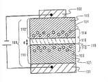
Among Fig. 1, add the first dopant (adopting fluorescent material here) 123 by the hole transporting layer 111 that forms to hole transporting material 121 and form the first light-emitting zone 113.In addition, add the second dopant (phosphor material) 124 by the electron supplying layer 112 that forms to electron transport materials 122 and form the second light-emitting zone 114.In addition, the emission wavelength of the second dopant (phosphor material) 124 constitutes the wavelength than the first dopant 123 length.And, between the first light-emitting zone 113 and the second light-emitting zone 114 with the thickness d setting do not add the second dopant (phosphor material) 124 the layer 116 (hereinafter referred to as " wall "), this point is different from Fig. 9.Here, make wall 116 have electron transport.In addition, the 101st, anode, the 102nd, negative electrode, the 103rd, electroluminescence layer.
At this moment, because wall 116 has electron transport, thereby the recombination region in should constructing is near the interface 115 of the first light-emitting zone 113 and wall 116.And, shown in Fig. 2 (a), because apart from d, the HOMO energy level 201 of the second dopant (phosphor material) can not the direct capture hole.Thereby at first, the first dopant 123 is energized.Energized condition is a heavy attitude energized condition S
D1With triplet energized condition T
D1
Here, shown in Fig. 2 (b), be d because wall 116 makes the distance of the first dopant and the second dopant (phosphor material), thereby aforementioned S
D1→ T
D2The contribution of Foerster type energy transferase 12 11 diminish (along with distance d becomes large and sharp-decay).This part becomes S
D1→ G
D1The i.e. luminous h γ of the first dopant
D1Be observed.
On the other hand, the first dopant adopts fluorescent material here, thereby triplet energized condition T
D1Can not be luminous, but can be to the triplet energized condition T of the second dopant (phosphor material)
D2Carrying out energy shifts.Because the excitation life-span of triplet excitation molecule, excitation life-span length, its diffusion length than a heavy attitude excitation molecule was large usually, thus with aforementioned S
D1→ T
D2Energy transferase 12 11 compare T
D1→ T
D2Energy transferase 12 12 be not subject to impact apart from d.Thereby, even leave to a certain degree apart from d, T
D1→ T
D2Energy shift still effective, the triplet energized condition T of the second dopant (phosphor material) then
D2Be transformed into rapidly luminous h γ
D2
As mentioned above, by adopting element of the present invention structure, can make the first dopant and compare luminous second dopant (phosphor material) that can show more close long wavelength side with the first dopant all luminous, thereby realize white luminous.
In addition, in the element structure shown in Figure 1, phosphor material still also can adopt separately phosphor material as dopant in the second light-emitting zone.
In addition, the luminous element in the first light-emitting zone can adopt phosphor material, but preferably adopts as shown in Figure 1 fluorescent material.Because this moment, a heavy attitude energized condition that produces is mainly at the first light-emitting zone, and the triplet energized condition of generation is made contributions to luminous respectively at the second light-emitting zone, therefore the energized condition that makes heavy attitude/triplet both sides all has a contribution to luminous, can expect the raising of efficient.In addition, luminous principle is understood easily, and element design is also carried out easily.
And in the first light-emitting zone of the present invention, can not adopt dopant yet and adopt separately luminescent layer.But, adopt dopant usually to make luminous efficiency high, thereby preferably adopt as illustrated in fig. 1 dopant.In addition, as mentioned above, because the luminous element in the first light-emitting zone preferably adopts fluorescent material, thereby also preferably adopt fluorescent material as dopant in the first light-emitting zone.This occasion, the kind of dopant can be plural.
In addition, element structure shown in Figure 1 is an example of the present invention, but as long as do not depart from purport of the present invention, is not limited to this.For example among Fig. 1, also can adopt hole transporting layer 111 doping the second dopants (phosphor material), the formation (namely this occasion second light-emitting zone is that 113, the first light-emitting zones are 114) of electron supplying layer 112 doping the first dopant.This occasion must be made of the material of cavity conveying wall 116, at the recombination region of the interface charge carrier of wall 116 and electron supplying layer 112.
In addition, although Fig. 1 is not shown, between anode 101 and hole transporting layer 111, the hole transporting layer that also can insert hole injection layer or be formed by the hole transporting material beyond the hole transporting material 121.And, between negative electrode 102 and electron supplying layer 112, the electron supplying layer that also can insert electron injecting layer or be formed by the electron transport materials beyond the electron transport materials 122.
But, as mentioned above, among the present invention, be conceived in the first light-emitting zone, at first form energized condition, partly shift to the second light-emitting zone energy.From this viewpoint, structure preferably is designed to the first light-emitting zone 113 than the second light-emitting zone 114 more close anode-side as shown in Figure 1.This is because at this moment, by adopting hole blocking layer that hole barrier materials forms as wall 116, can effectively the hole be closed in the hole transporting layer 111, thereby the recombination region of charge carrier can be defined as the first light-emitting zone 113.
In addition, the ionization potential energy value that has the material of maximum ion potential energy in the ionization potential energy value of hole barrier materials and the material that the first light-emitting zone 113 comprises is compared, preferably more than the large 0.4eV.In addition, such as Fig. 1, when the first light-emitting zone 113 comprised dopant, the ionization potential energy value of the hole barrier materials that in fact adopts in the wall 116 was that the ionization potential energy value (preferably more than the large 0.4eV) of hole transporting material 121 is very important greater than the main body in the first light-emitting zone.
By such element design, in the first light-emitting zone, at first form energized condition and partly shift to the second light-emitting zone energy and become easily, but this energy shifts about then must setting apart from d.
At first, be more than the 1nm by making d, can prevent that the energy of Dixter type from shifting (energy that the exchange of the surge movement of electronics causes shifts), the mechanism that energy shifts only is the Foerster type, applicable above-mentioned principle.In addition, if apart from about 30nm, the T that illustrates of Fig. 2 (b) then
D1→ T
D2Energy shift the tendency that violent decay is also arranged.Thereby the proper range of d is below the above 30nm of 1nm.
But for the phosphor material direct capture hole (with reference to Fig. 2 (a)) that prevents the second light-emitting zone, d is preferably in more than the 5nm.In addition, in order to reduce the S among Fig. 2 (b)
D1→ T
D2Energy transferase 12 11 contribution and enough evoke T
D1→ T
D2The suitable distance of energy transferase 12 12 be about 5~20nm.Thereby d is preferably in below the above 20nm of 5nm.
More than, the principle of white organic light emitting element that can realize importing the phosphor material of red colour system by the present invention has been described.Then, to make illuminant colour be the optimal wavelength scope of high-quality white to illustration.
At first, luminous frequency spectrum in the first light-emitting zone has at least one peak value by the zone below the above 500nm of 400nm, or the zone below the above 560nm of 400nm has at least two peak values, can with the second light-emitting zone in the illuminant colour combination of phosphor material of red colour system, realize white light.At this moment, the luminous frequency spectrum of above-mentioned phosphor material is that zone below the above 700nm of 560nm has at least one peak value and gets final product at red colour system.
In addition, for example, if but add the first luminous dopant of excimers at the first light-emitting zone, then by optimizing doping content, it is luminous to carry out simultaneously the intrinsic luminous and excimers of the first dopant.Because excimers are luminous and above-mentionedly intrinsic luminously compare inevitable more close long wavelength side, thereby can draw two luminescence peaks from a material.By making up the illuminant colour of the red colour system in this phenomenon and the second light-emitting zone, the luminous frequency spectrum that has peak value in each wavelength region may of R, G, B also becomes possibility.
Below illustration is used for material of the present invention particularly.But, be not limited to this applicable to material of the present invention.
As the hole-injecting material that is used for hole injection layer, so long as organic compound, then the compound of porphyrin system is all effective, can adopt phthalocyanine (to be called for short: H
2-Pc), the copper phthalocyanine (is called for short: Cu-Pc) etc.In addition, in Electroconductivity of Conducting Polymers, carry out in addition the material of chemical doping, can adopt the poly-p styrene sulfonic acid that mixes (be called for short: poly-dioxoethyl thiophene PSS) (be called for short: PEDOT) or polyaniline (be called for short: PAni), polyvinylcarbazole (is called for short: PVK) etc.In addition, the ultrathin membrane of the inorganic insulator such as vanadium pentoxide or aluminium oxide is also effective.
As hole transporting material, the compound of aromatic amine system (that is the material that, has the combination of phenyl ring-nitrogen) is suitable.As the material of extensive employing, for example, N is arranged, N '-two (3-aminomethyl phenyl)-N, N '-diphenyl-1,1 '-biphenyl-4,4 '-diamines (be called for short: TPD) or derivatives thereof 4,4 '-two [N-(1-naphthyl)-N-phenyl amino] biphenyl (be called for short: α-NPD) etc.In addition, " three (N, N-diphenyl amino) triphenylamine (is called for short: TDATA) or 4,4 ', 4 " three (N-3-aminomethyl phenyl-N-phenyl amino) triphenylamine (is called for short: star array type aromatic amine compound MTDATA) etc. to also have 4,4 ', 4.
As electron transport materials, three (alcoholization of 8-quinoline) aluminium (is called for short: Alq
3), three (4-methyl-8-quinoline alcoholization) aluminium (is called for short: Almq
3), two (10-hydroxy benzo [h] quinoline) beryllium (is called for short: BeBq
2), two (2-methyl-8-quinoline alcoholization)-(4-hydroxyl-xenyl) aluminium (are called for short: BAlq), two [2-(2-hydroxy phenyl)-benzoxazole] zinc (is called for short: Zn (BOX)
2), two [2-(2-hydroxy phenyl)-benzothiazole) zinc (is called for short: Zn (BTZ)
2) etc. metal complex.And, except metal complex, can adopt 2-(4-xenyl)-5-(4-tert-butyl-phenyl)-1,3, the 4-oxadiazole (is called for short: PBD), 1,3-two [5-(to tert-butyl-phenyl)-1,3,4-oxadiazole-2-yl] benzene (is called for short: OXD-7) oxadiazole derivative such as Deng, 3-(4-tert-butyl-phenyl)-4-phenyl-5-(4-xenyl)-1,2, the 4-triazole (is called for short: TAZ), 3-(4-tert-butyl-phenyl)-4-(4-ethylphenyl)-5-(4-xenyl)-1,2, the 4-triazole (is called for short: the triazole derivative such as p-EtTAZ), 2,2 ', 2 " (1,3; 5-benzene three bases (benzenetrilyl)) three [1-phenyl-1H-benzimidazole] (be called for short: the imdazole derivatives such as TPBI); bathophenanthroline (be called for short: BPhen), 2,9-dimethyl-4; 7-diphenyl-1, the 10-phenanthroline (is called for short: the phenanthroline derivative such as BCP).
In addition, the effective hole barrier materials of material as being used for above-mentioned wall can adopt above-mentioned BAlq, OXD-7, TAZ, p-EtTAZ, TPBI, Bphen, BCP etc.
In addition, as the luminous element in the first light-emitting zone, the fluorescent material that also can adopt above-mentioned TPD, α-NPD etc. to have cavity conveying, or Alq
3, Almq
3, BeBq
2, BAlq, Zn (BOX)
2, Zn (BTZ)
2Deng the fluorescent material with electron transport.In addition, various fluorchromes also can be used as dopant, for example quinacridone, N, N '-diformazan quinacridone, perylene, fluoranthene, coumarin series pigment (coumarin 6 etc.) etc.And, also can adopt phosphor material, (be called for short: Ir (ppy) such as three (2-phenylpyridine) Ir
3) etc.These all can present luminescence peak below the above 560nm of 400nm, thereby are suitable as the luminous element in the first light-emitting zone of the present invention.
On the other hand, as the luminous element in the second light-emitting zone, the metal-organic complex of metal is effective centered by iridium or platinum.Particularly, except aforementioned PtOEP, also have two (2-(2 '-benzothiophene) pyridine-N, C
3') (pentanedione acid) iridium (abbreviation: btp
2Ir (acac)), two (2-(2 '-thienyl) pyridine-N, C
3') (pentanedione acid) iridium (abbreviation: thp
2Ir (acac)), two (2-(1-naphthyl) benzoxazole-N, C
2') (pentanedione acid) iridium (abbreviation: bon
2Ir (acac)) etc.These all are the phosphor materials that has luminescence peak at red colour system (below the above 700nm of 560nm), are suitable as the luminous element in the second light-emitting zone of the present invention.
In addition, when the first light-emitting zone of the present invention or the second light-emitting zone use dopant, as material of main part, can adopt hole transporting material or electron transport materials take above-mentioned example as representative.In addition, also can adopt 4,4 '-N, N '-two carbazyl biphenyl (is called for short: bipolar materials CBP) etc.
In addition, among the present invention, each in the organic illuminating element layer is not limited to layered manner.Can be stacked, also can select the various methods such as vacuum vapour deposition or spin-coating method, ink-jet method, dip coating.
(embodiment)
[embodiment 1]
In the present embodiment, with Fig. 3 specifically the thickness d of explicit order wall be the organic illuminating element of the present invention of 10nm.In addition, among Fig. 3,301 are equivalent to anode, and 302 are equivalent to negative electrode, and 303 are equivalent to the electroluminescence layer.
At first, be on the glass substrate of ITO with 100nm left and right sides film forming at anode 301, evaporation 20nm hole transporting material is CuPc, as hole injection layer 310.Then, evaporation 30nm hole transporting material is that α-NPD is as hole transporting layer 311, but carry out common evaporation among its last 10nm, make α-NPD (material of main part) and a heavy attitude luminescent material Ji perylene (guest materials) form about 99: 51 ratio (weight ratio).That is, at the concentration Fen San perylene of α-NPD with about 1wt%.The common evaporation layer of this 10nm is the first light-emitting zone 313.
After the first light-emitting zone 313 formed, hole barrier materials (and electron transport materials) was that BAlq is with the 10nm film forming, as wall 316.And evaporation 30nmBAlq is as electron supplying layer 312, but among its initial 10nm, forms the zone of having added phosphor material PtOEP by common evaporation.Addition is adjusted in BAlq with the concentration of about 7.5wt% and disperses PtOEP.It becomes the second light-emitting zone 314.More than, adopt the layer of BAlq to comprise wall 316 and electron supplying layer 312, amount to 40nm.
Then, electron transport materials is that Alq is with the 20nm film forming, as the second electron supplying layer 317.Then, evaporation 2nm calcirm-fluoride (is called for short: CaF
2) as electron injecting layer 318, last Al with the 150nm film forming as negative electrode.Thereby, obtain organic illuminating element of the present invention.
The characteristic of the organic illuminating element that present embodiment 1 is made is that brightness is 10[cd/m
2] time driving voltage be 8.0[V], current efficiency is 4.7[cd/A].
In addition, Fig. 4 (a) expression 10[cd/m
2] time luminous frequency spectrum.Near 460nm and the 480nm and near the 520nm respectively clear and definite Guan Ce Dao the frequency spectrum 402 of the luminous green that causes of excimers of the luminous frequency spectrum 401 He perylenes of the intrinsic blueness of perylene.In addition, near 650nm, observe the peak value 403 of the sharp-pointed redness that PtOEP causes.
Like this, in the present embodiment 1, each wavelength region may that adopts the phosphor material of red colour system can be implemented in R, G, B has the organic illuminating element of peak value.In addition, the cie color coordinate is (x, y)=(0.30,0.35), looks like white luminous.
More than, in the present embodiment 1, can to a certain degree suppress S shown in Fig. 2 (b)
D1→ T
D2Energy shift , Shi perylene and PtOEP two can be luminous.
In addition, for the α-NPD of hole transporting layer 311 employings and the BAlq of wall 315 employings, when measuring respectively ionization potential energy (be respectively under the state of film and measure with photoelectron light-dividing device AC-2 (reason is ground instrument)), α-NPD is 5.3[eV], BAlq is 5.7[eV].That is, consider that both ionization potential energy differs about 0.4[eV], thereby BAlq blocking hole effectively is controlled at (or in first light-emitting zone 313) in the hole transporting layer 311 with the recombination region of charge carrier.
[embodiment 2]
In the present embodiment, the thickness d that makes wall is that the organic illuminating element of the present invention of 20nm is with Fig. 3 illustration particularly.
At first, till the first light-emitting zone 313, form similarly to Example 1.After the first light-emitting zone 313 formed, hole barrier materials (and electron transport materials) was that BAlq is with the 20nm film forming, as wall 316.And evaporation 20nmBAlq is as electron supplying layer 312, but the zone of adding phosphor material PtOEP by being total to evaporation formation among its initial 10nm.Addition is adjusted in BAlq with the concentration of about 7.5wt% and disperses PtOEP.It is as the second light-emitting zone 314.More than, adopt the layer of BAlq to comprise wall 316 and electron supplying layer 312, amount to 40nm.
Then, electron transport materials is that Alq is with the 20nm film forming, as the second electron supplying layer 317.Then, the CaF of evaporation 2nm
2As electron injecting layer 318, last Al with the 150nm film forming as negative electrode.Thereby, obtain organic illuminating element of the present invention.
The characteristic of the organic illuminating element that present embodiment 2 is made is that brightness is 10[cd/m
2] time driving voltage be 8.6[V], current efficiency is 4.6[cd/A].
In addition, Fig. 4 (b) expression 10[cd/m
2] time luminous frequency spectrum.Near 460nm and the 480nm and near the 520nm respectively clear and definite Guan Ce Dao the frequency spectrum 402 of the luminous green that causes of excimers of the luminous frequency spectrum 401 He perylenes of the intrinsic blueness of perylene.In addition, near 650nm, observe the peak value 403 of the sharp-pointed redness that PtOEP causes.
Like this, in the present embodiment 2, each wavelength region may that adopts the phosphor material of red colour system can be implemented in R, G, B has the organic illuminating element of peak value.In addition, the cie color coordinate is (x, y)=(0.25,0.36), looks like the white luminous of little aobvious blueness.
More than, in the present embodiment 2, can suppress S shown in Fig. 2 (b) fully
D1→ T
D2Energy shift , Shi perylene and PtOEP two can be luminous.
[embodiment 3]
In the present embodiment, the thickness d that makes wall is that the organic illuminating element of the present invention of 30nm is with Fig. 3 illustration particularly.
At first, till the first light-emitting zone 313, similarly form with embodiment 1 or embodiment 2.After the first light-emitting zone 313 formed, hole barrier materials (and electron transport materials) was that BAlq is with the 30nm film forming, as wall 316.And, common evaporation is carried out in the zone of adding phosphor material PtOEP in BAlq, form the second light-emitting zone 314 of 10nm.Addition is adjusted in BAlq with the concentration of about 7.5wt% and disperses PtOEP.More than, adopt the layer of BAlq to comprise wall 316 and the second light-emitting zone 314, amount to 40nm.In the present embodiment, again BAlq is not formed electron supplying layer 312 (this is to be similarly 40nm for the thickness that makes the layer that adopts BAlq and embodiment 1 and embodiment 2) behind the second light-emitting zone 314.
Then, electron transport materials is that Alq is with the 20nm film forming, as the second electron supplying layer 317.Then, the CaF of evaporation 2nm
2As electron injecting layer 318, last Al with the 150nm film forming as negative electrode.Thereby, obtain organic illuminating element of the present invention.
The characteristic of the organic illuminating element that present embodiment 3 is made is that brightness is 10[cd/m
2] time driving voltage be 8.2[V], current efficiency is 4.6[cd/A].
In addition, Fig. 4 (c) expression 10[cd/m
2] time luminous frequency spectrum.Near 460nm and the 480nm and near the 520nm respectively clear and definite Guan Ce Dao the frequency spectrum 402 of the luminous green that causes of excimers of the luminous frequency spectrum 401 He perylenes of the intrinsic blueness of perylene.The peak value 403 of the sharp-pointed redness that near the PtOEP a little less than in addition, observing 650nm causes.
Like this, in the present embodiment 3, each wavelength region may that adopts the phosphor material of red colour system can be implemented in R, G, B has the organic illuminating element of peak value.In addition, the cie color coordinate is (x, y)=(0.22,0.35), looks like the white luminous of little aobvious blueness.
More than, in the present embodiment 3, can almost completely suppress S shown in Fig. 2 (b)
D1→ T
D2Energy shift, compare T with embodiment 1 or embodiment 2
D1→ T
D2Energy shift decay Wei as a result the luminous grow of perylene, the luminous of PtOEP dies down.Thereby the thickness d of wall of the present invention preferably is not higher than 30nm.
[comparative example 1]
In this comparative example, traditional organic illuminating element of not establishing wall specifically describes with Figure 11.In addition, quote the symbol of Fig. 3 among Figure 11.
At first, till the first light-emitting zone 313, form equally with embodiment 1~embodiment 3.After the first light-emitting zone 313 forms, BAlq with the 40nm film forming as electron supplying layer 312, but form the second light-emitting zone 314 that adds phosphor material PtOEP take BAlq as main body among its initial 10nm.Addition is adjusted in BAlq with the concentration of about 7.5wt% and disperses PtOEP.
Then, electron transport materials Alq is with the 20nm film forming, as the second electron supplying layer 317.Then, the CaF of evaporation 2nm
2As electron injecting layer 317, last Al with the 150nm film forming as negative electrode.
The characteristic of the organic illuminating element that this comparative example is made is that brightness is 10[cd/m
2] time driving voltage be 8.8[V], current efficiency is 1.9[cd/A].
In addition, 10[cd/m
2] time luminous frequency spectrum as shown in figure 12.In this comparative example, almost can not see the luminous frequency spectrum of surveying perylene, can only observe the peak value 1201 of the sharp-pointed redness that near the PtOEP the 650nm causes.In addition, the cie color coordinate is (x, y)=(0.51,0.33), seems to be roughly redness.
More than, shown in this comparative example, do not establish in the traditional element structure of wall of the present invention, be difficult to realize adopt the white organic light emitting element of the phosphor material of red colour system.
[embodiment 4]
In the present embodiment, possesses the light-emitting device of organic illuminating element of the present invention in pixel section with Fig. 5 explanation.In addition, Fig. 5 (A) is the vertical view of light-emitting device, and Fig. 5 (B) is the sectional view along the A-A ' cut-out of Fig. 5 (A).The 501st, drive circuit section (source side drive circuit), the 502nd, pixel section, the 503rd, drive circuit section (gate side drive circuit).In addition, the 504th, seal substrate, the 505th, sealant, the inboard 507 that sealant 505 surrounds forms the space.
In addition, the 508th, the connection distribution that the signal of transmission input source electrode side drive circuit 501 and gate side drive circuit 503 is used is from the sub-FPC of external input terminals (flexible print circuit) 509 receiving video signals, clock signal, commencing signal, reset signal etc.In addition, only illustrate FPC here, printing distributing board (PWB) also can be installed among this FPC.Light-emitting device in this specification not only comprises the light-emitting device body, also comprises the state that FPC or PWB wherein are installed.
Then, with Fig. 5 (B) cross-sectional configuration is described.Form drive circuit section and pixel section at substrate 510, shown that here drive circuit section is source side drive circuit 501 and pixel section 502.
In addition, in the source side drive circuit 501, form the cmos circuit by n channel-type TFT523 and p channel-type TFT524 combination.In addition, the TFT of formation drive circuit also can be formed by known cmos circuit, PMOS circuit or nmos circuit.In addition, in this example, represented to form at substrate driver one-piece type of drive circuit, but dispensable, also can not on substrate, externally form.
In addition, pixel section 502 forms with TFT512 with a plurality of pixels of the 1st electrode 513 of its drain electrode electrical connection with TFT511 and Current Control by comprising switch.In addition, form the insulant 514 of the end that covers the 1st electrode 513.Here, adopt the photonasty acrylic resin film of positive type to form.
In order to form good coating, the curved surface that is formed with curvature in upper end or the bottom of insulant 514.For example, the material of insulant 514 adopts the acrylic acid occasion of photonasty of positive type, preferably only possesses the curved surface of radius of curvature (0.2 μ m~3 μ m) in the upper end of insulant 514.In addition, as insulant 514, can use by photosensitive light becomes the negative-type that is insoluble to etching agent or becomes one of positive type that is dissolved in etching agent by light.
On the 1st electrode 513, form respectively electroluminescence layer 515 and the 2nd electrode 516.Here, the material that plays the 1st electrode 513 of anode function preferably adopts the large material of working function.For example, the monofilm of ITO (tin indium oxide) film, indium zinc oxide (IZO) film, titanium nitride film, chromium film, tungsten film, Zn film, Pt film etc. also can adopt stacked, the titanium nitride film of film take titanium nitride and aluminium as principal component and 3 layers of structure of the film take aluminium as principal component and titanium nitride film etc.If the employing lit-par-lit structure, then the resistance as distribution is also low, and can obtain good ohmic contact, and plays the function of anode.Here with ITO as the first electrode 513, adopt the structure from substrate 510 side-draw bright dippings.
In addition, electroluminescence layer 515 forms by vapour deposition method or the ink-jet method that adopts the evaporation mask.Electroluminescence layer 515 also can adopt the electroluminescence layer with structure disclosed by the invention.Be specially the formation of the electroluminescence layer of embodiment 1~embodiment 3 explanations.In addition, the material of electroluminescence layer adopts individual layer or stacked organic compound usually, but the present invention is also included within the formation that the part of the film of organic compound composition adopts inorganic compound.
And the material of the 2nd electrode (negative electrode) 516 that forms on the electroluminescence layer 515 can adopt the little material of working function (Al, Ag, Li, Ca or these alloy MgAg, MgIn, AlLi, CaF
2Or CaN).In addition, during light transmission the 2nd electrode 516 of electroluminescence layer 515 generation, the 2nd electrode (negative electrode) 516 preferably adopts the stacked of the thin metallic film of thickness and nesa coating (ITO, IZO, zinc oxide (ZnO) etc.).Here, adopt the non-film that sees through of Al, form from the light-emitting device of the bottom surface outgoing type structure of substrate 510 side-draw bright dippings.
And with sealant 505 adhesive seal substrates 504 and component substrate 510, the space 507 that is formed on substrate 501, seal substrate 504 and sealant 505 encirclements possesses the structure of organic illuminating element 517 of the present invention.In addition, space 507 also comprises the formation of filling with sealant 505 except filling with inert gas (nitrogen or argon etc.).
In addition, sealant 505 preferably adopts epoxy resin.In addition, these materials preferably do not see through the material of moisture or oxygen as far as possible.In addition, as the material of seal substrate 504, the plastic that can adopt glass substrate or quartz substrate and FRP (Fiberglass-Reinforced Plastics), PVF (polyvinyl fluoride), Mu La (Mylar), polyester or acrylic acid etc. to form.
More than can obtain to have the light-emitting device of organic illuminating element of the present invention.
[embodiment 5]
Specifically describe in the present embodiment in light-emitting device shown in Figure 5, from the light-emitting device of the end face outgoing type of seal substrate 504 side-draw bright dippings structure.Its skeleton diagram (sectional view) is shown in Fig. 6 (A).In addition, quote the symbol of Fig. 5 among Fig. 6 (A).Light emission direction represents with 621 in Fig. 6 (A).
Among Fig. 6 (A), the 1st electrode 513 adopts the anode of light-proofness, and the 2nd electrode adopts the negative electrode of light transmission, forms end face outgoing structure.Thereby the 1st electrode can adopt the monofilm of titanium nitride film, chromium film, tungsten film, Zn film, Pt film etc., also can adopt stacked, the titanium nitride film of film take titanium nitride and aluminium as principal component and 3 layers of structure of the film take aluminium as principal component and titanium nitride film etc.In addition, the 2nd electrode can adopt the lit-par-lit structure of the thin metallic film of thickness and nesa coating (ITO, IZO, ZnO etc.).Here, the 1st electrode adopts titanium nitride film, and the 2nd electrode adopts the lit-par-lit structure of Mg:Ag alloy firm and ITO.
In addition, the light-emitting device of present embodiment is in order to adopt white organic light emitting element 517 of the present invention carry out panchromaticization, and the colour filter that dyed layer 611 and light shield layer (BM) 612 form (in order to simplify, here not shown external coating) is set.
In addition, in order to seal organic illuminating element 517, form protective clear layer 601.This protective clear layer 601 preferably adopts the silicon nitride of sputtering method (DC mode or RF mode) or the acquisition of PCVD method or the dielectric film, (diamond-film-like: DLC film of the film take carbon as principal component that silicon oxynitride is principal component; carbonitride: CN film etc.), or these is stacked.Adopt silicon target, under the atmosphere that comprises nitrogen and argon, can obtain the high silicon nitride film of impurity blocking effect to moisture or alkali metal etc.In addition, also can adopt silicon nitride target.In addition, protective clear layer also can adopt the isoionic film formation device of remote control to form.In addition, luminous by protective clear layer in order to make, the thickness of protective clear layer is preferably thin as far as possible.
Here, in order further to seal organic illuminating element 517, not only adopt sealant 505, also adopt the space 507 in the 2nd sealant 602 blank maps 5, paste with seal substrate 504.Sealing operates under the inert gas atmosphere and gets final product.The 2nd sealant 602 is same with sealant 505, preferably adopts epoxy resin.
[embodiment 6]
Specifically describe in the present embodiment in light-emitting device shown in Figure 5, take out the light-emitting device of the two sides outgoing type structure of light from two sides of substrate 510 sides and seal substrate 504 sides.Its skeleton diagram (sectional view) is shown in Fig. 6 (B).In addition, Fig. 6 (B) quotes the symbol of Fig. 5.Light emission direction represents with 622,623 in Fig. 6 (B).
Essential structure among Fig. 6 (B) is identical with Fig. 6 (A), is to adopt the nesa coating of ITO film or IZO film etc. as the 1st electrode 513 with the difference of Fig. 6 (A).Here, adopt the ITO film can realize the light-emitting device of two sides outgoing structure.
In addition, among Fig. 6 (B), substrate 510 sides do not arrange colour filter, make all panchromaticization of two sides but colour filter also can be set.This occasion, the colour filter that substrate 510 sides form can similarly arrange with the method for traditional employings such as liquid crystal indicator.
[embodiment 7]
In the present embodiment, the various electronic equipments of finishing with the light-emitting device with organic illuminating element of the present invention are described.
Electronic equipment with the light-emitting device making with organic illuminating element of the present invention, gamma camera, digital camera, glasses type display (Helmet Mounted Display), navigation system, sound equipment regenerating unit (automobile audio, audible component etc.) are arranged, subnotebook PC, game station, portable information terminal (pocket computer, portable phone, pocket game machine or e-book etc.), possess image-reproducing apparatus (being specially the recording medium that possesses renewable DVD etc. and the device that shows the display of its image) of recording medium etc.The concrete example of these electronic equipments is shown in Fig. 7,8.
Fig. 7 (A) is display unit, comprises framework 7101, supports platform 7102, display part 7103, loud speaker section 7104, video input terminal 7105 etc.Has the light-emitting device of organic illuminating element of the present invention applicable to this display part 7103.In addition, display unit comprises PC and broadcasts to receive with, TV and show with, advertisement that all information of using etc. show and use devices.
Fig. 7 (B) is subnotebook PC, comprises body 7201, framework 7202, display part 7203, keyboard 7204, external connection port 7205, mouse 7206 etc.Has the light-emitting device of organic illuminating element of the present invention applicable to this display part 7203.
Fig. 7 (C) is pocket computer, comprises body 7301, display part 7302, switch 7303, operation keys 7304, infrared port 7305 etc.Has the light-emitting device of organic illuminating element of the present invention applicable to this display part 7302.
Fig. 7 (D) is the image regenerating device (being specially the DVD regenerating unit) that possesses the pocket of recording medium, comprises body 7401, framework 7402, display part A7403, display part B7404, recording medium (DVD etc.) is read in section 7405, operation keys 7406, loud speaker section 7407 etc.Display part A7403 mainly shows pictorial information, and the main display text information of display part B7404 has the light-emitting device of organic illuminating element of the present invention applicable to these display parts A, B.In addition, the image regenerating device that possesses recording medium also comprises home-use game station etc.
Fig. 7 (E) is glasses type display (helmet-mounted display), comprises body 7501, display part 7502, arm 7503.Has the light-emitting device of organic illuminating element of the present invention applicable to this display part 7502.
Fig. 7 (F) is gamma camera, comprises body 7601, display part 7602, framework 7603, external connection port 7604, remote control reception section 7605, is subjected to picture section 7606, battery 7607, Speech input section 7608, operation keys 7609, connects eye 7610 etc.Has the light-emitting device of organic illuminating element of the present invention applicable to this display part 7602.
Fig. 7 (G) is portable phone, comprises body 7701, framework 7702, display part 7703, Speech input section 7704, audio output unit 7705, operation keys 7706, external connection port 7707, antenna 7708 etc.Has the light-emitting device of organic illuminating element of the present invention applicable to this display part 7703.In addition, display part 7703 can suppress the current sinking of portable phone at the literal of the background display white of black.
Fig. 8 a is lighting at two sides type notebook PC, comprises keypad portion 801, display section 802 etc.The feature of this notebook PC can be to surface light emitting 803 with to back side illuminated 804 shown in Fig. 8 b.Can be applicable to display section 802 by for example light-emitting device of the two sides of the present invention outgoing structure shown in Fig. 6 (B) realizes.By such formation, shown in Fig. 8 c, even display section 802 also can utilize the luminous image etc. of watching to the back side for closed condition.The display section direction of spreading its tail represents with 805.
Utilize possibility on the industry
As mentioned above, have being of wide application of light-emitting device of organic illuminating element of the present invention, this light-emitting device is applicable to the electronic equipment in each field.