CN101418931B - Backlight assembly - Google Patents
Backlight assembly Download PDFInfo
- Publication number
- CN101418931B CN101418931B CN2008102131134A CN200810213113A CN101418931B CN 101418931 B CN101418931 B CN 101418931B CN 2008102131134 A CN2008102131134 A CN 2008102131134A CN 200810213113 A CN200810213113 A CN 200810213113A CN 101418931 B CN101418931 B CN 101418931B
- Authority
- CN
- China
- Prior art keywords
- light
- emitting diode
- guide plate
- diode array
- emitting diodes
- Prior art date
- Legal status (The legal status is an assumption and is not a legal conclusion. Google has not performed a legal analysis and makes no representation as to the accuracy of the status listed.)
- Active
Links
Images




Classifications
-
- G—PHYSICS
- G02—OPTICS
- G02F—OPTICAL DEVICES OR ARRANGEMENTS FOR THE CONTROL OF LIGHT BY MODIFICATION OF THE OPTICAL PROPERTIES OF THE MEDIA OF THE ELEMENTS INVOLVED THEREIN; NON-LINEAR OPTICS; FREQUENCY-CHANGING OF LIGHT; OPTICAL LOGIC ELEMENTS; OPTICAL ANALOGUE/DIGITAL CONVERTERS
- G02F1/00—Devices or arrangements for the control of the intensity, colour, phase, polarisation or direction of light arriving from an independent light source, e.g. switching, gating or modulating; Non-linear optics
- G02F1/01—Devices or arrangements for the control of the intensity, colour, phase, polarisation or direction of light arriving from an independent light source, e.g. switching, gating or modulating; Non-linear optics for the control of the intensity, phase, polarisation or colour
- G02F1/13—Devices or arrangements for the control of the intensity, colour, phase, polarisation or direction of light arriving from an independent light source, e.g. switching, gating or modulating; Non-linear optics for the control of the intensity, phase, polarisation or colour based on liquid crystals, e.g. single liquid crystal display cells
- G02F1/133—Constructional arrangements; Operation of liquid crystal cells; Circuit arrangements
- G02F1/1333—Constructional arrangements; Manufacturing methods
- G02F1/1335—Structural association of cells with optical devices, e.g. polarisers or reflectors
-
- G—PHYSICS
- G02—OPTICS
- G02B—OPTICAL ELEMENTS, SYSTEMS OR APPARATUS
- G02B6/00—Light guides; Structural details of arrangements comprising light guides and other optical elements, e.g. couplings
- G02B6/0001—Light guides; Structural details of arrangements comprising light guides and other optical elements, e.g. couplings specially adapted for lighting devices or systems
- G02B6/0011—Light guides; Structural details of arrangements comprising light guides and other optical elements, e.g. couplings specially adapted for lighting devices or systems the light guides being planar or of plate-like form
- G02B6/0013—Means for improving the coupling-in of light from the light source into the light guide
- G02B6/0023—Means for improving the coupling-in of light from the light source into the light guide provided by one optical element, or plurality thereof, placed between the light guide and the light source, or around the light source
-
- G—PHYSICS
- G02—OPTICS
- G02B—OPTICAL ELEMENTS, SYSTEMS OR APPARATUS
- G02B6/00—Light guides; Structural details of arrangements comprising light guides and other optical elements, e.g. couplings
- G02B6/0001—Light guides; Structural details of arrangements comprising light guides and other optical elements, e.g. couplings specially adapted for lighting devices or systems
- G02B6/0011—Light guides; Structural details of arrangements comprising light guides and other optical elements, e.g. couplings specially adapted for lighting devices or systems the light guides being planar or of plate-like form
-
- G—PHYSICS
- G02—OPTICS
- G02F—OPTICAL DEVICES OR ARRANGEMENTS FOR THE CONTROL OF LIGHT BY MODIFICATION OF THE OPTICAL PROPERTIES OF THE MEDIA OF THE ELEMENTS INVOLVED THEREIN; NON-LINEAR OPTICS; FREQUENCY-CHANGING OF LIGHT; OPTICAL LOGIC ELEMENTS; OPTICAL ANALOGUE/DIGITAL CONVERTERS
- G02F1/00—Devices or arrangements for the control of the intensity, colour, phase, polarisation or direction of light arriving from an independent light source, e.g. switching, gating or modulating; Non-linear optics
- G02F1/01—Devices or arrangements for the control of the intensity, colour, phase, polarisation or direction of light arriving from an independent light source, e.g. switching, gating or modulating; Non-linear optics for the control of the intensity, phase, polarisation or colour
- G02F1/13—Devices or arrangements for the control of the intensity, colour, phase, polarisation or direction of light arriving from an independent light source, e.g. switching, gating or modulating; Non-linear optics for the control of the intensity, phase, polarisation or colour based on liquid crystals, e.g. single liquid crystal display cells
- G02F1/133—Constructional arrangements; Operation of liquid crystal cells; Circuit arrangements
- G02F1/1333—Constructional arrangements; Manufacturing methods
-
- G—PHYSICS
- G02—OPTICS
- G02B—OPTICAL ELEMENTS, SYSTEMS OR APPARATUS
- G02B6/00—Light guides; Structural details of arrangements comprising light guides and other optical elements, e.g. couplings
- G02B6/0001—Light guides; Structural details of arrangements comprising light guides and other optical elements, e.g. couplings specially adapted for lighting devices or systems
- G02B6/0011—Light guides; Structural details of arrangements comprising light guides and other optical elements, e.g. couplings specially adapted for lighting devices or systems the light guides being planar or of plate-like form
- G02B6/0033—Means for improving the coupling-out of light from the light guide
- G02B6/005—Means for improving the coupling-out of light from the light guide provided by one optical element, or plurality thereof, placed on the light output side of the light guide
- G02B6/0055—Reflecting element, sheet or layer
-
- G—PHYSICS
- G02—OPTICS
- G02B—OPTICAL ELEMENTS, SYSTEMS OR APPARATUS
- G02B6/00—Light guides; Structural details of arrangements comprising light guides and other optical elements, e.g. couplings
- G02B6/0001—Light guides; Structural details of arrangements comprising light guides and other optical elements, e.g. couplings specially adapted for lighting devices or systems
- G02B6/0011—Light guides; Structural details of arrangements comprising light guides and other optical elements, e.g. couplings specially adapted for lighting devices or systems the light guides being planar or of plate-like form
- G02B6/0066—Light guides; Structural details of arrangements comprising light guides and other optical elements, e.g. couplings specially adapted for lighting devices or systems the light guides being planar or of plate-like form characterised by the light source being coupled to the light guide
- G02B6/0068—Arrangements of plural sources, e.g. multi-colour light sources
-
- G—PHYSICS
- G02—OPTICS
- G02B—OPTICAL ELEMENTS, SYSTEMS OR APPARATUS
- G02B6/00—Light guides; Structural details of arrangements comprising light guides and other optical elements, e.g. couplings
- G02B6/0001—Light guides; Structural details of arrangements comprising light guides and other optical elements, e.g. couplings specially adapted for lighting devices or systems
- G02B6/0011—Light guides; Structural details of arrangements comprising light guides and other optical elements, e.g. couplings specially adapted for lighting devices or systems the light guides being planar or of plate-like form
- G02B6/0066—Light guides; Structural details of arrangements comprising light guides and other optical elements, e.g. couplings specially adapted for lighting devices or systems the light guides being planar or of plate-like form characterised by the light source being coupled to the light guide
- G02B6/0073—Light emitting diode [LED]
Landscapes
- Physics & Mathematics (AREA)
- General Physics & Mathematics (AREA)
- Optics & Photonics (AREA)
- Nonlinear Science (AREA)
- Mathematical Physics (AREA)
- Chemical & Material Sciences (AREA)
- Crystallography & Structural Chemistry (AREA)
- Planar Illumination Modules (AREA)
- Liquid Crystal (AREA)
Abstract
背光组件。本发明提供了一种背光组件。所述背光组件包括包含多个发光二极管的发光二极管阵列、位于发光二极管阵列侧面的导光板、以及支撑所述导光板的支撑件。由位于所述发光二极管阵列两端的发光二极管产生、并入射到所述导光板上的光比由其他发光二极管产生、并入射到所述导光板上的光暗。
backlight assembly. The invention provides a backlight assembly. The backlight assembly includes a light-emitting diode array including a plurality of light-emitting diodes, a light guide plate located on a side of the light-emitting diode array, and a supporting member supporting the light guide plate. The light generated by the light emitting diodes located at both ends of the light emitting diode array and incident on the light guide plate is darker than the light generated by other light emitting diodes and incident on the light guide plate.
Description
技术领域 technical field
本发明的示例性实施方式涉及用于向平板显示器发射光的背光组件。Exemplary embodiments of the present invention relate to a backlight assembly for emitting light to a flat panel display.
背景技术 Background technique
本申请要求2007年10月23日提交的韩国专利申请No.10-2007-0106636的优先权,此处以引证的方式并入其全部内容,就像在此进行了完整阐述一样。This application claims priority from Korean Patent Application No. 10-2007-0106636 filed on October 23, 2007, the entire contents of which are hereby incorporated by reference as if fully set forth herein.
在平板显示器中,液晶显示器控制具有各向异性介电常数的液晶层的分子排列,并控制由液晶层透射的光量,由此显示图像。Among flat panel displays, a liquid crystal display controls molecular alignment of a liquid crystal layer having an anisotropic dielectric constant, and controls the amount of light transmitted by the liquid crystal layer, thereby displaying an image.
因为液晶显示器是光接收型显示器,所以液晶显示器需要产生光的背光组件以显示图像。背光组件包括产生光的光源。光源的示例包括冷阴极荧光灯(CCFL)、外部电极荧光灯(EEFL)、以及发光二极管(LED)。Since the liquid crystal display is a light receiving type display, the liquid crystal display requires a backlight assembly that generates light to display images. The backlight assembly includes a light source that generates light. Examples of light sources include cold cathode fluorescent lamps (CCFLs), external electrode fluorescent lamps (EEFLs), and light emitting diodes (LEDs).
在背光组件包括发光二极管作为光源的情况下,同时使用红、绿、和蓝发光二极管以产生白光。红、绿、和蓝光是光的三原色,并混合在一起以产生白光。如上所述,因为发光二极管利用光的三原色,色彩的表现范围比较宽。In the case where the backlight assembly includes light emitting diodes as light sources, red, green, and blue light emitting diodes are used simultaneously to generate white light. Red, green, and blue light are the three primary colors of light and are mixed together to produce white light. As mentioned above, because light-emitting diodes use the three primary colors of light, the range of color expression is relatively wide.
例如,3色发光二极管组成发光二极管阵列,其中红、绿、和蓝发光二极管按照此顺序排列。红和蓝发光二极管分别位于发光二极管阵列的开始和结束处,并且因此位于发光二极管阵列的开始和结束处的红光的量和蓝光的量相对地比其他光的量多。结果,因为红、绿、和蓝光在发光二极管阵列的开始和结束处不是均匀地混合,在液晶面板的两端处发出添加了红或蓝光的白光。因此,液晶面板的色彩均匀性降低。For example, 3-color LEDs form a LED array, where red, green, and blue LEDs are arranged in this order. Red and blue light emitting diodes are located at the beginning and end of the light emitting diode array, respectively, and thus the amount of red light and the blue light located at the beginning and end of the light emitting diode array are relatively larger than the other lights. As a result, white light to which red or blue light is added is emitted at both ends of the liquid crystal panel because red, green, and blue light are not uniformly mixed at the beginning and end of the light emitting diode array. Therefore, the color uniformity of the liquid crystal panel is lowered.
发明内容 Contents of the invention
本发明示例性实施方式提供一种当发光二极管用作光源时能够在整个区域上产生均匀白光的背光组件。Exemplary embodiments of the present invention provide a backlight assembly capable of generating uniform white light over an entire area when a light emitting diode is used as a light source.
本发明的示例性实施方式的附加特征和优点将在下面的描述中描述且将从描述中部分地显现,或者可以通过本发明的示例性实施方式的实践来了解。通过书面的说明书及其权利要求以及附图中特别指出的结构可以实现和获得本发明的示例性实施方式的目的和其他优点。Additional features and advantages of exemplary embodiments of the invention will be set forth in the description which follows and, in part, will be apparent from the description, or may be learned by practice of the exemplary embodiments of the invention. The objectives and other advantages of the exemplary embodiments of the invention may be realized and attained by the structure particularly pointed out in the written description and claims hereof as well as the appended drawings.
在一方面,一种背光组件包括包含多个发光二极管的发光二极管阵列、位于发光二极管阵列侧面的导光板、以及支撑所述导光板的支撑件。由位于所述发光二极管阵列两端的发光二极管产生、并入射到所述导光板上的光比由其他发光二极管产生、并入射到所述导光板上的光暗。In one aspect, a backlight assembly includes a light-emitting diode array including a plurality of light-emitting diodes, a light guide plate positioned at a side of the light-emitting diode array, and a support member supporting the light guide plate. The light generated by the light emitting diodes located at both ends of the light emitting diode array and incident on the light guide plate is darker than the light generated by other light emitting diodes and incident on the light guide plate.
所述支撑件可包括固定所述导光板的框,以及由所述框的一部分形成、并与位于所述发光二极管阵列的两端的发光二极管相对的遮蔽单元。The supporter may include a frame fixing the light guide plate, and shielding units formed by a part of the frame and facing the LEDs located at both ends of the LED array.
所述发光二极管阵列可包括产生蓝光的第一发光二极管、产生绿光的第二发光二极管、以及产生红光的第三发光二极管。第一至第三发光二极管分别可与产生不同颜色光的发光二极管相邻。The LED array may include a first LED that generates blue light, a second LED that generates green light, and a third LED that generates red light. The first to third light emitting diodes may be respectively adjacent to light emitting diodes that generate light of different colors.
所述背光组件还可包括位于发光二极管阵列和所述导光板之间、并部分地遮蔽位于发光二极管阵列两端的发光二极管的遮蔽单元。The backlight assembly may further include a shielding unit positioned between the LED array and the light guide plate and partially shielding the LEDs positioned at both ends of the LED array.
由位于所述发光二极管阵列两端的发光二极管产生的光的量可少于由其他发光二极管产生的光的量。An amount of light generated by LEDs positioned at both ends of the LED array may be less than an amount of light generated by other LEDs.
位于所述发光二极管阵列两端的发光二极管的外表面被雾化处理,以发出比由其他发光二极管产生的光更暗的光。The outer surfaces of the LEDs located at both ends of the LED array are fogged to emit light that is darker than that produced by the other LEDs.
在另一方面,一种背光组件包括包含多个发光二极管的发光二极管阵列、位于所述发光二极管阵列侧面的导光板、以及用于散射从所述导光板发出的光的光学片,其中产生白光的白发光二极管分别位于所述发光二极管阵列的两端。In another aspect, a backlight assembly includes a light emitting diode array including a plurality of light emitting diodes, a light guide plate positioned at a side of the light emitting diode array, and an optical sheet for diffusing light emitted from the light guide plate, wherein white light is generated The white light-emitting diodes are respectively located at both ends of the light-emitting diode array.
应当理解上述一般描述和下面的详细描述是示例性和说明性的,且旨在提供如权利要求限定的本发明实施方式的进一步解释。It is to be understood that both the foregoing general description and the following detailed description are exemplary and explanatory and are intended to provide further explanation of embodiments of the invention, as claimed.
附图说明 Description of drawings
附图被包括在本说明书中以提供对本发明的进一步理解,并结合到本说明书中且构成本说明书的一部分,附图示出了本发明的实施方式,且与说明书一起用于解释本发明的原理。附图中:The accompanying drawings, which are included in this specification to provide a further understanding of the invention, are incorporated in this specification and constitute a part of this specification, illustrate the embodiments of the present invention, and together with the specification serve to explain the concept of the present invention. principle. In the attached picture:
图1是根据本发明第一示例性实施方式的平板显示器的分解透视图;1 is an exploded perspective view of a flat panel display according to a first exemplary embodiment of the present invention;
图2是根据本发明第一示例性实施方式的平板显示器的截面图;2 is a cross-sectional view of a flat panel display according to a first exemplary embodiment of the present invention;
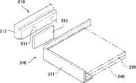
图3是示出发光二极管阵列和支撑件之间的位置关系的局部分解透视图;3 is a partially exploded perspective view showing a positional relationship between a light emitting diode array and a support;
图4是示出发光二极管和支撑件之间的位置关系的示意性平面图;4 is a schematic plan view illustrating a positional relationship between light emitting diodes and a support;
图5是示出根据本发明第一示例性实施方式的液晶面板的光发射的照片;5 is a photograph showing light emission of a liquid crystal panel according to a first exemplary embodiment of the present invention;
图6是示出现有技术液晶面板的光发射的照片;6 is a photograph showing light emission of a prior art liquid crystal panel;
图7是示出遮蔽单元从支撑件分离的局部分解透视图;Fig. 7 is a partially exploded perspective view showing separation of the shielding unit from the support;
图8是示出遮蔽单元、支撑件、以及发光二极管阵列之间位置关系的示意性平面图;8 is a schematic plan view showing the positional relationship among the shielding unit, the support, and the LED array;
图9是示出根据本发明第二示例性实施方式的发光二极管阵列和支撑件之间位置关系的示意性平面图;9 is a schematic plan view illustrating a positional relationship between a light emitting diode array and a support according to a second exemplary embodiment of the present invention;
图10是示出根据本发明第三示例性实施方式的发光二极管阵列和支撑件之间位置关系的示意性平面图;10 is a schematic plan view illustrating a positional relationship between a light emitting diode array and a support according to a third exemplary embodiment of the present invention;
图11示出根据颜色的发光二极管的电连接;以及Figure 11 shows the electrical connections of light emitting diodes according to color; and
图12是白发光二极管的截面图。Fig. 12 is a cross-sectional view of a white light emitting diode.
具体实施方式 Detailed ways
下面将详细描述本发明的实施方式,在附图中示例出了其示例。Reference will now be made in detail to embodiments of the invention, examples of which are illustrated in the accompanying drawings.
图1是根据本发明第一示例性实施方式的液晶显示器的分解透视图。FIG. 1 is an exploded perspective view of a liquid crystal display according to a first exemplary embodiment of the present invention.
如图1所示,根据本发明第一示例性实施方式的液晶显示器包括液晶面板100、位于液晶面板100之下的背光组件、以及用于封装液晶面板100和背光组件的底盖320和顶盖330。As shown in FIG. 1 , the liquid crystal display according to the first exemplary embodiment of the present invention includes a liquid crystal panel 100, a backlight assembly located under the liquid crystal panel 100, and a bottom cover 320 and a top cover for encapsulating the liquid crystal panel 100 and the backlight assembly. 330.
液晶面板100包括彼此相对粘接且之间以均匀的单元间隙而彼此隔开的上基板110和下基板120,以及上基板110和下基板120之间的液晶层(未示出)。The liquid crystal panel 100 includes an upper substrate 110 and a lower substrate 120 bonded opposite to each other and separated from each other by a uniform cell gap, and a liquid crystal layer (not shown) between the upper substrate 110 and the lower substrate 120 .
位于液晶面板100之下的背光组件向液晶面板100提供光。背光组件包括产生光的发光二极管阵列210。背光组件还包括导光板220、光学片230、以及反射片240。The backlight assembly located under the liquid crystal panel 100 provides light to the liquid crystal panel 100 . The backlight assembly includes an
发光二极管阵列210平行于导光板220的侧面。发光二极管阵列210包括发光二极管211和用于固定发光二极管211的支座212。The
如图8所示,发光二极管211可包括分别产生红光、绿光、蓝光的红发光二极管Dr、绿发光二极管Dg、和蓝发光二极管Db。As shown in FIG. 8 , the
发光二极管211的红发光二极管Dr、绿发光二极管Dg、和蓝发光二极管Db可在导光板220的侧面按照此顺序排列为一行。The red LED Dr, the green LED Dg, and the blue LED Db of the
发光二极管211在导光板220的侧面发出红、绿、和蓝光,并向导光板220提供红、绿、和蓝光。发光二极管211将红、绿、和蓝光变为均匀白光以向液晶面板100提供该均匀白光。The
导光板220位于发光二极管阵列210的侧面且与发光二极管阵列210在同一平面上,并夹在光学片230和反射片240之间。导光板220引导由发光二极管阵列210产生的光,以向液晶面板100提供白光。The
反射片240位于导光板220之下,并将光朝向导光板220反射。反射片240将由发光二极管阵列210产生、并向侧面或向下行进的光反射,由此减小光损失并提高由导光板220发出的光的均匀性。The
光学片230防止液晶面板100上出现图像残留,并向液晶面板100提供均匀亮度的光。光学片230可包括多个散射片231和多个棱镜片232以增强由发光二极管阵列210产生的光的散射效果。The optical sheet 230 prevents image sticking from occurring on the liquid crystal panel 100 and provides light of uniform brightness to the liquid crystal panel 100 . The optical sheet 230 may include a plurality of diffusion sheets 231 and a plurality of prism sheets 232 to enhance the scattering effect of light generated by the
图2是根据本发明第一示例性实施方式的平板显示器的截面图。图3是用于说明发光二极管阵列210和支撑件310之间的组装关系的局部分解透视图。FIG. 2 is a cross-sectional view of a flat panel display according to a first exemplary embodiment of the present invention. FIG. 3 is a partially exploded perspective view for explaining the assembly relationship between the
如图2和图3所示,导光板220、光学片230、以及反射片240由支撑件310组合并且固定于底盖320的底部。支撑件310包围导光板220的边缘、光学片230的边缘、以及反射片240的边缘。发光二极管阵列210在导光板220的侧面固定于底盖320的底部。因此,由发光二极管阵列210产生的光穿过支撑件310并行进到导光板220。As shown in FIG. 2 and FIG. 3 , the
在第一示例性实施方式中,支撑件310包括用于固定导光板220的框311,以及与发光二极管211相对的遮蔽单元313。遮蔽单元313可由框311的一部分构成。下面将参考图3详细描述这点。In the first exemplary embodiment, the
在图3中,框311构成适合于导光板220的形状的矩形框。与发光二极管211相对的框部分311的厚度小于其他部分的厚度,因而由发光二极管211产生的光直接入射到导光板220上。In FIG. 3 , the
在第一示例性实施方式中,遮蔽单元313与位于发光二极管阵列210的开始和结束处的发光二极管211相对。例如,如果发光二极管211的红发光二极管Dr、绿发光二极管Dg、以及蓝发光二极管Db按照此顺序排列,则遮蔽单元313与位于发光二极管阵列210的开始和结束处的红发光二极管Dr和蓝发光二极管Db相对。In the first exemplary embodiment, the
图3示出了遮蔽单元313与位于发光二极管阵列210的开始处的红发光二极管Dr相对。图4是示出遮蔽单元313的位置的平面图。FIG. 3 shows that the
在图3和图4中,框311的一部分构成遮蔽单元313,并且框311和遮蔽单元313具有相同高度。因为遮蔽单元313与红发光二极管Dr相对,由红发光二极管Dr产生的红光不直接入射到导光板220上而是部分地被遮蔽单元313遮蔽。因此,在与红发光二极管Dr相对的导光板220的边缘部分,红光的量少于绿光或蓝光的量,由此可防止在与导光板220相对的液晶面板100上泛红的现象。In FIGS. 3 and 4 , a part of the
图5是包括遮蔽单元的液晶面板的光发射照片,并且图6是现有技术中不包括遮蔽单元的液晶面板的光发射照片。如图5和图6所示,在图6所示的现有技术液晶面板的边缘部分红光与白光混合,而在图5所示的液晶面板的边缘部分不发生泛红的现象。FIG. 5 is a photo of light emission of a liquid crystal panel including a shielding unit, and FIG. 6 is a photograph of light emission of a liquid crystal panel not including a shielding unit in the related art. As shown in FIGS. 5 and 6 , red light and white light are mixed at the edge of the liquid crystal panel in the prior art shown in FIG. 6 , but redness does not occur at the edge of the liquid crystal panel shown in FIG. 5 .
图7和图8示出遮蔽单元313不是由支撑件310的框311的一部分构成而是单独形成。换句话说,与框311分离地形成遮蔽单元315。7 and 8 show that the
图9示出根据本发明第二示例性实施方式的背光组件。第二示例性实施方式中的发光二极管阵列210和支撑件310的构造与第一示例性实施方式中的发光二极管阵列210和支撑件310的构造不同。FIG. 9 illustrates a backlight assembly according to a second exemplary embodiment of the present invention. The configurations of the light emitting
在第二示例性实施方式中,支撑件310不包括遮蔽单元。因为发光二极管211和导光板220之间不存在遮蔽单元,所以由发光二极管阵列210产生的光直接入射到导光板220上。In the second exemplary embodiment, the
发光二极管阵列210的红发光二极管Dr、绿发光二极管Dg、以及蓝发光二极管Db可按照此顺序排列。因此,红发光二极管Dr和蓝发光二极管Db分别位于发光二极管阵列210的开始和结束处。The red LED Dr, the green LED Dg, and the blue LED Db of the
位于发光二极管阵列210的开始和结束处的红发光二极管Dr的外表面和蓝发光二极管Db的外表面被雾化处理。因此,因为红、绿、和蓝光在红光或蓝光的量减少的状态下相互混合,可防止在液晶面板的边缘部分发生泛红或泛蓝的现象。The outer surfaces of the red LED Dr and the blue LED Db located at the beginning and end of the
图10到图12示出根据本发明第三示例性实施方式的背光组件。10 to 12 illustrate a backlight assembly according to a third exemplary embodiment of the present invention.
图10是示出根据本发明第三示例性实施方式的发光二极管阵列210和导光板220之间位置关系的示意性平面图。10 is a schematic plan view illustrating a positional relationship between a light emitting
如图10所示,支撑件311支撑导光板220,并且不形成遮蔽部分。因此,由发光二极管阵列210产生的光直接入射到导光板220上。As shown in FIG. 10 , the
发光二极管阵列210包括多个发光二极管211,例如根据颜色分为红发光二极管Dr、绿发光二极管Dg、以及蓝发光二极管Db。白发光二极管Dw分别位于发光二极管阵列210的开始和结束处。The
在第三示例性实施方式中,白发光二极管Dw分别位于发光二极管阵列210的开始和结束处,并且红、绿和蓝发光二极管按照此顺序位于白发光二极管Dw之间。In the third exemplary embodiment, white light emitting diodes Dw are located at the beginning and end of the light emitting
发光二极管211包括作为点光源的半导体211a,以及折射从半导体211a发出的光同时覆盖半导体211a的透镜211b。半导体211a的发光波长决定了发光二极管211的颜色。The
透镜211b可包括例如合成树脂(如聚碳酸酯和聚甲基丙烯酸甲酯)的透射光的透明材料。The
因为发光二极管211的驱动电流根据发光二极管211的颜色而改变,如图11所示,具有相同颜色的发光二极管彼此串联以构成回路。更具体地,红发光二极管Dr彼此串联,绿发光二极管Dg彼此串联,并且蓝发光二极管Db彼此串联。Because the driving current of the
在第三示例性实施方式中,白发光二极管Dw可使用蓝发光二极管Db作为半导体211a,并且如图12所示,白发光二极管Dw的透镜211b可包括产生通过混合红光和绿光而获得的黄光的荧光体211c。In the third exemplary embodiment, the white light emitting diode Dw may use the blue light emitting diode Db as the
在第三示例性实施方式中,因为白发光二极管Dw使用蓝发光二极管Db作为半导体211a,通过将蓝发光二极管Db连接到白发光二极管Dw,可以在没有用于驱动白发光二极管Dw的单独电路的情况下驱动白发光二极管Dw。In the third exemplary embodiment, since the white light emitting diode Dw uses the blue light emitting diode Db as the
如上所述,因为白发光二极管Dw是以与导光板220的边缘部分相对的方式安装的,可防止在导光板220的边缘部分显现特定颜色的现象。As described above, since the white light emitting diodes Dw are installed in such a manner as to be opposed to the edge portion of the
对于本领域技术人员而言很明显,在不偏离本发明的精神或范围的条件下,可以在本发明的实施方式中做出各种修改和变型。因而,本发明的实施方式在落入所附权利要求及其等同物的范围内的条件下旨在涵盖本发明的修改和变化。It will be apparent to those skilled in the art that various modifications and variations can be made in the embodiments of the present invention without departing from the spirit or scope of the inventions. Thus, it is intended that the embodiments of this invention cover the modifications and variations of this invention provided they come within the scope of the appended claims and their equivalents.
Claims (3)
Applications Claiming Priority (3)
| Application Number | Priority Date | Filing Date | Title |
|---|---|---|---|
| KR1020070106636 | 2007-10-23 | ||
| KR10-2007-0106636 | 2007-10-23 | ||
| KR1020070106636A KR101294849B1 (en) | 2007-10-23 | 2007-10-23 | Backlight assemlby |
Publications (2)
| Publication Number | Publication Date |
|---|---|
| CN101418931A CN101418931A (en) | 2009-04-29 |
| CN101418931B true CN101418931B (en) | 2012-02-15 |
Family
ID=39865981
Family Applications (1)
| Application Number | Title | Priority Date | Filing Date |
|---|---|---|---|
| CN2008102131134A Active CN101418931B (en) | 2007-10-23 | 2008-09-12 | Backlight assembly |
Country Status (4)
| Country | Link |
|---|---|
| US (1) | US8033707B2 (en) |
| KR (1) | KR101294849B1 (en) |
| CN (1) | CN101418931B (en) |
| GB (1) | GB2454055B (en) |
Families Citing this family (5)
| Publication number | Priority date | Publication date | Assignee | Title |
|---|---|---|---|---|
| CN102022673B (en) * | 2009-09-22 | 2014-11-12 | 乐金显示有限公司 | Backlight unit and liquid crystal display device having the same |
| KR101011757B1 (en) * | 2010-04-09 | 2011-02-07 | 엘지이노텍 주식회사 | Light emitting device, manufacturing method and light emitting device package |
| KR101028277B1 (en) * | 2010-05-25 | 2011-04-11 | 엘지이노텍 주식회사 | Light emitting device, light emitting device manufacturing method, light emitting device package and light unit |
| KR101764191B1 (en) | 2010-05-28 | 2017-08-03 | 삼성디스플레이 주식회사 | Backlight assembly, liquid crystal display module and liquid crystal display device having the same |
| KR102013161B1 (en) * | 2012-08-20 | 2019-08-23 | 삼성디스플레이 주식회사 | Back light assembly and display apparatus having the same |
Family Cites Families (23)
| Publication number | Priority date | Publication date | Assignee | Title |
|---|---|---|---|---|
| US4992704A (en) * | 1989-04-17 | 1991-02-12 | Basic Electronics, Inc. | Variable color light emitting diode |
| AU6034394A (en) * | 1993-02-11 | 1994-08-29 | Louis A. Phares | Controlled lighting system |
| TW383508B (en) * | 1996-07-29 | 2000-03-01 | Nichia Kagaku Kogyo Kk | Light emitting device and display |
| JP3378465B2 (en) * | 1997-05-16 | 2003-02-17 | 株式会社東芝 | Light emitting device |
| US5813752A (en) * | 1997-05-27 | 1998-09-29 | Philips Electronics North America Corporation | UV/blue LED-phosphor device with short wave pass, long wave pass band pass and peroit filters |
| US5847507A (en) * | 1997-07-14 | 1998-12-08 | Hewlett-Packard Company | Fluorescent dye added to epoxy of light emitting diode lens |
| US6777891B2 (en) * | 1997-08-26 | 2004-08-17 | Color Kinetics, Incorporated | Methods and apparatus for controlling devices in a networked lighting system |
| US6252254B1 (en) * | 1998-02-06 | 2001-06-26 | General Electric Company | Light emitting device with phosphor composition |
| TW500962B (en) * | 1999-11-26 | 2002-09-01 | Sanyo Electric Co | Surface light source and method for adjusting its hue |
| JP2002109936A (en) * | 2000-09-28 | 2002-04-12 | Sanyo Electric Co Ltd | Surface light source device and display device |
| US6631575B1 (en) * | 2000-11-08 | 2003-10-14 | Daktronics, Inc. | LED and light diffuser for a lighted sign |
| KR100788382B1 (en) * | 2000-12-13 | 2007-12-31 | 엘지.필립스 엘시디 주식회사 | Backlight Unit of LCD |
| KR100628264B1 (en) * | 2002-09-26 | 2006-09-27 | 엘지.필립스 엘시디 주식회사 | Backlight Unit of LCD |
| US7320531B2 (en) * | 2003-03-28 | 2008-01-22 | Philips Lumileds Lighting Company, Llc | Multi-colored LED array with improved brightness profile and color uniformity |
| JP4535792B2 (en) | 2004-07-01 | 2010-09-01 | Nec液晶テクノロジー株式会社 | Backlight and liquid crystal display device including the backlight |
| US7473936B2 (en) | 2005-01-11 | 2009-01-06 | Semileds Corporation | Light emitting diodes (LEDs) with improved light extraction by roughening |
| KR101142519B1 (en) | 2005-03-31 | 2012-05-08 | 서울반도체 주식회사 | Backlight panel employing white light emitting diode having red phosphor and green phosphor |
| JP2006302582A (en) | 2005-04-18 | 2006-11-02 | Sony Corp | Backlight device and color liquid crystal display device |
| KR100665219B1 (en) | 2005-07-14 | 2007-01-09 | 삼성전기주식회사 | Wavelength Converting LED Package |
| US7309152B2 (en) | 2005-11-23 | 2007-12-18 | Unity Opto Technology Co., Ltd. | Light source structure of backlight module |
| JP4577229B2 (en) * | 2006-02-16 | 2010-11-10 | 日本電気株式会社 | Backlight device and liquid crystal display device |
| US7682850B2 (en) | 2006-03-17 | 2010-03-23 | Philips Lumileds Lighting Company, Llc | White LED for backlight with phosphor plates |
| US7671832B2 (en) * | 2006-07-10 | 2010-03-02 | Philips Lumileds Lighting Company, Llc | Multi-colored LED backlight with color-compensated clusters near edge |
-
2007
- 2007-10-23 KR KR1020070106636A patent/KR101294849B1/en active Active
-
2008
- 2008-08-29 GB GB0815803A patent/GB2454055B/en active Active
- 2008-09-12 CN CN2008102131134A patent/CN101418931B/en active Active
- 2008-10-17 US US12/289,027 patent/US8033707B2/en active Active
Also Published As
| Publication number | Publication date |
|---|---|
| KR20090041104A (en) | 2009-04-28 |
| GB0815803D0 (en) | 2008-10-08 |
| US20090129117A1 (en) | 2009-05-21 |
| GB2454055B (en) | 2010-12-22 |
| GB2454055A (en) | 2009-04-29 |
| CN101418931A (en) | 2009-04-29 |
| US8033707B2 (en) | 2011-10-11 |
| KR101294849B1 (en) | 2013-08-08 |
Similar Documents
| Publication | Publication Date | Title |
|---|---|---|
| US8564739B2 (en) | LED backlight system for LCD displays | |
| TWI479234B (en) | Display apparatus | |
| CN105607340B (en) | display device | |
| JP5220381B2 (en) | Surface lighting device | |
| CN103765618B (en) | Light-emitting device and display device | |
| JP2007048740A (en) | Backlight assembly and liquid crystal display device having the same | |
| CN101317036A (en) | Frame-type reflector, flat light source device provided with the frame-type reflector, and display device using the flat light source device | |
| CN103765619B (en) | Light-emitting device and display device | |
| KR20090059877A (en) | Light source of LCD and backlight unit using same | |
| KR102512637B1 (en) | Light Guide Plate, Backlight Unit And Liquid Crystal Display Device Including The Same | |
| CN101418931B (en) | Backlight assembly | |
| CN102149961B (en) | Illuminating device, display device and television receiver | |
| KR20120118565A (en) | Light emitting diode package and liquid crystal display device having the same | |
| KR101983312B1 (en) | Backlight unit and liquid crystal display device including the same | |
| KR20170026883A (en) | Light Emitting Diode Lamp And Liquid Crystal Display Device Including The Same | |
| WO2010004797A1 (en) | Illuminating device and liquid crystal display device | |
| KR20090099785A (en) | LED package, backlight unit and liquid crystal display device having same | |
| KR101813167B1 (en) | Light emitting device module and lighting system including the same | |
| CN111077699A (en) | Backlight module and display device | |
| KR20090053631A (en) | Backlight unit, LCD having same and manufacturing method thereof | |
| CN1892355B (en) | Backlight unit and liquid crystal display device having the same | |
| WO2011074410A1 (en) | Illuminating device, display device, and television receiver | |
| KR101839335B1 (en) | Back light unit and liquid crystal display device using the same | |
| KR101323401B1 (en) | Light divice, method of fabricating the same, backlight unit and liquid crystal display divice having the same | |
| KR20170078480A (en) | Liquid crystal display device |
Legal Events
| Date | Code | Title | Description |
|---|---|---|---|
| C06 | Publication | ||
| PB01 | Publication | ||
| C10 | Entry into substantive examination | ||
| SE01 | Entry into force of request for substantive examination | ||
| C14 | Grant of patent or utility model | ||
| GR01 | Patent grant |