CN101405648A - Liquid crystal display device - Google Patents
Liquid crystal display device Download PDFInfo
- Publication number
- CN101405648A CN101405648A CNA2007800094469A CN200780009446A CN101405648A CN 101405648 A CN101405648 A CN 101405648A CN A2007800094469 A CNA2007800094469 A CN A2007800094469A CN 200780009446 A CN200780009446 A CN 200780009446A CN 101405648 A CN101405648 A CN 101405648A
- Authority
- CN
- China
- Prior art keywords
- pixel
- engaging piece
- pixels
- liquid crystal
- yellow
- Prior art date
- Legal status (The legal status is an assumption and is not a legal conclusion. Google has not performed a legal analysis and makes no representation as to the accuracy of the status listed.)
- Granted
Links
Images


Classifications
-
- G—PHYSICS
- G02—OPTICS
- G02F—OPTICAL DEVICES OR ARRANGEMENTS FOR THE CONTROL OF LIGHT BY MODIFICATION OF THE OPTICAL PROPERTIES OF THE MEDIA OF THE ELEMENTS INVOLVED THEREIN; NON-LINEAR OPTICS; FREQUENCY-CHANGING OF LIGHT; OPTICAL LOGIC ELEMENTS; OPTICAL ANALOGUE/DIGITAL CONVERTERS
- G02F1/00—Devices or arrangements for the control of the intensity, colour, phase, polarisation or direction of light arriving from an independent light source, e.g. switching, gating or modulating; Non-linear optics
- G02F1/01—Devices or arrangements for the control of the intensity, colour, phase, polarisation or direction of light arriving from an independent light source, e.g. switching, gating or modulating; Non-linear optics for the control of the intensity, phase, polarisation or colour
- G02F1/13—Devices or arrangements for the control of the intensity, colour, phase, polarisation or direction of light arriving from an independent light source, e.g. switching, gating or modulating; Non-linear optics for the control of the intensity, phase, polarisation or colour based on liquid crystals, e.g. single liquid crystal display cells
- G02F1/133—Constructional arrangements; Operation of liquid crystal cells; Circuit arrangements
- G02F1/1333—Constructional arrangements; Manufacturing methods
- G02F1/1335—Structural association of cells with optical devices, e.g. polarisers or reflectors
- G02F1/133553—Reflecting elements
- G02F1/133555—Transflectors
-
- G—PHYSICS
- G02—OPTICS
- G02F—OPTICAL DEVICES OR ARRANGEMENTS FOR THE CONTROL OF LIGHT BY MODIFICATION OF THE OPTICAL PROPERTIES OF THE MEDIA OF THE ELEMENTS INVOLVED THEREIN; NON-LINEAR OPTICS; FREQUENCY-CHANGING OF LIGHT; OPTICAL LOGIC ELEMENTS; OPTICAL ANALOGUE/DIGITAL CONVERTERS
- G02F2201/00—Constructional arrangements not provided for in groups G02F1/00 - G02F7/00
- G02F2201/52—RGB geometrical arrangements
Landscapes
- Physics & Mathematics (AREA)
- Nonlinear Science (AREA)
- Mathematical Physics (AREA)
- Chemical & Material Sciences (AREA)
- Crystallography & Structural Chemistry (AREA)
- General Physics & Mathematics (AREA)
- Optics & Photonics (AREA)
- Liquid Crystal (AREA)
- Devices For Indicating Variable Information By Combining Individual Elements (AREA)
Abstract
Description
技术领域 technical field
本发明涉及进行彩色显示的液晶显示装置,特别是涉及能够以透过模式和反射模式进行显示的透过反射两用型液晶显示装置。The present invention relates to a liquid crystal display device for color display, in particular to a transflective liquid crystal display device capable of displaying in a transmissive mode and a reflective mode.
背景技术 Background technique
现在,液晶显示装置(以下也简称为“LCD”。)被用于各种用途。在一般的LCD中,由作为显示光的三原色的红、绿、蓝的3个像素构成1个图像元素,由此能够进行彩色显示。Currently, liquid crystal display devices (hereinafter also simply referred to as "LCD") are used in various applications. In a general LCD, one picture element is constituted by three pixels of red, green, and blue, which are three primary colors of display light, thereby enabling color display.
然而,在现有的LCD中,存在能够显示的颜色的范围(称为“色再现范围”。)狭窄的问题。图18表示使用三原色进行显示的现有的LCD的色再现范围。图18是XYZ表色系中的xy色度图,以对应于红、绿、蓝的三原色的3个点为顶点的三角形表示色再现范围。另外,在图中,用×符号描绘了由Pointer明确的存在于自然界中的各种物体的颜色(参照非专利文献1)。如从图18所知,存在没有包括在色再现范围中的物体颜色,在使用三原色进行显示的LCD中,不能显示一部分物体颜色。However, conventional LCDs have a problem that the range of displayable colors (referred to as "color reproduction range") is narrow. FIG. 18 shows the color reproduction range of a conventional LCD display using three primary colors. 18 is an xy chromaticity diagram in the XYZ color system, and a triangle whose vertices are three points corresponding to the three primary colors of red, green, and blue represents the color reproduction range. In addition, in the drawing, the colors of various objects that exist in the natural world identified by Pointer are drawn with X symbols (see Non-Patent Document 1). As known from FIG. 18 , there are object colors not included in the color reproduction range, and in an LCD using three primary colors for display, a part of the object colors cannot be displayed.
因此,为了扩大LCD的色再现范围,提出了把在显示中使用的原色的数量增加到4个以上的方法。Therefore, in order to expand the color reproduction range of the LCD, a method of increasing the number of primary colors used for display to four or more has been proposed.
例如在专利文献1中,如图19所示,公开了由显示红、绿、蓝、黄、青色、品红的6个像素R、G、B、Ye、C、M构成了一个图像元素P的LCD800。图20表示该LCD800的色再现范围。如图20所示,由以对应于6个原色的6个点为顶点的六角形表示的色再现范围基本上网罗了物体颜色。这样,通过增加在显示中使用的原色的数量,能够扩大色再现范围。For example, in Patent Document 1, as shown in FIG. 19 , it is disclosed that one image element P is constituted by six pixels R, G, B, Ye, C, and M displaying red, green, blue, yellow, cyan, and magenta. LCD800. FIG. 20 shows the color reproduction range of this
另外,在专利文献1中,还公开了由显示红、绿、蓝、黄的4个像素构成了1个图像元素的LCD,由显示红、绿、蓝、黄、青色的5个像素构成了1个图像元素的LCD。通过使用4色以上的原色,与使用三原色进行显示的现有的LCD相比能够扩大色再现范围。本申请说明书中,将使用4色以上的原色进行显示的LCD总称为“多原色液晶显示装置(或者多原色LCD)”。In addition, Patent Document 1 also discloses an LCD in which one picture element is composed of four pixels displaying red, green, blue, and yellow, and the LCD is composed of five pixels displaying red, green, blue, yellow, and cyan. 1 picture element LCD. By using four or more primary colors, it is possible to expand the range of color reproduction compared with conventional LCDs that display using three primary colors. In the specification of the present application, LCDs that display using four or more primary colors are collectively referred to as "multi-primary-color liquid crystal display devices (or multi-primary-color LCDs)".
另一方面,近年来,提出了在室外以及室内的任一方中都能够进行高品质的显示的LCD(例如专利文献2)。这种LCD称为透过反射两用型LCD,在像素内具有以反射模式进行显示的反射区域和以透过模式进行显示的透过区域。On the other hand, in recent years, LCDs capable of high-quality display both outdoors and indoors have been proposed (for example, Patent Document 2). Such an LCD is called a transflective LCD, and has a reflective area for displaying in a reflective mode and a transmissive area for displaying in a transmissive mode within a pixel.
图21表示透过反射两用型LCD的一个例子。图21所示的LCD900具有由显示红、绿、蓝的3个像素R、G、B规定的图像元素。FIG. 21 shows an example of a transflective LCD.
3个像素R、G、B的每一个具有以透过模式进行显示的透过区域Tr、和以反射模式进行显示的反射区域Rf(图中添加了阴影线的区域)。典型的是,在反射区域Rf中设置由铝那样的光反射面率高的导电材料形成的反射电极。与此相对,在透过区域Tr中设置由ITO那样的光透过率高的导电材料形成的透明电极。Each of the three pixels R, G, and B has a transmissive region Tr for display in a transmissive mode, and a reflective region Rf for display in a reflective mode (hatched regions in the figure). Typically, a reflective electrode formed of a conductive material having a high light reflective surface rate such as aluminum is provided in the reflective region Rf. On the other hand, a transparent electrode made of a conductive material with high light transmittance such as ITO is provided in the transmissive region Tr.
透过区域Tr与反射区域Rf的面积比,根据以何种程度重视透过模式的显示和反射模式的显示的哪一方决定。越重视透过模式的显示,越把透过区域Tr的面积设定为较大,越重视反射模式的显示,越把反射区域Rf的面积设定为较大。从提高室内的显示品质的观点出发,重视透过模式下的显示,把透过区域Tr的面积设定为较大。The area ratio of the transmissive region Tr to the reflective region Rf is determined depending on how much emphasis is placed on display in the transmissive mode or display in the reflective mode. The more emphasis is placed on the display in the transmissive mode, the larger the area of the transmissive region Tr is set, and the more emphasis is placed on the display in the reflective mode, the larger the area of the reflective region Rf is set. From the viewpoint of improving the display quality indoors, emphasis is placed on display in the transmissive mode, and the area of the transmissive region Tr is set to be large.
反射电极以及透明电极通过设置在各像素中的薄膜晶体管11进行开关。薄膜晶体管11从扫描配线12供给扫描信号,从信号配线13供给影像信号。设置辅助电容配线14使得沿着扫描配线12平行延伸。在像素外的区域中设置格子状(或者条纹形)的遮光层(称为黑点矩阵。)BM。The reflective electrode and the transparent electrode are switched by the
由于配线或者薄膜晶体管11由具有遮光性的材料形成,因此成为在液晶显示面板中使实际上在显示中做出贡献的面积的比例(称为“开口率”。)的原因,但如图21所示,如果在反射区域Rf配置横切像素内的配线(这里是扫描配线12)或者薄膜晶体管11,则能提高开口率,进行明亮的显示。Since the wiring or the
专利文献1:特表2004-529396号公报Patent Document 1: Special Publication No. 2004-529396
专利文献2:特开平11-101992号公报Patent Document 2: Japanese Unexamined Patent Publication No. 11-101992
非专利文献1:M.R.Pointer,“The gamut of real surface colors”,ColorResearch and Application,Vol.5,No.3,pp.145-155(1980)Non-Patent Document 1: M.R. Pointer, "The gamut of real surface colors", ColorResearch and Application, Vol.5, No.3, pp.145-155 (1980)
发明内容 Contents of the invention
然而,如多原色LCD那样,在由4个以上像素规定了1个图像元素的LCD中,在透过反射两用型中还没有发现最佳的结构。如果增加构成1个图像元素的像素的数量,则由于配线和薄膜晶体管等的数量也增加,因此开口率降低。因此,即使将以图21所示的三原色进行显示的透过反射两用型LCD的结构直接应用于多原色LCD中,亮度也降低。通过在反射区域内配置横切像素内的配线和薄膜晶体管,虽然能够比较高地维持开口率,但是如果采用这样的结构,则由于把反射区域的面积减小到某种程度以上,因此大致不能增大透过区域的面积。因此,难以提高室内的显示品质。However, in an LCD in which one picture element is defined by four or more pixels like a multi-primary color LCD, an optimal structure has not yet been found for a transflective type. If the number of pixels constituting one picture element is increased, the number of wirings, thin film transistors, and the like also increases, and thus the aperture ratio decreases. Therefore, even if the structure of the transflective LCD displaying in the three primary colors shown in FIG. 21 is directly applied to the multi-primary color LCD, the luminance decreases. Although the aperture ratio can be maintained relatively high by arranging the wiring and thin film transistors that cross the pixel in the reflective region, such a structure can hardly reduce the area of the reflective region to a certain extent. Increase the area of the see-through region. Therefore, it is difficult to improve the display quality indoors.
本发明是鉴于上述问题而完成的,其目的在于在由4个以上像素规定1个图像元素的透过反射两用型液晶显示装置中,实现开口率高并且在重视透过模式的显示中适当的结构。The present invention was made in view of the above-mentioned problems, and its object is to achieve a high aperture ratio and an appropriate display in a transmissive mode in a transflective liquid crystal display device in which one picture element is defined by four or more pixels. Structure.
本发明的液晶显示装置具有包括显示相互不同颜色的第一像素、第二像素、第三像素以及第四像素的多个像素,上述多个像素的每一个具有以透过模式进行显示的透过区域、以反射模式进行显示的反射区域,上述多个像素的每一个包括具有与邻接像素啮合那样形状的啮合部,上述多个像素的每一个的上述反射区域配置在上述啮合部,由此达到上述目的。The liquid crystal display device of the present invention has a plurality of pixels including a first pixel, a second pixel, a third pixel, and a fourth pixel displaying colors different from each other, and each of the plurality of pixels has a transmission mode for displaying in a transmission mode. area, a reflective area displayed in a reflective mode, each of the plurality of pixels includes an engaging portion having a shape that engages with an adjacent pixel, and the reflective area of each of the plurality of pixels is arranged on the engaging portion, thereby achieving the above purpose.
在某个优选的实施方式中,上述多个像素的每一个具有L字形的形状。In a certain preferred embodiment, each of the plurality of pixels has an L-shape.
在某个优选的实施方式中,上述多个像素规定分别具有上述第一像素、上述第二像素、上述第三像素和上述第四像素的多个图像元素,上述多个像素的每一个的上述啮合部与属于同一个图像元素的像素啮合。In a preferred embodiment, the plurality of pixels define a plurality of picture elements respectively having the first pixel, the second pixel, the third pixel, and the fourth pixel, and each of the pixels The meshing portion meshes with pixels belonging to the same image element.
在某个优选的实施方式中,上述多个像素规定分别具有上述第一像素、上述第二像素、上述第三像素和上述第四像素的多个图像元素,上述多个像素的每一个的上述啮合部与属于不同图像元素的像素啮合。In a preferred embodiment, the plurality of pixels define a plurality of picture elements respectively having the first pixel, the second pixel, the third pixel, and the fourth pixel, and each of the pixels The meshing portion meshes with pixels belonging to different image elements.
在某个优选的实施方式中,上述第一像素是显示红色的红像素,上述第二像素是显示绿色的绿像素,上述第三像素是显示蓝色的蓝像素。In a preferred embodiment, the first pixel is a red pixel that displays red, the second pixel is a green pixel that displays green, and the third pixel is a blue pixel that displays blue.
在某个优选的实施方式中,上述第四像素是显示白色的白像素。In a certain preferred embodiment, the fourth pixel is a white pixel that displays white.
在某个优选的实施方式中,上述第一像素、上述第二像素、上述第三像素以及上述第四像素中的2个像素显示存在相互补色关系的颜色,上述2个像素的啮合部相互啮合。In a preferred embodiment, two of the first pixel, the second pixel, the third pixel, and the fourth pixel display colors in a complementary color relationship, and the meshing portions of the two pixels mesh with each other. .
在某个优选的实施方式中,上述第四像素是显示黄色的黄像素。In a certain preferred embodiment, the fourth pixel is a yellow pixel that displays yellow.
在某个优选的实施方式中,上述蓝像素的啮合部与上述黄像素的啮合部相互啮合。In a certain preferred embodiment, the engaging portion of the blue pixel and the engaging portion of the yellow pixel are engaged with each other.
在某个优选的实施方式中,上述蓝像素的反射区域的面积比上述黄像素的反射区域的面积大。In a certain preferred embodiment, the area of the reflective region of the blue pixel is larger than the area of the reflective region of the yellow pixel.
在某个优选的实施方式中,上述红像素、上述绿像素、上述蓝像素以及上述黄像素排列成2行2列的矩阵形,上述红像素的啮合部、上述绿像素的啮合部、上述蓝像素的啮合部以及上述黄像素的啮合部配置成沿着行方向带状地连续。In a preferred embodiment, the red pixels, the green pixels, the blue pixels, and the yellow pixels are arranged in a matrix form of 2 rows and 2 columns, and the meshing portion of the red pixel, the meshing portion of the green pixel, the blue pixel The meshing portions of the pixels and the meshing portions of the above-mentioned yellow pixels are arranged continuously in a strip shape along the row direction.
在某个优选的实施方式中,配置成带状地连续的上述啮合部按照上述红像素的啮合部、上述绿像素的啮合部、上述蓝像素的啮合部、上述黄像素的啮合部的顺序,或者,按照上述绿像素的啮合部、上述红像素的啮合部、上述黄像素的啮合部、上述蓝像素的啮合部的顺序连续。In a preferred embodiment, the meshing portions arranged continuously in a strip shape are in the order of the meshing portion of the red pixel, the meshing portion of the green pixel, the meshing portion of the blue pixel, and the meshing portion of the yellow pixel, Alternatively, the meshing portion of the green pixel, the meshing portion of the red pixel, the meshing portion of the yellow pixel, and the meshing portion of the blue pixel are continuous in order.
在某个优选的实施方式中,配置成带状地连续的上述啮合部按照上述红像素的啮合部、上述绿像素的啮合部、上述黄像素的啮合部、上述蓝像素的啮合部的顺序连续。In a certain preferred embodiment, the meshing portions arranged continuously in a strip shape are continuous in the order of the meshing portion of the red pixel, the meshing portion of the green pixel, the meshing portion of the yellow pixel, and the meshing portion of the blue pixel. .
在某个优选的实施方式中,本发明的液晶显示装置具备具有在上述多个像素的每一个中设置的开关元件的有源矩阵基板,上述开关元件配置在上述多个像素的每一个的上述反射区域内。In a preferred embodiment, the liquid crystal display device of the present invention includes an active matrix substrate having a switching element provided in each of the plurality of pixels, and the switching element is arranged in the aforementioned pixel of each of the plurality of pixels. within the reflective area.
发明的效果The effect of the invention
依据本发明,在由4个以上像素规定1个图像元素的透过反射两用型液晶显示装置中,能够实现开口率高,而且在重视了透过模式的显示中优选的结构。According to the present invention, in a transflective liquid crystal display device in which one picture element is defined by four or more pixels, it is possible to realize a structure that is preferable for a transmissive mode display with a high aperture ratio.
附图说明 Description of drawings
图1是模式地表示本发明优选实施方式中的LCD100的上面图。FIG. 1 is a top view schematically showing an
图2(a)以及(b)是模式地表示比较例的LCD700的上面图。2( a ) and ( b ) are top views schematically showing
图3是模式地表示比较例的LCD700的上面图。FIG. 3 is a top view schematically showing an
图4是模式地表示本发明优选实施方式中的LCD100的上面图。FIG. 4 is a top view schematically showing
图5是对于通过使反射区域的面积变化来调整反射显示的白平衡的实施例1~5,描绘了以反射模式显示的白色的xy色度图。5 is an xy chromaticity diagram of white displayed in the reflective mode for Examples 1 to 5 in which the white balance of the reflective display is adjusted by changing the area of the reflective region.
图6是表示彩色滤光片的分光特性的曲线图。Fig. 6 is a graph showing spectral characteristics of color filters.
图7是表示液晶层的透过光强度的波长依赖性的曲线图。FIG. 7 is a graph showing the wavelength dependence of the transmitted light intensity of the liquid crystal layer.
图8是表示在反射显示中使用的外光(周围光)的光谱的曲线图。FIG. 8 is a graph showing the spectrum of external light (ambient light) used in reflective display.
图9(a)表示各像素的啮合部与属于同一个图像元素的像素啮合的结构,(b)表示各像素的啮合部与属于不同图像元素的像素啮合的结构。Fig. 9(a) shows a structure in which the meshing portion of each pixel meshes with pixels belonging to the same image element, and (b) shows a structure in which the meshing portion of each pixel meshes with pixels belonging to different image elements.
图10(a)是模式地表示在图9(a)所示的结构中,在黑底上显示了白色线的情况的图,(b)是模式地表示在图9(b)所示的结构中,在黑底上显示了白色线的情况的图。Fig. 10(a) is a diagram schematically showing a situation in which a white line is displayed on a black matrix in the structure shown in Fig. 9(a), and (b) is a diagram schematically showing the situation shown in Fig. 9(b). In the structure, a diagram showing the case of a white line on a black background.
图11是表示本发明的优选实施方式中的LCD100的具体结构的一个例子的上面图。FIG. 11 is a top view showing an example of a specific structure of
图12是模式地表示本发明的优选实施方式中的LCD100的具体结构的一个例子的截面图,是沿着图11中的12A-12A’线的截面图。Fig. 12 is a cross-sectional view schematically showing an example of a specific structure of
图13是表示本发明的优选实施方式中的LCD100的具体结构的另一例子的上面图。FIG. 13 is a top view showing another example of the specific structure of
图14(a)以及(b)是表示本发明的优选实施方式中的LCD100的具体结构的再一例子的上面图。14( a ) and ( b ) are top views showing yet another example of the specific structure of
图15(a)、(b)以及(c)是表示在图像元素内的反射区域的配置顺序与各像素的亮度的关系的图。15( a ), ( b ) and ( c ) are diagrams showing the relationship between the arrangement order of reflective regions in a picture element and the luminance of each pixel.
图16是模式地表示本发明优的选实施方式中的其它的LCD200的上面图。FIG. 16 is a top view schematically showing another
图17是模式地表示本发明的优选实施方式中的其它的LCD200的截面图,是沿着图16中的17A-17A’线的截面图。Fig. 17 is a cross-sectional view schematically showing another
图18是表示在显示中使用三原色的现有的LCD的色再现范围的图。FIG. 18 is a diagram showing the color reproduction range of a conventional LCD using three primary colors for display.
图19是模式地表示现有的多原色LCD800的图。FIG. 19 is a diagram schematically showing a conventional
图20是表示LCD800的色再现范围的图。FIG. 20 is a diagram showing the color reproduction range of
图21是模式地表示现有的透过反射两用型LCD900的上面图。FIG. 21 is a top view schematically showing a
符号说明Symbol Description
10:绝缘性基板10: Insulating substrate
11:薄膜晶体管(TFT)11: Thin film transistor (TFT)
12:扫描配线12: Scan wiring
13:信号配线13: Signal wiring
14:辅助电容配线14: Auxiliary capacitor wiring
15:底涂膜(base coat)15: base coat
16:半导体层16: Semiconductor layer
17:辅助电容电极17: Auxiliary capacitor electrode
18:辅助电容连接配线18: Auxiliary capacitor connection wiring
19:栅极绝缘膜19: Gate insulating film
20:栅极电极20: Gate electrode
21:第一层间绝缘膜21: The first interlayer insulating film
22:源极电极22: Source electrode
23:漏极电极23: Drain electrode
24:第二层间绝缘膜24: Second interlayer insulating film
25:像素电极25: Pixel electrode
25a:透明电极25a: Transparent electrode
25b:反射电极25b: reflective electrode
26:取向模26: Orientation mode
27:导电部件27: Conductive parts
30:绝缘性基板30: Insulating substrate
31R、31G、31B、31Ye:彩色滤光片31R, 31G, 31B, 31Ye: color filters
32:透明电介质层32: transparent dielectric layer
33:相对电极33: opposite electrode
34:取向膜34: Alignment film
35:突起(铆钉)35: protrusion (rivet)
40:液晶层40: liquid crystal layer
100a:有源矩阵基板(TFT基板)100a: active matrix substrate (TFT substrate)
100b:相对基板100b: relative substrate
100:液晶显示装置(LCD)100: liquid crystal display device (LCD)
R:红像素R: red pixels
G:绿像素G: Green pixels
B:蓝像素B: blue pixels
Ye:黄像素Ye: yellow pixels
Tr:透过区域Tr: through the region
Rf:反射区域Rf: reflective area
BM:黑点矩阵BM: black dot matrix
CH:接触孔CH: contact hole
具体实施方式 Detailed ways
以下,参照附图说明本发明的实施方式。另外,本发明并不限于以下的实施方式。Hereinafter, embodiments of the present invention will be described with reference to the drawings. In addition, this invention is not limited to the following embodiment.
(实施方式1)(Embodiment 1)
图1模式地表示本实施方式中的液晶显示装置(LCD)100。LCD100具有包括表示相互不同颜色的4种像素的多个像素。FIG. 1 schematically shows a liquid crystal display device (LCD) 100 in the present embodiment.
LCD100具体地讲如图1所示,具有显示红的红像素R、表示绿的绿像素G、表示蓝的蓝像素B以及表示黄的黄像素Ye,由这4个像素规定1个“图像元素”。在本实施方式中,红像素R、绿像素G、蓝像素B以及黄像素Ye在1个图像元素内排列成2行2列的矩阵状。在LCD100中,由于与使用三原色进行显示的一般的LCD相比,在显示中使用的原色的数量多,因此色再现范围扩大。Specifically, as shown in FIG. 1, the
红像素R、绿像素G、蓝像素B以及黄像素Ye的每一个具有以透过模式进行显示的透过区域Tr和以反射模式进行显示的反射区域Rf(图中添加了阴影线的区域)。在透过区域Tr中使用来自照明装置(背光)的光进行显示。与此相对,在反射区域Rf中,使用周围光(外光)进行显示。Each of the red pixel R, the green pixel G, the blue pixel B, and the yellow pixel Ye has a transmissive region Tr for display in a transmissive mode and a reflective region Rf for display in a reflective mode (hatched regions in the figure) . In the transmissive region Tr, display is performed using light from a lighting device (backlight). In contrast, in the reflective region Rf, display is performed using ambient light (external light).
典型的是,在反射区域Rf中设置有反射光的反射电极,在透过区域Tr中设置有透过光的透明电极。反射电极由铝那样的反射率高的导电材料形成。另外,透明电极由ITO那样的光透过率高的导电材料形成。Typically, a reflective electrode that reflects light is provided in the reflective region Rf, and a transparent electrode that transmits light is provided in the transmissive region Tr. The reflective electrode is formed of a conductive material with high reflectance such as aluminum. In addition, the transparent electrode is formed of a conductive material with high light transmittance such as ITO.
另外,在反射区域Rf与透过区域Tr中,优选液晶层的厚度(单元间隙)不同。具体地讲,在反射区域Rf中,优选与透过区域Tr相比液晶层薄,更具体地讲,反射区域Rf的液晶层的厚度优选是透过区域Tr的液晶层的厚度的大约1/2。在透过区域Tr中,从背光侧入射的光仅通过一次液晶层,而在反射区域Rf中,从观察者侧入射的光通过2次液晶层,如上所述,通过使反射区域Rf的单元间隙比透过区域Tr的单元间隙小(称为多间隙结构。),能够减小起因于光通过液晶层的次数差引起的延迟差,提高显示品质。In addition, it is preferable that the thickness (cell gap) of the liquid crystal layer is different in the reflective region Rf and the transmissive region Tr. Specifically, in the reflective region Rf, the liquid crystal layer is preferably thinner than that in the transmissive region Tr, and more specifically, the thickness of the liquid crystal layer in the reflective region Rf is preferably about 1/3 of the thickness of the liquid crystal layer in the transmissive region Tr. 2. In the transmissive region Tr, the light incident from the backlight side passes through the liquid crystal layer only once, while in the reflective region Rf, the light incident from the observer side passes through the liquid crystal layer twice, as described above, by making the unit of the reflective region Rf The gap is smaller than the cell gap in the transmissive region Tr (called a multi-gap structure), so that the difference in retardation caused by the difference in the number of times light passes through the liquid crystal layer can be reduced, and the display quality can be improved.
为了实现多间隙结构,在隔着液晶层相对的一对基板的至少一方设置台阶差。通过在基板上的一部分区域中使用树脂等,选择性地形成透明的电介质层,由此能够设置台阶差。In order to realize the multi-gap structure, a step difference is provided on at least one of a pair of substrates facing each other across the liquid crystal layer. By selectively forming a transparent dielectric layer using resin or the like in a part of the substrate, steps can be provided.
LCD100进一步具有设置在各像素中的薄膜晶体管(TFT)11、向TFT11供给扫描信号的扫描配线12、向TFT11供给影像信号的信号配线13。TFT11起到对像素电极(典型地包括反射电极以及透明电极)进行开关的开关元件的作用。这里为了方便,把扫描配线12延伸的方向称为行方向,同样为了方便,把信号配线13延伸的方向称为列方向。The
另外,LCD100具有用于形成辅助电容的辅助电容配线14。辅助电容配线14以与扫描配线12大致平行延伸的方式形成。在本实施方式中,辅助电容配线14设置在像素外,而扫描配线12以横切像素内的方式设置。横切像素内的扫描配线12和薄膜晶体管11配置在反射区域Rf内,由此实现开口率的提高。在像素外的区域中,以包围各像素的方式设置遮光层(称为黑点矩阵。)BM。In addition,
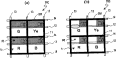
在一般的LCD中,如图21所示,像素是矩形状。与此相对,本实施方式中的LCD100的像素分别具有L字形的形状,以在列方向邻接的2个像素彼此相互啮合的方式配置。即,各像素包括具有与邻接的像素啮合那样的形状的部分(本申请说明书中称为「啮合部」。)。而且,各像素的反射区域Rf配置在各像素的啮合部中。In a general LCD, pixels are rectangular as shown in FIG. 21 . On the other hand, the pixels of
在本实施方式中,红像素R的啮合部与绿像素G的啮合部相互啮合,蓝像素B的啮合部与黄像素Ye的啮合部相互啮合。红像素R的啮合部、绿像素G的啮合部、蓝像素B的啮合部以及黄像素Ye的啮合部配置成沿着行方向带状地连续,红像素R的反射区域Rf、绿像素G的反射区域Rf、蓝像素B的反射区域Rf以及黄像素Ye的反射区域Rf也带状地连续。In this embodiment, the meshing portion of the red pixel R meshes with the meshing portion of the green pixel G, and the meshing portion of the blue pixel B meshes with the meshing portion of the yellow pixel Ye. The meshing portion of the red pixel R, the meshing portion of the green pixel G, the meshing portion of the blue pixel B, and the meshing portion of the yellow pixel Ye are arranged continuously in a strip along the row direction, and the reflection region Rf of the red pixel R and the green pixel G The reflective region Rf, the reflective region Rf of the blue pixel B, and the reflective region Rf of the yellow pixel Ye are also continuous in a strip shape.
在LCD100中,如上所述,各像素包括具有与邻接的像素啮合那样形状的啮合部,各像素的反射区域配置在该啮合部中。通过做成这样的结构,在保持了高开口率的状态下,能够实现使透过模式优先的显示。以下,说明其理由。In
图2(a)表示比较例的LCD700。比较例的LCD700虽然有红像素R、绿像素G、蓝像素B以及黄像素Ye,但是LCD700的各像素是矩形状,没有啮合部。FIG. 2( a ) shows an
在LCD700中,在重视透过模式的显示时,需要缩小反射区域Rf的面积,增大透过区域Tr的面积。然而,为了保持高开口率,需要在反射区域Rf内配置配线或者TFT11,由于配线间的间隔或者TFT11的大小存在制约,因此不能无限制地减小反射区域Rf的面积。In the
例如,如图2(b)所示,如果通过减小沿着反射区域Rf的行方向(扫描配线12延伸的方向)的宽度,强行减小反射区域Rf的面积,则在反射区域Rf内不能配置横切像素内的扫描配线12的一部分(图中用虚线包围表示),该开口率降低。For example, as shown in FIG. 2(b), if the area of the reflective region Rf is forcibly reduced by reducing the width along the row direction of the reflective region Rf (the direction in which the
与此相对,如图1所示的本实施方式中的LCD100那样,设置具有与各像素邻接的像素啮合那样形状的啮合部,如果在该啮合部中配置反射区域Rf,则在反射区域Rf内收容了横切像素内的配线或者TFT11的状态下,能够充分减小反射区域Rf。因此,能够充分增大透过区域Tr的面积,能够充分提高室内的显示品质。On the other hand, as in the
另外,在图2(b)所示的结构中,由于反射区域Rf岛状地散布,因此在形成用于形成多间隙结构的透明电介质层时,需要在行方向和列方向的双方考虑调整余量。与此相对,在本实施方式的LCD100中,在啮合部中设置有反射区域Rf的结果,反射区域Rf由于配置成带状地连续,因此只要将电介质层也形成为带状地连续即可,对于连续的方向不需要考虑调整余量。因此,能提高对反射区域Rf的开口率(反射开口率)。In addition, in the structure shown in FIG. 2(b), since the reflective regions Rf are scattered in an island shape, when forming the transparent dielectric layer for forming the multi-gap structure, it is necessary to consider adjustment margins in both the row direction and the column direction. quantity. On the other hand, in the
进而,本实施方式的LCD100在透过模式的显示和反射面模式的显示的双方中都能实现适当的白平衡这一点也很出色。以下说明其理由。Furthermore, the
在以红、绿以及蓝上加入了黄的4原色进行显示的情况下,白平衡易于破坏,有时所显示的白色带有一些黄色(即,白色的色温度降低)。关于透过模式的显示,通过调整背光的光源(具体地讲使用产生带有一些蓝色的白色光的光源)能够实现最佳的白平衡,而在反射模式下由于使用周围光进行显示,因此不能这样调整白平衡。In the case of displaying the four primary colors of red, green, and blue with yellow added, the white balance tends to be disrupted, and sometimes the displayed white may be slightly yellowed (that is, the color temperature of white is lowered). Regarding the display in the transmissive mode, the best white balance can be achieved by adjusting the light source of the backlight (specifically, using a light source that produces white light with some bluishness), while in the reflective mode, since the display uses ambient light, the The white balance cannot be adjusted in this way.
因此,考虑通过调整反射区域Rf的面积来调整反射显示的白平衡。具体地讲,通过使蓝像素B的反射区域Rf的面积比黄像素Ye的反射区域Rf的面积大,能够防止反射模式的白色带有黄色。Therefore, it is considered to adjust the white balance of the reflective display by adjusting the area of the reflective region Rf. Specifically, by making the area of the reflective region Rf of the blue pixel B larger than the area of the reflective region Rf of the yellow pixel Ye, it is possible to prevent white in the reflective mode from being yellowish.
然而,如果这样调整白平衡,则发生新的问题。例如,在图2(b)所示的比较例的LCD700中,如果增大蓝像素B的反射区域Rf的面积并减小黄像素Ye的反射区域Rf的面积,则如图3所示,由于蓝像素B的透过区域Tr的面积比黄像素Ye的透过区域Tr的面积小,因此透过模式的白色带有黄色。为了防止这一点,还考虑把照明装置的光源进一步改变成发出带有蓝色的强光的光源,但由于使光源的光的蓝色增强,降低背光的亮度。However, if the white balance is adjusted in this way, a new problem occurs. For example, in the
与此相对,在本实施方式的LCD100中,由于显示存在相互补色关系的颜色的2个像素的啮合部,即,蓝像素B的啮合部与黄像素Te的啮合部相互啮合,因此通过调整这些啮合部的面积,如图4所示,能够不改变蓝像素B的透过区域Tr与黄像素Ye的透过区域Tr的面积比,而改变蓝像素B的反射区域Rf与黄像素Ye的反射区域Rf的面积比(具体地讲,使蓝像素B的反射区域Rf的面积比黄像素Ye的反射区域Rf的面积大)。因此,能够不破坏透过显示的白平衡,就调整反射显示的白平衡,能够实现在透过模式的显示和反射面模式的显示的双方中都优选的白平衡。On the other hand, in the
表1以及图5中表示通过改变反射区域Rf的面积来调整反射模式的显示的白平衡的例子(实施例1~5)。表1显示红像素R、绿像素G、蓝像素B以及黄像素Ye的反射区域Rf的面积与在反射模式下显示的白色的色温度以及xy色度的关系。另外,图5是描绘了在实施例1~5中在反射模式下显示的白色的xy色度图。另外,这里表示的数据是关于在反射显示中使用表示图6所示的分光特性的彩色滤光片、在透过光强度中表示图7所示的波长依赖性的液晶层、具有图8表示的光谱的外光(周围光)的LCD的数据。Table 1 and FIG. 5 show examples (Examples 1 to 5) of adjusting the white balance of the reflective mode display by changing the area of the reflective region Rf. Table 1 shows the relationship between the area of the reflective region Rf of the red pixel R, the green pixel G, the blue pixel B and the yellow pixel Ye and the color temperature and xy chromaticity of white displayed in the reflective mode. In addition, FIG. 5 is an xy chromaticity diagram depicting white color displayed in reflection mode in Examples 1 to 5. FIG. In addition, the data shown here are about using a color filter showing the spectral characteristics shown in FIG. 6 in reflective display, and showing the wavelength dependence of transmitted light intensity shown in FIG. The spectrum of the external light (ambient light) of the LCD data.
[表1][Table 1]
如表1以及图5所示,在实施例1中,由于红像素R、绿像素G、蓝像素B以及黄像素Ye的反射区域Rf的面积相互相等,因此白色的色温度低,白色带有一些黄色。与此相对,在实施例2、3以及4中,由于蓝像素B的反射区域Rf的面积比黄像素Ye的反射区域Rf的面积大,因此能够提高白色的色温度。另外,如将实施例2、3以及4相互进行比较所知那样,对于黄像素Ye的反射区域Rf的面积,越增大蓝像素B的反射区域Rf的面积,白色的色温度越高。另外,如将实施例3与实施例5进行比较所知那样,不仅能够使蓝像素B的反射区域Rf的面积比黄像素Ye的反射区域Rf的面积大,而且通过减少红像素R的反射区域Rf的面积,能够进一步提高白色的色温度。As shown in Table 1 and FIG. 5, in Embodiment 1, since the areas of the reflection regions Rf of the red pixel R, the green pixel G, the blue pixel B, and the yellow pixel Ye are equal to each other, the color temperature of white is low, and the white color some yellow. In contrast, in Examples 2, 3, and 4, since the area of the reflection region Rf of the blue pixel B is larger than the area of the reflection region Rf of the yellow pixel Ye, the color temperature of white can be increased. Also, as is known from comparing Examples 2, 3, and 4, the larger the area of the reflection region Rf of the blue pixel B with respect to the area of the reflection region Rf of the yellow pixel Ye, the higher the color temperature of white. In addition, as is known from a comparison between Example 3 and Example 5, not only can the area of the reflection region Rf of the blue pixel B be larger than the area of the reflection region Rf of the yellow pixel Ye, but also by reducing the area of the reflection region Rf of the red pixel R The area of Rf can further increase the color temperature of white.
另外,在本实施方式中,如图9(a)所示,例示了各像素的啮合部与属于同一个图像元素的像素啮合的情况,但本发明并不限于这种情况。如图9(b)所示,也可以是各像素的啮合部与属于不同图像元素的像素啮合那样的结构。In addition, in this embodiment, as shown in FIG. 9( a ), a case where the meshing portion of each pixel meshes with a pixel belonging to the same picture element is exemplified, but the present invention is not limited to this case. As shown in FIG. 9( b ), a structure may be adopted in which the meshing portion of each pixel meshes with pixels belonging to different picture elements.
在图9(b)表示的结构中,各像素具有L字形的形状,具有啮合部的,但各像素的啮合部不是与属于相同图像元素的像素,而是与属于不同图像元素的像素啮合。具体地讲,如果着眼于某个图像元素,则红像素R的啮合部与属于下一个图像元素的绿像素G啮合,绿像素G的啮合部与属于上一个图像元素的红像素R啮合。另外,蓝像素B的啮合部与属于下一个图像元素的黄像素Ye啮合,黄像素Ye的啮合部与属于上一个图像元素的蓝像素B啮合。即使采用这种结构,也同样能够得到上述的效果。In the structure shown in FIG. 9( b ), each pixel has an L-shaped shape and has an engaging portion, but the engaging portion of each pixel is not engaged with a pixel belonging to the same image element, but is engaged with a pixel belonging to a different image element. Specifically, when focusing on a certain image element, the meshing portion of the red pixel R meshes with the green pixel G belonging to the next image element, and the meshing portion of the green pixel G meshes with the red pixel R belonging to the previous image element. In addition, the meshing portion of the blue pixel B meshes with the yellow pixel Ye belonging to the next picture element, and the meshing portion of the yellow pixel Ye meshes with the blue pixel B belonging to the previous picture element. Even with such a configuration, the above-mentioned effects can be obtained in the same manner.
另外,如果配置成使各像素的啮合部与属于不同图像元素的像素啮合,则当在黑底上显示白色的线时,与线的延伸方向无关,能够进行适当的显示。Also, if the meshing portion of each pixel is arranged to mesh with pixels belonging to different picture elements, when a white line is displayed on a black matrix, appropriate display can be performed regardless of the direction in which the line extends.
如图9(a)所示,如果配置成使各像素的啮合部与属于同一个图像元素的像素啮合,则在1个图像元素内反射区域Rf配置成在行方向带状地连续。因此,如果在黑底上显示白色的线,则如图10(a)所示,在沿着行方向延伸的线与沿着列方向延伸的线之间,在粗细方面产生很大的差异。As shown in FIG. 9( a ), if the meshing portion of each pixel is arranged to mesh with a pixel belonging to the same picture element, the reflective region Rf is arranged continuously in a strip in the row direction within one picture element. Therefore, when white lines are displayed on a black matrix, as shown in FIG. 10( a ), there is a large difference in thickness between the lines extending in the row direction and the lines extending in the column direction.
与此相对,如图9(b)所示,如果配置成使得各像素的啮合部与属于不同图像元素的像素啮合,则在1个图像元素内反射区域Rf以相对于图像元素的中心大致均等的距离配置。因此,如果在黑底上显示白色的钱,则如图10(b)所示,沿着行方向延伸的线与沿着列方向延伸的线的粗细大致相同,不论线的延伸方向,能够进行适当的显示。On the other hand, as shown in FIG. 9( b ), if the meshing portion of each pixel is arranged such that the pixel belonging to a different picture element meshes, the reflective area Rf in one picture element is approximately equal to the center of the picture element. distance configuration. Therefore, if white money is displayed on a black background, as shown in FIG. Appropriate display.
其次,说明本实施方式中的LCD100的更具体的结构。图11是表示LCD100的具体结构的一个例子的上面图,图12是沿着图11中的12A-12A’线的截面图。另外,图11中,为了易于观看,省略了各像素的反射区域Rf的阴影线。Next, a more specific structure of
LCD100具备具有设置在多个像素的每一个上的TFT11的有源矩阵基板(以下称为「TFT基板」。)100a、与TFT基板100a相对的彩色滤光片基板100b、以及配置在它们之间的液晶层40。The
TFT基板100a具有在透明的绝缘性基板(例如玻璃基板)10上叠层了多个膜的结构。以下,更具体地说明TFT基板100a的结构。The
首先,以覆盖绝缘性基板10的大致整个面的方式形成底涂膜15。在该底涂膜15上,设置有构成TFT11的半导体层16、用于构成辅助电容的辅助电容电极17、和将半导体层16与辅助电容电极17电连接的辅助电容连接配线18。半导体层16、辅助电容电极17以及辅助电容连接配线18由同一个半导体膜形成。First,
形成栅极绝缘膜19,使得覆盖这些半导体层16、辅助电容电极17以及辅助电容连接配线18。在栅极绝缘膜19上,设置有扫描配线12以及辅助电容配线14、从扫描配线12延伸设置的栅极电极20。辅助电容配线14隔着栅极绝缘膜19与辅助电容电极17相对,由辅助电容配线14和辅助电容电极17以及位于它们之间的栅极绝缘膜19形成辅助电容Cs。在图11中,将红像素R用、绿像素G用、蓝像素B用、黄像素Ye用的辅助电容分别表示为Cs(R)、Cs(G)、Cs(B)、Cs(Ye)。The
形成第一层间绝缘膜(例如无机绝缘膜)21,使得覆盖扫描配线12等。在第一层间绝缘膜21上,形成有信号配线13、源极电极22以及漏极电极23。源极电极22以及漏极电极23在形成于栅极绝缘膜19以及第一层间绝缘膜21上的接触孔CH中与半导体层16连接。A first interlayer insulating film (for example, an inorganic insulating film) 21 is formed so as to cover the
形成第二层间绝缘膜(例如透明树脂膜)24,使得覆盖信号配线13。在该第二层间绝缘膜24上,形成有包括透明电极25a以及反射电极25b的像素电极25。像素电极25在形成于第二层间绝缘膜24的接触孔CH中与漏极电极23连接。形成取向膜26使得覆盖像素电极25。A second interlayer insulating film (for example, a transparent resin film) 24 is formed so as to cover the
彩色滤光片基板100b具有透明的绝缘性基板(例如玻璃基板)30、形成在绝缘性基板30上的红彩色滤光片31R、绿彩色滤光片31G、蓝彩色滤光片31B、黄彩色滤光片31Ye以及黑点矩阵BM。在这些彩色滤光片以及黑点矩阵形BM上,仅在反射区域Rf中选择性地形成透明电介质层(例如透明树脂层)32。而且,设置相对电极33以及取向膜34,使得覆盖透明电介质层32。The
作为液晶层40,能够使用各种显示模式用的液晶层。由在反射区域Rf上选择性地形成的透明电介质层32在彩色滤光片基板100b上形成台阶差,由此,反射区域Rf中的液晶层40的厚度与透过区域Tr中的液晶层40的厚度不同。As the
在图11以及图12中例示了结构的LCD100能够使用众所周知的各种制造方法进行制造。The
另外,在图11中,表示4个像素和2条扫描配线12,位于上侧的2个像素(具体地讲是绿像素G以及黄像素Ye)的TFT11与下侧的扫描配线12连接,而位于下侧的2个像素(具体地讲是红像素R以及蓝像素B)的TFT11与上侧的扫描配线12连接。In addition, in FIG. 11 , four pixels and two scanning
与此相对,也可以如图13所示,在上侧的扫描配线12上连接位于上侧的绿像素G以及黄像素Ye的TFT11,在下侧的扫描配线12上连接位于下侧的红像素R以及蓝像素B的TFT11。On the other hand, as shown in FIG. 13 , the green pixel G and the
其中,无论采用哪一种结构,各像素的辅助电容连接配线18都如图11或者图13所示,优选配置成不是跨过驱动该像素的扫描配线12,而是跨过驱动邻接像素的扫描配线12。例如,如果着眼于图11表示的红像素R进行说明,则该红像素R的辅助电容连接配线18配置成不是跨过驱动红像素R的扫描配线12(图中上侧的扫描配线),而是跨过驱动绿像素G的扫描配线12(图中下侧的扫描配线)。Wherein, no matter which structure is adopted, the auxiliary
在辅助电容连接配线18与扫描配线12交叉的部分中形成寄生电容。在各像素的辅助电容连接配线18跨过驱动其像素的扫描配线12的情况下,所形成的寄生电容成为在栅极关断时产生的引入电位的原因,对最佳的相对电极电位产生影响。因此,各像素的辅助电容连接配线18优选配置成跨过驱动邻接像素的扫描配线12。A parasitic capacitance is formed in a portion where the auxiliary
另外,在图13表示的结构中,为了以跨过驱动邻接像素的扫描配线12的方式配置各像素的辅助电容连接配线18,在邻接的像素内形成辅助电容。具体地讲,在绿像素G内形成红像素R用的辅助电容Cs(R),在黄像素Ye内形成蓝像素B用的辅助电容Cs(B)。另外,在红像素R内形成绿像素G用的辅助电容Cs(G),在蓝像素B内形成黄像素Ye用的辅助电容Cs(Ye)。In the configuration shown in FIG. 13 , storage
如图13所示,如果辅助电容连接配线18横切其它像素内,则在像素之间形成电容。因此,在进行了信号向像素的写入以后,在邻接像素的电位变动的影响下受到引入,电压透过率特性移动。因此,在上述的2个像素(绿像素G以及黄像素Ye)与下侧的2个像素(红像素R以及蓝像素B)中,在电压透过率特性方面产生差异。As shown in FIG. 13 , when the auxiliary
对于这样的问题,通过在红像素R、绿像素G、蓝像素B以及黄像素Ye的每一个中独立地设计γ,能够进行改善。Such a problem can be improved by independently designing γ in each of the red pixel R, the green pixel G, the blue pixel B, and the yellow pixel Ye.
另外,即使是图11所示的结构,有时对于各像素,像素间电容分散,在电压透过率特性方面产生差异,而即使是这样的情况,也可以在红像素R、绿像素G、蓝像素B以及黄像素Ye的每一个中独立地设定γ。In addition, even with the structure shown in FIG. 11 , there may be differences in the voltage transmittance characteristics due to the dispersion of capacitance between pixels for each pixel, but even in such a case, red pixel R, green pixel G, blue pixel γ is set independently for each of the pixel B and the yellow pixel Ye.
另外,在到此为止的说明中,例示了带状地配置的啮合部如图1等所示,按照红像素R的啮合部、绿像素G的啮合部、蓝像素B的啮合部、黄像素Ye的啮合部的顺序连续,在各像素内反射区域Rf按照红、绿、蓝、黄的顺序连续的情况,而啮合部以及反射区域Rf的顺序并不限于这种情况。In addition, in the description up to this point, the meshing parts arranged in a strip shape have been exemplified, as shown in FIG. The order of the meshing parts of Ye is continuous, and the reflective regions Rf are continuous in the order of red, green, blue, and yellow in each pixel, but the order of the meshing parts and the reflective regions Rf is not limited to this case.
例如,如图14(a)以及(b)所示,也可以按照红像素R的啮合部、绿像素G的啮合部、黄像素Ye的啮合部、蓝像素B的啮合部的顺序连续,各像素内反射区域Rf也可以按照红、绿、黄、蓝的顺序连续。For example, as shown in Fig. 14 (a) and (b), it is also possible to follow the sequence of the meshing portion of the red pixel R, the meshing portion of the green pixel G, the meshing portion of the yellow pixel Ye, and the meshing portion of the blue pixel B, each The reflective regions Rf in the pixels may also be continuous in the order of red, green, yellow, and blue.
一般地,在红像素R、绿像素G、蓝像素B以及黄像素Ye之中,红像素R以及蓝像素B的亮度相对低,绿像素G以及黄像素Ye的亮度相对高。因此,如果在像素内反射区域Rf按照红、绿、蓝、黄的顺序连续,则如在图15(a)中模式地表示的那样,由于交叉配置亮度低的反射区域Rf和亮度高的反射区域Rf,因此在显示全图像时能够进行均匀的显示。Generally, among the red pixel R, the green pixel G, the blue pixel B and the yellow pixel Ye, the brightness of the red pixel R and the blue pixel B is relatively low, and the brightness of the green pixel G and the yellow pixel Ye is relatively high. Therefore, if the reflective regions Rf in the pixel are continuous in the order of red, green, blue, and yellow, as shown schematically in FIG. The region Rf, therefore, can be displayed uniformly when displaying a full image.
另一方面,如果在像素内反射区域Rf按照红、绿、黄、蓝的顺序连接,则如在图15(b)中模式的表示的那样,由于亮度高的反射区域配置在像素的中央,所以在黑底上显示白色的线或者在白地上显示黑色的线时,能够防止线边缘带色。On the other hand, if the reflective regions Rf are connected in the order of red, green, yellow, and blue in the pixel, as shown schematically in FIG. Therefore, when displaying a white line on a black ground or a black line on a white ground, it is possible to prevent the edge of the line from being colored.
另外,也可以将啮合部配置成按照绿像素G的啮合部、红像素R的啮合部、黄像素Ye的啮合部、蓝像素B的啮合部的顺序连续。如果这样配置,则在像素内反射区域Rf按照绿、红、黄、蓝的顺序连续。因此,如在图15(c)中模式地表示的那样,由于亮度低的反射区域Rf与亮度高的反射区域Rf交互配置,因此在这种情况下,也可以得到能够均匀地显示全图像这样的效果。In addition, the meshing portions may be arranged continuously in the order of the meshing portion of the green pixel G, the meshing portion of the red pixel R, the meshing portion of the yellow pixel Ye, and the meshing portion of the blue pixel B. If arranged in this way, the reflective regions Rf are continuous in the order of green, red, yellow, and blue in the pixel. Therefore, as shown schematically in FIG. 15(c), since the reflective regions Rf with low luminance and the reflective regions Rf with high luminance are arranged alternately, even in this case, it is also possible to obtain a display in which the entire image can be uniformly displayed. Effect.
(实施方式2)(Embodiment 2)
参照图16以及图17,说明本实施方式中的LCD200。图16是模式地表示LCD200的上面图,图17是沿着图16中的17A-17A’线的截面图。以下,以与实施方式1中的LCD100不同的点为中心进行说明。
本实施方式中的LCD200是在CPA(Continuous PinwheelAlignment:连续焰火状排列)模式下进行显示的LCD。在CPA模式下,在隔着垂直取向型的液晶层相对的一对电极的一个中设置开口部以及切口部,通过使用在这些开口部或者切口部的边缘部中生成的倾斜电场,使液晶分子放射状地倾斜取向,由此实现在广视野角下的高品质的显示。例如在特开2003-43525号公报或者特开2002-202511号公报中公开了CPA模式。The
在LCD200的TFT基板200a上设置的像素电极25中,形成开口部以及/或者切口部(均没有图示)。如果在像素电极25与相对电极33之间施加电压,则在开口部或者切口部的边缘部形成倾斜电场。液晶层40的液晶分子由该倾斜电场控制在电压施加时倒下的方向。因此,在液晶层40中,形成液晶分子放射状地倾斜取向的多个区域。所生成的各个区域称为液晶畴(domain)。In
在本实施方式中,进而在相对基板200b上形成用于使液晶畴的取向稳定的突起(铆钉)35。突起35形成在与电压施加时所形成的液晶畴的大致中央相对应的位置上。突起35例如由透明的树脂形成。In this embodiment, protrusions (rivets) 35 for stabilizing the alignment of liquid crystal domains are further formed on the counter substrate 200b. The
在图11所示的LCD100中,从辅助电容电极17延伸的辅助电容连接配线18直接连接到半导体层16上,辅助电容连接配线18从辅助电容电极17延伸至半导体层16,使得横切像素内。In the
与此相对,在本实施方式中,辅助电容连接配线18通过由与源极电极22或者漏极电极23相同的导电膜形成的导电部件27、像素电极25、漏极电极23,与半导体层16连接。辅助电容连接配线18在形成于与突起35重叠的位置的接触孔CH中,在导电部件27上形成,导电部件27同样地在形成于与突起35重叠的位置的接触孔CH中,与像素电极25连接。On the other hand, in the present embodiment, the storage
辅助电容连接配线18由于由半导体膜形成,因此光透过率低(例如50%左右)。在本实施方式中,由于仅需要把辅助电容连接配线18延伸到与突起35重叠的位置,因此能够降低以辅助电容连接配线18为起因的光透过率的下降,能够实现更明亮的显示。另外,与突起35重叠的区域的液晶层,由于原本对显示没有多少贡献(光透过率低),因此在该区域中即使设置接触孔,透过率的降低也不构成问题。Since the storage
在上述的实施方式1以及2中,以使用4色以上的原色进行显示的多原色LCD为例说明了本发明,但本发明并不限于多原色LCD,能够广泛用在1个图像元素由4个以上像素规定的透过反射两用型LCD中。In
例如,由在显示红的红像素、显示绿的绿像素以及显示蓝的蓝像素中,加入了显示白色的白像素的4个像素规定1个图像元素的LCD中也可以使用本发明。如果在显示三原色的3个像素中加入显示白色的白像素,则能够提高各图像元素的亮度,实现更明亮的显示。For example, the present invention can also be used in an LCD in which one picture element is defined by four pixels including a red pixel that displays red, a green pixel that displays green, and a blue pixel that displays blue, plus a white pixel that displays white. If a white pixel that displays white is added to the three pixels that display the three primary colors, the brightness of each image element can be increased to achieve a brighter display.
产业上的可利用性Industrial availability
依据本发明,在1个图像元素由4个以上像素规定的透过反射两用型液晶显示装置中,能够实现开口率高而且在重视了透过模式的显示中优选的结构。According to the present invention, in a transflective liquid crystal display device in which one picture element is defined by four or more pixels, it is possible to realize a structure that has a high aperture ratio and is preferable for a transmissive mode display.
本发明能够适当地使用在1个图像元素由4个以上像素规定的透过反射两用型液晶显示装置中,特别是,能够适当地使用在用4色以上的原色进行显示的多原色液晶显示装置中。The present invention can be suitably used in a transflective liquid crystal display device in which one picture element is defined by four or more pixels, and in particular, can be suitably used in a multi-primary-color liquid crystal display for displaying with four or more primary colors. device.
Claims (14)
Applications Claiming Priority (3)
| Application Number | Priority Date | Filing Date | Title |
|---|---|---|---|
| JP2006075083 | 2006-03-17 | ||
| JP075083/2006 | 2006-03-17 | ||
| PCT/JP2007/052962 WO2007119288A1 (en) | 2006-03-17 | 2007-02-19 | Liquid crystal display device |
Publications (2)
| Publication Number | Publication Date |
|---|---|
| CN101405648A true CN101405648A (en) | 2009-04-08 |
| CN101405648B CN101405648B (en) | 2011-12-07 |
Family
ID=38609106
Family Applications (1)
| Application Number | Title | Priority Date | Filing Date |
|---|---|---|---|
| CN2007800094469A Expired - Fee Related CN101405648B (en) | 2006-03-17 | 2007-02-19 | Liquid crystal display device |
Country Status (4)
| Country | Link |
|---|---|
| US (2) | US7880834B2 (en) |
| JP (1) | JP4994366B2 (en) |
| CN (1) | CN101405648B (en) |
| WO (1) | WO2007119288A1 (en) |
Cited By (7)
| Publication number | Priority date | Publication date | Assignee | Title |
|---|---|---|---|---|
| CN102062971A (en) * | 2010-11-26 | 2011-05-18 | 友达光电股份有限公司 | Liquid crystal display device, liquid crystal display panel and color filter substrate thereof |
| CN102854555A (en) * | 2011-07-01 | 2013-01-02 | 元太科技工业股份有限公司 | Color filter and color display device using the same |
| WO2013037236A1 (en) * | 2011-09-16 | 2013-03-21 | 上海天马微电子有限公司 | Array substrate and liquid crystal display panel |
| CN103033974A (en) * | 2011-09-30 | 2013-04-10 | 乐金显示有限公司 | Liquid crystal display device |
| WO2014121574A1 (en) * | 2013-02-05 | 2014-08-14 | 北京京东方光电科技有限公司 | Array substrate and liquid crystal display panel |
| CN107077034A (en) * | 2014-09-12 | 2017-08-18 | 夏普株式会社 | Display device |
| CN109686263A (en) * | 2019-01-15 | 2019-04-26 | 云谷(固安)科技有限公司 | A pixel structure, a display panel and a display device |
Families Citing this family (11)
| Publication number | Priority date | Publication date | Assignee | Title |
|---|---|---|---|---|
| JP5339972B2 (en) * | 2009-03-10 | 2013-11-13 | 株式会社ジャパンディスプレイ | Image display device |
| JP2011128265A (en) * | 2009-12-16 | 2011-06-30 | Mitsubishi Electric Corp | Display device |
| KR101664225B1 (en) * | 2009-12-21 | 2016-10-10 | 엘지디스플레이 주식회사 | Liquid Crystal Display Device |
| US8902373B2 (en) * | 2010-03-04 | 2014-12-02 | Sharp Kabushiki Kaisha | Liquid crystal display device |
| WO2012005022A1 (en) * | 2010-07-09 | 2012-01-12 | シャープ株式会社 | Liquid crystal display device |
| WO2012077565A1 (en) * | 2010-12-08 | 2012-06-14 | シャープ株式会社 | Liquid crystal display device |
| JP6195696B2 (en) * | 2012-05-17 | 2017-09-13 | シャープ株式会社 | Liquid crystal display |
| CN103048838B (en) * | 2012-12-13 | 2015-04-15 | 北京京东方光电科技有限公司 | Array substrate, liquid crystal display panel and driving method |
| US20200174312A1 (en) * | 2017-05-25 | 2020-06-04 | Sharp Kabushiki Kaisha | Display device |
| US10642090B2 (en) * | 2017-08-17 | 2020-05-05 | Mitsubishi Electric Corporation | Liquid crystal display device |
| JP2019090916A (en) * | 2017-11-14 | 2019-06-13 | 株式会社ジャパンディスプレイ | Display device |
Family Cites Families (16)
| Publication number | Priority date | Publication date | Assignee | Title |
|---|---|---|---|---|
| US4800375A (en) * | 1986-10-24 | 1989-01-24 | Honeywell Inc. | Four color repetitive sequence matrix array for flat panel displays |
| JP3362758B2 (en) | 1996-03-15 | 2003-01-07 | 富士ゼロックス株式会社 | Reflective color display |
| US6195140B1 (en) * | 1997-07-28 | 2001-02-27 | Sharp Kabushiki Kaisha | Liquid crystal display in which at least one pixel includes both a transmissive region and a reflective region |
| JP4034022B2 (en) | 2000-01-25 | 2008-01-16 | シャープ株式会社 | Liquid crystal display |
| JP2001306023A (en) | 2000-04-18 | 2001-11-02 | Seiko Epson Corp | Image display device |
| JP3712637B2 (en) * | 2000-08-11 | 2005-11-02 | シャープ株式会社 | Liquid crystal display device and defect correcting method thereof |
| JP3601788B2 (en) * | 2000-10-31 | 2004-12-15 | シャープ株式会社 | Liquid crystal display |
| AU2002304276A1 (en) * | 2001-06-11 | 2002-12-23 | Moshe Ben-Chorin | Device, system and method for color display |
| EP1497820A4 (en) * | 2002-04-11 | 2009-03-11 | Genoa Color Technologies Ltd | COLOR DISPLAY DEVICES AND METHODS HAVING IMPROVED ATTRIBUTES |
| JP4092177B2 (en) * | 2002-10-29 | 2008-05-28 | シャープ株式会社 | Liquid crystal display |
| KR100491257B1 (en) * | 2002-12-31 | 2005-05-24 | 엘지.필립스 엘시디 주식회사 | Transreflective liquid crystal display device |
| US7136124B2 (en) * | 2003-05-30 | 2006-11-14 | Innolux Display Corp. | Transflective liquid crystal display device using transflective color filter and method for making color filter |
| TWI285288B (en) * | 2004-04-27 | 2007-08-11 | Au Optronics Corp | Liquid crystal panel and liquid crystal display |
| JP4328738B2 (en) * | 2004-05-06 | 2009-09-09 | キヤノン株式会社 | LCD color display |
| KR101041970B1 (en) * | 2004-06-11 | 2011-06-16 | 삼성전자주식회사 | Liquid crystal display |
| JP2006058332A (en) * | 2004-08-17 | 2006-03-02 | Seiko Epson Corp | Electro-optical device and electronic apparatus |
-
2007
- 2007-02-19 US US12/293,221 patent/US7880834B2/en active Active
- 2007-02-19 CN CN2007800094469A patent/CN101405648B/en not_active Expired - Fee Related
- 2007-02-19 JP JP2008510744A patent/JP4994366B2/en not_active Expired - Fee Related
- 2007-02-19 WO PCT/JP2007/052962 patent/WO2007119288A1/en not_active Ceased
-
2010
- 2010-12-16 US US12/970,022 patent/US8289480B2/en not_active Expired - Fee Related
Cited By (15)
| Publication number | Priority date | Publication date | Assignee | Title |
|---|---|---|---|---|
| TWI406017B (en) * | 2010-11-26 | 2013-08-21 | Au Optronics Corp | Lcd apparatus, lcd panel, and color filter substrate thereof |
| CN102062971B (en) * | 2010-11-26 | 2012-01-25 | 友达光电股份有限公司 | Liquid crystal display device, liquid crystal display panel and color filter substrate thereof |
| CN102062971A (en) * | 2010-11-26 | 2011-05-18 | 友达光电股份有限公司 | Liquid crystal display device, liquid crystal display panel and color filter substrate thereof |
| CN102854555A (en) * | 2011-07-01 | 2013-01-02 | 元太科技工业股份有限公司 | Color filter and color display device using the same |
| US8934184B2 (en) | 2011-07-01 | 2015-01-13 | E Ink Holdings Inc. | Color filter and color display device using same |
| WO2013037236A1 (en) * | 2011-09-16 | 2013-03-21 | 上海天马微电子有限公司 | Array substrate and liquid crystal display panel |
| CN102998862A (en) * | 2011-09-16 | 2013-03-27 | 上海天马微电子有限公司 | Array substrate and liquid crystal display panel |
| US9436043B2 (en) | 2011-09-16 | 2016-09-06 | Shanghai Tianma Micro-electronics Co., Ltd. | Array substrate and liquid crystal display panel |
| CN103033974A (en) * | 2011-09-30 | 2013-04-10 | 乐金显示有限公司 | Liquid crystal display device |
| CN103033974B (en) * | 2011-09-30 | 2015-12-16 | 乐金显示有限公司 | Liquid crystal display device |
| WO2014121574A1 (en) * | 2013-02-05 | 2014-08-14 | 北京京东方光电科技有限公司 | Array substrate and liquid crystal display panel |
| CN107077034A (en) * | 2014-09-12 | 2017-08-18 | 夏普株式会社 | Display device |
| CN107077034B (en) * | 2014-09-12 | 2020-11-17 | 夏普株式会社 | Display device |
| CN109686263A (en) * | 2019-01-15 | 2019-04-26 | 云谷(固安)科技有限公司 | A pixel structure, a display panel and a display device |
| CN109686263B (en) * | 2019-01-15 | 2022-05-03 | 云谷(固安)科技有限公司 | Pixel structure, display panel and display device |
Also Published As
| Publication number | Publication date |
|---|---|
| US20110085101A1 (en) | 2011-04-14 |
| JPWO2007119288A1 (en) | 2009-08-27 |
| JP4994366B2 (en) | 2012-08-08 |
| US20090073358A1 (en) | 2009-03-19 |
| US8289480B2 (en) | 2012-10-16 |
| WO2007119288A1 (en) | 2007-10-25 |
| US7880834B2 (en) | 2011-02-01 |
| CN101405648B (en) | 2011-12-07 |
Similar Documents
| Publication | Publication Date | Title |
|---|---|---|
| CN101405648A (en) | Liquid crystal display device | |
| US7561239B2 (en) | Liquid crystal device and electronic apparatus | |
| US8305526B2 (en) | Method for providing light to liquid crystal panel | |
| US8913093B2 (en) | Liquid crystal display device | |
| US20090309821A1 (en) | Display Device | |
| US8035778B2 (en) | Display panel, electro-optical apparatus and fabricating methods thereof | |
| JP4956786B2 (en) | Image display system | |
| US7471358B2 (en) | Liquid crystal display device | |
| US10895779B2 (en) | Liquid crystal display with red, green, blue, and white subpixels having reflective and transmissive areas | |
| US10197847B2 (en) | Liquid crystal display device | |
| JP2007140089A (en) | Liquid crystal display | |
| JP2007140457A (en) | Driving circuit for electro-optical device and electronic apparatus | |
| US7728930B2 (en) | Display panel, electro-optical device, and methods for fabricating the same | |
| US8223302B2 (en) | Display panel, electro-optical apparatus, and methods for manufacturing the same | |
| US20070109453A1 (en) | Electro-optical apparatus and electronic apparatus | |
| CN100476540C (en) | Electro-optical device and electronic apparatus | |
| JP2006313358A (en) | Liquid crystal display | |
| US7580094B2 (en) | Transreflective LCD panel and electronic device using the same | |
| JP2007133059A (en) | Electro-optical device, method for manufacturing the same, and electronic apparatus | |
| JP2006350281A (en) | Electro-optical device and electronic equipment | |
| JP2008233137A (en) | Liquid crystal display device | |
| CN113721393A (en) | Pixel structure | |
| JP2007093668A (en) | Liquid crystal device and electronic equipment | |
| JP2007226084A (en) | Display device, color filter, liquid crystal display device provided with them, panel for liquid crystal display device and electronic equipment |
Legal Events
| Date | Code | Title | Description |
|---|---|---|---|
| C06 | Publication | ||
| PB01 | Publication | ||
| C10 | Entry into substantive examination | ||
| SE01 | Entry into force of request for substantive examination | ||
| C14 | Grant of patent or utility model | ||
| GR01 | Patent grant | ||
| CF01 | Termination of patent right due to non-payment of annual fee |
Granted publication date: 20111207 Termination date: 20200219 |
|
| CF01 | Termination of patent right due to non-payment of annual fee |