CN101382715A - Pixel structure, display panel and manufacturing method of photoelectric device - Google Patents
Pixel structure, display panel and manufacturing method of photoelectric device Download PDFInfo
- Publication number
- CN101382715A CN101382715A CNA2008101696999A CN200810169699A CN101382715A CN 101382715 A CN101382715 A CN 101382715A CN A2008101696999 A CNA2008101696999 A CN A2008101696999A CN 200810169699 A CN200810169699 A CN 200810169699A CN 101382715 A CN101382715 A CN 101382715A
- Authority
- CN
- China
- Prior art keywords
- layer
- manufacturing
- organic material
- patterned
- electrode
- Prior art date
- Legal status (The legal status is an assumption and is not a legal conclusion. Google has not performed a legal analysis and makes no representation as to the accuracy of the status listed.)
- Pending
Links
- 238000004519 manufacturing process Methods 0.000 title claims abstract description 55
- 239000010410 layer Substances 0.000 claims abstract description 419
- 239000011368 organic material Substances 0.000 claims abstract description 65
- 229920002120 photoresistant polymer Polymers 0.000 claims abstract description 64
- 239000011241 protective layer Substances 0.000 claims abstract description 55
- 239000000758 substrate Substances 0.000 claims abstract description 51
- 239000003990 capacitor Substances 0.000 claims abstract description 27
- 238000003860 storage Methods 0.000 claims abstract description 27
- 238000005530 etching Methods 0.000 claims abstract description 22
- 230000005693 optoelectronics Effects 0.000 claims abstract description 14
- 229910052751 metal Inorganic materials 0.000 claims description 95
- 239000002184 metal Substances 0.000 claims description 95
- 238000000034 method Methods 0.000 claims description 69
- 239000004065 semiconductor Substances 0.000 claims description 12
- 238000004380 ashing Methods 0.000 claims description 4
- 238000002161 passivation Methods 0.000 abstract description 3
- 239000000463 material Substances 0.000 description 43
- 229910021417 amorphous silicon Inorganic materials 0.000 description 15
- 239000010409 thin film Substances 0.000 description 10
- 239000002356 single layer Substances 0.000 description 9
- 238000001039 wet etching Methods 0.000 description 7
- ZOKXTWBITQBERF-UHFFFAOYSA-N Molybdenum Chemical compound [Mo] ZOKXTWBITQBERF-UHFFFAOYSA-N 0.000 description 6
- 238000013461 design Methods 0.000 description 6
- 238000001312 dry etching Methods 0.000 description 6
- 239000004973 liquid crystal related substance Substances 0.000 description 6
- 150000002739 metals Chemical class 0.000 description 6
- 229910052750 molybdenum Inorganic materials 0.000 description 6
- 239000011733 molybdenum Substances 0.000 description 6
- 238000000206 photolithography Methods 0.000 description 6
- 229910052782 aluminium Inorganic materials 0.000 description 5
- XAGFODPZIPBFFR-UHFFFAOYSA-N aluminium Chemical compound [Al] XAGFODPZIPBFFR-UHFFFAOYSA-N 0.000 description 5
- 229920000728 polyester Polymers 0.000 description 5
- RTAQQCXQSZGOHL-UHFFFAOYSA-N Titanium Chemical compound [Ti] RTAQQCXQSZGOHL-UHFFFAOYSA-N 0.000 description 4
- 238000010586 diagram Methods 0.000 description 4
- 238000011065 in-situ storage Methods 0.000 description 4
- 239000007769 metal material Substances 0.000 description 4
- -1 polyphenylenes Polymers 0.000 description 4
- 230000001681 protective effect Effects 0.000 description 4
- 229910052709 silver Inorganic materials 0.000 description 4
- 239000004332 silver Substances 0.000 description 4
- 229910052719 titanium Inorganic materials 0.000 description 4
- 239000010936 titanium Substances 0.000 description 4
- 229920003171 Poly (ethylene oxide) Polymers 0.000 description 3
- 239000004952 Polyamide Substances 0.000 description 3
- 239000004642 Polyimide Substances 0.000 description 3
- 229920000265 Polyparaphenylene Polymers 0.000 description 3
- XUIMIQQOPSSXEZ-UHFFFAOYSA-N Silicon Chemical compound [Si] XUIMIQQOPSSXEZ-UHFFFAOYSA-N 0.000 description 3
- UMIVXZPTRXBADB-UHFFFAOYSA-N benzocyclobutene Chemical compound C1=CC=C2CCC2=C1 UMIVXZPTRXBADB-UHFFFAOYSA-N 0.000 description 3
- 239000013078 crystal Substances 0.000 description 3
- 150000001925 cycloalkenes Chemical class 0.000 description 3
- 238000011161 development Methods 0.000 description 3
- 239000010408 film Substances 0.000 description 3
- PCHJSUWPFVWCPO-UHFFFAOYSA-N gold Chemical compound [Au] PCHJSUWPFVWCPO-UHFFFAOYSA-N 0.000 description 3
- 229910052737 gold Inorganic materials 0.000 description 3
- 239000010931 gold Substances 0.000 description 3
- 229910010272 inorganic material Inorganic materials 0.000 description 3
- 239000011147 inorganic material Substances 0.000 description 3
- 229910021424 microcrystalline silicon Inorganic materials 0.000 description 3
- 229910021421 monocrystalline silicon Inorganic materials 0.000 description 3
- 238000005240 physical vapour deposition Methods 0.000 description 3
- 229920002647 polyamide Polymers 0.000 description 3
- 229910021420 polycrystalline silicon Inorganic materials 0.000 description 3
- 229920000570 polyether Polymers 0.000 description 3
- 229920001721 polyimide Polymers 0.000 description 3
- 229920001470 polyketone Polymers 0.000 description 3
- 229920005989 resin Polymers 0.000 description 3
- 239000011347 resin Substances 0.000 description 3
- 229910052710 silicon Inorganic materials 0.000 description 3
- 239000010703 silicon Substances 0.000 description 3
- VYPSYNLAJGMNEJ-UHFFFAOYSA-N silicon dioxide Inorganic materials O=[Si]=O VYPSYNLAJGMNEJ-UHFFFAOYSA-N 0.000 description 3
- 150000005846 sugar alcohols Polymers 0.000 description 3
- 229910000838 Al alloy Inorganic materials 0.000 description 2
- RYGMFSIKBFXOCR-UHFFFAOYSA-N Copper Chemical compound [Cu] RYGMFSIKBFXOCR-UHFFFAOYSA-N 0.000 description 2
- 229910052779 Neodymium Inorganic materials 0.000 description 2
- BQCADISMDOOEFD-UHFFFAOYSA-N Silver Chemical compound [Ag] BQCADISMDOOEFD-UHFFFAOYSA-N 0.000 description 2
- ATJFFYVFTNAWJD-UHFFFAOYSA-N Tin Chemical compound [Sn] ATJFFYVFTNAWJD-UHFFFAOYSA-N 0.000 description 2
- HCHKCACWOHOZIP-UHFFFAOYSA-N Zinc Chemical compound [Zn] HCHKCACWOHOZIP-UHFFFAOYSA-N 0.000 description 2
- XLOMVQKBTHCTTD-UHFFFAOYSA-N Zinc monoxide Chemical compound [Zn]=O XLOMVQKBTHCTTD-UHFFFAOYSA-N 0.000 description 2
- 229910045601 alloy Inorganic materials 0.000 description 2
- 239000000956 alloy Substances 0.000 description 2
- DNAUJKZXPLKYLD-UHFFFAOYSA-N alumane;molybdenum Chemical compound [AlH3].[Mo].[Mo] DNAUJKZXPLKYLD-UHFFFAOYSA-N 0.000 description 2
- ZXTFQUMXDQLMBY-UHFFFAOYSA-N alumane;molybdenum Chemical compound [AlH3].[Mo] ZXTFQUMXDQLMBY-UHFFFAOYSA-N 0.000 description 2
- 229910052802 copper Inorganic materials 0.000 description 2
- 239000010949 copper Substances 0.000 description 2
- 229910052735 hafnium Inorganic materials 0.000 description 2
- VBJZVLUMGGDVMO-UHFFFAOYSA-N hafnium atom Chemical compound [Hf] VBJZVLUMGGDVMO-UHFFFAOYSA-N 0.000 description 2
- 229910000449 hafnium oxide Inorganic materials 0.000 description 2
- WIHZLLGSGQNAGK-UHFFFAOYSA-N hafnium(4+);oxygen(2-) Chemical compound [O-2].[O-2].[Hf+4] WIHZLLGSGQNAGK-UHFFFAOYSA-N 0.000 description 2
- 238000003475 lamination Methods 0.000 description 2
- 239000011133 lead Substances 0.000 description 2
- 238000012986 modification Methods 0.000 description 2
- 230000004048 modification Effects 0.000 description 2
- QEFYFXOXNSNQGX-UHFFFAOYSA-N neodymium atom Chemical compound [Nd] QEFYFXOXNSNQGX-UHFFFAOYSA-N 0.000 description 2
- 150000004767 nitrides Chemical class 0.000 description 2
- TWNQGVIAIRXVLR-UHFFFAOYSA-N oxo(oxoalumanyloxy)alumane Chemical compound O=[Al]O[Al]=O TWNQGVIAIRXVLR-UHFFFAOYSA-N 0.000 description 2
- 238000012545 processing Methods 0.000 description 2
- 238000002310 reflectometry Methods 0.000 description 2
- 229910021332 silicide Inorganic materials 0.000 description 2
- FVBUAEGBCNSCDD-UHFFFAOYSA-N silicide(4-) Chemical compound [Si-4] FVBUAEGBCNSCDD-UHFFFAOYSA-N 0.000 description 2
- 229910052814 silicon oxide Inorganic materials 0.000 description 2
- 229910052715 tantalum Inorganic materials 0.000 description 2
- GUVRBAGPIYLISA-UHFFFAOYSA-N tantalum atom Chemical compound [Ta] GUVRBAGPIYLISA-UHFFFAOYSA-N 0.000 description 2
- 229910052718 tin Inorganic materials 0.000 description 2
- 239000011135 tin Substances 0.000 description 2
- 239000012780 transparent material Substances 0.000 description 2
- WFKWXMTUELFFGS-UHFFFAOYSA-N tungsten Chemical compound [W] WFKWXMTUELFFGS-UHFFFAOYSA-N 0.000 description 2
- 229910052721 tungsten Inorganic materials 0.000 description 2
- 239000010937 tungsten Substances 0.000 description 2
- 229910052725 zinc Inorganic materials 0.000 description 2
- 239000011701 zinc Substances 0.000 description 2
- 239000004721 Polyphenylene oxide Substances 0.000 description 1
- 229910052581 Si3N4 Inorganic materials 0.000 description 1
- 229910000577 Silicon-germanium Inorganic materials 0.000 description 1
- DUFGEJIQSSMEIU-UHFFFAOYSA-N [N].[Si]=O Chemical compound [N].[Si]=O DUFGEJIQSSMEIU-UHFFFAOYSA-N 0.000 description 1
- 150000001298 alcohols Chemical class 0.000 description 1
- 238000005452 bending Methods 0.000 description 1
- BEQNOZDXPONEMR-UHFFFAOYSA-N cadmium;oxotin Chemical compound [Cd].[Sn]=O BEQNOZDXPONEMR-UHFFFAOYSA-N 0.000 description 1
- 239000000919 ceramic Substances 0.000 description 1
- 239000004020 conductor Substances 0.000 description 1
- 238000001514 detection method Methods 0.000 description 1
- JAONJTDQXUSBGG-UHFFFAOYSA-N dialuminum;dizinc;oxygen(2-) Chemical compound [O-2].[O-2].[O-2].[O-2].[O-2].[Al+3].[Al+3].[Zn+2].[Zn+2] JAONJTDQXUSBGG-UHFFFAOYSA-N 0.000 description 1
- 229920001971 elastomer Polymers 0.000 description 1
- 239000011521 glass Substances 0.000 description 1
- AMGQUBHHOARCQH-UHFFFAOYSA-N indium;oxotin Chemical compound [In].[Sn]=O AMGQUBHHOARCQH-UHFFFAOYSA-N 0.000 description 1
- 239000011229 interlayer Substances 0.000 description 1
- 229920002521 macromolecule Polymers 0.000 description 1
- 238000000059 patterning Methods 0.000 description 1
- 230000000149 penetrating effect Effects 0.000 description 1
- 230000035515 penetration Effects 0.000 description 1
- 229920003229 poly(methyl methacrylate) Polymers 0.000 description 1
- 229920000515 polycarbonate Polymers 0.000 description 1
- 239000004417 polycarbonate Substances 0.000 description 1
- 125000005575 polycyclic aromatic hydrocarbon group Chemical group 0.000 description 1
- 229920000642 polymer Polymers 0.000 description 1
- 229920000098 polyolefin Polymers 0.000 description 1
- 229920005591 polysilicon Polymers 0.000 description 1
- 239000010453 quartz Substances 0.000 description 1
- 238000007650 screen-printing Methods 0.000 description 1
- HBMJWWWQQXIZIP-UHFFFAOYSA-N silicon carbide Chemical compound [Si+]#[C-] HBMJWWWQQXIZIP-UHFFFAOYSA-N 0.000 description 1
- 229910010271 silicon carbide Inorganic materials 0.000 description 1
- HQVNEWCFYHHQES-UHFFFAOYSA-N silicon nitride Chemical compound N12[Si]34N5[Si]62N3[Si]51N64 HQVNEWCFYHHQES-UHFFFAOYSA-N 0.000 description 1
- 150000003384 small molecules Chemical class 0.000 description 1
- 238000004544 sputter deposition Methods 0.000 description 1
- 229920001169 thermoplastic Polymers 0.000 description 1
- 229920001187 thermosetting polymer Polymers 0.000 description 1
- 239000004634 thermosetting polymer Substances 0.000 description 1
- 229920002554 vinyl polymer Polymers 0.000 description 1
- 238000003466 welding Methods 0.000 description 1
- YVTHLONGBIQYBO-UHFFFAOYSA-N zinc indium(3+) oxygen(2-) Chemical compound [O--].[Zn++].[In+3] YVTHLONGBIQYBO-UHFFFAOYSA-N 0.000 description 1
- TYHJXGDMRRJCRY-UHFFFAOYSA-N zinc indium(3+) oxygen(2-) tin(4+) Chemical compound [O-2].[Zn+2].[Sn+4].[In+3] TYHJXGDMRRJCRY-UHFFFAOYSA-N 0.000 description 1
- 239000011787 zinc oxide Substances 0.000 description 1
- UMJICYDOGPFMOB-UHFFFAOYSA-N zinc;cadmium(2+);oxygen(2-) Chemical compound [O-2].[O-2].[Zn+2].[Cd+2] UMJICYDOGPFMOB-UHFFFAOYSA-N 0.000 description 1
Images


Landscapes
- Thin Film Transistor (AREA)
Abstract
Description
技术领域 technical field
本发明是有关于一种像素结构、显示面板、光电装置的制造方法,且特别是有关于一种半穿透半反射式(transflective)或反射式(reflective)像素结构的制造方法及具有上述像素结构的显示面板与光电装置的制造方法。The present invention relates to a manufacturing method of a pixel structure, a display panel, and an optoelectronic device, and in particular to a manufacturing method of a transflective or reflective pixel structure and a pixel having the above-mentioned The display panel of the structure and the manufacturing method of the optoelectronic device.
背景技术 Background technique
一般薄膜晶体管液晶显示器可分为穿透式、反射式,以及半穿透半反射式三大类,其分类的依据在于光源的利用以及阵列基板(array)的设计。一般而言,穿透式的薄膜晶体管液晶显示器(transmissive TFT-LCD)主要是以背光源(backlight)作为光源,其薄膜晶体管阵列基板上的像素电极为透明电极,以利于背光源所发出的光线穿透。反射式薄膜晶体管液晶显示器(reflectiveTFT-LCD)主要是以前光源(front-light)或是外界光源作为光源,其薄膜晶体管阵列基板上的像素电极为金属或其他具有良好反射特性材质的反射电极,适于将前光源或是外界光源反射。另外,半穿透半反射式薄膜晶体管液晶显示器则可视为穿透式薄膜晶体管液晶显示器与反射式薄膜晶体管液晶显示器的整合架构,其可以同时利用背光源以及前光源或外界光源以进行显示。Generally, thin film transistor liquid crystal displays can be classified into three types: transmissive, reflective, and transflective. The classification is based on the utilization of light source and the design of the array substrate (array). Generally speaking, a transmissive TFT-LCD mainly uses a backlight as a light source, and the pixel electrodes on the thin film transistor array substrate are transparent electrodes to facilitate the light emitted by the backlight. penetrate. The reflective TFT-LCD mainly uses front-light or external light as the light source, and the pixel electrodes on the thin-film transistor array substrate are metal or other reflective electrodes with good reflective properties, which are suitable for Used to reflect the front light source or external light source. In addition, the transflective TFT-LCD can be regarded as an integrated structure of the transmissive TFT-LCD and the reflective TFT-LCD, which can simultaneously use the backlight and front light or external light for display.
已知的反射式或半穿透半反射式液晶显示器的像素结构的制造方法包括下列步骤。首先,在一基板上形成一薄膜晶体管。接着,在基板上形成一保护层,以覆盖薄膜晶体管。之后形成一具有一开口的第一图案化光刻胶层形成于保护层上,且开口暴露出薄膜晶体管的漏极上方的保护层,然后,对被暴露出的保护层进行刻蚀以形成接触窗,以暴露出薄膜晶体管的漏极,并移除第一图案化光刻胶层。接着,在保护层上形成一图案化有机材料层,此图案化有机材料层表面形成多个凸起图案且此图案化有机材料层中具有一开口,其暴露出保护层中的接触窗。接着,于图案化有机材料层上沉积一层反射层。然后,再形成一具有一开口的第二图案化光刻胶层于反射层上,以暴露出薄膜晶体管的漏极上方的反射层,再以刻蚀的方式移除被暴露出的反射层,以暴露出薄膜晶体管的漏极,并移除第二图案化光刻胶层。最后,在反射层上形成一像素电极,且像素电极通过有机材料层中的开口与保护层中的接触窗而与薄膜晶体管的漏极电连接。A known method for manufacturing a pixel structure of a reflective or transflective liquid crystal display includes the following steps. First, a thin film transistor is formed on a substrate. Next, a protection layer is formed on the substrate to cover the thin film transistor. After that, a first patterned photoresist layer with an opening is formed on the protective layer, and the opening exposes the protective layer above the drain of the thin film transistor, and then, the exposed protective layer is etched to form a contact window to expose the drain of the TFT, and remove the first patterned photoresist layer. Next, a patterned organic material layer is formed on the protection layer, a plurality of raised patterns are formed on the surface of the patterned organic material layer and an opening is formed in the patterned organic material layer, which exposes the contact window in the protection layer. Next, a reflective layer is deposited on the patterned organic material layer. Then, forming a second patterned photoresist layer with an opening on the reflective layer to expose the reflective layer above the drain of the thin film transistor, and then removing the exposed reflective layer by etching, to expose the drain of the TFT, and remove the second patterned photoresist layer. Finally, a pixel electrode is formed on the reflective layer, and the pixel electrode is electrically connected with the drain of the thin film transistor through the opening in the organic material layer and the contact window in the protective layer.
上述像素结构的制造程序是先对保护层进行图案化,以使薄膜晶体管的漏极暴露出。之后,于形成反射层之后,在对反射层进行图案化程序。因而此种方式对保护层以及反射层需要分别进行一道光刻工艺,即形成二次图案化光刻胶层。The manufacturing procedure of the above pixel structure is to firstly pattern the protective layer, so that the drain of the thin film transistor is exposed. Afterwards, after the reflective layer is formed, the reflective layer is patterned. Therefore, in this way, a photolithography process needs to be performed on the protective layer and the reflective layer respectively, that is, a secondary patterned photoresist layer is formed.
另外,由于上述像素结构的制造程序中会先对保护层进行图案化,以使薄膜晶体管的漏极暴露出来。因此当后续对反射层进行刻蚀程序时,必须考虑此刻蚀程序不能对被暴露出的漏极造成损害。为此,目前像素结构中的金属层材料是使用钛作为上层金属层。然而,使用钛作为像素结构的金属层材料则需使用干法刻蚀方式对其图案化,而干法刻蚀程序却会大大降低了像素结构的产率。In addition, in the manufacturing process of the above pixel structure, the protective layer is firstly patterned, so that the drain of the thin film transistor is exposed. Therefore, when the reflective layer is subsequently etched, it must be considered that the etching process cannot cause damage to the exposed drain. For this reason, the current metal layer material in the pixel structure uses titanium as the upper metal layer. However, if titanium is used as the metal layer material of the pixel structure, it needs to be patterned by dry etching, and the dry etching process will greatly reduce the yield of the pixel structure.
发明内容 Contents of the invention
本发明提供一种像素结构的制造方法,其可缩短工艺时间且能增加产能。The invention provides a method for manufacturing a pixel structure, which can shorten the process time and increase the production capacity.
本发明提供一种显示面板的制造方法,以制作出具有上述的像素结构的显示面板。The present invention provides a method for manufacturing a display panel to manufacture a display panel with the above-mentioned pixel structure.
本发明提供一种光电装置的制造方法,以制作出具有上述的像素结构的光电装置。The invention provides a method for manufacturing an optoelectronic device to manufacture the optoelectronic device with the above-mentioned pixel structure.
本发明提出一种像素结构的制造方法。首先,提供一基板。基板上已形成有一开关元件以及一存储电容器。在基板上形成一保护层。保护层覆盖开关元件以及存储电容器。在保护层上形成一图案化有机材料层,其中部分图案化有机材料层上形成有多个凸起图案且图案化有机材料层具有多个第一开口。这些第一开口分别暴露出位于源极/漏极上方的保护层以及存储电容器的上电极上方的保护层。在图案化有机材料层上以及被暴露出的部分保护层上形成一反射层。在部分反射层上形成一第一图案化光刻胶层,且第一图案化光刻胶层具有多个第二开口。这些第二开口暴露出部分反射层,且每一个第二开口实质上对应于每一个第一开口。以第一图案化光刻胶层作为刻蚀光掩膜,以移除被暴露出的部分反射层以及位于被暴露出的部分反射层底下的部分保护层,而形成一暴露出开关元件的源极/漏极的第一接触窗以及一暴露出存储电容器的上电极的第二接触窗。移除第一图案化光刻胶层。在图案化有机材料层上形成一像素电极,且像素电极通过第一接触窗与开关元件的源极/漏极电连接以及第二接触窗与存储电容器的上电极电连接。The invention provides a method for manufacturing a pixel structure. First, a substrate is provided. A switching element and a storage capacitor have been formed on the substrate. A protective layer is formed on the substrate. The protective layer covers the switching element and the storage capacitor. A patterned organic material layer is formed on the protective layer, wherein a plurality of raised patterns are formed on part of the patterned organic material layer and the patterned organic material layer has a plurality of first openings. The first openings respectively expose the protection layer over the source/drain and the protection layer over the upper electrode of the storage capacitor. A reflective layer is formed on the patterned organic material layer and the exposed part of the protection layer. A first patterned photoresist layer is formed on the partial reflection layer, and the first patterned photoresist layer has a plurality of second openings. The second openings expose part of the reflective layer, and each second opening substantially corresponds to each first opening. Using the first patterned photoresist layer as an etching photomask to remove the exposed part of the reflective layer and the part of the protective layer under the exposed part of the reflective layer, so as to form a source exposing the switching element A first contact window for the electrode/drain and a second contact window exposing the upper electrode of the storage capacitor. The first patterned photoresist layer is removed. A pixel electrode is formed on the patterned organic material layer, and the pixel electrode is electrically connected to the source/drain of the switch element through the first contact window and the second contact window is electrically connected to the upper electrode of the storage capacitor.
在本发明的一实施例中,上述的移除被暴露出的反射层以及位于被暴露出的部分反射层底下的保护层是采用原位程序(in-situ process)。In an embodiment of the present invention, the above-mentioned removal of the exposed reflective layer and the protective layer under the exposed part of the reflective layer is performed by an in-situ process.
在本发明的一实施例中,上述的对图案化有机材料层使用一灰阶掩膜对一有机材料层来进行一曝光程序。In an embodiment of the present invention, an exposure process is performed on an organic material layer by using a grayscale mask on the patterned organic material layer.
在本发明的一实施例中,上述的形成开关元件以及存储电容器的方法,首先,在基板上形成一第一金属层,其中第一金属层包括一栅极以及一下电极。接着,在第一金属层上形成一绝缘层。在栅极上方的绝缘层上形成一主动层。最后,在绝缘层上形成一第二金属层,其中第二金属层包括位于部分主动层上方的源极与漏极以及位于下电极上方的上电极。In an embodiment of the present invention, in the above-mentioned method for forming the switch element and the storage capacitor, firstly, a first metal layer is formed on the substrate, wherein the first metal layer includes a gate and a bottom electrode. Next, an insulating layer is formed on the first metal layer. An active layer is formed on the insulating layer above the gate. Finally, a second metal layer is formed on the insulating layer, wherein the second metal layer includes a source electrode and a drain electrode located above part of the active layer and an upper electrode located above the lower electrode.
在本发明的一实施例中,上述的形成开关元件以及存储电容器的方法,首先,在基板上形成一第一金属层,其中第一金属层包括一栅极以及一下电极。接着,在第一金属层上依序形成一绝缘层、一半导体层以及一第二金属层。在第二金属层上形成一第二图案化光刻胶层,其中第二图案化光刻胶层具有一第一部分与一第二部分。第一部分覆盖住栅极上方,第二部分覆盖住栅极两侧上方的第二金属层以及下电极上方的第二金属层。以第二图案化光刻胶层为光掩膜,以图案化第二金属层与半导体层,以于栅极上方定义出一主动层且于下电极上方定义出上电极。对第二图案化光刻胶层进行一灰化程序,以移除第一部分。最后,以第二图案化光刻胶层的第二部分为光掩膜,以移除主动层上方的第二金属层,以定义出源极以及漏极。In an embodiment of the present invention, in the above-mentioned method for forming the switch element and the storage capacitor, firstly, a first metal layer is formed on the substrate, wherein the first metal layer includes a gate and a bottom electrode. Next, an insulating layer, a semiconductor layer and a second metal layer are sequentially formed on the first metal layer. A second patterned photoresist layer is formed on the second metal layer, wherein the second patterned photoresist layer has a first portion and a second portion. The first part covers the top of the grid, and the second part covers the second metal layer above both sides of the grid and the second metal layer above the lower electrode. The second patterned photoresist layer is used as a photomask to pattern the second metal layer and the semiconductor layer to define an active layer above the grid and define an upper electrode above the lower electrode. An ashing process is performed on the second patterned photoresist layer to remove the first portion. Finally, the second part of the second patterned photoresist layer is used as a photomask to remove the second metal layer above the active layer to define the source and drain.
在本发明的一实施例中,上述的第二图案化光刻胶层是以一灰阶掩膜对一光刻胶层进行一曝光程序所形成。In an embodiment of the present invention, the above-mentioned second patterned photoresist layer is formed by exposing a photoresist layer with a grayscale mask.
本发明提出一种显示面板的制造方法,包含如上述所述的像素结构的制造方法。The present invention proposes a method for manufacturing a display panel, including the method for manufacturing a pixel structure as described above.
本发明提出一种光电装置的制造方法,包含如上述所述的显示面板的制造方法。The present invention provides a method for manufacturing an optoelectronic device, including the method for manufacturing a display panel as described above.
综上所述,由于本发明是利用单一个或同一个图案化光刻胶层作为刻蚀光掩膜,以依序移除被暴露出的部分反射层以及位于被暴露出的部分反射层底下的部分保护层,相较于已知反射式液晶显示器的像素结构的制造方法而言,本发明的像素结构的制造方法除了可以减少至少一道光刻工艺,以缩短工艺时间并增加产能外,同时还可以通过保护层保护第二金属层以避免受到刻蚀液的侵蚀。In summary, since the present invention utilizes a single or the same patterned photoresist layer as an etching photomask to sequentially remove the exposed partial reflective layer and the exposed partial reflective layer Compared with the manufacturing method of the pixel structure of the known reflective liquid crystal display, the manufacturing method of the pixel structure of the present invention can reduce at least one photolithography process to shorten the process time and increase the production capacity, and at the same time The second metal layer can also be protected by a protective layer to avoid being corroded by etching solution.
附图说明 Description of drawings
图1A至图1L为本发明的一实施例的一种像素结构的制造方法的剖面示意图。1A to 1L are schematic cross-sectional views of a method for manufacturing a pixel structure according to an embodiment of the present invention.
图2A至图2N为本发明另的一实施例的一种像素结构的制造方法的剖面示意图。2A to 2N are schematic cross-sectional views of a method for manufacturing a pixel structure according to another embodiment of the present invention.
图3为本发明的一实施例的一种显示面板的示意图。FIG. 3 is a schematic diagram of a display panel according to an embodiment of the present invention.
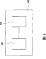
图4为本发明的一实施例的一种光电装置的示意图。FIG. 4 is a schematic diagram of an optoelectronic device according to an embodiment of the present invention.
附图标号:Figure number:
100、200:像素结构100, 200: pixel structure
100a、200a:基板100a, 200a: substrate
110a、210a:开关元件110a, 210a: switching elements
110b、210b:存储电容器110b, 210b: storage capacitors
112、212:第一金属层112, 212: first metal layer
112a、212a:栅极112a, 212a: grid
112b、212b:下电极112b, 212b: lower electrodes
112c、212c:焊垫112c, 212c: Welding pads
114、214:绝缘层114, 214: insulating layer
116、216’:主动层116, 216': active layer
118、218:第二金属层118, 218: second metal layer
118a、218a:源极118a, 218a: source
118b、218b:漏极118b, 218b: drain
118c、218c:上电极118c, 218c: upper electrode
118d、218d:导电图案118d, 218d: conductive pattern
120、220:保护层120, 220: protective layer
130、230:图案化有机材料层130, 230: patterning organic material layer
132a、132b、132c、232a、232b、232c:开口132a, 132b, 132c, 232a, 232b, 232c: openings
134、234:凸起图案134, 234: raised pattern
140、240:反射层140, 240: reflective layer
150、250:第一图案化光刻胶层150, 250: the first patterned photoresist layer
152a、152b、252a、252b:开口152a, 152b, 252a, 252b: openings
160、260:像素电极160, 260: pixel electrode
160a:保护电极160a: guard electrode
216:半导体层216: Semiconductor layer
216a:通道材料层216a: channel material layer
216b:欧姆接触层216b: Ohmic contact layer
219:第二图案化光刻胶层219: second patterned photoresist layer
219a:第一部分219a: Part I
219b、219b’:第二部分219b, 219b': Part II
300:显示面板300: display panel
310:像素阵列基板310: Pixel array substrate
320:另一基板320: another substrate
320a:透明电极320a: transparent electrode
330:显示介质330: display media
400:光电装置400: Photoelectric device
410:电子元件410: Electronic components
C1、C1’:第一接触窗C1, C1': first contact window
C2、C2’:第二接触窗C2, C2': second contact window
P1、P1’:像素区P1, P1': pixel area
P2、P2’:焊垫区P2, P2': pad area
具体实施方式 Detailed ways
为让本发明的上述和其他目的、特征和优点能更明显易懂,下文特举实施例,并配合所附图式作详细说明如下。In order to make the above and other objects, features and advantages of the present invention more comprehensible, the following specific embodiments are described in detail together with the accompanying drawings.
图1A至图1L为本发明的一实施例的一种像素结构的制造方法的剖面示意图。请先参考图1A,首先,提供一基板100a,其中基板100a具有一像素区P1与一焊垫区P2。接着,在基板100a上形成一第一金属层112。第一金属层112包括一栅极112a、一下电极112b以及一焊垫112c,其中栅极112a与下电极112b位于基板100a的像素区P1,焊垫112c位于基板100b的焊垫区P2。1A to 1L are schematic cross-sectional views of a method for manufacturing a pixel structure according to an embodiment of the present invention. Please refer to FIG. 1A. Firstly, a
值得一提的是,在本实施例的图式中,是以反射式像素结构为例来说明,但本发明较佳地应用于半穿透半反射式像素结构中或是微反射式像素结构中。另外,在本实施例的图式中,焊垫区P2是以扫描线焊垫区为例来说明。虽然图式未绘示出数据线焊垫区,但数据线焊垫区的结构与扫描线焊垫区相似,不同之处仅在于数据线焊垫区的焊垫是属于第二金属层,但图式出所绘示的扫描线焊垫区P2的焊垫112c是属于第一金属层112。再者,焊垫区P2的结构,不限于如下制作流程所述的结构。也就是说,不管焊垫区P2是以扫描线焊垫区或数据线焊垫区为例,其结构仅具有第一金属层、第二金属层、上述二金属层同时存在,并利用其它导电层来跨接上述二金属层、或上述二金属层的堆迭。于其它实施例中,像素结构可仅以像素区P1为主来说明与设计,而不用考虑焊垫区P2的设计与说明。It is worth mentioning that in the drawings of this embodiment, the reflective pixel structure is used as an example for illustration, but the present invention is preferably applied to a transflective pixel structure or a micro-reflective pixel structure middle. In addition, in the drawings of this embodiment, the pad region P2 is illustrated by taking the scanning line pad region as an example. Although the data line pad area is not shown in the figure, the structure of the data line pad area is similar to that of the scan line pad area, the only difference is that the pads in the data line pad area belong to the second metal layer, but The figure shows that the
另外,在本实施例中,基板110a的材质是包含无机透明材质(如:玻璃、石英、或其它合适材料、或上述的组合)、有机透明材质(如:聚烯类、聚酼类、聚醇类、聚酯类、橡胶、热塑性聚合物、热固性聚合物、聚芳香烃类、聚甲基丙酰酸甲酯类、聚碳酸酯类、或其它合适材料、或上述的衍生物、或上述的组合)、无机不透明材质(如:硅片、陶瓷、或其它合适材料、或上述的组合)、或上述的组合。In addition, in this embodiment, the material of the
此外,形成于基板100a上的第一金属层112,其材质较佳的是采用可进行湿法刻蚀的金属材料,但不限于此,于其他实施例中,亦可采用进行干法刻蚀的金属材料。第一金属层112可为单层结构或多层结构,在本实施例中,第一金属层112是以多层结构为范例,例如是钼或是钼-铝迭层或是钼-铝-钼迭层。然,本发明不限于此。在其他的实施例中,第一金属层112的材质可以是由金、银、铜、锡、铅、铪、钨、钼、钕、钛、钽、铝、锌等金属、上述合金、上述金属氧化物、上述金属氮化物、或上述的组合。In addition, the material of the
接着,请参考图1B,在第一金属层112上形成一绝缘层114,其覆盖像素区P1的栅极112a、下电极112b以及焊垫区P2的焊垫112c。在本实施例中,绝缘层114可为单层或多层结构,且其材质例如是无机材质(如:氧化硅、氮化硅、氮氧化硅、碳化硅、氧化铪、氧化铝、或其它材质、或上述的组合)、有机材质(如:光刻胶、苯并环丁烯(enzocyclobutane,BCB)、环烯类、聚酰亚胺类、聚酰胺类、聚酯类、聚醇类、聚环氧乙烷类、聚苯类、树脂类、聚醚类、聚酮类、或其它合适材料、或上述的组合)、或上述的组合。Next, please refer to FIG. 1B , an insulating
请参考图1C,在栅极112a上方的绝缘层114上形成一主动层116。详细而言,在本实施例中,主动层116的材质可以是非晶硅、单晶硅、微晶硅、多晶硅、或上述晶格的N型掺杂硅化物、或上述晶格的P型掺杂硅化物、或上述晶格的硅化锗、或其它材质、或上述的组合,而主动层116的结构可以是单层结构或者是多层结构。举例而言,主动层116可以是由非晶硅(a-Si)及/或N型重掺杂非晶硅所组成的单层结构,也可以是由非晶硅(a-Si)以及N型重掺杂非晶硅所组成的双层结构,其上述的结构排列,可为水平排列及/或垂直排列。在本实施例中主动层116是以非晶硅(亦称为通道层)以及N型重掺杂非晶硅(亦称为欧姆接触层)所组成的双层结构为实施范例,但不以此为限。Referring to FIG. 1C, an
接着,请参考图1D,在绝缘层114上形成一第二金属层118,其中第二金属层118包括位于像素区P1的部分主动层116上方的源极118a、漏极118b、于下电极112b上方的上电极118c以及位于焊垫区P2的导电图案118d。至此,在基板100a上已大致完成开关元件110a与存储电容器110b的制作。在此必需说明的是,上述开关元件110a与存储电容110b的制作方式与结构为本发明实施例的范例,并非限于此方式,亦可采用其它适用的结构或制作方式。此外,形成于绝缘层114上的第二金属层118,其材质较佳的是采用可进行湿法刻蚀的金属材料,但不限于此,亦可采用进行干法刻蚀的金属材料。第二金属层118可为单层结构或多层结构,在本实施例中,第二金属层118是以多层结构为范例,例如是钼或是钼-铝迭层或是钼-铝-钼迭层。然,本发明不限于此。在其他的实施例中,第二金属层118的材质可以是由金、银、铜、锡、铅、铪、钨、钼、钕、钛、钽、铝、锌等金属、上述合金、上述金属氧化物、上述金属氮化物、或上述的组合。Next, please refer to FIG. 1D, a
另外,必需说明的是,本发明的开关元件110a及其结构以底栅型结构为实施范例,但不限于此。于其它实施例中,仅只要变更第一金层层112及主动层116形成于基板100a上的顺序即可成为顶栅型结构。举例说明,于基板100a上形成主动层116,接着,于主动层116上形成一绝缘层114,其中绝缘层114覆盖像素区P1的主动层116。然后,在基板100a上形成第一金属层110a,其中第一金属层112包括栅极112a、下电极112b以及焊垫区P2的焊垫112c,而栅极112a在主动层116上方的绝缘层114上。之后,其余的步骤皆类似本发明上述实施例的方式。In addition, it must be noted that the switching
此外,为了得到较佳的电性特性,可在第一金属层112完成后,再覆盖内层介电层(未绘示)于该第一金属层112及绝缘层114上,则此顶栅型结构的第二金属层118就形成在内层介电层(未绘示),其中第二金属层118包括位于像素区P1的部分主动层116上方的源极118a、漏极118b、于下电极112b上方的上电极118c以及位于焊垫区P2的导电图案118d。至此,在基板100a上已大致完成开关元件110a与存储电容器110b的制作。In addition, in order to obtain better electrical characteristics, after the
请接着参考图1E,在基板100a上形成一保护层120,其中保护层120覆盖像素区P1的开关元件110a与存储电容器110b以及焊垫区P2的导电图案118d与绝缘层114。在本实施例中,保护层120可为单层或多层结构,且其材质为有机材质(例如:光刻胶、苯并环丁烯、环烯类、聚酰亚胺类、聚酰胺类、聚酯类、聚醇类、聚环氧乙烷类、聚苯类、树脂类、聚醚类、聚酮类、或其它材料、或上述的组合)、无机材质(例如是氧化硅、氮化硅、氮氧化硅、其他适合的材质或上述的组合)、或上述的组合。Referring to FIG. 1E , a
请参考图1F,接着,在保护层120上形成一图案化有机材料层130,其中部分图案化有机材料层130上形成有多个凸起图案134,且图案化有机材料层130具有多个开口132a、132b、132c。本发明实施例的凸起图案134是形成在像素区P1的有机材料层上,但不限于此,凸起图案134亦可形成于保护层120的表面、绝缘层114的表面、或其它合适的膜层上。开口132a暴露出位于像素区P1的漏极118b上的保护层120,开口132b暴露出位于像素区P1的上电极118c上方的保护层120,开口132c暴露出位于焊垫区P2的部分金属层118d与部分绝缘层114上方的保护层120。Please refer to FIG. 1F, then, a patterned
在本实施例中,图案化有机材料层130的形成方式是使用一灰阶掩膜(Grey-Level Mask,未绘示)、半透掩膜(Half-Tone Mask)、多阶掩膜(Multi-Tone Mask)或其它合适的掩膜,对一有机材料层(未绘示)来进行一曝光程序,其中灰阶掩膜是使用不同明暗度的掩膜,使有机材料层受到不同照度的曝光,经显影工艺之后可得到不同深浅度的形状,即形成图案化有机材料层130。此外,图案化有机材料层130的材质包括光刻胶、苯并环丁烯、环烯类、聚酰亚胺类、聚酰胺类、聚酯类、聚醇类、聚环氧乙烷类、聚苯类、树脂类、聚醚类、聚酮类、或其它材料、或上述的组合。In this embodiment, the patterned
请参考图1G,接着,在图案化有机材料层130上以及被暴露出的部分保护层120上形成一反射层140。也就是说,反射层140覆盖图案化有机材料层130的这些凸起图案134与部分保护层120,换言之,反射层140覆盖整个像素区P1与焊垫区P2或称为反射层140共形地形成于整个像素区P1与焊垫区P2上。此外,在本实施例中,反射层140可为单层结构或多层结构,且其材质可以是铝、铝合金、银或是其他具有高反射率的金属。另外,本发明实施例所述的凸起图案134于其它实施例中,亦可形成于反射层140的表面上。Referring to FIG. 1G , next, a
请参考图1H,接着,在像素区P1的反射层140上形成一第一图案化光刻胶层150,且第一图案化光刻胶层150具有多个开口152a、152b。更详细而言,第一图案化光刻胶层150暴露出位于焊垫区P2的反射层140,且第一图案化光刻胶层150的开口152a、152b暴露出位于像素区P1的部分反射层140,且开口152a实质上对应于开口132a,开口152b实质上对应于开口132b。Referring to FIG. 1H , next, a first
请同时参考图1I与图1J,接着,以第一图案化光刻胶层150作为刻蚀光掩膜,以移除位于像素区P1中被暴露出的部分反射层140以及位于被暴露出的部分反射层140底下的部分保护层120,而形成一第一接触窗C1以及一第二接触窗C2,其中第一接触窗C1暴露出开关元件110a的漏极118b,第二接触窗C2暴露出存储电容器110b的上电极118c。另外,在焊垫区P2中,反射层140完全被移除、部分保护层120被移除而暴露出部分的导电图案118d,以及部分保护层120与部分绝缘层114被移除而暴露出部分的焊垫112c。在此必需说明的是,当在移除位于被暴露出的部分反射层140底下的部分保护层120时(如像素区P1)是以第一图案化光刻胶层150与图案化有机材料层130作为刻蚀光掩膜。当移除被图案化有机材料层130所暴露出的部分保护层120(如焊垫区P2)时是以图案化有机材料层130作为刻蚀光掩膜。在本实施例中,移除被暴露出的部分反射层140以及位于被暴露出的部分反射层140底下的部分保护层120的较佳方法包括湿法刻蚀,但不限于此,亦可采用合适的干法刻蚀。Please refer to FIG. 1I and FIG. 1J at the same time. Next, the first
详细而言,在本实施例中,移除被暴露出的反射层140以及位于被暴露出的部分反射层140底下的保护层120是采用原位程序(in-situ process)。也就是说,移除被暴露出的反射层140以及位于被暴露出的部分反射层140底下的保护层120时,可以在相同的反应室中以不同的刻蚀液依序刻蚀反射层140以及保护层120来完成。也就是说,仅有一次光刻工艺或称为仅有一个或同一个图案化光刻胶层,但同时完成反射层140刻蚀与保护层120刻蚀。In detail, in this embodiment, an in-situ process is used to remove the exposed
请参考图1K,接着,移除第一图案化光刻胶层150,以暴露出反射层140。接着,请参考图1L,在像素区P1的反射层140与部分图案化有机材料层130上形成一像素电极160且在焊垫区P2的有机材料层130上形成保护电极160a。特别是,像素电极160通过第一接触窗C1与开关元件110a的漏极118b电连接,且像素电极160通过第二接触窗C2与存储电容器110b的上电极118c电连接。导电图案118d与焊垫112c通过保护电极160a而彼此电连接。至此,像素结构100已大致完成。Referring to FIG. 1K , next, the first
详细而言,实务上,形成像素电极160以及保护电极160a的方法例如是以物理汽相沉积(Physical Vapor Deposition,PVD)法的溅射工艺所形成,但不限于此,亦可使用网版印刷法、喷墨法或其它合适的方法。像素电极160以及保护电极160a可以为单层或多层结构,且其材质可视像素结构100的显示模式设计而有所不同。举例而言,像素电极160以及保护电极160a可以是由透明导电材质制成例如是铟锡氧化物、铟锌氧化物、铟锡锌氧化物、氧化铪、氧化锌、氧化铝、铝锡氧化物、铝锌氧化物、镉锡氧化物、镉锌氧化物或上述的组合。较佳地,像素电极160与保护电极160a是同时形成的,但不限于此,二者亦可不同时形成。In detail, in practice, the method of forming the
在本发明中,由于移除被暴露出的部分反射层140以及位于被暴露出的部分反射层140底下的部分保护层120是利用同一图案化光刻胶层作为刻蚀光掩膜,并可采用原位程序的方式依序,因此相较于已知反射式液晶显示器的像素结构的制造方法而言,本实施例可省略至少一次光刻工艺,以减少掩膜使用数,并可缩短像素结构100的工艺时间以降低生产成本。另外,本实施例是采用可进行湿法刻蚀的钼或钼及铝的迭层作为第一金属层112与第二金属层118为较佳范例,但不限于此。由于湿法刻蚀工艺相较于干法刻蚀工艺快,因此可以增加产能。此外,当进行湿法刻蚀时,由于有保护层120保护第二金属层118,因此可以避免第二金属层118受到刻蚀液的侵蚀。In the present invention, the same patterned photoresist layer is used as an etching photomask to remove the exposed partial
特别值得一提的是,上述实施例是以反射式像素结构为例来说明,因而反射层140会覆盖整个像素区P1。然而,本发明较佳地应用于半穿透半反射式像素结构中或是微反射式像素结构中。若上述实施例是应用于半穿透半反射式像素结构或微反射式像素结构,则基板100a的像素区P1中可分为至少一反射区与至少一穿透区(未绘示)或至少一微反射区与至少一穿透区(未绘示)。而当后续形成图案化有机材料层130以及反射层140时,其中图案化有机材料层130上的凸起图案134以及反射层140仅会形成在反射区中。It is particularly worth mentioning that the above-mentioned embodiment is described with a reflective pixel structure as an example, so the
图2A至图2N为本发明的另一实施例的一种像素结构的制造方法的剖面示意图。请先参考图2A,首先,提供一基板200a,其中基板200a具有一像素区P1’与一焊垫区P2’。接着于基板200a上形成一第一金属层112,第一金属层212包括一栅极212a、一下电极212b以及一焊垫212c,其中栅极212a与下电极212b位于基板200a的像素区P1’,焊垫212c位于基板200b的焊垫区P2’。此外,基板200a的材质、第一金属层212的材质、焊垫212c的设计以及焊垫212c的结构如先前段落描述(对应图1A的基板100a与第一金属层112的段落),故在此不再赘述。于其它实施例中,像素结构,可仅以像素区P1’为主来说明与设计,而不用考虑焊垫区P2’的说明与设计。2A to 2N are schematic cross-sectional views of a method for manufacturing a pixel structure according to another embodiment of the present invention. Please refer to FIG. 2A. Firstly, a
请参考图2B,接着,在第一金属层212上依序形成一绝缘层214、一半导体层216以及一第二金属层218。也就是说,绝缘层214覆盖像素区P1’的栅极212a、下电极212b以及焊垫区P2’的焊垫212c,半导体层216覆盖绝缘层214,第二金属层218覆盖半导体层216,换言之,绝缘层214、半导体层216以及第二金属层218依序堆迭在一起。值得一提的是,在本实施例中,半导体层216可由一通道层216a以及一欧姆接触层216b以垂直排列所组成为范例,但不限于此,亦可水平排列。其中,通道层216a的材料包括非晶硅、单晶硅、微晶硅、多晶硅、或其它合适的材料、或上述的组合。在本实施例中通道层是以非晶硅(a-Si)为实施范例,但不以此为限。另外,欧姆接触层216b的材料包括N型掺杂非晶硅、P型掺杂非晶硅、N型掺杂/P型掺杂单晶硅、N型掺杂/P型掺杂微晶硅、N型掺杂/P型掺杂多晶硅、或其它合适的材料、或上述的组合。在本实施例中欧姆接触层216b是以N型重掺杂非晶硅为实施范例,但不以此为限。此外,绝缘层214以及第二金属层218的材质如先前段落描述(对应图1B的绝缘层214与图1D第二金属层118的段落),故在此不再赘述。Referring to FIG. 2B , next, an insulating
请参考图2C,接着,在第二金属层218上形成一第二图案化光刻胶层219。第二图案化光刻胶层219具有一第一部分219a与一第二部分219b,其中第一部分219a覆盖住栅极212a上方,第二部分219b覆盖住栅极212a两侧上方的第二金属层218、下电极212b上方的第二金属层218以及焊垫区P2的导电图案218d。Referring to FIG. 2C , next, a second
详细而言,第二图案化光刻胶层219是以一灰阶掩膜(未绘示)、半透掩膜(Half-Tone Mask)、多阶掩膜(Multi-Tone Mask)或其它合适的掩膜,对一光刻胶层(未绘示)进行一曝光程序所形成,其中灰阶掩膜是使用不同明暗度的掩膜,使光刻胶层受到不同照度的曝光,经显影工艺之后可得到不同深浅度的形状,即形成第二图案化光刻胶层219的第一部分219a与第二部分219b,并暴露出部分的第二金属层218,其中,第一部分219a的厚度实质上小于第二部分219b的厚度。In detail, the second
请参考图2D,接着,以第二图案化光刻胶层219为光掩膜,来刻蚀被暴露出的部分的第二金属层218与其底下的膜层(如:216),以图案化第二金属层218与半导体层216,并于栅极212a上方定义出一主动层216’、于下电极212b上方定义出上电极218c且于焊垫区P2’定义出导电图案218d。此时,未被第二图案化光刻胶层219所遮蔽的区域就会暴露出部分的绝缘层214。详细而言,本实施例的主动层216’的材质同上述图2B的半导体层216的通道层216a的材质,其皆是以非晶硅(a-Si)为实施范例,但不以此为限。Please refer to FIG. 2D, and then, use the second
请参考图2E,接着,对第二图案化光刻胶层219进行一灰化程序,以控制灰化工艺中第二图案化光刻胶层219被刻蚀的厚度,以完全移除第一部分219a,而形成薄化后的第二部分219b’会暴露出主动层216’上方的部分第二金属层218。Please refer to FIG. 2E, then, an ashing process is performed on the second
接着,请参考图2F及2G,以第二图案化光刻胶层219薄化后的第二部分219b’作为光掩膜,以移除主动层216’上方的第二金属层218,以定义出源极218a以及漏极218b,并移除部分的部分欧姆接触层216b,而暴露出部分主动层216’。之后,在移除薄化后的第二部分219b’,以暴露出位于像素区P1的源极218a、漏极218b以及上电极218c与焊垫区P2的导电图案218d,如图2G所示。特别是,在本实施例中,主动层216’作为源极218a及漏极218b之间的电子通道,而欧姆接触层216b则可降低第二金属层218的源极218a/漏极218b与主动层216’之间的接触阻抗。至此,在基板200a上已大致完成开关元件210a与存储电容器210b。其中,本实施例是以底栅型结构为范例,但不限于此,亦可使用上述实施例所述的顶栅型结构。在此必需说明的是,上述开关元件110a与存储电容110b的制作方式与结构为本发明实施例的范例,并非限于此方式,亦可采用其它适用的结构或制作方式。Next, please refer to FIG. 2F and 2G, use the thinned
请继续参考图2G,接着,在基板200a上形成一保护层220,其中保护层220覆盖像素区P1’的开关元件210a与存储电容器210b以及焊垫区P2’的导电图案218d。此外,保护层220的材质如先前段落描述(对应图1E的保护层120的段落),故在此不再赘述。Please continue to refer to FIG. 2G. Next, a
请参考图2H,接着,在保护层220上形成一图案化有机材料层230,其中部分图案化有机材料层230上形成有多个凸起图案234,且图案化有机材料层230具有多个开口232a、232b、232c。本发明实施例的凸起图案234是形成在像素区P1的有机材料层上,但不限于此,凸起图案234亦可形成于保护层220的表面、绝缘层214的表面、或其它合适的膜层上。开口232a暴露出位于像素区P1’的漏极218b上的保护层220,开口232b暴露出位于像素区P1’的上电极218c上方的保护层220,开口232c暴露出位于焊垫区P2’的部分金属层218d与部分绝缘层214上方的保护层220。Please refer to FIG. 2H, then, a patterned
在本实施例中,图案化有机材料层230的形成方式是使用一灰阶掩膜(Grey-Level Mask)(未绘示)、半透掩膜(Half-Tone Mask)、多阶掩膜(Multi-Tone Mask)或其它合适的掩膜,对一有机材料层(未绘示)来进行一曝光程序,其中灰阶掩膜是使用不同明暗度的掩膜,使有机材料层受到不同照度的曝光,经显影工艺之后可得到不同深浅度的形状,即形成图案化有机材料层230。此外,图案化有机材料层230的材质如先前段落描述(对应图1F的图案化有机材料层130的段落),故在此不再赘述。In this embodiment, the patterned
请参考图2I,接着,在图案化有机材料层230上以及被暴露出的部分保护层220上形成一反射层240。也就是说,反射层240覆盖图案化有机材料层230的这些凸起图案234与部分保护层220,换言之,反射层240覆盖整个像素区P1’与焊垫区P2’或称为反射层240共形地形成于整个像素区P1’与焊垫区P2’上。在本实施例中,反射层240可为单层结构或多层结构,且其材质可以是铝、铝合金、银或是其他具有高反射率的金属。另外,本发明实施例所述的凸起图案134的位置仅为举例说明,于其它未绘示的实施例中,亦可形成于反射层140的表面上。Referring to FIG. 2I , next, a
请参考图2J,接着,在像素区P1’的部分反射层240上形成一第一图案化光刻胶层250,且第一图案化光刻胶层250具有多个开口252a、252b。更详细而言,第一图案化光刻胶层150暴露出位于焊垫区P2’的反射层240,且第一图案化光刻胶层250的这些开口252a、252b以暴露出部分反射层240,且开口252a实质上对应于开口232a,开口252b实质上对应于开口232b。Referring to FIG. 2J , next, a first
请同时参考图2K与图2L,接着,以第一图案化光刻胶层250作为刻蚀光掩膜,以移除位于像素区P1’中被暴露出的部分反射层240以及位于被暴露出的部分反射层240底下的部分保护层220,而形成一第一接触窗C1’以及一第二接触窗C2’,其中第一接触窗C1’暴露出开关元件210a的漏极218b,第二接触窗C2’暴露出存储电容器210b的上电极218c。另外,在焊垫区P2’中,反射层240完全被移除、部分保护层220被移除而暴露出部分的导电图案218d,以及部分保护层220与部分绝缘层214被移除而暴露出部分的焊垫212c。在此必需说明的是,当在移除位于被暴露出的部分反射层140底下的部分保护层220时(如像素区P1)是以第一图案化光刻胶层250与图案化有机材料层230作为刻蚀光掩膜。当移除被图案化有机材料层230所暴露出的部分保护层220(如焊垫区P2)时是以图案化有机材料层230作为刻蚀光掩膜。在本实施例中,移除被暴露出的部分反射层240以及位于被暴露出的部分反射层240底下的部分保护层220的较佳方法包括湿法刻蚀,但不限于此,亦可采用合适的干法刻蚀。Please refer to FIG. 2K and FIG. 2L at the same time. Next, use the first
详细而言,在本实施例中,移除被暴露出的反射层240以及位于被暴露出的部分反射层240底下的保护层220是采用原位程序(in-situ process)。也就是说,移除被暴露出的反射层240以及位于被暴露出的部分反射层240底下的保护层220时,可以在相同的反应室中以不同的刻蚀液依序刻蚀反射层240以及保护层220来完成。也就是说,仅有一次光刻工艺或称为仅有一个或同一个图案化光刻胶层,但同时完成反射层240刻蚀与保护层220刻蚀。In detail, in this embodiment, an in-situ process is used to remove the exposed
请参考图2M,接着,移除第一图案化光刻胶层250,以暴露出反射层240。接着,请参考图2N,在像素区P1’的反射层240与部分图案化有机材料层230上形成一像素电极260且在焊垫区P2’的有机材料层230上形成保护电极260a。特别是,像素电极260通过第一接触窗C1’与开关元件210a的漏极218b电连接,且像素电极260通过第二接触窗C2’与存储电容器210b的上电极218c电连接。导电图案218d与焊垫212c通过保护电极260a而彼此电连接。在本实施例中,像素电极260的材质如先前段落描述(对应图1L的像素电极160的段落),故在此不再赘述。至此,像素结构200已大致完成。较佳地,像素电极260与保护电极260a是同时形成的,但不限于此,二者亦可不同时形成。Referring to FIG. 2M , next, the first
类似地,本实施例同样可省略至少一次光刻工艺,以减少掩膜使用数,并可缩短像素结构200的工艺时间以降低生产成本。另外,本实施例若采用湿法刻蚀工艺来刻蚀第一金属层212与第二金属层218还可增加产能。此外,当进行湿法刻蚀时,由于有保护层220保护第二金属层218,因此同样可以避免第二金属层218受到刻蚀液的侵蚀。Similarly, in this embodiment, at least one photolithography process can be omitted to reduce the number of masks used, and the process time of the
需再次说明的是,上述实施例是以反射式像素结构为例来说明,因而反射层240会覆盖整个像素区P1’。然而,本发明较佳地应用于半穿透半反射式像素结构中或是微反射式像素结构中。若上述实施例是应用于半穿透半反射式像素结构,则基板200a的像素区P1’中可分为至少一反射区与至少一穿透区(未绘示)或至少一微反射区与至少一穿透区(未绘示)。而当后续形成图案化有机材料层230以及反射层240时,其中图案化有机材料层230上的凸起图案234以及反射层240仅会形成在反射区中。It should be noted again that the above embodiment is described by taking the reflective pixel structure as an example, so the
图3为本发明的一实施例的一种显示面板的示意图。请参照图3,本实施例的显示面板300的成品包括至少一像素阵列基板310、一相对于此像素阵列基板310的另一基板320及一设置于像素阵列基板310与另一基板320之间的显示介质320,其中像素阵列基板310具有上述如图1L所示的像素结构100或如图2N所示的像素结构200,且另一基板320选择性地具有一透明电极320a。显示面板300的制造方法包含如上所述的像素结构100或像素结构200的制造方法,再依照各种显示面板300的制造程序并组装,以获得显示装置300。FIG. 3 is a schematic diagram of a display panel according to an embodiment of the present invention. Please refer to FIG. 3 , the finished product of the
此外,当显示介质330为光电偏折材料时,例如为液晶材料,则显示面板300可为半穿透半反射式显示面板、微反射式显示面板反射型显示面板、彩色滤光片于主动层上(color filter on array)的显示面板、主动层于彩色滤光片上(array on color filter)的显示面板、垂直配向型(VA)显示面板、水平切换型(IPS)显示面板、多域垂直配向型(MVA)显示面板、扭曲向列型(TN)显示面板、超扭曲向列型(STN)显示面板、图案垂直配向型(PVA)显示面板、超级图案垂直配向型(S-PVA)显示面板、先进大视角型(ASV)显示面板、边缘电场切换型(FFS)显示面板、连续焰火状排列型(CPA)显示面板、轴对称排列微单元型(ASM)显示面板、光学补偿弯曲排列型(OCB)显示面板、超级水平切换型(S-IPS)显示面板、先进超级水平切换型(AS-IPS)显示面板、极端边缘电场切换型(UFFS)显示面板、高分子稳定配向型显示面板、双视角型(dual-view)显示面板、三视角型(triple-view)显示面板、三维显示面板(three-dimensional)、多面显示面板(multi-panel)、或其它型面板。若显示介质330为电激发光材料,显示面板300则称为电激发光显示面板(如:磷光电激发光显示面板、荧光电激发光显示面板、或上述的组合),亦称为自发光显示面板,且其电激发光材料可为有机材料、有机材料、无机材料、或上述的组合,再者,上述材料的分子大小包含小分子、高分子、或上述的组合。若,显示介质330同时包含液晶材料及电激发光材料,则显示面板300称为混合式(hybrid)显示面板或半自发光显示面板。In addition, when the
图4为本发明的一实施例的一种光电装置的示意图。请参考图4,由上述实施例所述的的显示面板300可以跟电子元件410电连接而组合成一光电装置400,而光电装置400的制造方法,包含如上所述的显示面板300的制造方法,再依照各种光电装置400的制造程序并组装所得显示器,以获得光电装置400。由于,在本实施例中,显示面板300是采用上述的像素结构100(请参考图1L)或像素结构200(请参考图2N)作为像素阵列基板310(请参考图3),因此采用上述的像素结构100或像素结构200的光电装置400除了可降低工艺时间增加产率外,同时还可降低生产成本。FIG. 4 is a schematic diagram of an optoelectronic device according to an embodiment of the present invention. Please refer to FIG. 4 , the
另外,电子元件410包括如:控制元件、操作元件、处理元件、输入元件、记忆元件、驱动元件、发光元件、保护元件、感测元件、检测元件、或其它功能元件、或前述的组合。而光电装置400的类型包括可携式产品(如手机、摄影机、照相机、笔记本电脑、游戏机、手表、音乐播放器、电子信件收发器、地图导航器、数字相片、或类似的产品)、影音产品(如影音播放器或类似的产品)、荧幕、电视、看板、投影机内的面板等。In addition, the
虽然本发明已以实施例揭露如上,然其并非用以限定本发明,任何所属技术领域中具有通常知识的技术人员,在不脱离本发明的精神和范围内,当可作些许的更动与润饰,故本发明的保护范围当视所附的权利要求范围所界定为准。Although the present invention has been disclosed above with embodiments, it is not intended to limit the present invention. Any skilled person in the technical field with common knowledge can make some modifications and changes without departing from the spirit and scope of the present invention. Modification, so the scope of protection of the present invention should be defined by the scope of the appended claims.
Claims (8)
Priority Applications (1)
| Application Number | Priority Date | Filing Date | Title |
|---|---|---|---|
| CNA2008101696999A CN101382715A (en) | 2008-10-20 | 2008-10-20 | Pixel structure, display panel and manufacturing method of photoelectric device |
Applications Claiming Priority (1)
| Application Number | Priority Date | Filing Date | Title |
|---|---|---|---|
| CNA2008101696999A CN101382715A (en) | 2008-10-20 | 2008-10-20 | Pixel structure, display panel and manufacturing method of photoelectric device |
Publications (1)
| Publication Number | Publication Date |
|---|---|
| CN101382715A true CN101382715A (en) | 2009-03-11 |
Family
ID=40462624
Family Applications (1)
| Application Number | Title | Priority Date | Filing Date |
|---|---|---|---|
| CNA2008101696999A Pending CN101382715A (en) | 2008-10-20 | 2008-10-20 | Pixel structure, display panel and manufacturing method of photoelectric device |
Country Status (1)
| Country | Link |
|---|---|
| CN (1) | CN101382715A (en) |
Cited By (5)
| Publication number | Priority date | Publication date | Assignee | Title |
|---|---|---|---|---|
| CN102419931A (en) * | 2011-11-18 | 2012-04-18 | 友达光电股份有限公司 | Display panel |
| CN103676467A (en) * | 2012-09-20 | 2014-03-26 | 李永春 | Metal-embedded mask and method for manufacturing the same |
| CN104952882A (en) * | 2015-03-26 | 2015-09-30 | 友达光电股份有限公司 | Active element array substrate |
| CN111627933A (en) * | 2019-12-10 | 2020-09-04 | 友达光电股份有限公司 | Active element substrate and method of manufacturing the same |
| WO2022134029A1 (en) * | 2020-12-25 | 2022-06-30 | 京东方科技集团股份有限公司 | Display panel, method for manufacturing display panel, and display device |
-
2008
- 2008-10-20 CN CNA2008101696999A patent/CN101382715A/en active Pending
Cited By (9)
| Publication number | Priority date | Publication date | Assignee | Title |
|---|---|---|---|---|
| CN102419931A (en) * | 2011-11-18 | 2012-04-18 | 友达光电股份有限公司 | Display panel |
| CN102419931B (en) * | 2011-11-18 | 2013-09-04 | 友达光电股份有限公司 | Display panel |
| CN103676467A (en) * | 2012-09-20 | 2014-03-26 | 李永春 | Metal-embedded mask and method for manufacturing the same |
| CN103676467B (en) * | 2012-09-20 | 2019-05-21 | 李永春 | Metal-embedded mask and method for manufacturing the same |
| CN104952882A (en) * | 2015-03-26 | 2015-09-30 | 友达光电股份有限公司 | Active element array substrate |
| CN104952882B (en) * | 2015-03-26 | 2018-02-09 | 友达光电股份有限公司 | Active element array substrate |
| CN111627933A (en) * | 2019-12-10 | 2020-09-04 | 友达光电股份有限公司 | Active element substrate and method of manufacturing the same |
| CN111627933B (en) * | 2019-12-10 | 2023-04-18 | 友达光电股份有限公司 | Active element substrate and manufacturing method thereof |
| WO2022134029A1 (en) * | 2020-12-25 | 2022-06-30 | 京东方科技集团股份有限公司 | Display panel, method for manufacturing display panel, and display device |
Similar Documents
| Publication | Publication Date | Title |
|---|---|---|
| US20250151410A1 (en) | Electronic device | |
| US9443886B2 (en) | Thin film transistor substrate and method of fabricating the same | |
| JP4277874B2 (en) | Manufacturing method of electro-optical device | |
| US7842953B2 (en) | Pixel structure and repairing method thereof | |
| US8253905B2 (en) | Liquid crystal display device and method of making the same | |
| CN101419987B (en) | Semiconductor device and method for manufacturing the same | |
| US8772796B2 (en) | Panel and method for fabricating the same | |
| US20100055850A1 (en) | Methods for fabricating pixel structure, display panel and electro-optical apparatus | |
| CN101409263B (en) | Pixel structure, display panel and manufacturing method of photoelectric device | |
| CN101236976B (en) | Active element array substrate, optoelectronic device and manufacturing method thereof | |
| US20080042132A1 (en) | Display panel and method for manufacturing the same | |
| CN101382715A (en) | Pixel structure, display panel and manufacturing method of photoelectric device | |
| CN100533747C (en) | pixel structure and repairing method thereof | |
| CN100550396C (en) | Pixel and forming method thereof, storage capacitor, display panel and photoelectric device | |
| US8134662B2 (en) | Pixel structure of transflective liquid crystal display array substrate and method for fabricating the same | |
| US20100072476A1 (en) | Pixel structure, display panel, photoelectric device and manufacturing method thereof | |
| US20080055504A1 (en) | Making dual side displays | |
| US7738049B2 (en) | Active device array substrate, electro-optical apparatus and method for fabricating the same | |
| US8212987B2 (en) | Liquid crystal display device and the manufacturing method thereof | |
| CN113433741B (en) | Array substrate, manufacturing method of array substrate and display device | |
| CN110244496B (en) | Display panel and method of making the same | |
| CN101299441B (en) | Thin film transistor, thin film transistor array substrate, display panel and photoelectric device | |
| JP2006319032A (en) | Multilayer diode, diode device and manufacturing method thereof | |
| CN101162337A (en) | Pixel structure and manufacturing method of transflective liquid crystal display array substrate | |
| CN101075623B (en) | Pixel structure and its formation method |
Legal Events
| Date | Code | Title | Description |
|---|---|---|---|
| C06 | Publication | ||
| PB01 | Publication | ||
| C10 | Entry into substantive examination | ||
| SE01 | Entry into force of request for substantive examination | ||
| C02 | Deemed withdrawal of patent application after publication (patent law 2001) | ||
| WD01 | Invention patent application deemed withdrawn after publication |
Open date: 20090311 |