CN101305571B - Image suppression receiver - Google Patents
Image suppression receiver Download PDFInfo
- Publication number
- CN101305571B CN101305571B CN2006800414462A CN200680041446A CN101305571B CN 101305571 B CN101305571 B CN 101305571B CN 2006800414462 A CN2006800414462 A CN 2006800414462A CN 200680041446 A CN200680041446 A CN 200680041446A CN 101305571 B CN101305571 B CN 101305571B
- Authority
- CN
- China
- Prior art keywords
- signal
- mentioned
- image
- circuit
- output
- Prior art date
- Legal status (The legal status is an assumption and is not a legal conclusion. Google has not performed a legal analysis and makes no representation as to the accuracy of the status listed.)
- Expired - Fee Related
Links
Images




Classifications
-
- H—ELECTRICITY
- H03—ELECTRONIC CIRCUITRY
- H03D—DEMODULATION OR TRANSFERENCE OF MODULATION FROM ONE CARRIER TO ANOTHER
- H03D7/00—Transference of modulation from one carrier to another, e.g. frequency-changing
- H03D7/18—Modifications of frequency-changers for eliminating image frequencies
-
- H—ELECTRICITY
- H04—ELECTRIC COMMUNICATION TECHNIQUE
- H04B—TRANSMISSION
- H04B1/00—Details of transmission systems, not covered by a single one of groups H04B3/00 - H04B13/00; Details of transmission systems not characterised by the medium used for transmission
- H04B1/06—Receivers
- H04B1/16—Circuits
- H04B1/26—Circuits for superheterodyne receivers
- H04B1/28—Circuits for superheterodyne receivers the receiver comprising at least one semiconductor device having three or more electrodes
-
- H—ELECTRICITY
- H04—ELECTRIC COMMUNICATION TECHNIQUE
- H04L—TRANSMISSION OF DIGITAL INFORMATION, e.g. TELEGRAPHIC COMMUNICATION
- H04L27/00—Modulated-carrier systems
- H04L27/32—Carrier systems characterised by combinations of two or more of the types covered by groups H04L27/02, H04L27/10, H04L27/18 or H04L27/26
- H04L27/34—Amplitude- and phase-modulated carrier systems, e.g. quadrature-amplitude modulated carrier systems
- H04L27/36—Modulator circuits; Transmitter circuits
- H04L27/366—Arrangements for compensating undesirable properties of the transmission path between the modulator and the demodulator
-
- H—ELECTRICITY
- H04—ELECTRIC COMMUNICATION TECHNIQUE
- H04L—TRANSMISSION OF DIGITAL INFORMATION, e.g. TELEGRAPHIC COMMUNICATION
- H04L27/00—Modulated-carrier systems
- H04L27/32—Carrier systems characterised by combinations of two or more of the types covered by groups H04L27/02, H04L27/10, H04L27/18 or H04L27/26
- H04L27/34—Amplitude- and phase-modulated carrier systems, e.g. quadrature-amplitude modulated carrier systems
- H04L27/38—Demodulator circuits; Receiver circuits
- H04L27/3818—Demodulator circuits; Receiver circuits using coherent demodulation, i.e. using one or more nominally phase synchronous carriers
Landscapes
- Engineering & Computer Science (AREA)
- Computer Networks & Wireless Communication (AREA)
- Signal Processing (AREA)
- Power Engineering (AREA)
- Superheterodyne Receivers (AREA)
- Digital Transmission Methods That Use Modulated Carrier Waves (AREA)
- Noise Elimination (AREA)
Abstract
Description
技术领域technical field
本发明涉及作为无线通信的接收电路的镜像抑制(imagesuppression)接收机,特别是涉及在外差接收机等中使用的镜像抑制接收机的高性能化,涉及修正I信号与Q信号的信号间误差的方法。The present invention relates to an image suppression (image suppression) receiver as a receiving circuit for wireless communication, and in particular to improvement of the performance of an image suppression receiver used in a heterodyne receiver and the like, and to correction of an error between signals of an I signal and a Q signal method.
背景技术Background technique
图7表示在一般的外差接收机中使用的镜像抑制接收机100。(例如,参照非专利文献1,p153,图5.25。图7的电路在本文献的电路中添加了LNA2、ADC9、数字信号处理电路10。)Figure 7 shows an
图7中,2是低噪声放大器(LNA),3-1、3-2分别是I用乘法器、Q用乘法器,4是PLL、5-1、5-2是LPF,6是镜像抑制电路,7是相位器,8是加法器,9是AD转换器,10是数字信号处理电路。In Fig. 7, 2 is a low noise amplifier (LNA), 3-1 and 3-2 are multipliers for I and multipliers for Q respectively, 4 is PLL, 5-1 and 5-2 are LPF, and 6 is image rejection Circuit, 7 is a phaser, 8 is an adder, 9 is an AD converter, and 10 is a digital signal processing circuit.
其次,说明动作的概况。Next, an outline of the operation will be described.
所接收的RF信号由作为低噪声放大器的LNA2放大。用LNA2放大了的RF信号分支为2个,分别与PLL4生成的LOI信号、LOQ信号在乘法器3-1、3-2中相乘,生成作为IF信号的I信号、Q信号。对I信号和Q信号由LPF5-1、5-2去除不需要的信号。由LPF5-1、5-2去除了不需要的信号的I信号、Q信号输入到镜像抑制电路6。镜像抑制电路6由移相电路7和加法器8构成。由LPF5-1进行了滤波的I信号在移相电路7中移相π/2,与通过了LPF5-2的Q信号在加法器8中相加。对加法器8的输出由ADC9从模拟信号变换成数字信号。变换为数字信号的信号在数字信号处理电路10中进行数字信号处理。The received RF signal is amplified by LNA2 as a low noise amplifier. The RF signal amplified by the LNA2 is divided into two branches, and multiplied by the LOI signal and the LOQ signal generated by the PLL4 respectively in the multipliers 3-1 and 3-2 to generate an I signal and a Q signal as IF signals. For the I signal and the Q signal, unnecessary signals are removed by LPF 5-1 and 5-2. The I signal and the Q signal from which unnecessary signals have been removed by the LPFs 5 - 1 and 5 - 2 are input to the
这里,RF信号的频率例如是1GHz,LOI信号和LOQ信号是999MHz,IF信号是1MHz。LOI信号和LOQ信号的频率相同,而相位错开π/2。另外,滤波器的截止频率取为1.5MHz,1MHz信号无损失地通过。Here, the frequency of the RF signal is, for example, 1 GHz, the frequency of the LOI signal and the LOQ signal is 999 MHz, and the frequency of the IF signal is 1 MHz. The frequency of the LOI signal and the LOQ signal are the same, but the phases are staggered by π/2. In addition, the cutoff frequency of the filter is taken as 1.5MHz, and the 1MHz signal passes through without loss.
其次,说明动作的详细过程。Next, the detailed procedure of the operation will be described.
在RF信号中,通常希望波和镜像波混合存在。希望波是希望接收的频率的信号。镜像波是隔着LO信号与希望波相反的频率的信号。这种情况下,镜像波的频率成为998MHz。In RF signals, there is usually a mixture of desired and image waves. The desired wave is a signal of a frequency desired to be received. The image wave is a signal having an opposite frequency to the desired wave across the LO signal. In this case, the frequency of the image wave becomes 998 MHz.
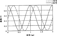
镜像信号频率和希望波信号频率分别在乘法器3-1、3-2中与LO信号相乘,在由LPF5-1、5-2滤波以后,成为相同的频率。然而,镜像频率的I信号和Q信号的相位关系与希望波的相位关系不同。如图8所示,镜像频率的情况下,I信号和Q信号的信号振幅一致,但是I信号的相位滞后π/2。希望波的情况与此相反,Q信号的相位滞后π/2。镜像信号的情况下,由镜像抑制电路6的相位器7进一步滞后π/2,作为结果I信号滞后π。如果振幅相同相位错开π,则合成的信号的振幅成为0。与此不同,希望波信号如果通过镜像抑制电路6则信号振幅成为2倍。这样,镜像信号由镜像抑制电路6去除,在镜像抑制电路6的输出中仅出现希望波。The image signal frequency and the desired wave signal frequency are multiplied by the LO signal in the multipliers 3-1 and 3-2, respectively, and filtered by the LPFs 5-1 and 5-2 to become the same frequency. However, the phase relationship between the I signal and the Q signal at the image frequency is different from that of the desired wave. As shown in FIG. 8 , in the case of the image frequency, the signal amplitudes of the I signal and the Q signal are the same, but the phase of the I signal lags by π/2. In the case of the desired wave, on the contrary, the phase of the Q signal lags by π/2. In the case of an image signal, it is further delayed by π/2 by the phaser 7 of the
图9表示该镜像抑制电路6的传递特性。如图9所示,希望波的信号无损失地通过,而镜像频率衰减。这样构成镜像抑制接收机100。FIG. 9 shows transfer characteristics of the
在外差接收机中,这样的镜像抑制电路特别是在IF频率相对于RF频率为1/100以下的Low-IF方式的情况下是必须的。In a heterodyne receiver, such an image suppression circuit is necessary especially in the case of the Low-IF system in which the IF frequency is 1/100 or less relative to the RF frequency.
非专利文献1:黑田忠弘监译,Behzad Razavi著,“RF微电子学”,丸善株式会社出版Non-Patent Document 1: Translated under the supervision of Tadahiro Kuroda, written by Behzad Razavi, "RF Microelectronics", published by Maruzen Co., Ltd.
然而,在上述现有的镜像抑制接收机100中,在由于元件偏差等而发生了I信号或者Q信号的信号之间的相位误差或者振幅误差的情况下,存在镜像抑制特性恶化这样的问题。镜像抑制比(IRR)近似为(式1)。(参照非专利文献1的p156)However, in the conventional
IRR={(ΔA/A)2+(ΔP)2}/4 (式1)IRR={(ΔA/A) 2 +(ΔP) 2 }/4 (Formula 1)
这里,ΔA是振幅误差,A是信号振幅,ΔP是相位误差。Here, ΔA is the amplitude error, A is the signal amplitude, and ΔP is the phase error.
图10表示计算了基于相位误差和振幅误差的IRR的影响的结果。相位误差是3°,振幅误差是0.5dB时,镜像抑制成为小于等于30dB。在通常的接收机中,要求镜像抑制大于等于30dB。特别是,在制造偏差大的CMOS半导体工艺中,有时I信号与Q信号的信号间误差变得更大,成为很大的问题。FIG. 10 shows the results of calculating the influence of the IRR based on the phase error and the amplitude error. When the phase error is 3° and the amplitude error is 0.5dB, the image rejection becomes 30dB or less. In a common receiver, image rejection is required to be greater than or equal to 30dB. In particular, in a CMOS semiconductor process in which manufacturing variations are large, the inter-signal error between the I signal and the Q signal may become larger and become a serious problem.
发明内容Contents of the invention
本发明是为解决上述课题而完成的,其目的在于提供具备2个镜像抑制电路,在一方镜像抑制电路中交换I信号和Q信号的信号路径,虽然是希望波信号但检测为镜像信号,在另一方的镜像抑制电路中检测为希望波信号,由IQ信号调整电路调整I信号和Q信号的振幅或者相位,使得各个信号强度的比成为最大,从而能够高精度地进行镜像抑制的镜像抑制接收机。The present invention was made to solve the above-mentioned problems, and its object is to provide two image suppression circuits, in which the signal path of the I signal and the Q signal is exchanged in one image suppression circuit, although it is a desired wave signal, it is detected as an image signal, and the The desired wave signal is detected by the other image suppression circuit, and the IQ signal adjustment circuit adjusts the amplitude or phase of the I signal and the Q signal so that the ratio of the respective signal strengths becomes the maximum, thereby enabling image suppression reception with high precision. machine.
本发明的镜像抑制接收机具备路径切换电路、IQ信号调整电路、第1镜像抑制电路、第2镜像抑制电路,上述第1镜像抑制电路通过路径切换电路相反连接I信号和Q信号,由IQ信号调整电路调整I信号与Q信号的信号间误差,使得第1和第2镜像抑制电路的输出电平的差成为最大。The image suppression receiver of the present invention has a path switching circuit, an IQ signal adjustment circuit, a first image suppression circuit, and a second image suppression circuit. The above-mentioned first image suppression circuit connects the I signal and the Q signal in reverse through the path switching circuit, and the IQ signal The adjustment circuit adjusts the inter-signal error between the I signal and the Q signal so that the difference between the output levels of the first and second image suppression circuits becomes the largest.
即,本发明方案1的镜像抑制接收机的特征是,具备:低噪声放大器,对输入的RF信号进行低噪声放大;第1以及第2乘法器,将上述低噪声放大器的输出和由PLL生成的作为I用本地信号的LOI信号相乘、以及将上述低噪声放大器的输出和与该I用本地信号振幅相同相位偏移90°的作为Q用本地信号的LOQ信号相乘,作为IF信号分别输出I信号以及Q信号;第1以及第2低通滤波器,从上述第1、第2乘法器的I信号、Q信号的各输出中,仅取出低频分量;路径切换电路,输入作为上述第1以及第2低通滤波器的输出的2个输出,切换上述I信号的信号路径和上述Q信号的信号路径后进行输出;IQ信号调整电路,按原样输入该路径切换电路的输出,调整上述I信号与Q信号间的误差;第1镜像抑制电路,对于上述IQ信号调整电路的输出,进行镜像抑制;第2镜像抑制电路,按原样输入作为上述第1以及第2低通滤波器的输出的上述I信号与Q信号这2个输出,对于这些所输入的信号进行镜像抑制;第1以及第2A/D变换电路,对该第1以及第2镜像抑制电路的输出分别进行A/D变换;数字信号处理电路,对于该第1以及第2A/D变换电路的输出进行数字信号处理,输出数字处理信号,上述IQ信号调整电路调整I信号与Q信号的信号间误差,使得上述第1以及第2镜像抑制电路的输出电平的差成为最大。That is, the image rejection receiver according to
另外,本发明的镜像抑制接收机具备PLL、路径切换电路、IQ信号调整电路、第1镜像抑制电路、第2镜像抑制电路,上述第1镜像抑制电路通过路径切换电路相反连接I信号和Q信号,由IQ信号调整电路调整作为PLL的LO信号的LOI信号和LOQ信号的信号间误差,使得第1与第2镜像抑制电路的输出电平的差成为最大。In addition, the image suppression receiver of the present invention includes a PLL, a path switching circuit, an IQ signal adjustment circuit, a first image suppression circuit, and a second image suppression circuit, and the first image suppression circuit is reversely connected to the I signal and the Q signal through the path switching circuit. The IQ signal adjustment circuit adjusts the inter-signal error between the LOI signal and the LOQ signal which are the LO signal of the PLL so that the difference between the output levels of the first and second image suppression circuits becomes the largest.
即,本发明方案2的镜像抑制接收机的特征是,具备:低噪声放大器,对输入的RF信号进行低噪声放大;第1以及第2乘法器,将上述低噪声放大器的输出和由PLL生成的作为I用本地信号的LOI信号相乘、以及将上述低噪声放大器的输出和与该I用本地信号振幅相同相位偏移90°的作为Q用本地信号的LOQ信号相乘,作为IF信号分别输出I信号以及Q信号;第1以及第2低通滤波器,从上述第1、第2乘法器的I信号、Q信号的各输出中,仅取出低频分量;路径切换电路,输入作为上述第1以及第2低通滤波器的输出的2个输出,切换上述I信号的信号路径和上述Q信号的信号路径后进行输出;IQ信号调整电路,按原样输入该路径切换电路的输出,调整上述I信号与Q信号间的误差;第1镜像抑制电路,对于上述IQ信号调整电路的输出,进行镜像抑制;第2镜像抑制电路,按原样输入作为上述第1以及第2低通滤波器的输出的上述I信号与Q信号这2个输出,对于这些所输入的信号进行镜像抑制;第1以及第2A/D变换电路,对该第1以及第2镜像抑制电路的输出分别进行A/D变换;数字信号处理电路,对于该第1以及第2A/D变换电路的输出进行数字信号处理,输出数字处理信号,上述IQ信号调整电路调整LOI信号与LOQ信号的信号间误差,使得上述第1以及第2镜像抑制电路的输出电平的差成为最大。That is, the image rejection receiver according to
另外,本发明的镜像抑制接收机中,上述IQ信号调整电路也可以调整I信号和Q信号的相位。In addition, in the image rejection receiver of the present invention, the IQ signal adjustment circuit may adjust the phases of the I signal and the Q signal.
另外,本发明的镜像抑制接收机中,上述IQ信号调整电路也可以调整I信号和Q信号的振幅。In addition, in the image rejection receiver of the present invention, the IQ signal adjustment circuit may adjust the amplitudes of the I signal and the Q signal.
另外,本发明的镜像抑制接收机中,上述RF信号也可以取为大于等于100MHz。In addition, in the image suppression receiver of the present invention, the aforementioned RF signal may also be set to be greater than or equal to 100 MHz.
另外,本发明的镜像抑制接收机中,上述LO信号与上述IF信号的比也可以大于等于100。In addition, in the image rejection receiver of the present invention, the ratio of the LO signal to the IF signal may be greater than or equal to 100.
另外,本发明的镜像抑制接收机中,上述IQ信号调整电路也可以用电阻和电容构成,通过调整上述电阻的值,调整上述I信号和Q信号的相位。In addition, in the image rejection receiver of the present invention, the IQ signal adjustment circuit may be composed of a resistor and a capacitor, and the phases of the I signal and the Q signal are adjusted by adjusting the value of the resistor.
另外,本发明的镜像抑制接收机中,上述IQ信号调整电路也可以用电阻和电容构成,通过调整上述电容的值,调整上述I信号和Q信号的相位。In addition, in the image rejection receiver of the present invention, the IQ signal adjustment circuit may be composed of a resistor and a capacitor, and the phases of the I signal and the Q signal are adjusted by adjusting the value of the capacitor.
另外,本发明的镜像抑制接收机中,上述IQ信号调整电路也可以在输入与AC性接地点之间串联连接第1电阻和第2电阻,把上述第1电阻与第2电阻的连接点作为输出,通过调整上述第2电阻的值来调整上述I信号和Q信号的振幅。In addition, in the image suppression receiver of the present invention, the above-mentioned IQ signal adjustment circuit may also connect the first resistor and the second resistor in series between the input and the AC ground point, and the connection point of the first resistor and the second resistor is used as Output, by adjusting the value of the second resistor to adjust the amplitude of the I signal and Q signal.
另外,本发明的镜像抑制接收机中,上述镜像抑制电路也可以由相位器和加法器构成,上述相位器使I信号的相位滞后90°后输出,上述加法器把上述相位器的输出与Q信号相加后输出。In addition, in the image suppression receiver of the present invention, the above-mentioned image suppression circuit may also be composed of a phaser and an adder, the above-mentioned phaser delays the phase of the I signal by 90° and outputs it, and the above-mentioned adder combines the output of the above-mentioned phaser with the Q The signals are summed and output.
另外,本发明的镜像抑制接收机中,上述镜像抑制电路也可以用复滤波器构成。In addition, in the image rejection receiver of the present invention, the image rejection circuit may be constituted by a complex filter.
另外,本发明的镜像抑制接收机中,上述镜像抑制接收机也可以利用CMOS工艺实现。In addition, in the image rejection receiver of the present invention, the above image rejection receiver can also be realized by using a CMOS process.
另外,本发明的镜像抑制接收机中,上述镜像抑制接收机还可以在上述第1镜像抑制电路与上述第1AD转换器之间具备第1可变增益放大器。In addition, in the image rejection receiver of the present invention, the image rejection receiver may include a first variable gain amplifier between the first image rejection circuit and the first AD converter.
另外,本发明的镜像抑制接收机中,上述第1可变增益放大器在调整IQ信号时,可以从Low增益成为High增益。In addition, in the image rejection receiver of the present invention, the first variable gain amplifier can change from a low gain to a high gain when adjusting the IQ signal.
另外,本发明的镜像抑制接收机中,上述镜像抑制接收机还可以在上述第2镜像抑制电路与上述第2AD转换器之间具备第2可变增益放大器。In addition, in the image rejection receiver of the present invention, the image rejection receiver may include a second variable gain amplifier between the second image rejection circuit and the second AD converter.
另外,本发明的镜像抑制接收机中,上述第1以及第2可变增益放大器还可以被控制成使得由上述第1以及第2AD转换器变换成数字信号的信号的信号强度分别成为预定的值。In addition, in the image rejection receiver of the present invention, the first and second variable gain amplifiers may be controlled so that the signal strengths of the signals converted into digital signals by the first and second AD converters become predetermined values, respectively. .
另外,本发明的镜像抑制接收机中,上述镜像抑制接收机还具备第1LPF、第2LPF,上述第1LPF连接到第1乘法器的输出,作为IF信号输出I信号,上述第2LPF连接到上述第2乘法器的输出,作为IF信号输出Q信号。In addition, in the image rejection receiver of the present invention, the image rejection receiver further includes a first LPF and a second LPF, the first LPF is connected to the output of the first multiplier to output an I signal as an IF signal, and the second LPF is connected to the first LPF. 2 The output of the multiplier outputs the Q signal as an IF signal.
另外,本发明的镜像抑制接收机中,第2镜像抑制电路也可以仅输出I信号或者Q信号。In addition, in the image rejection receiver of the present invention, the second image rejection circuit may output only the I signal or the Q signal.
依据本发明的镜像抑制接收机,具备按原样输入希望波信号的第2镜像抑制电路、输入交换了希望波信号的I信号和Q信号的路径的信号的第1镜像抑制电路,通过调整I信号与Q信号的信号间误差,使得2个镜像抑制电路的2个输出的信号强度之比成为最大,即2个输出的输出电平的差成为最大,可以得到镜像抑制特性出色的镜像抑制接收机。According to the image suppression receiver of the present invention, the second image suppression circuit for inputting the desired wave signal as it is, and the first image suppression circuit for inputting the signal of the path of the I signal and the Q signal of the desired wave signal are exchanged, and adjusts the I signal The signal-to-signal error with the Q signal maximizes the ratio of the signal strengths of the two outputs of the two image suppression circuits, that is, the difference between the output levels of the two outputs becomes the maximum, and an image suppression receiver with excellent image suppression characteristics can be obtained .
另外,通过调整I信号和Q信号的相位,使得上述2个镜像抑制电路的2个输出的信号强度之比成为最大,即2个输出的输出电平的差成为最大,能够得到镜像抑制特性出色的镜像抑制接收机。In addition, by adjusting the phases of the I signal and the Q signal, the ratio of the signal strengths of the two outputs of the above two image suppression circuits becomes the largest, that is, the difference in the output levels of the two outputs becomes the largest, and excellent image suppression characteristics can be obtained. image rejection receivers.
另外,通过调整PLL的LOI信号和LOQ信号的振幅,使得上述2个镜像抑制电路的输出的信号强度之比成为最大,即2个输出的输出电平的差成为最大,能够得到镜像抑制特性出色的镜像抑制接收机。In addition, by adjusting the amplitudes of the LOI signal and the LOQ signal of the PLL, the ratio of the signal strengths of the outputs of the above two image suppression circuits is maximized, that is, the difference between the output levels of the two outputs is maximized, and excellent image suppression characteristics can be obtained. image rejection receivers.
另外,通过在AD转换器的前面设置可变增益放大器,控制其增益,调整I信号和Q信号的相位,使得2个镜像抑制电路的2个输出的信号强度之比成为最大,即2个输出的输出电平的差成为最大,即使在AD转换器的比特精度低的情况下,也能够得到镜像抑制特性出色的镜像抑制接收机。In addition, by setting a variable gain amplifier in front of the AD converter, controlling its gain, and adjusting the phases of the I signal and the Q signal, the ratio of the signal strengths of the two outputs of the two image suppression circuits is maximized, that is, the two outputs The difference in the output level becomes the largest, and even when the bit accuracy of the AD converter is low, an image rejection receiver with excellent image rejection characteristics can be obtained.
附图说明Description of drawings
图1表示本发明实施形态1的镜像抑制接收机。Fig. 1 shows an image suppression receiver according to
图2表示本发明实施形态2的镜像抑制接收机。Fig. 2 shows an image suppression receiver according to
图3表示本发明实施形态3的镜像抑制接收机。Fig. 3 shows an image rejection receiver according to Embodiment 3 of the present invention.
图4表示本发明实施形态4的镜像抑制接收机。Fig. 4 shows an image suppression receiver according to
图5表示本发明实施形态5的镜像抑制接收机。Fig. 5 shows an image rejection receiver according to Embodiment 5 of the present invention.
图6(a)表示本发明实施形态1中的相位调整电路12的结构的一个例子。图6(b)表示本发明实施形态2中的振幅调整电路13的结构的一个例子。FIG. 6(a) shows an example of the configuration of the
图7表示现有的镜像抑制接收机。Fig. 7 shows a conventional image rejection receiver.
图8表示上述现有例中的输入了镜像信号时的I信号与Q信号的关系。FIG. 8 shows the relationship between the I signal and the Q signal when the image signal is input in the above conventional example.
图9表示上述现有例中的镜像抑制电路的频率特性。FIG. 9 shows the frequency characteristics of the image suppression circuit in the above conventional example.
图10表示上述现有例中的不同振幅误差下的相对于相位误差的镜像抑制比(IRR)。FIG. 10 shows the image rejection ratio (IRR) with respect to the phase error for different amplitude errors in the above conventional example.
图11表示上述实施形态1中的路径切换电路11的结构的一个例子。FIG. 11 shows an example of the configuration of the
(附图标记说明)(Description of Reference Signs)
100、101、102、103、104、105:镜像抑制接收机100, 101, 102, 103, 104, 105: image rejection receiver
2:LNA2: LNA
3-1、3-2:乘法器3-1, 3-2: Multiplier
4:PLL4: PLL
5-1、5-2:LPF5-1, 5-2: LPF
6、6-1、6-2:镜像抑制电路6, 6-1, 6-2: Mirror image suppression circuit
7:相位器7: Phaser
8:加法器8: Adder
9、9-1、9-2:ADC9, 9-1, 9-2: ADCs
10:数字信号处理电路10: Digital signal processing circuit
11:路径切换电路11: Path switching circuit
12:相位调整电路12: Phase adjustment circuit
13:振幅调整电路13: Amplitude adjustment circuit
14、14-1、14-2:可变增益放大器14, 14-1, 14-2: variable gain amplifier
具体实施方式Detailed ways
以下,说明本发明的实施形态。另外,在以下的图中,对于具有与现有技术相同功能的构成要素,标注与现有技术相同的附图标记,省略其说明。Embodiments of the present invention will be described below. In addition, in the following figures, components having the same functions as those in the prior art are assigned the same reference numerals as those in the prior art, and description thereof will be omitted.
(实施形态1)(Embodiment 1)
首先,使用图1说明本发明实施形态1的镜像抑制接收机。First, an image suppression receiver according to
图1表示本发明实施形态1的镜像抑制接收机101的框结构。Fig. 1 shows a block configuration of an
本实施形态1的镜像抑制接收机101与现有例的差别在于在镜像抑制电路6-1的前面,具有IQ路径切换电路11和相位调整电路12,进而,具有按原样输入第1、第2乘法器3-1、3-2的I信号、Q信号的输出的第2镜像抑制电路6-2、把第2镜像抑制电路6-2的模拟输出变换为数字信号的ADC9-2。The difference between the
由ADC9-2变换为数字数据的信号在数字信号处理电路10中进行信号处理。The signal converted into digital data by the ADC 9 - 2 is subjected to signal processing in the digital
相位调整电路12由I信号用和Q信号用的相位调整电路构成,I信号用、Q信号用的各个相位调整电路例如,如图6(a)所示,由电阻R1和电容C1构成,用相位控制信号控制电阻R1的值,进行相位调整。The
从数字信号处理电路10利用路径切换信号控制路径切换电路11。图11表示路径切换电路11的结构的一个例子。图11中,111、112是根据路径切换信号切换输入信号的输出目的地的开关元件。当开关元件111选择端子a时开关元件112选择端子c,当开关元件111选择端子b时开关元件112选择端子d,以这种方式进行动作。The
从数字信号处理电路10利用相位控制信号控制IQ相位调整电路12。在镜像抑制电路6-2中输入I信号和Q信号。相位调整电路12把I信号和Q信号的相位调整10°。这里,设RF信号的频率例如是1GHz,LOI信号和LOQ信号是999MHz,IF信号是1MHz。The IQ
其次,说明动作。Next, the action is explained.
在本实施形态1的镜像抑制接收机101中,首先作为RF信号输入希望波信号。这时,为了调整I信号与Q信号的信号间误差,用IQ路径切换电路11交换I信号和Q信号的路径。于是,虽然输入信号是希望波信号,但是在第1镜像抑制电路6-1中,识别为镜像信号而抑制信号后输出。In the
另一方面,由于从第2镜像抑制电路6-2将输入信号识别为希望波信号,因此按原样输出。这里,设RF信号的输入电平为-80dBm,LNA2和乘法器3-1、3-2的总计的增益为40dB。于是在镜像抑制电路6-1、6-2的输入中,I信号和Q信号都成为-40dBm的输入电平。这里,如果设I信号和Q信号的相位误差=4°,振幅误差=0dB,则从镜像抑制电路6-1输出-60dBm的信号,从镜像抑制电路6-2输出-34dBm的信号。由AD转换器9-1、9-2把这些信号变换成数字信号,由数字信号处理电路10进行信号电平的检测以及强度的比较。这种情况下,信号强度的差检测为26dB。这里,根据相位调整信号,在IQ相位调整电路12中调整I信号、Q信号的相位,进行调整直到信号强度的差成为最大。于是,在相位调整是4°时,信号强度比成为最大,完成调整。On the other hand, since the input signal is recognized as a desired wave signal by the second image suppression circuit 6-2, it is output as it is. Here, it is assumed that the input level of the RF signal is -80dBm, and the total gain of the LNA2 and the multipliers 3-1, 3-2 is 40dB. Then, at the input of the image suppression circuits 6-1 and 6-2, both the I signal and the Q signal have an input level of -40dBm. Here, assuming that the phase error of the I signal and the Q signal=4° and the amplitude error=0dB, a signal of -60dBm is output from the image suppression circuit 6-1, and a signal of -34dBm is output from the image suppression circuit 6-2. These signals are converted into digital signals by AD converters 9 - 1 and 9 - 2 , and the digital
如果完成调整,则把IQ路径切换电路11的I信号和Q信号的路径返回到原来状态,进行通常信号的接收。于是,在镜像抑制电路6-1中,对于希望波信号按原样通过,对于镜像频率的信号能够进行充分抑制,能够得到高精度的镜像抑制接收机1。在该通常动作时,镜像抑制电路6-2和ADC9-2为了降低功耗也可以停止动作。When the adjustment is completed, the paths of the I signal and the Q signal of the IQ
另外,I信号和Q信号的误差调整例如在接收机启动时进行一次,把这时得到的修正数据保存到存储器中,在第2次以后通过使用该值,能够省略误差调整。另外,在出厂时进行误差调整,把其结果存储在闪速存储器等非易失性存储器中,在通常使用时通过使用存储在存储器中的修正值,能够省略误差调整。这样,调整I信号与Q信号之间的误差,谋求镜像抑制电路的高精度化,能得到高性能的镜像抑制接收机101。In addition, the error adjustment of the I signal and the Q signal is performed once, for example, when the receiver is started, and the correction data obtained at this time is stored in the memory, and the error adjustment can be omitted by using this value for the second time and thereafter. In addition, the error adjustment is performed at the time of shipment, and the result is stored in a nonvolatile memory such as a flash memory, and the error adjustment can be omitted by using the correction value stored in the memory during normal use. In this way, the error between the I signal and the Q signal is adjusted, the accuracy of the image suppression circuit is increased, and a high-performance
依据这样的本实施形态1的镜像抑制接收机101,由于在镜像抑制电路6-1的前面具有IQ路径切换电路11和相位调整电路12,进而,具有按原样输入上述第1、第2乘法器3-1、3-2的I信号、Q信号的输出的第2镜像抑制电路6-2、把第2镜像抑制电路6-2的模拟输出变换成数字信号的ADC9-2,因此对于希望波信号,为了调整I信号与Q信号的信号间误差,交换I信号和Q信号的路径,在第1镜像抑制电路6-1中,把希望波信号识别为镜像信号进行信号的抑制,另一方面,在第2镜像抑制电路6-2中,按原样把输入信号识别为希望波信号输出,而且,这时在IQ相位调整电路12中调整I信号、Q信号的相位,进行调整直到2个镜像抑制电路的输出的信号强度之比成为最大,因此能够得到镜像抑制特性出色的高精度而且高性能的镜像抑制接收机。According to such an image rejection receiver 101 of the first embodiment, since the image rejection circuit 6-1 has an IQ path switching circuit 11 and a phase adjustment circuit 12 in front of the image rejection circuit 6-1, and further has 3-1, 3-2 I signal, the second image suppression circuit 6-2 of the output of the Q signal, and the ADC9-2 that converts the analog output of the second image suppression circuit 6-2 into a digital signal, so for the desired wave signal, in order to adjust the error between the signals of the I signal and the Q signal, the path of the I signal and the Q signal is exchanged, and in the first image suppression circuit 6-1, the desired wave signal is recognized as an image signal to suppress the signal, on the other hand , in the second image suppression circuit 6-2, the input signal is identified as the desired wave signal output as it is, and at this time, the phases of the I signal and the Q signal are adjusted in the IQ phase adjustment circuit 12 to adjust until two image signals Since the ratio of the signal strengths of the outputs of the suppression circuit is maximized, it is possible to obtain a highly accurate and high-performance image suppression receiver having excellent image suppression characteristics.
(实施形态2)(Embodiment 2)
其次,对于图2说明本发明实施形态2的镜像抑制接收机。Next, an image suppression receiver according to
本发明实施形态2的镜像抑制接收机102与上述实施形态1的镜像抑制接收机101的差别在于代替图1表示的相位调整电路12,具备振幅调整电路13,通过向该电路提供振幅控制信号,调整I信号和Q信号的振幅。The difference between the
在图2表示的本实施形态2的镜像抑制接收机102中,该振幅调整电路13由I信号用和Q信号用的振幅调整电路构成,I信号用、Q信号用的各个振幅调整电路例如,如图6(b)所示,由电阻R1和电阻R0构成,用振幅控制信号控制电阻R1的值,进行振幅调整。振幅调整电路13把I信号和Q信号的振幅调整1.0dB。镜像抑制接收机1在CMOS工艺中可在同一个半导体衬底上实现。In the
其次说明动作。Next, the action is explained.
作为RF信号输入希望波信号。为了调整I信号与Q信号的信号间误差,由IQ路径切换电路11交换I信号和Q信号的路径。于是,从镜像抑制电路6-1,虽然是希望波信号的输入,但是识别为镜像信号,输出抑制了的信号。Input the desired wave signal as the RF signal. In order to adjust the inter-signal error of the I signal and the Q signal, the paths of the I signal and the Q signal are switched by the IQ
另一方面,从第2镜像抑制电路6-2把输入信号识别为希望波信号,按原样输出。这里,设RF信号的输入电平为-80dBm,LNA2和乘法器3-1、3-2的总计的增益为40dB。于是,在镜像抑制电路6-1、6-2的输入中,I信号和Q信号都成为-40dBm的输入电平。这里,如果设I信号和Q信号的相位误差=0°,振幅误差=0.5dB,则从镜像抑制电路6-1输出-65dBm的信号,从镜像抑制电路6-2输出-34dBm的信号。由AD转换器9-1、9-2把这些信号变换成数字信号,由数字信号处理电路10进行信号电平的检测以及强度的比较。这种情况下,信号强度的差检测为31dB。这里,根据振幅调整信号由振幅调整电路13调整I信号、Q信号的振幅,进行调整直到信号强度的差成为最大。于是,在振幅调整是0.5dB时,信号强度比成为最大,完成调整。On the other hand, the input signal is recognized as a desired wave signal from the second image suppression circuit 6-2, and is output as it is. Here, it is assumed that the input level of the RF signal is -80dBm, and the total gain of the LNA2 and the multipliers 3-1, 3-2 is 40dB. Then, at the input of the image suppression circuits 6-1 and 6-2, both the I signal and the Q signal have an input level of -40 dBm. Here, assuming that the phase error of the I signal and the Q signal=0° and the amplitude error=0.5dB, a signal of -65dBm is output from the image suppression circuit 6-1, and a signal of -34dBm is output from the image suppression circuit 6-2. These signals are converted into digital signals by AD converters 9 - 1 and 9 - 2 , and the digital
如果完成调整,则把IQ路径切换电路11的I信号和Q信号的路径返回到原来状态,进行通常信号的接收。于是,在镜像抑制电路6-1中,对于希望波信号能按原样保持不变,对于镜像频率的信号能进行充分抑制,能够得到高精度的镜像抑制接收机。在该通常动作时,镜像抑制电路6-2和ADC9-2为了降低功耗也可以停止动作。When the adjustment is completed, the paths of the I signal and the Q signal of the IQ
另外,I信号和Q信号的误差调整例如在接收机启动时进行一次,把这时得到的修正数据保存到存储器中,在第2次以后通过使用该值,能够省略误差调整。另外,在出厂时进行误差调整,把其结果存储在闪速存储器等非易失性存储器中,在通常使用时通过使用存储在存储器中的修正值,能够省略误差调整。这样,调整I信号与Q信号的误差,谋求镜像抑制电路的高精度化,能得到高性能的镜像抑制接收机。In addition, the error adjustment of the I signal and the Q signal is performed once, for example, when the receiver is started, and the correction data obtained at this time is stored in the memory, and the error adjustment can be omitted by using this value for the second time and thereafter. In addition, the error adjustment is performed at the time of shipment, and the result is stored in a nonvolatile memory such as a flash memory, and the error adjustment can be omitted by using the correction value stored in the memory during normal use. In this way, the error between the I signal and the Q signal is adjusted, the accuracy of the image suppression circuit is improved, and a high-performance image suppression receiver can be obtained.
依据这样的本实施形态2的镜像抑制接收机102,代替上述实施形态1的镜像抑制接收机101中的相位调整电路12,具备振幅调整电路13,与实施形态1相同,对于希望波信号,为了调整I信号与Q信号的信号间误差,由IQ路径切换电路11交换I信号、Q信号的路径,在第1镜像抑制电路6-1中,把希望波信号识别为镜像信号进行信号的抑制,另一方面,在第2镜像抑制电路6-2中,按原样把输入信号识别为希望波信号输出,而且,这时在振幅调整电路13中调整I信号、Q信号的振幅,使得2个镜像抑制电路的输出的信号强度之比成为最大,因此能够得到镜像抑制特性出色的高精度而且高性能的镜像抑制接收机。According to such an
(实施形态3)(Embodiment 3)
其次,使用图3说明本发明实施形态3的镜像抑制接收机。Next, an image suppression receiver according to Embodiment 3 of the present invention will be described using FIG.3.
本发明实施形态3的镜像抑制接收机103与上述实施形态1的镜像抑制接收机101的差别在于,图1中利用作为IF信号的I信号和Q信号进行了相位调整,而如图3所示,由相位调整电路120调整作为PLL4的LO信号的LOQ信号和LOI信号的相位。这样,通过调整作为PLL4的LO信号的LOQ信号和LOI信号的相位,也能够进行I信号和Q信号的相位的调整,与实施形态1相同,能够得到高性能的镜像抑制接收机。The difference between the
依据这样的本实施形态3的镜像抑制接收机103,通过由相位调整电路120调整作为PLL4的LO信号的LOQ信号和LOI信号的相位,进行相位调整,依据这种结构,也能够进行I信号和Q信号的相位的调整,与实施形态1相同,能够得到镜像抑制特性出色的高精度而且高性能的镜像抑制接收机。According to such an
(实施形态4)(Embodiment 4)
其次,使用图4说明本发明实施形态4的镜像抑制接收机。Next, an image suppression receiver according to
本发明实施形态4的镜像抑制接收机104与上述实施形态1的镜像抑制接收机101的差别在于在上述ADC9-1的前面还具备用于放大信号的可变增益放大器14。该可变增益放大器14根据来自数字信号处理电路10的增益控制信号,设定为High增益和Low增益。The
其次说明动作。Next, the action is described.
在本实施形态4的镜像抑制接收机104中,首先作为RF信号输入希望波信号。为了调整I信号与Q信号的信号间误差,由路径切换电路11交换I信号和Q信号的路径。另外,根据增益控制信号,可变增益放大器14的增益设定为High增益。In the
在第1镜像抑制电路6-1中,虽然是希望波信号的输入,但是识别为镜像信号而抑制信号。而且,通过可变增益放大器14,输入到ADC9-1。In the first image suppression circuit 6-1, although a desired wave signal is input, it recognizes it as an image signal and suppresses the signal. And, through the
另一方面,由于从第2镜像抑制电路6-2将输入信号识别为希望波信号,因此按原样输出。这里,设RF信号的输入电平为-80dBm,LNA2和乘法器3-1、3-2的总计的增益为40dB,可变增益放大器的High增益为20dB,Low增益为0dB。于是,在镜像抑制电路6-1、6-2的输入中,I信号和Q信号都成为-40dBm的输入电平。这里,如果设I信号和Q信号的相位误差=4°,振幅误差=0dB,则从第1镜像抑制电路6-1输出-40dBm的信号,从第2镜像抑制电路6-2输出-34dBm的信号。由AD转换器9-1、9-2把这些信号变换成数字信号,由数字信号处理电路10进行信号电平的检测以及强度的比较。这时,由于由可变增益放大器14放大信号,因此能够使AD转换器9-1的动态范围比上述实施形态1小。这种情况下,信号强度的差检测为6dB。这里,根据相位调整信号由IQ相位调整电路12调整I信号、Q信号的相位,进行调整直到信号强度的差成为最大。于是,在相位调整是4°时,信号强度比成为最大,完成调整。On the other hand, since the input signal is recognized as a desired wave signal by the second image suppression circuit 6-2, it is output as it is. Here, the input level of the RF signal is -80dBm, the total gain of the LNA2 and the multipliers 3-1 and 3-2 is 40dB, the High gain of the variable gain amplifier is 20dB, and the Low gain is 0dB. Then, at the input of the image suppression circuits 6-1 and 6-2, both the I signal and the Q signal have an input level of -40 dBm. Here, if the phase error=4° of the I signal and the Q signal is set, and the amplitude error=0dB, then the signal of -40dBm is output from the 1st image suppression circuit 6-1, and the signal of -34dBm is output from the 2nd image suppression circuit 6-2. Signal. These signals are converted into digital signals by AD converters 9 - 1 and 9 - 2 , and the digital
如果完成调整,则把IQ路径切换电路的I信号和Q信号的路径返回到原来的状态,使可变增益放大器14的增益成为Low增益,进行通常的信号接收。通过这样做,能够使ADC9-1的动态范围比上实施形态1小,可以得到能够对于希望波信号无衰减地通过、对于镜像频率的信号进行抑制的、高精度的镜像抑制接收机104。When the adjustment is completed, the paths of the I signal and the Q signal of the IQ path switching circuit are returned to the original state, the gain of the
依据这样的本实施形态4的镜像抑制接收机104,由于在上述实施形态1的结构中,在AD转换器9-1的前面设置用于放大信号的可变增益放大器14,根据增益控制信号把该放大器设定为High增益或Low增益,因此如上述实施形态1那样,通过调整I信号和Q信号的相位,使得2个镜像抑制电路的输出的信号强度之比成为最大,能够构成镜像抑制特性出色的镜像抑制接收机,同时能够使AD转换器9-1的动态范围比实施形态1小,即使AD转换器的比特精度降低,也能够简易地得到镜像抑制特性出色的高精度而且高性能的镜像抑制接收机。According to the
实施形态5Embodiment 5
其次,使用图5说明本实施形态5的镜像抑制接收机。Next, an image suppression receiver according to Embodiment 5 will be described using FIG.5.
本发明实施形态5的镜像抑制接收机105与上述实施形态1的镜像抑制接收机101的差别在于,在ADC9-1、9-2的前面还具备用于放大信号的可变增益放大器14-1、14-2。可变增益放大器14-1、14-2由数字信号处理电路10控制增益,使得AD转换器9-1、9-2的输入中的信号电平成为预定的电平。通过这样做,即使RF信号的信号电平发生变动,通过由该可变增益放大器14-1、14-2把信号电平调整为恒定,能够降低ADC9-1、9-2的比特精度。The
其次说明动作。Next, the action is described.
在本实施形态5的镜像抑制接收机105中,首先,作为RF信号输入希望波信号。而且,为了调整I信号与Q信号的信号间误差,由IQ路径切换电路11交换I信号和Q信号的路径。于是,在第1镜像抑制电路6-1中,虽然是希望波信号的输入,但是识别为镜像信号而抑制信号。从而,在数字信号处理电路10中,判断为信号电平没有达到基准电平,进行调整使得可变增益放大器14-1的增益增大。这里,设RF信号的输入电平为-80dBm,设LNA2和乘法器3-1、3-2的总计的增益为40dB。于是,在镜像抑制电路6-1、6-2的输入中,I信号和Q信号都成为-40dBm的输入电平。这里,如果设I信号和Q信号的相位误差=4°,振幅误差=0dB,则从第1镜像抑制电路6-1输出-60dBm的信号,从第2镜像抑制电路6-2输出-34dBm的信号。如果设数字信号处理电路10中的信号电平的基准电平为-10dBm,则可变增益放大器14-1的增益是50dB,可变增益放大器14-2的增益成为24dB。这里,根据相位调整信号由IQ相位调整电路12调整I信号、Q信号的相位,进行调整直到可变增益放大器14-1、14-2的增益的差成为最大。于是,在相位调整是4°时,增益比成为最大,完成调整。In the
如果完成调整,则把IQ路径切换电路11的I信号和Q信号的路径返回到原来状态,进行通常的信号接收。通过这样做,在第1镜像抑制电路6-1中,通过对于希望波信号按原样无信号损失地通过,在第2镜像抑制电路6-2中,对于镜像频率的信号进行充分进行抑制,能够得到高精度而且高性能的镜像抑制接收机。When the adjustment is completed, the paths of the I signal and the Q signal of the IQ
依据这样的本实施形态5的镜像抑制接收机105,由于在上述实施形态1的结构中,在AD转换器9-1、9-2的前面设置用于放大信号的可变增益放大器14-1、14-2,对该可变增益放大器14-1、14-2进行其增益控制,使得该AD转换器9-1、9-2的输入中的信号电平成为预定的电平,因此如上述实施形态1那样,通过调整I信号与Q信号的相位使得2个镜像抑制电路的输出的信号强度之比成为最大,能够构成镜像抑制特性出色的镜像抑制接收机,同时即使对于RF信号的信号电平的变动,也能够降低AD转换器的比特精度,能够简易地得到镜像抑制特性出色的、高精度而且高性能的镜像抑制接收机。According to the
另外,本发明并不限于在上述实施形态1到实施形态5中表示的RF频率或者LO频率、IF频率、LNA2或者乘法器3、可变增益放大器的增益、镜像抑制电路6等的具体例子。如果在灵敏度上没有问题则可以不需要LNA2。镜像抑制电路6只要是从I信号和Q信号的输入抑制镜像频率分量,则可以是任何形式。例如,作为镜像抑制电路6,也可以是复滤波器。在镜像抑制电路是复滤波器的情况下,由于利用复滤波器去除掉不需要的信号,因此不需要LPF5-1、5-2。另外,路径切换电路11交换了I信号和Q信号,而在I信号和Q信号分别是差动信号的情况下,也可以改变一侧差动信号的极性。In addition, the present invention is not limited to the specific examples of RF frequency or LO frequency, IF frequency, LNA2 or multiplier 3, gain of variable gain amplifier,
另外,在实施形态1中由相位调整电路12调整了I信号与Q信号的相位,而除此以外,还可以设置振幅调整电路13,根据振幅控制信号调整I信号和Q信号的振幅。这时,既可以在进行了相位调整以后进行振幅调整,也可以相反。In
另外,在路径切换电路11的后面设置了相位调整电路12,而也可以在前面设置振幅调整电路13。另外,相位调整电路12、振幅调整电路13只要能够进行I信号和Q信号的相位或者振幅的调整,则就可以配置在任何位置。In addition, although the
另外,只要是能够在镜像抑制电路6-1中,虽然是希望波信号,但是通过切换路径,识别为镜像信号进行抑制,在镜像抑制电路6-2中识别为希望波,则路径切换电路11就可以配置在任意的位置。In addition, as long as the image suppression circuit 6-1 recognizes it as a desired wave signal and suppresses it by switching paths, even though it is a desired wave signal, and the image suppression circuit 6-2 recognizes it as a desired wave signal, then the
另外,相位调整电路12由电阻R1和电容C1构成,使电阻R1可变,也可以使电容C1可变。In addition, the
另外,相位调整电路12和振幅调整电路13的具体例子的结构在本发明中并不是本质性的,只要分别能够进行相位的控制、振幅的控制,则可以是任意的结构。In addition, the configuration of the specific example of the
另外,在上述中,表示了在CMOS工艺中实现镜像抑制接收机的例子,而即使在BiCMOS工艺或者Bipolar工艺中实现镜像抑制接收机,也可以得到相同的效果,这一点是很明确的。In the above, an example of implementing the image rejection receiver in the CMOS process was shown, but it is clear that the same effect can be obtained even if the image rejection receiver is implemented in the BiCMOS process or the Bipolar process.
重要的是,构成具备2个镜像抑制电路,在一方对于希望波的输入通过交换I信号和Q信号,虽然是希望波的输入但是识别为镜像信号而抑制信号,在另一方中,作为希望波无损失地通过,修正I信号和Q信号的相位或者振幅以使各个的镜像抑制电路的输出电平之比成为最大的镜像抑制接收机即可。The important thing is to configure two image suppression circuits. On one side, the I signal and Q signal are exchanged for the input of the desired wave. Although it is the input of the desired wave, it is recognized as an image signal and the signal is suppressed. An image rejection receiver that corrects the phase or amplitude of the I signal and the Q signal so that the ratio of the output levels of the respective image rejection circuits becomes the maximum may be used without loss.
产业上的可利用性Industrial availability
本发明的镜像抑制接收机调整I信号和Q信号的相位,使得2个镜像抑制电路的输出的信号强度之比成为最大,能够得到镜像抑制特性出色的镜像抑制接收机,在无线通信的接收电路中是有用的。The image suppression receiver of the present invention adjusts the phases of the I signal and the Q signal so that the ratio of the signal strengths of the outputs of the two image suppression circuits becomes the largest, and an image suppression receiver with excellent image suppression characteristics can be obtained, which can be used in a receiving circuit of wireless communication. in is useful.
Claims (19)
Applications Claiming Priority (3)
| Application Number | Priority Date | Filing Date | Title |
|---|---|---|---|
| JP2005322666 | 2005-11-07 | ||
| JP322666/2005 | 2005-11-07 | ||
| PCT/JP2006/321902 WO2007052717A1 (en) | 2005-11-07 | 2006-11-01 | Image suppression receiver |
Publications (2)
| Publication Number | Publication Date |
|---|---|
| CN101305571A CN101305571A (en) | 2008-11-12 |
| CN101305571B true CN101305571B (en) | 2011-09-07 |
Family
ID=38005871
Family Applications (1)
| Application Number | Title | Priority Date | Filing Date |
|---|---|---|---|
| CN2006800414462A Expired - Fee Related CN101305571B (en) | 2005-11-07 | 2006-11-01 | Image suppression receiver |
Country Status (4)
| Country | Link |
|---|---|
| US (1) | US20090047921A1 (en) |
| JP (1) | JP4731569B2 (en) |
| CN (1) | CN101305571B (en) |
| WO (1) | WO2007052717A1 (en) |
Families Citing this family (8)
| Publication number | Priority date | Publication date | Assignee | Title |
|---|---|---|---|---|
| WO2011077618A1 (en) * | 2009-12-21 | 2011-06-30 | 日本電気株式会社 | Receiver and image removal ratio measuring method |
| JP2011160214A (en) * | 2010-02-01 | 2011-08-18 | Renesas Electronics Corp | Receiving apparatus and image rejection method |
| JP5633191B2 (en) * | 2010-05-26 | 2014-12-03 | セイコーエプソン株式会社 | Frequency conversion circuit, frequency conversion method, and electronic device |
| CN102307050B (en) * | 2011-08-17 | 2016-03-23 | 泰凌微电子(上海)有限公司 | Digital mirror image inhibition system and method thereof |
| CN103095304B (en) * | 2011-11-07 | 2016-03-16 | 国民技术股份有限公司 | One is orthogonal signal analog-digital converter in the same way |
| US9638671B2 (en) * | 2012-05-25 | 2017-05-02 | Fbs, Inc. | Systems and methods for damage detection in structures using guided wave phased arrays |
| DE102015110269A1 (en) * | 2015-06-25 | 2016-12-29 | Intel IP Corporation | A system and process for determining a mirror image rejection characteristic of a receiver within a transceiver |
| US10855317B2 (en) * | 2018-04-05 | 2020-12-01 | Swiftlink Technologies Inc. | Broadband receiver for multi-band millimeter-wave wireless communication |
Citations (2)
| Publication number | Priority date | Publication date | Assignee | Title |
|---|---|---|---|---|
| CN1273708A (en) * | 1998-06-29 | 2000-11-15 | 皇家菲利浦电子有限公司 | Frequency offset image rejection |
| CN1656678A (en) * | 2002-05-29 | 2005-08-17 | Rf信息公司 | Image interference suppression secondary filter |
Family Cites Families (5)
| Publication number | Priority date | Publication date | Assignee | Title |
|---|---|---|---|---|
| JP2988277B2 (en) * | 1994-10-24 | 1999-12-13 | 日本電気株式会社 | Image suppression mixer circuit |
| JPH11340860A (en) * | 1998-05-25 | 1999-12-10 | Toshiba Corp | Multi-band mobile radio |
| JP2000353929A (en) * | 1999-06-10 | 2000-12-19 | Nippon Telegr & Teleph Corp <Ntt> | Phase shifter / attenuator, phase and amplitude matching device, and image suppression type transmitter |
| JP2003188753A (en) * | 2001-12-18 | 2003-07-04 | Sharp Corp | Digital satellite broadcasting tuner |
| US7146148B2 (en) * | 2002-10-01 | 2006-12-05 | Hitachi Kokusai Electric Inc. | Low intermediate frequency type receiver |
-
2006
- 2006-11-01 CN CN2006800414462A patent/CN101305571B/en not_active Expired - Fee Related
- 2006-11-01 JP JP2007542789A patent/JP4731569B2/en not_active Expired - Fee Related
- 2006-11-01 WO PCT/JP2006/321902 patent/WO2007052717A1/en not_active Ceased
- 2006-11-01 US US12/092,719 patent/US20090047921A1/en not_active Abandoned
Patent Citations (2)
| Publication number | Priority date | Publication date | Assignee | Title |
|---|---|---|---|---|
| CN1273708A (en) * | 1998-06-29 | 2000-11-15 | 皇家菲利浦电子有限公司 | Frequency offset image rejection |
| CN1656678A (en) * | 2002-05-29 | 2005-08-17 | Rf信息公司 | Image interference suppression secondary filter |
Non-Patent Citations (2)
| Title |
|---|
| JP特开2000-353929A 2000.12.19 |
| JP特开平11-340860A 1999.12.10 |
Also Published As
| Publication number | Publication date |
|---|---|
| US20090047921A1 (en) | 2009-02-19 |
| CN101305571A (en) | 2008-11-12 |
| JPWO2007052717A1 (en) | 2009-04-30 |
| JP4731569B2 (en) | 2011-07-27 |
| WO2007052717A1 (en) | 2007-05-10 |
Similar Documents
| Publication | Publication Date | Title |
|---|---|---|
| US7660571B2 (en) | Programmable attenuator using digitally controlled CMOS switches | |
| KR100987295B1 (en) | Downconverter and Upconverter | |
| JP2012521154A5 (en) | ||
| EP1478097B1 (en) | Direct conversion receiver comprising DC offset reducing system and transmitter | |
| US9621117B2 (en) | Method and system for a configurable low-noise amplifier with programmable band-selection filters | |
| WO2006063358A1 (en) | Harmonic reject receiver architecture and mixer | |
| WO2012014343A1 (en) | Semiconductor integrated circuit and tuner system provided with same | |
| US8159619B2 (en) | Multi-standard integrated television receiver | |
| JP5402037B2 (en) | FM / AM demodulator, radio receiver, electronic device, and image correction adjustment method | |
| CN101305571B (en) | Image suppression receiver | |
| WO2016155791A1 (en) | Receiving a plurality of radio frequency bands | |
| US7340232B2 (en) | Receiving system and semiconductor integrated circuit device for processing wireless communication signal | |
| JP2001268145A (en) | Amplitude deviation correcting circuit | |
| US9112482B2 (en) | Receiver | |
| US9673769B2 (en) | Variable gain circuit and tuner system provided with same | |
| JP2010021826A (en) | Semiconductor integrated circuit | |
| JP5104561B2 (en) | Quadrature signal output circuit | |
| WO2006098173A1 (en) | High-frequency receiver and adjacent interference wave reducing method | |
| US20050111587A1 (en) | Demodulator and receiver using same | |
| CN115603765B (en) | Harmonic suppression circuit and transmitter | |
| JPWO2013175681A1 (en) | Direct conversion receiver | |
| JP2004336706A (en) | Receiving apparatus and semiconductor integrated circuit for radio signal processing | |
| CN212392874U (en) | Low-intermediate frequency receiver device | |
| JP2015070363A (en) | Image rejection mixer | |
| JP2005311775A (en) | Receiving machine |
Legal Events
| Date | Code | Title | Description |
|---|---|---|---|
| C06 | Publication | ||
| PB01 | Publication | ||
| C10 | Entry into substantive examination | ||
| SE01 | Entry into force of request for substantive examination | ||
| C14 | Grant of patent or utility model | ||
| GR01 | Patent grant | ||
| C17 | Cessation of patent right | ||
| CF01 | Termination of patent right due to non-payment of annual fee |
Granted publication date: 20110907 Termination date: 20121101 |