CN101185176B - organic electroluminescent element - Google Patents
organic electroluminescent element Download PDFInfo
- Publication number
- CN101185176B CN101185176B CN200680018350.4A CN200680018350A CN101185176B CN 101185176 B CN101185176 B CN 101185176B CN 200680018350 A CN200680018350 A CN 200680018350A CN 101185176 B CN101185176 B CN 101185176B
- Authority
- CN
- China
- Prior art keywords
- layer
- chemical formula
- ring
- organic electroluminescent
- electroluminescent device
- Prior art date
- Legal status (The legal status is an assumption and is not a legal conclusion. Google has not performed a legal analysis and makes no representation as to the accuracy of the status listed.)
- Active
Links
Images

Classifications
-
- H—ELECTRICITY
- H10—SEMICONDUCTOR DEVICES; ELECTRIC SOLID-STATE DEVICES NOT OTHERWISE PROVIDED FOR
- H10K—ORGANIC ELECTRIC SOLID-STATE DEVICES
- H10K50/00—Organic light-emitting devices
- H10K50/10—OLEDs or polymer light-emitting diodes [PLED]
- H10K50/11—OLEDs or polymer light-emitting diodes [PLED] characterised by the electroluminescent [EL] layers
-
- H—ELECTRICITY
- H10—SEMICONDUCTOR DEVICES; ELECTRIC SOLID-STATE DEVICES NOT OTHERWISE PROVIDED FOR
- H10K—ORGANIC ELECTRIC SOLID-STATE DEVICES
- H10K50/00—Organic light-emitting devices
- H10K50/10—OLEDs or polymer light-emitting diodes [PLED]
- H10K50/14—Carrier transporting layers
-
- H—ELECTRICITY
- H10—SEMICONDUCTOR DEVICES; ELECTRIC SOLID-STATE DEVICES NOT OTHERWISE PROVIDED FOR
- H10K—ORGANIC ELECTRIC SOLID-STATE DEVICES
- H10K50/00—Organic light-emitting devices
- H10K50/10—OLEDs or polymer light-emitting diodes [PLED]
- H10K50/14—Carrier transporting layers
- H10K50/15—Hole transporting layers
-
- H—ELECTRICITY
- H10—SEMICONDUCTOR DEVICES; ELECTRIC SOLID-STATE DEVICES NOT OTHERWISE PROVIDED FOR
- H10K—ORGANIC ELECTRIC SOLID-STATE DEVICES
- H10K50/00—Organic light-emitting devices
- H10K50/10—OLEDs or polymer light-emitting diodes [PLED]
- H10K50/17—Carrier injection layers
-
- H—ELECTRICITY
- H10—SEMICONDUCTOR DEVICES; ELECTRIC SOLID-STATE DEVICES NOT OTHERWISE PROVIDED FOR
- H10K—ORGANIC ELECTRIC SOLID-STATE DEVICES
- H10K85/00—Organic materials used in the body or electrodes of devices covered by this subclass
- H10K85/30—Coordination compounds
- H10K85/321—Metal complexes comprising a group IIIA element, e.g. Tris (8-hydroxyquinoline) gallium [Gaq3]
- H10K85/322—Metal complexes comprising a group IIIA element, e.g. Tris (8-hydroxyquinoline) gallium [Gaq3] comprising boron
-
- H—ELECTRICITY
- H10—SEMICONDUCTOR DEVICES; ELECTRIC SOLID-STATE DEVICES NOT OTHERWISE PROVIDED FOR
- H10K—ORGANIC ELECTRIC SOLID-STATE DEVICES
- H10K85/00—Organic materials used in the body or electrodes of devices covered by this subclass
- H10K85/30—Coordination compounds
- H10K85/321—Metal complexes comprising a group IIIA element, e.g. Tris (8-hydroxyquinoline) gallium [Gaq3]
- H10K85/324—Metal complexes comprising a group IIIA element, e.g. Tris (8-hydroxyquinoline) gallium [Gaq3] comprising aluminium, e.g. Alq3
-
- H—ELECTRICITY
- H10—SEMICONDUCTOR DEVICES; ELECTRIC SOLID-STATE DEVICES NOT OTHERWISE PROVIDED FOR
- H10K—ORGANIC ELECTRIC SOLID-STATE DEVICES
- H10K85/00—Organic materials used in the body or electrodes of devices covered by this subclass
- H10K85/30—Coordination compounds
- H10K85/341—Transition metal complexes, e.g. Ru(II)polypyridine complexes
- H10K85/342—Transition metal complexes, e.g. Ru(II)polypyridine complexes comprising iridium
-
- H—ELECTRICITY
- H10—SEMICONDUCTOR DEVICES; ELECTRIC SOLID-STATE DEVICES NOT OTHERWISE PROVIDED FOR
- H10K—ORGANIC ELECTRIC SOLID-STATE DEVICES
- H10K85/00—Organic materials used in the body or electrodes of devices covered by this subclass
- H10K85/60—Organic compounds having low molecular weight
- H10K85/649—Aromatic compounds comprising a hetero atom
- H10K85/657—Polycyclic condensed heteroaromatic hydrocarbons
- H10K85/6572—Polycyclic condensed heteroaromatic hydrocarbons comprising only nitrogen in the heteroaromatic polycondensed ring system, e.g. phenanthroline or carbazole
-
- H—ELECTRICITY
- H10—SEMICONDUCTOR DEVICES; ELECTRIC SOLID-STATE DEVICES NOT OTHERWISE PROVIDED FOR
- H10K—ORGANIC ELECTRIC SOLID-STATE DEVICES
- H10K2101/00—Properties of the organic materials covered by group H10K85/00
- H10K2101/10—Triplet emission
-
- H—ELECTRICITY
- H10—SEMICONDUCTOR DEVICES; ELECTRIC SOLID-STATE DEVICES NOT OTHERWISE PROVIDED FOR
- H10K—ORGANIC ELECTRIC SOLID-STATE DEVICES
- H10K2101/00—Properties of the organic materials covered by group H10K85/00
- H10K2101/40—Interrelation of parameters between multiple constituent active layers or sublayers, e.g. HOMO values in adjacent layers
-
- H—ELECTRICITY
- H10—SEMICONDUCTOR DEVICES; ELECTRIC SOLID-STATE DEVICES NOT OTHERWISE PROVIDED FOR
- H10K—ORGANIC ELECTRIC SOLID-STATE DEVICES
- H10K2102/00—Constructional details relating to the organic devices covered by this subclass
- H10K2102/301—Details of OLEDs
- H10K2102/351—Thickness
-
- H—ELECTRICITY
- H10—SEMICONDUCTOR DEVICES; ELECTRIC SOLID-STATE DEVICES NOT OTHERWISE PROVIDED FOR
- H10K—ORGANIC ELECTRIC SOLID-STATE DEVICES
- H10K50/00—Organic light-emitting devices
- H10K50/10—OLEDs or polymer light-emitting diodes [PLED]
- H10K50/17—Carrier injection layers
- H10K50/171—Electron injection layers
-
- H—ELECTRICITY
- H10—SEMICONDUCTOR DEVICES; ELECTRIC SOLID-STATE DEVICES NOT OTHERWISE PROVIDED FOR
- H10K—ORGANIC ELECTRIC SOLID-STATE DEVICES
- H10K85/00—Organic materials used in the body or electrodes of devices covered by this subclass
- H10K85/60—Organic compounds having low molecular weight
Landscapes
- Physics & Mathematics (AREA)
- Chemical & Material Sciences (AREA)
- Optics & Photonics (AREA)
- Engineering & Computer Science (AREA)
- Materials Engineering (AREA)
- Inorganic Chemistry (AREA)
- Spectroscopy & Molecular Physics (AREA)
- Crystallography & Structural Chemistry (AREA)
- Electroluminescent Light Sources (AREA)
Abstract
公开了具有更长驱动寿命的有机电致发光器件。具体公开了一种有机电致发光器件(100),该有机电致发光器件(100)在电极对即阴极(18)和阳极(12)之间包括有机材料层(16),该有机材料层(16)由空穴传输层(164)、发光层(166)和电子传输层(167)组成。该发光层(166)(具有5-3000nm的膜厚(dM))含有发光染料和主体材料。该发光染料的第一氧化电位(ED+)低于该主体材料的第一氧化电位(EH+),同时该发光染料的第一还原电位(ED-)低于该主体材料的第一还原电位(EH-)。电子传输层(167)的膜厚(dE:5-3000nm)和空穴传输层(164)的膜厚(dH:5-3000nm)满足以下关系:dH≤dE。

An organic electroluminescent device with a longer driving life is disclosed. Specifically disclosed is an organic electroluminescent device (100), which includes an organic material layer (16) between an electrode pair, namely a cathode (18) and an anode (12). The organic material layer (16) is composed of a hole transport layer (164), a light-emitting layer (166), and an electron transport layer (167). The light-emitting layer (166) (having a film thickness (dM) of 5-3000 nm) contains a luminescent dye and a host material. The first oxidation potential (ED+) of the luminescent dye is lower than the first oxidation potential (EH+) of the host material, and the first reduction potential (ED-) of the luminescent dye is lower than the first reduction potential (EH-) of the host material. The film thickness (dE: 5-3000 nm) of the electron transport layer (167) and the film thickness (dH: 5-3000 nm) of the hole transport layer (164) satisfy the following relationship: dH≤dE.
Description
技术领域technical field
本发明涉及通过注入电子和空穴而在发光层上发光的有机电致发光(以下称为EL)元件,尤其是在阴极和阳极电极对之间包括发光层、提供在发光层的阳极侧的空穴传输层和提供在发光层的阴极侧的电子传输层的有机EL元件。The present invention relates to an organic electroluminescent (hereinafter referred to as EL) element that emits light on a light-emitting layer by injecting electrons and holes, especially one that includes a light-emitting layer between a pair of cathode and anode electrodes, and is provided on the anode side of the light-emitting layer A hole transport layer and an organic EL element provided with an electron transport layer on the cathode side of the light emitting layer.
背景技术Background technique
一般而言,使用有机材料的形成显示器面板的各有机EL元件具有如下构造:其中作为透明电极的阳极、包括发光层的多个有机材料层以及由金属电极形成的阴极在作为显示面的玻璃基板上顺次层叠为薄膜。In general, each organic EL element forming a display panel using an organic material has a structure in which an anode as a transparent electrode, a plurality of organic material layers including a light-emitting layer, and a cathode formed of a metal electrode are placed on a glass substrate as a display surface. Layered sequentially as a thin film.
除发光层之外,有机材料层还包括例如空穴注入层和空穴传输层的层,其由能够传输空穴的材料制成并提供在发光层的阳极侧,以及例如电子传输层和电子注入层的层,其由能够传输电子的材料制成并提供在发光层的阴极侧。已经提出了具有其中这些层以各种方式结合的结构的有机EL元件。In addition to the light-emitting layer, the organic material layer includes layers such as a hole injection layer and a hole transport layer, which are made of a material capable of transporting holes and provided on the anode side of the light-emitting layer, and layers such as an electron transport layer and an electron transport layer. A layer of the injection layer, which is made of a material capable of transporting electrons and is provided on the cathode side of the light-emitting layer. Organic EL elements having structures in which these layers are combined in various ways have been proposed.
当施加电场到具有由包括发光层、电子传输层和空穴传输层的堆叠层体形成的有机材料层的有机EL元件时,从阳极注入空穴,并且从阴极注入电子。有机EL元件的这些电子和空穴在发光层中复合,形成激子,并且利用激子回到基态时所发出的荧光。有时为了改善发光效率并稳定地驱动元件,用发光性色素作为客体材料对发光层进行掺杂。When an electric field is applied to an organic EL element having an organic material layer formed of a stacked layer body including a light emitting layer, an electron transport layer, and a hole transport layer, holes are injected from the anode, and electrons are injected from the cathode. These electrons and holes in the organic EL element recombine in the light-emitting layer to form excitons, and the fluorescence emitted when the excitons return to the ground state is utilized. In some cases, the light-emitting layer is doped with a light-emitting dye as a guest material in order to improve luminous efficiency and stably drive the device.
近来,除荧光材料之外,还已经提出了用于发光层的磷光材料。基于量子物理化学的统计,在有机EL元件的发光层中,电子和空穴复合之后的单线态激子和三线态激子的产生概率被认为是1∶3。由于这个原因,基于对通过从单线态直接返回至基态而发光的荧光与通过从三线态返回至基态而发光的磷光的比较,更期望使用磷光以提高发光效率。使用由于三线态激子而产生磷光的元件被期望获得最大为使用由于单线态而产生荧光的元件的四倍的发光效率。作为磷光材料,可以列举重金属如铂和铱的络合物,并提出由于重元素效应,在室温下发射磷光是有可能的。Recently, phosphorescent materials for light emitting layers have been proposed in addition to fluorescent materials. Based on quantum physicochemical statistics, in the light-emitting layer of an organic EL element, the generation probability of singlet excitons and triplet excitons after recombination of electrons and holes is considered to be 1:3. For this reason, it is more desirable to use phosphorescence to increase luminous efficiency based on the comparison of fluorescence, which emits light by returning directly from the singlet state to the ground state, and phosphorescence, which emits light by returning from the triplet state to the ground state. An element using phosphorescence due to triplet excitons is expected to obtain a luminous efficiency that is at most four times that of an element using fluorescence due to singlet state. As phosphorescent materials, complexes of heavy metals such as platinum and iridium can be cited, and it has been proposed that phosphorescence emission at room temperature is possible due to heavy element effects.
这些有机EL元件被期望作为光源和显示器,并且目前实际应用正处于开始阶段。对这些有机EL元件已经进行了各种改进以延长驱动寿命、增加亮度以及降低驱动电压。These organic EL elements are expected as light sources and displays, and practical use is currently in the beginning stage. Various improvements have been made to these organic EL elements to extend the driving life, increase the luminance, and lower the driving voltage.
例如,下述专利文件1报道了层叠有阳极、包括磷光铱络合物材料的发光层、由有机化合物形成的电子传输层和阴极以延长驱动寿命的有机EL元件。For example, the following Patent Document 1 reports an organic EL element in which an anode, a light emitting layer including a phosphorescent iridium complex material, an electron transport layer formed of an organic compound, and a cathode are laminated to extend the driving life.
专利文件1:日本待审专利公布No.JP-A-2001-313178Patent Document 1: Japanese Unexamined Patent Publication No. JP-A-2001-313178
发明内容Contents of the invention
本发明要解决的问题The problem to be solved by the present invention
但是,主要问题在于延长有机EL元件的驱动寿命,并且想要更长的驱动寿命。However, the main problem is to extend the driving life of the organic EL element, and a longer driving life is desired.
本发明针对上述问题作出,并且其主要目的在于提供具有更长驱动寿命的有机EL元件。The present invention has been made in view of the above-mentioned problems, and its main object is to provide an organic EL element with a longer driving life.
解决问题的方法way of solving the problem
权利要求1中描述的本发明为有机EL元件,其在一对阳极和阴极电极之间包括:发光层、提供在发光层的阳极侧的空穴传输层、以及提供在发光层的阴极侧的电子传输层,并且该发光层(膜厚=dM;5nm-3000nm)含有发光颜料和主体材料,该发光颜料的第一氧化电位(ED+)低于该主体材料的第一氧化电位(EH+),并且该发光颜料的第一还原电位(ED-)低于该主体材料的第一还原电位(EH-),并且该电子传输层的膜厚(膜厚=dE;5nm-3000nm)与该空穴传输层的膜厚(膜厚=dH;5nm-3000nm)之间的关系为dH≤dE。The invention described in claim 1 is an organic EL element comprising, between a pair of anode and cathode electrodes: a light emitting layer, a hole transport layer provided on the anode side of the light emitting layer, and a hole transport layer provided on the cathode side of the light emitting layer. An electron transport layer, and the luminescent layer (film thickness=dM; 5nm-3000nm) contains a luminescent pigment and a host material, the first oxidation potential (ED+) of the luminescent pigment is lower than the first oxidation potential (EH+) of the host material, And the first reduction potential (ED-) of the luminescent pigment is lower than the first reduction potential (EH-) of the host material, and the film thickness of the electron transport layer (film thickness=dE; 5nm-3000nm) is in line with the hole The relationship between the film thicknesses of the transport layer (film thickness=dH; 5nm-3000nm) is dH≦dE.
附图说明Description of drawings
图1示出了本示例性实施方案的有机EL元件的截面图。FIG. 1 shows a cross-sectional view of the organic EL element of the present exemplary embodiment.
图2示出了本实施例的有机EL元件的截面图。FIG. 2 shows a cross-sectional view of the organic EL element of this example.
附图标记说明Explanation of reference signs
10基板10 substrates
14阳极14 anodes
16有机材料层16 organic material layers
18阴极18 cathode
100,200有机EL元件100, 200 organic EL elements
具体实施方式Detailed ways
本发明的发明人考虑如下有机EL元件,其在一对阳极和阴极电极之间包括发光层、提供在发光层的阳极侧的空穴传输层、提供在发光层的阴极侧的电子传输层,其中该发光层(膜厚=dM;5nm-3000nm)包括发光性色素和主体材料,该发光性色素的第一氧化电位(ED+)低于该主体材料的第一氧化电位(EH+),并且该发光性色素的第一还原电位(ED-)低于该主体材料的第一还原电位(EH-)。The inventors of the present invention considered an organic EL element comprising, between a pair of anode and cathode electrodes, a light emitting layer, a hole transport layer provided on the anode side of the light emitting layer, an electron transport layer provided on the cathode side of the light emitting layer, Wherein the luminescent layer (thickness=dM; 5nm-3000nm) includes a luminescent pigment and a host material, the first oxidation potential (ED+) of the luminescent pigment is lower than the first oxidation potential (EH+) of the host material, and the The first reduction potential (ED-) of the luminescent dye is lower than the first reduction potential (EH-) of the host material.
该发光性色素的第一氧化电位(ED+)低于该主体材料的第一氧化电位(EH+),并且该发光染料的第一还原电位(ED-)低于该主体材料的第一还原电位(EH-)。因此,在发光层中,主要由主体材料传输的空穴被处于电中性状态的发光性色素平稳俘获,并有效生成阳离子状态的发光性色素。发生向其中供给由主体材料传输的电子的状况。也就是说,该发光性色素未变成阴离子状态,因为在中性状态未发生电还原。并且不要求该主体材料在主体分子上不必要地聚集正电荷,并且该主体材料还可以在处于比发光性色素低能级的空分子轨道上运送电子。因此,可以防止由于发光性色素的还原而引起的劣化和由于主体材料的氧化或还原而引起的劣化。The first oxidation potential (ED+) of the luminescent pigment is lower than the first oxidation potential (EH+) of the host material, and the first reduction potential (ED-) of the luminescent dye is lower than the first reduction potential (EH+) of the host material ( EH-). Therefore, in the light-emitting layer, the holes mainly transported by the host material are smoothly captured by the luminescent dye in the electrically neutral state, and the luminescent dye in the cationic state is efficiently generated. A condition occurs in which electrons transported by the host material are supplied. That is, the luminescent dye does not become an anionic state because no electroreduction occurs in the neutral state. And the host material is not required to unnecessarily accumulate positive charges on the host molecule, and the host material can also transport electrons in empty molecular orbitals at lower energy levels than the luminescent pigment. Therefore, deterioration due to reduction of the luminescent dye and deterioration due to oxidation or reduction of the host material can be prevented.
因此,由于认真考虑了空穴传输层(HTL)和电子传输层(ETL)的膜厚以防止由于该有机发光层的氧化或还原而引起的劣化并提高该有机EL元件的驱动寿命,结果发现该有机EL元件的驱动寿命依赖于空穴传输层(HTL)和电子传输层(ETL)的膜厚而改变。Therefore, since the film thicknesses of the hole transport layer (HTL) and the electron transport layer (ETL) were carefully considered to prevent deterioration due to oxidation or reduction of the organic light-emitting layer and to improve the driving life of the organic EL element, it was found that The driving lifetime of this organic EL element varies depending on the film thicknesses of the hole transport layer (HTL) and the electron transport layer (ETL).
进一步考虑了空穴传输层(HTL)的膜厚与电子传输层(ETL)的膜厚之间的相对关系。结果,关于上述有机EL元件,发现其驱动寿命可以在以下情况下得以延长:电子传输层的膜厚(膜厚=dE;5nm-3000nm)与空穴传输层的膜厚(膜厚=dH;5nm-3000nm)之间的关系为dH≤dE。The relative relationship between the film thickness of the hole transport layer (HTL) and the film thickness of the electron transport layer (ETL) was further considered. As a result, regarding the above-mentioned organic EL element, it was found that the driving life thereof can be extended in the following cases: the film thickness of the electron transport layer (film thickness=dE; 5nm-3000nm) and the film thickness of the hole transport layer (film thickness=dH; 5nm-3000nm) the relationship between dH≤dE.
在下文中,基于附图描述本发明的示例性实施方案。此示例性实施方案仅为实施的一种方式,并且本发明不限于此实施方案。Hereinafter, exemplary embodiments of the present invention are described based on the drawings. This exemplary embodiment is only one mode of implementation, and the present invention is not limited to this embodiment.
如图1所示,此示例性实施方案的有机EL元件100具有如下构造:其中至少阳极14、有机材料层16和阴极18层叠在由玻璃等形成的透明基板10之上。在此有机材料层16通过以下构造获得:其中层叠了有机化合物的空穴传输层164、有机化合物的发光层166以及有机化合物的电子传输层168。有机材料层16的膜厚优选为30nm-1000nm。As shown in FIG. 1 , an
在此示例性实施方案的有机EL元件100中,发光层166包括主体材料和发光性色素,其存在如下关系:其中该发光性色素的第一氧化电位(ED+)低于该主体材料的第一氧化电位(EH+),并且该发光性色素的第一还原电位(ED-)低于该主体材料的第一还原电位(EH-),并且电子传输层(168)的膜厚(dE)与空穴传输层(164)的膜厚(dH)之间的关系为dH≤dE。In the
在此示例性实施方案中,尽管在有机材料层16中示范了空穴传输层164/发光层166/电子传输层168的构造,但不限于此实施方案。只要有机材料层16至少包括空穴传输层164/发光层166/电子传输层168,它就是可利用的。例如,可以在电子传输层168与阴极18之间形成由碱金属化合物如LiF制成的电子注入层。进一步地,可以在阳极14与空穴传输层164之间层叠由卟啉化合物例如铜酞菁(CuPc)和三芳基胺化合物制成的空穴注入层并且将其形成为薄膜。而且,空穴注入层可以包括电子受容性物质并且其膜厚(dB)优选为5nm-3000nm。In this exemplary embodiment, although the configuration of the
关于电子受容性化合物,优选具有氧化性和接受来自于空穴传输化合物如三芳基胺化合物的电子的能力的化合物。具体地,优选电子亲合势不低于4eV,更优选电子亲合势不低于5eV的化合物。As the electron-accepting compound, a compound having oxidation and the ability to accept electrons from a hole-transporting compound such as a triarylamine compound is preferred. Specifically, a compound having an electron affinity of not lower than 4 eV is preferable, and an electron affinity of not lower than 5 eV is more preferable.
可以列举的例子为被有机基团取代的鎓盐例如4-异丙基-4’-甲基二苯基碘鎓四(五氟苯基)硼酸盐、氯化铁(III)(日本待审专利公布JP-A-11-251067)、高化合价无机化合物例如过氧化二硫酸铵、氰基化合物例如四氰基乙烯、芳族硼化合物例如三(五氟苯基)硼烷(日本待审专利公布No.JP-A-2003-31365)、富勒烯衍生物、以及碘。Examples that may be cited are onium salts substituted by organic groups such as 4-isopropyl-4'-methyldiphenyliodonium tetrakis(pentafluorophenyl)borate, iron(III) chloride (Japanese Examined Patent Publication JP-A-11-251067), high valence inorganic compounds such as ammonium peroxodisulfate, cyano compounds such as tetracyanoethylene, aromatic boron compounds such as tris(pentafluorophenyl)borane (Japanese pending Patent Publication No. JP-A-2003-31365), fullerene derivatives, and iodine.
在上述化合物中,被有机基团取代的鎓盐和高化合价无机化合物在高的氧化性方面是优选的,而被有机基团取代的鎓盐、氰基化合物和芳族硼化合物在湿法涂布的适用性方面是优选的,因为它们可溶于多种溶剂。Among the above-mentioned compounds, onium salts substituted by organic groups and high-valence inorganic compounds are preferred in terms of high oxidizing properties, while onium salts substituted by organic groups, cyano compounds and aromatic boron compounds are preferred in wet coating Cloths are preferred in terms of applicability since they are soluble in a wide variety of solvents.
对于阴极18,可以使用低功函的金属如铝、镁、铟、银或其合金形成,并具有约10nm-500nm厚度。但是,材料不限于这些并且可以适当选择。For the
对于阳极14,可以使用氧化铟锡(下文称为ITO)等高功函的导电材料形成并具有约10nm-500nm厚度,或者用金形成并具有约10nm-150nm厚度。但是,材料不限于这些并且可以适当选择。在使用金作为电极材料的情形下,在该薄膜中电极变得半透明。对于阴极18和阳极14,其中的至少之一可以是透明的或半透明的。The
在阳极14(若提供了空穴注入层则为空穴注入层)与发光层166之间提供空穴传输层164,空穴传输层164是加速空穴传输的层,并且具有将空穴适当传输给发光层166的功能。空穴传输层164的膜厚dH为5nm-3000nm,并且其与电子传输层168的膜厚dE的关系要求设定为dH≤dE。优选空穴传输层164的膜厚dH和/或电子传输层168的膜厚dE为5nm-500nm。The
进一步地,空穴传输层164的膜厚dH与发光层166的膜厚dM之间的关系优选设定为dH≤dM。并且空穴传输层164可以由多个层形成。在这种情况下,空穴传输层164的层数(NH;1-3)与电子传输层168的层数(NE;1-3的整数)之间的关系优选设定为NH≤NE。Further, the relationship between the film thickness dH of the
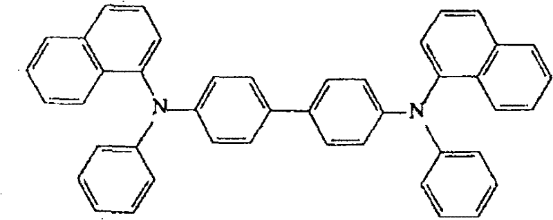
对于空穴传输层164的材料,优选包括三芳基胺化合物的材料。该材料可以以其离子能量位于空穴注入层与发光层之间的方式适当进行选择。例如,可以使用NPB(化学式1)。For the material of the
[化学式1][chemical formula 1]
发光层166是对传输的空穴和传输的电子进行复合的荧光发射层和/或磷光发射层。该发光层具有5nm-3000nm的膜厚dM,并且含有发光性色素和主体材料。The
只要该发光性色素的第一氧化电位(ED+)低于该主体材料的第一氧化电位(EH+),并且该发光性色素的第一还原电位(ED-)低于该主体材料的第一还原电位(EH-),就可以对该发光性色素和该主体材料适当进行选择以便满足特性。对于该发光性色素,优选下式(化学式2)表示的有机金属络合物,例如可以使用Ir(ppy)3(化学式3)。As long as the first oxidation potential (ED+) of the luminescent pigment is lower than the first oxidation potential (EH+) of the host material, and the first reduction potential (ED-) of the luminescent pigment is lower than the first reduction potential of the host material Potential (EH-), the luminescent dye and the host material can be appropriately selected so as to satisfy the characteristics. As the luminous dye, an organometallic complex represented by the following formula (Chemical formula 2) is preferable, for example, Ir(ppy) 3 (Chemical formula 3) can be used.
[化学式2][chemical formula 2]

在该式中,M表示金属并且m+n表示该金属的价数。对于金属,列举的是钌、铑、钯、银、铼、锇、铱、铂和金。m为不小于0的整数,并且n为不小于1的整数。L表示单价二齿配体。环a和环b表示可以具有取代基团的芳烃基团。In the formula, M represents a metal and m+n represents the valence of the metal. As metals, ruthenium, rhodium, palladium, silver, rhenium, osmium, iridium, platinum and gold are cited. m is an integer not smaller than 0, and n is an integer not smaller than 1. L represents a monovalent bidentate ligand. Ring a and ring b represent an aromatic hydrocarbon group which may have a substituent.
[化学式3][chemical formula 3]

对于主体材料,优选使用咔唑化合物和吡啶化合物中的至少一种化合物。或者可以使用咔唑化合物和吡啶化合物二者。对于主体材料,优选如下式(化学式4-6)所示的在同一分子中具有咔唑基团和吡啶环的化合物。For the host material, it is preferable to use at least one compound among carbazole compounds and pyridine compounds. Alternatively, both the carbazole compound and the pyridine compound may be used. As the host material, a compound having a carbazole group and a pyridine ring in the same molecule as shown in the following formula (Chemical Formula 4-6) is preferable.
[化学式4][chemical formula 4]

(Z表示直接结合、或能够使各咔唑环的氮原子之间共轭的任意连接基团)。(Z represents any linking group that is directly bonded or that can conjugate the nitrogen atoms of the respective carbazole rings).
Q表示连接到G上的直接结合。Q represents a direct bond attached to G.
B表示具有n个N原子作为杂原子的六元环的芳香族杂环。B represents a six-membered aromatic heterocyclic ring having n N atoms as heteroatoms.
n表示1-3的整数。n represents an integer of 1-3.
G在环B的N原子的邻位或对位与C原子结合。G is bonded to the C atom at the ortho or para position of the N atom of the ring B.
在与Q键合(linkage)的情况下,G表示直接结合或与Q连接的任意连接基团。In the case of linkage to Q, G represents any linking group directly bound or linked to Q.
在未与Q键合的情况下,G表示芳香烃基团。When not bonded to Q, G represents an aromatic hydrocarbon group.
m为3-5的整数。m is an integer of 3-5.
存在于分子中的多个G可以相同或不同。Multiple Gs present in the molecule may be the same or different.
环B可以具有除G以外的取代基。)Ring B may have substituents other than G. )
[化学式5][chemical formula 5]

(Z1和Z2表示直接结合或任意连接基团。(Z 1 and Z 2 represent direct bonding or any linking group.
Z1、Z2和环A可以具有取代基。Z 1 , Z 2 and ring A may have substituents.
Z1与Z2可以相同或不同。 Z1 and Z2 may be the same or different.
Q表示与G直接结合。Q indicates direct binding to G.
B为具有n个N原子作为杂原子的六元环的芳香族杂环。B is a six-membered aromatic heterocyclic ring having n N atoms as heteroatoms.
G在环B的N原子的邻位或对位与C原子结合。G is bonded to the C atom at the ortho or para position of the N atom of the ring B.
在与Q键合的情况下,G表示与Q直接结合或任意连接基团。In the case of bonding to Q, G represents a direct bond to Q or any linking group.
在未与Q键合的情况下,G表示芳香烃基团。When not bonded to Q, G represents an aromatic hydrocarbon group.
m为3-5的整数。m is an integer of 3-5.
存在于分子中的多个G可以相同或不同。Multiple Gs present in the molecule may be the same or different.
环B可以具有除G以外的取代基。)Ring B may have substituents other than G. )
[化学式6][chemical formula 6]

(Z1和Z2表示直接结合或任意连接基团。Z1与Z2可以相同或不同。(Z 1 and Z 2 represent direct bonding or any linking group. Z 1 and Z 2 may be the same or different.
环B1和环B2为吡啶环。Ring B 1 and Ring B 2 are pyridine rings.
Z1、Z2、环B1和环B2可以具有取代基。)Z 1 , Z 2 , ring B 1 and ring B 2 may have substituents. )
具体地,列举下述化合物。Specifically, the following compounds are listed.
[化学式7][chemical formula 7]

[化学式8][chemical formula 8]

[化学式9][chemical formula 9]

[化学式10][chemical formula 10]

[化学式11][chemical formula 11]

[化学式12][chemical formula 12]

电子传输层168提供在阴极18(若提供了电子注入层则为电子注入层)与发光层166之间,它是加速电子传输的层,具有将电子适当传输至发光层166的作用。电子传输层168的膜厚dE为5nm-3000nm,并且其与空穴传输层164的膜厚dH的关系要求设定为dH≤dE。进一步地,电子传输层168不限于单层并且可以由多层形成。在多层的情况下,与发光层166相邻的电子传输层形成为第一电子传输层,并且第一电子传输层由具有比电子传输层的其它组分更高的第一氧化电位的宽带隙的电子传输材料制成,以便促进将发光层中产生的激子限制在发光层中以提高效率。电子传输层的总数(NE;1-3)与空穴传输层的总数(NH;1-3)之间的关系优选设定为NH≤NE。The
在空穴传输层和/或电子传输层由多层形成的情况下,膜厚是指多层的总膜厚。In the case where the hole transport layer and/or the electron transport layer is formed of multiple layers, the film thickness refers to the total film thickness of the multiple layers.
对于电子传输层168的材料,优选包括有机铝络合物的材料。例如,可以使用Alq3(化学式13)、BAlq(化学式14),但材料不限于这些。For the material of the
[化学式13][chemical formula 13]

[化学式14][chemical formula 14]

发光性色素的第一氧化电位(ED+)、主体材料的第一氧化电位(EH+)、发光性色素的第一还原电位(ED-)、主体材料的第一还原电位(EH-)、电子传输层的材料的氧化还原电位可以通过电化学测量获得。The first oxidation potential (ED+) of the luminescent pigment, the first oxidation potential (EH+) of the host material, the first reduction potential (ED-) of the luminescent pigment, the first reduction potential (EH-) of the host material, electron transport The redox potential of the material of the layer can be obtained by electrochemical measurement.
下面解释电化学测量方法。将约0.1-2mM待测量的对象物质溶解在含有约0.1mol/L的高氯酸四丁基铵、六氟磷酸四丁基铵等作为支持电解质的有机溶剂中,并且将待测量对象物质在工作电极下进行氧化还原,该工作电极使用玻璃碳电极作为工作电极、铂电极作为电极对,以及银电极作为参比电极。待测量的对象物质的氧化还原电位通过比较这些电位与参比物质例如二茂铁的氧化还原电位进行计算。列举循环伏安法作为电化学测量方法。The electrochemical measurement method is explained below. Dissolve about 0.1-2mM object substance to be measured in an organic solvent containing about 0.1mol/L tetrabutylammonium perchlorate, tetrabutylammonium hexafluorophosphate, etc. as a supporting electrolyte, and place the object substance to be measured in Redox is carried out under the working electrode, which uses a glassy carbon electrode as the working electrode, a platinum electrode as the electrode pair, and a silver electrode as the reference electrode. The oxidation-reduction potential of the object substance to be measured is calculated by comparing these potentials with the oxidation-reduction potential of a reference substance such as ferrocene. Cyclic voltammetry is cited as electrochemical measuring method.
作为实例,通过上述方法测量的Ir(ppy)3、化学式4-9的化合物、Alq3和BAlq的氧化还原电位列于表1。As an example, the oxidation-reduction potentials of Ir(ppy) 3 , compounds of Chemical Formulas 4-9, Alq 3 and BAlq measured by the above method are listed in Table 1.
[表1][Table 1]
表1.各化合物的氧化还原电位Table 1. Redox potential of each compound
实施例Example
具体地,制备多个有机EL元件的样品并且评价工作寿命。在这些样品中,将以下材料顺次蒸镀在位于各基板之上的ITO(膜厚110nm)阳极之上以产生下述构造的有机EL元件200。Specifically, samples of a plurality of organic EL elements were prepared and the operating life was evaluated. In these samples, the following materials were sequentially vapor-deposited on an ITO (film thickness 110 nm) anode positioned on each substrate to produce an organic EL element 200 of the configuration described below.
通过将铜酞菁(CuPc)用于空穴注入层162(各20nm的膜厚)、将NPB用于空穴传输层164、将添加了6%的化学式3所表示的Ir(ppy)3作为发光性色素的主体材料化学式7的化合物用于发光层166并将Alq3用于电子传输层168,如图2所示层叠各有机层。此时,空穴传输层、发光层以及电子传输层的各膜厚各不相同,如表2所示。By using copper phthalocyanine (CuPc) for the hole injection layer 162 (each with a film thickness of 20 nm), and using NPB for the
元件样品1为本发明的实施例,元件样品2则为比较例。在各电子传输层上进一步蒸镀1nm膜厚的LiF作为电子注入层,在其上进一步层叠100nm膜厚的铝(Al)作为阴极以制造该有机EL元件。Component sample 1 is an example of the present invention, and component sample 2 is a comparative example. On each electron transport layer, LiF was further vapor-deposited with a film thickness of 1 nm as an electron injection layer, and aluminum (Al) with a film thickness of 100 nm was further laminated thereon as a cathode to manufacture this organic EL element.
以2.5mA/cm2的电流密度连续驱动上述元件样品,并且测量从测量开始时至亮度减小20%时所用的时间。从测量开始时至元件样品2(比较例)的亮度减小20%时所用的时间用1表示,并且测量结果与形成有机材料层的空穴传输层/发光层/电子传输层的膜厚一起示于表2。The above element sample was continuously driven at a current density of 2.5 mA/cm 2 , and the time taken from the start of the measurement to the time when the luminance decreased by 20% was measured. The time taken from the start of the measurement to the time when the luminance of the element sample 2 (comparative example) decreases by 20% is represented by 1, and the measurement results are together with the film thicknesses of the hole transport layer/light emitting layer/electron transport layer forming the organic material layer Shown in Table 2.
[表2][Table 2]
表2.元件样品的膜厚构造以及连续驱动测试结果Table 2. Film thickness structure and continuous driving test results of component samples

表2显示,在实施例的元件样品1中驱动寿命得以提高。Table 2 shows that the driving life was improved in the element sample 1 of the embodiment.
在其它实施例中,使用化学式8的化合物代替化学式7的化合物作为发光层的主体材料,并且除了表3所设定的膜厚之外,制备与上述实施例相似的元件样品3、4、5、6和7。元件样品3、4和5为本发明的实施例,元件样品6和7为比较例。In other embodiments, the compound of chemical formula 8 is used instead of the compound of chemical formula 7 as the host material of the light-emitting layer, and except for the film thickness set in Table 3, component samples 3, 4, and 5 similar to the above-mentioned embodiments are prepared , 6 and 7. Element samples 3, 4, and 5 are examples of the present invention, and element samples 6 and 7 are comparative examples.
以2.5mA/cm2的电流密度连续驱动上述元件样品,并且测量从测量开始时至亮度减小20%时所用的时间。从测量开始时至元件样品6(比较例)的亮度减小20%时所用的时间用1表示,并且测量结果与形成有机材料层的空穴传输层/发光层/电子传输层的膜厚一起示于表3。The above element sample was continuously driven at a current density of 2.5 mA/cm 2 , and the time taken from the start of the measurement to the time when the luminance decreased by 20% was measured. The time taken from the start of the measurement to the time when the luminance of the element sample 6 (comparative example) decreases by 20% is represented by 1, and the measurement results are together with the film thicknesses of the hole transport layer/light emitting layer/electron transport layer forming the organic material layer Shown in Table 3.
[表3][table 3]
表3.元件样品的膜厚构造以及连续驱动测试结果Table 3. Film thickness structure and continuous driving test results of component samples

表3显示,与比较例的元件样品6和7相比,实施例的元件样品3、4和5的驱动寿命得以提高。Table 3 shows that the driving life of the element samples 3, 4 and 5 of the example was improved compared with the element samples 6 and 7 of the comparative example.
在其它实施例中,制备了本发明实施例的元件样品8,该元件样品与上述实施例中的相同,但电子传输层由双层形成。使用BAlq用于与发光层166相邻的第一电子传输层,并且使用Alq3用于布置在第一电子传输层与电子注入层之间的第二电子传输层。In other examples, an element sample 8 of an example of the present invention was prepared which was the same as in the above-mentioned examples except that the electron transport layer was formed of a double layer. BAlq was used for the first electron transport layer adjacent to the
以2.5mA/cm2的电流密度连续驱动上述元件样品,并且测量从测量开始时至亮度减小20%时所用的时间。从测量开始时至元件样品7(比较例)的亮度减小20%所用的时间用1表示,并且测量结果与形成有机材料层的空穴传输层/发光层/电子传输层(第一电子传输层和第二电子传输层)的膜厚一起示于表4。The above element sample was continuously driven at a current density of 2.5 mA/cm 2 , and the time taken from the start of the measurement to the time when the luminance decreased by 20% was measured. The time taken for the luminance of the element sample 7 (comparative example) to decrease by 20% from the start of the measurement is represented by 1, and the measurement results are compared with the hole transport layer/light emitting layer/electron transport layer (first electron transport layer) forming the organic material layer. layer and the second electron transport layer) are shown in Table 4 together.
[表4][Table 4]
表4.元件样品的膜厚构造以及连续驱动测试结果Table 4. Film thickness structure and continuous driving test results of component samples

表4显示,与比较例的元件样品7相比,实施例的元件样品8的驱动寿命得以提高。Table 4 shows that, compared with element sample 7 of the comparative example, the driving life of the element sample 8 of the example was improved.
进一步地,在其它实施例中,使用添加了17重量%的作为电子受容性物质且由化学式16所表示的芳族硼化合物盐的、化学式15表示的含有芳族二胺的聚醚(重均分子量为26900)代替铜酞菁作为电子注入层(膜厚为30nm)。并且NPB用于空穴传输层,将添加了6重量%的作为发光性色素的Ir(ppy)3的主体材料化学式9的化合物用于发光层,并且将Alq3用于电子传输层以制备其膜厚设定为如表4所示的元件样品9和10。元件样品9为本发明的实施例,并且元件样品10为比较例。Further, in other examples, the aromatic diamine-containing polyether represented by Chemical Formula 15 (weight average molecular weight of 26900) instead of copper phthalocyanine as the electron injection layer (thickness of 30nm). And NPB was used for the hole transport layer, the compound of the host material Chemical Formula 9 of Ir(ppy) 3 as a luminescent pigment added by 6% by weight was used for the light emitting layer, and Alq 3 was used for the electron transport layer to prepare it The film thickness was set to
[化学式15][chemical formula 15]
[化学式16][chemical formula 16]

通过在ITO阳极上旋涂涂布溶液形成空穴注入层,在该涂布溶液中,2重量%的含有芳族二胺的聚醚以及0.4重量%的电子受容性物质溶解在苯甲酸乙酯中。The hole injection layer was formed by spin-coating a coating solution in which 2% by weight of polyether containing aromatic diamine and 0.4% by weight of electron-accepting substance dissolved in ethyl benzoate was applied on the ITO anode. middle.
以7mA/cm2的电流密度连续驱动上述元件样品,并且测量从测量开始时至亮度减小20%时所用的时间。从测量开始时至元件样品10(比较例)的亮度减小20%时所用的时间用1表示,并且测量结果与形成有机材料层的空穴传输层/发光层/电子传输层的膜厚一起示于表5。The above-mentioned element sample was continuously driven at a current density of 7 mA/cm 2 , and the time taken from the start of the measurement to the time when the luminance decreased by 20% was measured. The time taken from the start of the measurement until the luminance of the element sample 10 (comparative example) decreases by 20% is represented by 1, and the measurement results are together with the film thicknesses of the hole transport layer/light emitting layer/electron transport layer forming the organic material layer Shown in Table 5.
表5显示,与比较例的元件样品9相比,实施例的元件样品10的驱动寿命得以提高。Table 5 shows that the driving life of the
[表5][table 5]
表5.元件样品的膜厚构造以及连续驱动测试结果Table 5. Film thickness structure of component samples and continuous driving test results

因此,根据这些实施例可以获得具有长驱动寿命的有机EL元件。Therefore, according to these examples, an organic EL element having a long driving life can be obtained.
Claims (13)


Applications Claiming Priority (3)
| Application Number | Priority Date | Filing Date | Title |
|---|---|---|---|
| JP150747/2005 | 2005-05-24 | ||
| JP2005150747 | 2005-05-24 | ||
| PCT/JP2006/310254 WO2006126542A1 (en) | 2005-05-24 | 2006-05-23 | Organic electroluminescent device |
Publications (2)
| Publication Number | Publication Date |
|---|---|
| CN101185176A CN101185176A (en) | 2008-05-21 |
| CN101185176B true CN101185176B (en) | 2010-04-07 |
Family
ID=37451967
Family Applications (1)
| Application Number | Title | Priority Date | Filing Date |
|---|---|---|---|
| CN200680018350.4A Active CN101185176B (en) | 2005-05-24 | 2006-05-23 | organic electroluminescent element |
Country Status (7)
| Country | Link |
|---|---|
| US (1) | US8933622B2 (en) |
| EP (1) | EP1887640A4 (en) |
| JP (1) | JP5008557B2 (en) |
| KR (1) | KR101243833B1 (en) |
| CN (1) | CN101185176B (en) |
| TW (1) | TWI395509B (en) |
| WO (1) | WO2006126542A1 (en) |
Families Citing this family (30)
| Publication number | Priority date | Publication date | Assignee | Title |
|---|---|---|---|---|
| CN101076528B (en) * | 2004-12-10 | 2012-06-20 | 三菱化学株式会社 | Organic compounds, charge transport materials and organic electroluminescent devices |
| WO2006067976A1 (en) * | 2004-12-24 | 2006-06-29 | Pioneer Corporation | Organic compound, charge-transporting material, and organic electroluminescent element |
| CN101185176B (en) | 2005-05-24 | 2010-04-07 | 日本先锋公司 | organic electroluminescent element |
| US7651791B2 (en) | 2005-12-15 | 2010-01-26 | Idemitsu Kosan Co., Ltd. | Material for organic electroluminescence device and electroluminescence device employing the same |
| JPWO2008120355A1 (en) * | 2007-03-29 | 2010-07-15 | パイオニア株式会社 | Organic EL device |
| KR20120119100A (en) * | 2011-04-20 | 2012-10-30 | 삼성디스플레이 주식회사 | Organic light emitting device |
| KR102025031B1 (en) | 2011-11-22 | 2019-11-14 | 이데미쓰 고산 가부시키가이샤 | Aromatic heterocyclic derivative, material for organic electroluminescent element, and organic electroluminescent element |
| WO2014047616A1 (en) | 2012-09-24 | 2014-03-27 | Arizona Board Of Regents For And On Behalf Of Arizona State University | Metal compounds, methods, and uses thereof |
| US20150274762A1 (en) | 2012-10-26 | 2015-10-01 | Arizona Board Of Regents Acting For And On Behalf Of Arizona State University | Metal complexes, methods, and uses thereof |
| JP6804823B2 (en) | 2013-10-14 | 2020-12-23 | アリゾナ・ボード・オブ・リージェンツ・オン・ビハーフ・オブ・アリゾナ・ステイト・ユニバーシティーArizona Board of Regents on behalf of Arizona State University | Platinum complex and device |
| CN104370887B (en) | 2013-12-26 | 2016-08-24 | 北京阿格蕾雅科技发展有限公司 | Synthetic method of 2,6-bis[3-(N-carbazolyl)phenyl]pyridine compounds |
| US10020455B2 (en) | 2014-01-07 | 2018-07-10 | Arizona Board Of Regents On Behalf Of Arizona State University | Tetradentate platinum and palladium complex emitters containing phenyl-pyrazole and its analogues |
| US9941479B2 (en) | 2014-06-02 | 2018-04-10 | Arizona Board Of Regents On Behalf Of Arizona State University | Tetradentate cyclometalated platinum complexes containing 9,10-dihydroacridine and its analogues |
| US9923155B2 (en) | 2014-07-24 | 2018-03-20 | Arizona Board Of Regents On Behalf Of Arizona State University | Tetradentate platinum (II) complexes cyclometalated with functionalized phenyl carbene ligands and their analogues |
| WO2016025921A1 (en) | 2014-08-15 | 2016-02-18 | Arizona Board Of Regents On Behalf Of Arizona State University | Non-platinum metal complexes for excimer based single dopant white organic light emitting diodes |
| US10033003B2 (en) | 2014-11-10 | 2018-07-24 | Arizona Board Of Regents On Behalf Of Arizona State University | Tetradentate metal complexes with carbon group bridging ligands |
| US9879039B2 (en) | 2015-06-03 | 2018-01-30 | Arizona Board Of Regents On Behalf Of Arizona State University | Tetradentate and octahedral metal complexes containing naphthyridinocarbazole and its analogues |
| KR102002885B1 (en) * | 2016-11-25 | 2019-10-01 | 주식회사 엘지화학 | Coating composition and organic light emitting device |
| WO2018140765A1 (en) | 2017-01-27 | 2018-08-02 | Jian Li | Metal-assisted delayed fluorescent emitters employing pyrido-pyrrolo-acridine and analogues |
| US11101435B2 (en) | 2017-05-19 | 2021-08-24 | Arizona Board Of Regents On Behalf Of Arizona State University | Tetradentate platinum and palladium complexes based on biscarbazole and analogues |
| US10516117B2 (en) | 2017-05-19 | 2019-12-24 | Arizona Board Of Regents On Behalf Of Arizona State University | Metal-assisted delayed fluorescent emttters employing benzo-imidazo-phenanthridine and analogues |
| US11647643B2 (en) | 2017-10-17 | 2023-05-09 | Arizona Board Of Regents On Behalf Of Arizona State University | Hole-blocking materials for organic light emitting diodes |
| WO2019079508A2 (en) * | 2017-10-17 | 2019-04-25 | Jian Li | Phosphorescent excimers with preferred molecular orientation as monochromatic emitters for display and lighting applications |
| US12037348B2 (en) | 2018-03-09 | 2024-07-16 | Arizona Board Of Regents On Behalf Of Arizona State University | Blue and narrow band green and red emitting metal complexes |
| US11778904B2 (en) * | 2018-05-09 | 2023-10-03 | Kyulux, Inc. | Composition of matter for use in organic light-emitting diodes |
| KR20200023984A (en) | 2018-08-27 | 2020-03-06 | 삼성전자주식회사 | Heterocyclic compound and organic light emitting device including the same |
| US11878988B2 (en) | 2019-01-24 | 2024-01-23 | Arizona Board Of Regents On Behalf Of Arizona State University | Blue phosphorescent emitters employing functionalized imidazophenthridine and analogues |
| US11785838B2 (en) | 2019-10-02 | 2023-10-10 | Arizona Board Of Regents On Behalf Of Arizona State University | Green and red organic light-emitting diodes employing excimer emitters |
| CN113683625B (en) | 2020-05-19 | 2025-06-10 | 亚利桑那州立大学董事会 | Metal-assisted delayed fluorescence emitters for organic light emitting diodes |
| US11945985B2 (en) | 2020-05-19 | 2024-04-02 | Arizona Board Of Regents On Behalf Of Arizona State University | Metal assisted delayed fluorescent emitters for organic light-emitting diodes |
Citations (2)
| Publication number | Priority date | Publication date | Assignee | Title |
|---|---|---|---|---|
| JP2002056985A (en) * | 2000-05-29 | 2002-02-22 | Mitsubishi Chemicals Corp | Organic electroluminescent device and method of manufacturing the same |
| JP2004171828A (en) * | 2002-11-18 | 2004-06-17 | Idemitsu Kosan Co Ltd | Organic electroluminescence device |
Family Cites Families (50)
| Publication number | Priority date | Publication date | Assignee | Title |
|---|---|---|---|---|
| US7829A (en) * | 1850-12-10 | Machine foe | ||
| JPH04172357A (en) | 1990-11-05 | 1992-06-19 | Konica Corp | Electrophotographic sensitive body |
| JPH07110940B2 (en) | 1991-06-05 | 1995-11-29 | 住友化学工業株式会社 | Organic electroluminescent device |
| DE69204359T2 (en) | 1991-06-05 | 1996-04-18 | Sumitomo Chemical Co | Organic electroluminescent devices. |
| US5178215A (en) * | 1991-07-22 | 1993-01-12 | Folsom Metal Products, Inc. | Rotary blowout preventer adaptable for use with both kelly and overhead drive mechanisms |
| JPH0867872A (en) * | 1994-08-29 | 1996-03-12 | Pioneer Electron Corp | Organic electroluminescence element |
| US6274979B1 (en) * | 1997-09-17 | 2001-08-14 | Texas Instruments Incorporated | Organic light emitting diodes |
| JPH11251067A (en) * | 1998-03-02 | 1999-09-17 | Junji Kido | Organic electroluminescent device |
| KR100280707B1 (en) * | 1998-11-12 | 2001-02-01 | 김순택 | Light-Emitting Compound and Display Device Adopting It as Coloring Material |
| JP4320811B2 (en) * | 1998-12-07 | 2009-08-26 | コニカミノルタホールディングス株式会社 | Organic electroluminescence device |
| JP4006862B2 (en) | 1998-12-22 | 2007-11-14 | コニカミノルタホールディングス株式会社 | Novel amino compound, its production method and use |
| JP2001313178A (en) | 2000-04-28 | 2001-11-09 | Pioneer Electronic Corp | Organic electroluminescence device |
| US6645645B1 (en) * | 2000-05-30 | 2003-11-11 | The Trustees Of Princeton University | Phosphorescent organic light emitting devices |
| JP4558153B2 (en) * | 2000-07-27 | 2010-10-06 | 三星モバイルディスプレイ株式會社 | Organic electroluminescence device |
| JP4023204B2 (en) | 2001-05-02 | 2007-12-19 | 淳二 城戸 | Organic electroluminescence device |
| JP2003022893A (en) | 2001-07-06 | 2003-01-24 | Fuji Photo Film Co Ltd | Luminescent element |
| US6863997B2 (en) * | 2001-12-28 | 2005-03-08 | The Trustees Of Princeton University | White light emitting OLEDs from combined monomer and aggregate emission |
| CN1643105A (en) | 2002-03-15 | 2005-07-20 | 出光兴产株式会社 | Material for organic electroluminescent device and organic electroluminescent device prepared using the material |
| EP2169028B1 (en) | 2002-03-22 | 2018-11-21 | Idemitsu Kosan Co., Ltd. | Material for organic electroluminescent devices and organic electroluminescent devices made by using the same |
| TW200305632A (en) | 2002-03-25 | 2003-11-01 | Idemitsu Kosan Co | Material for organic electroluminescent element and organic electroluminescent element employing the same |
| JP3925265B2 (en) | 2002-03-25 | 2007-06-06 | コニカミノルタホールディングス株式会社 | Organic electroluminescence element and display device using the same |
| US6692846B2 (en) * | 2002-06-20 | 2004-02-17 | Eastman Kodak Company | Organic electroluminescent device having a stabilizing dopant in a hole-transport layer or in an electron-transport layer distant from the emission layer |
| JP4103491B2 (en) | 2002-08-07 | 2008-06-18 | コニカミノルタホールディングス株式会社 | Organic electroluminescence element and display device |
| JP4427947B2 (en) | 2002-11-18 | 2010-03-10 | コニカミノルタホールディングス株式会社 | Organic electroluminescence element and display device |
| JP4707082B2 (en) * | 2002-11-26 | 2011-06-22 | コニカミノルタホールディングス株式会社 | Organic electroluminescence element and display device |
| JP4590825B2 (en) * | 2003-02-21 | 2010-12-01 | コニカミノルタホールディングス株式会社 | White light emitting organic electroluminescence device |
| JP4552382B2 (en) | 2003-03-06 | 2010-09-29 | コニカミノルタホールディングス株式会社 | ORGANIC ELECTROLUMINESCENT ELEMENT, ORGANIC ELECTROLUMINESCENT ELEMENT MATERIAL, DISPLAY DEVICE AND LIGHTING DEVICE |
| JP2004311413A (en) * | 2003-03-26 | 2004-11-04 | Konica Minolta Holdings Inc | Organic electroluminescence element, display device and lighting device |
| US20040209115A1 (en) * | 2003-04-21 | 2004-10-21 | Thompson Mark E. | Organic light emitting devices with wide gap host materials |
| KR100527194B1 (en) * | 2003-06-24 | 2005-11-08 | 삼성에스디아이 주식회사 | organic electroluminescence device employing doped hole transfer layer and/or hole injection layer |
| JP4561221B2 (en) | 2003-07-31 | 2010-10-13 | 三菱化学株式会社 | Compound, charge transport material and organic electroluminescence device |
| JP4810805B2 (en) | 2003-07-31 | 2011-11-09 | 三菱化学株式会社 | Organic compound, charge transport material, organic electroluminescent element material, and organic electroluminescent element |
| EP1672961B1 (en) | 2003-07-31 | 2014-12-03 | Mitsubishi Chemical Corporation | Compound, charge transport material and organic electroluminescent device |
| JP4325324B2 (en) | 2003-09-10 | 2009-09-02 | コニカミノルタホールディングス株式会社 | Organic electroluminescence device |
| JP4369719B2 (en) * | 2003-10-03 | 2009-11-25 | 株式会社 日立ディスプレイズ | Organic EL display device |
| WO2005057987A1 (en) | 2003-12-15 | 2005-06-23 | Idemitsu Kosan Co., Ltd. | Material for organic electroluminescent device and organic electroluminescent device using same |
| JP2005203293A (en) * | 2004-01-19 | 2005-07-28 | Mitsubishi Chemicals Corp | Luminescent material and organic electroluminescent device |
| TWI428053B (en) | 2004-02-09 | 2014-02-21 | Idemitsu Kosan Co | Organic electroluminescent element |
| TW200541401A (en) | 2004-02-13 | 2005-12-16 | Idemitsu Kosan Co | Organic electroluminescent device |
| JPWO2005085387A1 (en) | 2004-03-08 | 2007-12-13 | 出光興産株式会社 | Material for organic electroluminescence device and organic electroluminescence device using the same |
| US7201986B2 (en) * | 2004-05-04 | 2007-04-10 | Angstrom Power Incorporated | Electrochemical cells formed on pleated substrates |
| CN101076528B (en) * | 2004-12-10 | 2012-06-20 | 三菱化学株式会社 | Organic compounds, charge transport materials and organic electroluminescent devices |
| WO2006067976A1 (en) | 2004-12-24 | 2006-06-29 | Pioneer Corporation | Organic compound, charge-transporting material, and organic electroluminescent element |
| EP1858094B1 (en) * | 2005-01-25 | 2017-03-08 | Pioneer Corporation | Organic compound, charge transport material and organic electroluminescent device |
| WO2006095539A1 (en) | 2005-02-21 | 2006-09-14 | Mitsubishi Chemical Corporation | Organic electric field light emitting element and production therefor |
| JP5261887B2 (en) | 2005-05-17 | 2013-08-14 | 三菱化学株式会社 | Monoamine compound, charge transport material, and organic electroluminescence device |
| CN101185176B (en) | 2005-05-24 | 2010-04-07 | 日本先锋公司 | organic electroluminescent element |
| US8592052B2 (en) * | 2005-12-16 | 2013-11-26 | Mitsubishi Chemical Corporation | Organic electroluminescence device |
| WO2007069740A1 (en) * | 2005-12-16 | 2007-06-21 | Pioneer Corporation | Organic electroluminescent device |
| KR100964225B1 (en) * | 2008-03-19 | 2010-06-17 | 삼성모바일디스플레이주식회사 | Organic light emitting display device |
-
2006
- 2006-05-23 CN CN200680018350.4A patent/CN101185176B/en active Active
- 2006-05-23 EP EP06746738A patent/EP1887640A4/en not_active Withdrawn
- 2006-05-23 KR KR1020077029804A patent/KR101243833B1/en not_active Expired - Fee Related
- 2006-05-23 US US11/915,348 patent/US8933622B2/en active Active
- 2006-05-23 JP JP2007517841A patent/JP5008557B2/en not_active Expired - Fee Related
- 2006-05-23 WO PCT/JP2006/310254 patent/WO2006126542A1/en not_active Ceased
- 2006-05-24 TW TW095118392A patent/TWI395509B/en not_active IP Right Cessation
Patent Citations (2)
| Publication number | Priority date | Publication date | Assignee | Title |
|---|---|---|---|---|
| JP2002056985A (en) * | 2000-05-29 | 2002-02-22 | Mitsubishi Chemicals Corp | Organic electroluminescent device and method of manufacturing the same |
| JP2004171828A (en) * | 2002-11-18 | 2004-06-17 | Idemitsu Kosan Co Ltd | Organic electroluminescence device |
Non-Patent Citations (2)
| Title |
|---|
| 黄春辉.光电功能超薄膜 第1版.北京大学出版社,2001,第286-287页. * |
| 黄春辉.光电功能超薄膜第1版.北京大学出版社,2001,第286-287页. * |
Also Published As
| Publication number | Publication date |
|---|---|
| EP1887640A1 (en) | 2008-02-13 |
| US20090134779A1 (en) | 2009-05-28 |
| JPWO2006126542A1 (en) | 2008-12-25 |
| WO2006126542A1 (en) | 2006-11-30 |
| KR20080025073A (en) | 2008-03-19 |
| EP1887640A4 (en) | 2012-04-04 |
| TW200706062A (en) | 2007-02-01 |
| CN101185176A (en) | 2008-05-21 |
| US8933622B2 (en) | 2015-01-13 |
| KR101243833B1 (en) | 2013-03-20 |
| TWI395509B (en) | 2013-05-01 |
| JP5008557B2 (en) | 2012-08-22 |
Similar Documents
| Publication | Publication Date | Title |
|---|---|---|
| CN101185176B (en) | organic electroluminescent element | |
| KR102551368B1 (en) | Light-emitting element | |
| JP5384789B2 (en) | Organic light-emitting devices using binuclear metal compounds as light-emitting materials | |
| JP5328356B2 (en) | Electron blocking layer for highly efficient phosphorescent organic light-emitting devices | |
| US7598381B2 (en) | Near-infrared emitting organic compounds and organic devices using the same | |
| US20210135142A1 (en) | Organic electroluminescent device based on exciplex and excimer system | |
| US8778511B2 (en) | OLED stability via doped hole transport layer | |
| JP5624459B2 (en) | Organic electroluminescence device | |
| US20040209116A1 (en) | Organic light emitting devices with wide gap host materials | |
| US20100032626A1 (en) | Benzimidazole compound-containing composition and light-emitting device using the composition | |
| KR20110136885A (en) | Organic electroluminescent devices | |
| CN101371377A (en) | Organic electroluminescent device | |
| US8592052B2 (en) | Organic electroluminescence device | |
| TWI422273B (en) | Organic electric field light-emitting element | |
| JPWO2008120355A1 (en) | Organic EL device | |
| JP4823601B2 (en) | Polymer light emitting material, organic electroluminescence element, and display device | |
| CN100561768C (en) | Organic Electroluminescent Devices | |
| JP6503699B2 (en) | Organic electroluminescent device, method of manufacturing the same, and organic electroluminescent lighting device | |
| JP5078487B2 (en) | Electroluminescent device material and electroluminescent device using the same | |
| JP6492565B2 (en) | Method of manufacturing organic electroluminescent device, and method of manufacturing organic electroluminescent lighting device |
Legal Events
| Date | Code | Title | Description |
|---|---|---|---|
| C06 | Publication | ||
| PB01 | Publication | ||
| C10 | Entry into substantive examination | ||
| SE01 | Entry into force of request for substantive examination | ||
| C14 | Grant of patent or utility model | ||
| GR01 | Patent grant | ||
| CP01 | Change in the name or title of a patent holder | ||
| CP01 | Change in the name or title of a patent holder |
Address after: Tokyo, Japan Co-patentee after: MITSUBISHI CHEMICAL Corp. Patentee after: PIONEER Corp. Address before: Tokyo, Japan Co-patentee before: MITSUBISHI RAYON Co.,Ltd. Patentee before: PIONEER Corp. |
|
| TR01 | Transfer of patent right | ||
| TR01 | Transfer of patent right |
Effective date of registration: 20170912 Address after: Tokyo, Japan Co-patentee after: MITSUBISHI RAYON Co.,Ltd. Patentee after: PIONEER Corp. Address before: Tokyo, Japan Co-patentee before: MITSUBISHI CHEMICAL Corp. Patentee before: PIONEER Corp. |