CN101166394A - Multilayer wiring board mounted with electronic components and manufacturing method thereof - Google Patents
Multilayer wiring board mounted with electronic components and manufacturing method thereof Download PDFInfo
- Publication number
- CN101166394A CN101166394A CNA2007101632526A CN200710163252A CN101166394A CN 101166394 A CN101166394 A CN 101166394A CN A2007101632526 A CNA2007101632526 A CN A2007101632526A CN 200710163252 A CN200710163252 A CN 200710163252A CN 101166394 A CN101166394 A CN 101166394A
- Authority
- CN
- China
- Prior art keywords
- electronic component
- opening
- wiring board
- copper foil
- layer
- Prior art date
- Legal status (The legal status is an assumption and is not a legal conclusion. Google has not performed a legal analysis and makes no representation as to the accuracy of the status listed.)
- Pending
Links
Images


Classifications
-
- H—ELECTRICITY
- H05—ELECTRIC TECHNIQUES NOT OTHERWISE PROVIDED FOR
- H05K—PRINTED CIRCUITS; CASINGS OR CONSTRUCTIONAL DETAILS OF ELECTRIC APPARATUS; MANUFACTURE OF ASSEMBLAGES OF ELECTRICAL COMPONENTS
- H05K3/00—Apparatus or processes for manufacturing printed circuits
- H05K3/46—Manufacturing multilayer circuits
-
- H—ELECTRICITY
- H05—ELECTRIC TECHNIQUES NOT OTHERWISE PROVIDED FOR
- H05K—PRINTED CIRCUITS; CASINGS OR CONSTRUCTIONAL DETAILS OF ELECTRIC APPARATUS; MANUFACTURE OF ASSEMBLAGES OF ELECTRICAL COMPONENTS
- H05K1/00—Printed circuits
- H05K1/18—Printed circuits structurally associated with non-printed electric components
- H05K1/182—Printed circuits structurally associated with non-printed electric components associated with components mounted in printed circuit boards [PCB], e.g. insert-mounted components [IMC]
- H05K1/185—Printed circuits structurally associated with non-printed electric components associated with components mounted in printed circuit boards [PCB], e.g. insert-mounted components [IMC] associated with components encapsulated in the insulating substrate of the PCBs; associated with components incorporated in internal layers of multilayer circuit boards
- H05K1/186—Printed circuits structurally associated with non-printed electric components associated with components mounted in printed circuit boards [PCB], e.g. insert-mounted components [IMC] associated with components encapsulated in the insulating substrate of the PCBs; associated with components incorporated in internal layers of multilayer circuit boards manufactured by mounting on or connecting to patterned circuits before or during embedding
-
- H—ELECTRICITY
- H10—SEMICONDUCTOR DEVICES; ELECTRIC SOLID-STATE DEVICES NOT OTHERWISE PROVIDED FOR
- H10W—GENERIC PACKAGES, INTERCONNECTIONS, CONNECTORS OR OTHER CONSTRUCTIONAL DETAILS OF DEVICES COVERED BY CLASS H10
- H10W70/00—Package substrates; Interposers; Redistribution layers [RDL]
- H10W70/60—Insulating or insulated package substrates; Interposers; Redistribution layers
- H10W70/611—Insulating or insulated package substrates; Interposers; Redistribution layers for connecting multiple chips together
- H10W70/614—Insulating or insulated package substrates; Interposers; Redistribution layers for connecting multiple chips together the multiple chips being integrally enclosed
-
- H—ELECTRICITY
- H10—SEMICONDUCTOR DEVICES; ELECTRIC SOLID-STATE DEVICES NOT OTHERWISE PROVIDED FOR
- H10W—GENERIC PACKAGES, INTERCONNECTIONS, CONNECTORS OR OTHER CONSTRUCTIONAL DETAILS OF DEVICES COVERED BY CLASS H10
- H10W70/00—Package substrates; Interposers; Redistribution layers [RDL]
- H10W70/60—Insulating or insulated package substrates; Interposers; Redistribution layers
- H10W70/67—Insulating or insulated package substrates; Interposers; Redistribution layers characterised by their insulating layers or insulating parts
- H10W70/68—Shapes or dispositions thereof
- H10W70/685—Shapes or dispositions thereof comprising multiple insulating layers
-
- H—ELECTRICITY
- H05—ELECTRIC TECHNIQUES NOT OTHERWISE PROVIDED FOR
- H05K—PRINTED CIRCUITS; CASINGS OR CONSTRUCTIONAL DETAILS OF ELECTRIC APPARATUS; MANUFACTURE OF ASSEMBLAGES OF ELECTRICAL COMPONENTS
- H05K2201/00—Indexing scheme relating to printed circuits covered by H05K1/00
- H05K2201/09—Shape and layout
- H05K2201/09818—Shape or layout details not covered by a single group of H05K2201/09009 - H05K2201/09809
- H05K2201/09845—Stepped hole, via, edge, bump or conductor
-
- H—ELECTRICITY
- H05—ELECTRIC TECHNIQUES NOT OTHERWISE PROVIDED FOR
- H05K—PRINTED CIRCUITS; CASINGS OR CONSTRUCTIONAL DETAILS OF ELECTRIC APPARATUS; MANUFACTURE OF ASSEMBLAGES OF ELECTRICAL COMPONENTS
- H05K2203/00—Indexing scheme relating to apparatus or processes for manufacturing printed circuits covered by H05K3/00
- H05K2203/04—Soldering or other types of metallurgic bonding
- H05K2203/049—Wire bonding
-
- H—ELECTRICITY
- H05—ELECTRIC TECHNIQUES NOT OTHERWISE PROVIDED FOR
- H05K—PRINTED CIRCUITS; CASINGS OR CONSTRUCTIONAL DETAILS OF ELECTRIC APPARATUS; MANUFACTURE OF ASSEMBLAGES OF ELECTRICAL COMPONENTS
- H05K3/00—Apparatus or processes for manufacturing printed circuits
- H05K3/46—Manufacturing multilayer circuits
- H05K3/4602—Manufacturing multilayer circuits characterized by a special circuit board as base or central core whereon additional circuit layers are built or additional circuit boards are laminated
-
- H—ELECTRICITY
- H10—SEMICONDUCTOR DEVICES; ELECTRIC SOLID-STATE DEVICES NOT OTHERWISE PROVIDED FOR
- H10W—GENERIC PACKAGES, INTERCONNECTIONS, CONNECTORS OR OTHER CONSTRUCTIONAL DETAILS OF DEVICES COVERED BY CLASS H10
- H10W70/00—Package substrates; Interposers; Redistribution layers [RDL]
- H10W70/60—Insulating or insulated package substrates; Interposers; Redistribution layers
- H10W70/67—Insulating or insulated package substrates; Interposers; Redistribution layers characterised by their insulating layers or insulating parts
- H10W70/68—Shapes or dispositions thereof
- H10W70/682—Shapes or dispositions thereof comprising holes having chips therein
-
- H—ELECTRICITY
- H10—SEMICONDUCTOR DEVICES; ELECTRIC SOLID-STATE DEVICES NOT OTHERWISE PROVIDED FOR
- H10W—GENERIC PACKAGES, INTERCONNECTIONS, CONNECTORS OR OTHER CONSTRUCTIONAL DETAILS OF DEVICES COVERED BY CLASS H10
- H10W72/00—Interconnections or connectors in packages
- H10W72/50—Bond wires
- H10W72/551—Materials of bond wires
- H10W72/552—Materials of bond wires comprising metals or metalloids, e.g. silver
- H10W72/5522—Materials of bond wires comprising metals or metalloids, e.g. silver comprising gold [Au]
-
- H—ELECTRICITY
- H10—SEMICONDUCTOR DEVICES; ELECTRIC SOLID-STATE DEVICES NOT OTHERWISE PROVIDED FOR
- H10W—GENERIC PACKAGES, INTERCONNECTIONS, CONNECTORS OR OTHER CONSTRUCTIONAL DETAILS OF DEVICES COVERED BY CLASS H10
- H10W72/00—Interconnections or connectors in packages
- H10W72/50—Bond wires
- H10W72/551—Materials of bond wires
- H10W72/552—Materials of bond wires comprising metals or metalloids, e.g. silver
- H10W72/5524—Materials of bond wires comprising metals or metalloids, e.g. silver comprising aluminium [Al]
-
- H—ELECTRICITY
- H10—SEMICONDUCTOR DEVICES; ELECTRIC SOLID-STATE DEVICES NOT OTHERWISE PROVIDED FOR
- H10W—GENERIC PACKAGES, INTERCONNECTIONS, CONNECTORS OR OTHER CONSTRUCTIONAL DETAILS OF DEVICES COVERED BY CLASS H10
- H10W72/00—Interconnections or connectors in packages
- H10W72/50—Bond wires
- H10W72/551—Materials of bond wires
- H10W72/552—Materials of bond wires comprising metals or metalloids, e.g. silver
- H10W72/5525—Materials of bond wires comprising metals or metalloids, e.g. silver comprising copper [Cu]
-
- H—ELECTRICITY
- H10—SEMICONDUCTOR DEVICES; ELECTRIC SOLID-STATE DEVICES NOT OTHERWISE PROVIDED FOR
- H10W—GENERIC PACKAGES, INTERCONNECTIONS, CONNECTORS OR OTHER CONSTRUCTIONAL DETAILS OF DEVICES COVERED BY CLASS H10
- H10W72/00—Interconnections or connectors in packages
- H10W72/851—Dispositions of multiple connectors or interconnections
- H10W72/874—On different surfaces
- H10W72/877—Bump connectors and die-attach connectors
-
- H—ELECTRICITY
- H10—SEMICONDUCTOR DEVICES; ELECTRIC SOLID-STATE DEVICES NOT OTHERWISE PROVIDED FOR
- H10W—GENERIC PACKAGES, INTERCONNECTIONS, CONNECTORS OR OTHER CONSTRUCTIONAL DETAILS OF DEVICES COVERED BY CLASS H10
- H10W72/00—Interconnections or connectors in packages
- H10W72/851—Dispositions of multiple connectors or interconnections
- H10W72/874—On different surfaces
- H10W72/884—Die-attach connectors and bond wires
-
- H—ELECTRICITY
- H10—SEMICONDUCTOR DEVICES; ELECTRIC SOLID-STATE DEVICES NOT OTHERWISE PROVIDED FOR
- H10W—GENERIC PACKAGES, INTERCONNECTIONS, CONNECTORS OR OTHER CONSTRUCTIONAL DETAILS OF DEVICES COVERED BY CLASS H10
- H10W74/00—Encapsulations, e.g. protective coatings
-
- H—ELECTRICITY
- H10—SEMICONDUCTOR DEVICES; ELECTRIC SOLID-STATE DEVICES NOT OTHERWISE PROVIDED FOR
- H10W—GENERIC PACKAGES, INTERCONNECTIONS, CONNECTORS OR OTHER CONSTRUCTIONAL DETAILS OF DEVICES COVERED BY CLASS H10
- H10W74/00—Encapsulations, e.g. protective coatings
- H10W74/10—Encapsulations, e.g. protective coatings characterised by their shape or disposition
- H10W74/15—Encapsulations, e.g. protective coatings characterised by their shape or disposition on active surfaces of flip-chip devices, e.g. underfills
-
- H—ELECTRICITY
- H10—SEMICONDUCTOR DEVICES; ELECTRIC SOLID-STATE DEVICES NOT OTHERWISE PROVIDED FOR
- H10W—GENERIC PACKAGES, INTERCONNECTIONS, CONNECTORS OR OTHER CONSTRUCTIONAL DETAILS OF DEVICES COVERED BY CLASS H10
- H10W90/00—Package configurations
- H10W90/701—Package configurations characterised by the relative positions of pads or connectors relative to package parts
- H10W90/721—Package configurations characterised by the relative positions of pads or connectors relative to package parts of bump connectors
- H10W90/724—Package configurations characterised by the relative positions of pads or connectors relative to package parts of bump connectors between a chip and a stacked insulating package substrate, interposer or RDL
-
- H—ELECTRICITY
- H10—SEMICONDUCTOR DEVICES; ELECTRIC SOLID-STATE DEVICES NOT OTHERWISE PROVIDED FOR
- H10W—GENERIC PACKAGES, INTERCONNECTIONS, CONNECTORS OR OTHER CONSTRUCTIONAL DETAILS OF DEVICES COVERED BY CLASS H10
- H10W90/00—Package configurations
- H10W90/701—Package configurations characterised by the relative positions of pads or connectors relative to package parts
- H10W90/731—Package configurations characterised by the relative positions of pads or connectors relative to package parts of die-attach connectors
- H10W90/732—Package configurations characterised by the relative positions of pads or connectors relative to package parts of die-attach connectors between stacked chips
-
- H—ELECTRICITY
- H10—SEMICONDUCTOR DEVICES; ELECTRIC SOLID-STATE DEVICES NOT OTHERWISE PROVIDED FOR
- H10W—GENERIC PACKAGES, INTERCONNECTIONS, CONNECTORS OR OTHER CONSTRUCTIONAL DETAILS OF DEVICES COVERED BY CLASS H10
- H10W90/00—Package configurations
- H10W90/701—Package configurations characterised by the relative positions of pads or connectors relative to package parts
- H10W90/731—Package configurations characterised by the relative positions of pads or connectors relative to package parts of die-attach connectors
- H10W90/734—Package configurations characterised by the relative positions of pads or connectors relative to package parts of die-attach connectors between a chip and a stacked insulating package substrate, interposer or RDL
-
- H—ELECTRICITY
- H10—SEMICONDUCTOR DEVICES; ELECTRIC SOLID-STATE DEVICES NOT OTHERWISE PROVIDED FOR
- H10W—GENERIC PACKAGES, INTERCONNECTIONS, CONNECTORS OR OTHER CONSTRUCTIONAL DETAILS OF DEVICES COVERED BY CLASS H10
- H10W90/00—Package configurations
- H10W90/701—Package configurations characterised by the relative positions of pads or connectors relative to package parts
- H10W90/731—Package configurations characterised by the relative positions of pads or connectors relative to package parts of die-attach connectors
- H10W90/736—Package configurations characterised by the relative positions of pads or connectors relative to package parts of die-attach connectors between a chip and a stacked lead frame, conducting package substrate or heat sink
-
- H—ELECTRICITY
- H10—SEMICONDUCTOR DEVICES; ELECTRIC SOLID-STATE DEVICES NOT OTHERWISE PROVIDED FOR
- H10W—GENERIC PACKAGES, INTERCONNECTIONS, CONNECTORS OR OTHER CONSTRUCTIONAL DETAILS OF DEVICES COVERED BY CLASS H10
- H10W90/00—Package configurations
- H10W90/701—Package configurations characterised by the relative positions of pads or connectors relative to package parts
- H10W90/751—Package configurations characterised by the relative positions of pads or connectors relative to package parts of bond wires
- H10W90/754—Package configurations characterised by the relative positions of pads or connectors relative to package parts of bond wires between a chip and a stacked insulating package substrate, interposer or RDL
Landscapes
- Engineering & Computer Science (AREA)
- Manufacturing & Machinery (AREA)
- Microelectronics & Electronic Packaging (AREA)
- Production Of Multi-Layered Print Wiring Board (AREA)
Abstract
本发明公开了一种安装有电子元件的多层配线基板,该多层配线基板包括:电子元件;芯材层,其具有用于容纳所述电子元件的第一开口;树脂层,其形成在所述芯材层的一个表面上并具有大于所述第一开口的第二开口;支撑层,其形成在所述芯材层的另一表面上并支撑所述电子元件;多个连接导体部分,其在所述芯材层的所述一个表面上设置在所述第一开口周围并位于所述第二开口之内;结合引线,其用于将所述电子元件与所述连接导体部分电气连接;以及密封树脂,其填充入所述第一和第二开口,以密封所述电子元件和所述结合引线。
The invention discloses a multi-layer wiring substrate mounted with electronic components. The multi-layer wiring substrate comprises: an electronic component; a core material layer having a first opening for accommodating the electronic component; a resin layer comprising: formed on one surface of the core material layer and having a second opening larger than the first opening; a support layer formed on the other surface of the core material layer and supporting the electronic component; a plurality of connections a conductor portion provided on the one surface of the core material layer around the first opening and within the second opening; a bonding wire for connecting the electronic component to the connection conductor a portion of the electrical connection; and a sealing resin filled into the first and second openings to seal the electronic component and the bonding wire.
Description
技术领域technical field
本发明涉及一种安装有电子元件的多层配线基板以及用于制造该基板的方法。具体而言,本发明涉及一种安装有如下电子元件的多层配线基板,其中电子元件的多个电极端子与基板主体的多个连接导体部分通过引线结合彼此连接在一起,并且本发明还涉及用于制造该基板的方法。The present invention relates to a multilayer wiring substrate mounted with electronic components and a method for manufacturing the substrate. Specifically, the present invention relates to a multilayer wiring substrate mounted with electronic components in which a plurality of electrode terminals of the electronic component and a plurality of connecting conductor portions of the substrate main body are connected to each other by wire bonding, and the present invention also relates to It relates to a method for manufacturing the substrate.
背景技术Background technique
迄今为止,诸如结合以下专利文献1至3所述的配线基板等配线基板是已知的具有内置式电子元件(诸如半导体元件等)的配线基板。然而,关于现有技术的具有内置式电子元件的配线基板,尚未公开过如下构造,即:适当地内置通过引线结合连接到配线图案上的电子元件的构造。Hitherto, wiring substrates such as those described in conjunction with the following
可将专利文献1至3所述的技术作为与本发明相关的现有技术。专利文献1(未经审查的日本专利公开No.11-126978)说明了这样一种多层配线基板:即,在该多层配线基板上安装有诸如半导体元件、电容器以及电阻元件等的电气元件,并且可实现小型化、可提高电气元件的封装密度并增大配线电路层的密度。根据专利文献1,多层配线基板包括:绝缘基板,在该绝缘基板中堆叠有多个包含热固性树脂的绝缘层;多个配线电路层,其在绝缘基板上及内部形成;以及过孔导体(via hole conductor),其通过填充金属粉末而形成并用于使各半导体层相互连接。在该多层配线基板中,通过在绝缘基板中形成空腔并在该空腔中容纳电子元件从而形成配线芯板。然后,根据增层法,以贴装的方式在配线芯板的表面上依次堆叠含有感光树脂的绝缘层以及通过薄膜成形法制成的配线电路层。The techniques described in
专利文献2(未经审查的日本专利公开No.2001-313474)公开了这样一种配线基板:即,该配线基板经由树脂将电子元件内置在配线基板主体中,并且在不导致树脂或配线基板破裂或破损的情况下可以稳定而可靠地建立电子元件与内部配线层之间的导电性。在专利文献2中,设置有贯穿配线基板主体的通孔以及经由配线层堆叠在基板主体的前后表面上的绝缘层。在形成将要内置在通孔中并经由树脂固定的电子元件时,以满足关系a3<a1≤a2的方式设定配线基板主体的热膨胀系数(a1)、树脂的热膨胀系数(a2)以及电子元件的热膨胀系数(a3)。Patent Document 2 (Unexamined Japanese Patent Laid-Open No. 2001-313474) discloses a wiring substrate in which electronic components are built in a wiring substrate main body via a resin and without causing the resin to Or in the case of a crack or breakage of the wiring substrate, the electrical conductivity between the electronic component and the internal wiring layer can be established stably and reliably. In Patent Document 2, through holes penetrating through the wiring substrate main body and insulating layers stacked on the front and rear surfaces of the substrate main body via wiring layers are provided. When forming an electronic component to be built into a through hole and fixed via a resin, the thermal expansion coefficient (a1) of the wiring board main body (a1), the thermal expansion coefficient (a2) of the resin, and the electronic component are set so that the relationship a3<a1≤a2 is satisfied. The coefficient of thermal expansion (a3).
专利文献3(未经审查的日本专利公开No.2005-45013)说明了这样一种电路组件:即,该电路组件采用了空腔结构并可实现更高密度的封装、更高速度的操作以及更高频率的操作。在专利文献3中,该电路组件具有由陶瓷多层基板和树脂配线基板形成的结构。在陶瓷多层基板中,电子元件安装在空腔中,电子元件与空腔之间的间隙由热固性树脂填充,并将该陶瓷多层基板的表面制成平滑的。在树脂配线基板中,在绝缘粘合层中形成开口并将导电树脂填充入该开口中。树脂基板与陶瓷多层基板通过绝缘粘合层结合在一起,并且陶瓷多层基板上的上配线层与导电树脂电气连接在一起。Patent Document 3 (Unexamined Japanese Patent Laid-Open No. 2005-45013) describes a circuit assembly that employs a cavity structure and enables higher density packaging, higher speed operation, and higher frequency operation. In Patent Document 3, the circuit assembly has a structure formed of a ceramic multilayer substrate and a resin wiring substrate. In the ceramic multilayer substrate, electronic components are mounted in the cavity, the gap between the electronic component and the cavity is filled with a thermosetting resin, and the surface of the ceramic multilayer substrate is made smooth. In the resin wiring substrate, an opening is formed in the insulating adhesive layer and a conductive resin is filled into the opening. The resin substrate and the ceramic multilayer substrate are bonded together through an insulating adhesive layer, and the upper wiring layer on the ceramic multilayer substrate is electrically connected together with the conductive resin.
如上所述,在电子元件与配线基板主体通过引线结合电气连接在一起的现有技术的配线基板中,利用引线结合在电子元件与基板之间的引线呈环形。因此,要求密封部分等具有可以容纳该环的厚度,这样转而会阻碍在形成组件基板的过程中实现组件基板的小型化。As described above, in the related art wiring board in which the electronic component and the wiring board main body are electrically connected together by wire bonding, the lead wire between the electronic component and the substrate by wire bonding has a ring shape. Therefore, the sealing portion or the like is required to have a thickness capable of accommodating the ring, which in turn hinders miniaturization of the component substrate in the process of forming the component substrate.
而且,所形成的树脂密封材料层的表面具有低的平滑度,在该密封材料层上安装诸如表面安装器件等的电子元件是不可行的。Also, the surface of the formed resin encapsulant layer has low smoothness, and it is not feasible to mount electronic components such as surface mount devices on the encapsulant layer.
在专利文献1至3中的任一文献中,就降低多层基板的厚度、防止由于各种材料的热膨胀系数差异造成的基板变形等方面而言,已经设计出安装有电子元件的多层配线基板。然而,对于如下多层配线基板:即,其中电子元件安装在配线基板上并且电子元件与基板上用于连接的导体部分(在下文中称为“连接导体部分”)通过引线结合电气连接在一起,尚未公开过可实现显著降低厚度的多层配线基板。In any of
发明内容Contents of the invention
本发明的示例性实施例提供了一种多层配线基板,即使在通过引线结合将电子元件电气连接到配线基板主体上而形成所述多层配线基板的情况下,所述多层配线基板也可实现在所述配线基板主体中适当地内置所述电子元件并且可以具有减少的厚度。Exemplary embodiments of the present invention provide a multilayer wiring board even in the case where the multilayer wiring board is formed by electrically connecting electronic components to a wiring board main body by wire bonding, the multilayer wiring board The wiring substrate can also achieve proper incorporation of the electronic components in the wiring substrate main body and can have a reduced thickness.
根据本发明的一个或多个实施例,一种安装有电子元件的多层配线基板包括:电子元件;芯材层,其具有用于容纳所述电子元件的第一开口;树脂层,其形成在所述芯材层的一个表面上并具有大于所述第一开口的第二开口;多个连接导体部分,其在所述芯材层的所述一个表面上设置于所述第一开口周围并位于所述第二开口之内;结合引线,其用于将所述电子元件与所述连接导体部分电气连接;密封树脂,其填充入所述第一和第二开口,以密封所述电子元件和所述结合引线;以及配线图案,其形成在所述密封树脂上。According to one or more embodiments of the present invention, a multilayer wiring substrate mounted with electronic components includes: an electronic component; a core material layer having a first opening for accommodating the electronic component; a resin layer, which formed on one surface of the core material layer and having a second opening larger than the first opening; a plurality of connecting conductor portions disposed on the first opening on the one surface of the core material layer around and within the second opening; bonding wires for electrically connecting the electronic components with the connection conductor portion; sealing resin filled into the first and second openings to seal the An electronic component and the bonding wire; and a wiring pattern formed on the sealing resin.
如上所述,根据安装有电子元件的所述多层配线基板,诸如集成电路等电子元件容纳在芯材层的第一开口中。通过引线结合并利用树脂层的第二开口将电子元件电气连接到连接导体部分上。因此,与将电子元件直接安装在芯材层的上表面上并通过引线结合进行连接的情况相比,可以显著地减少安装有电子元件的多层配线基板的厚度,由此可形成薄的组件基板。As described above, according to the multilayer wiring substrate mounted with electronic components, electronic components such as integrated circuits are housed in the first openings of the core material layer. The electronic component is electrically connected to the connection conductor portion by wire bonding using the second opening of the resin layer. Therefore, compared with the case where the electronic components are directly mounted on the upper surface of the core material layer and connected by wire bonding, the thickness of the multilayer wiring substrate mounted with the electronic components can be significantly reduced, whereby a thin component substrate.
安装有电子元件的所述多层配线基板还可包括第二树脂层,所述第二树脂层形成在所述芯材层的另一表面上并具有第三开口,所述第三开口与所述第一开口的尺寸相同并与所述第一开口对准,其中所述电子元件容纳在由所述第一和第三开口形成的开口中。The multilayer wiring substrate mounted with electronic components may further include a second resin layer formed on the other surface of the core material layer and having a third opening that is connected to the other surface of the core material layer. The first openings are the same size and aligned with the first opening, wherein the electronic component is received in the opening formed by the first and third openings.
在这种情况下,电子元件容纳在由芯材层的第一开口和第二树脂层的第三开口形成的开口中。即使芯材层的厚度是恒定的,也可根据电子元件的厚度调整第二树脂层的厚度,从而可以使电子元件容纳在由第一开口和第三开口形成的开口的深度中。In this case, the electronic component is housed in the opening formed by the first opening of the core material layer and the third opening of the second resin layer. Even if the thickness of the core material layer is constant, the thickness of the second resin layer can be adjusted according to the thickness of the electronic component, so that the electronic component can be accommodated in the depth of the opening formed by the first opening and the third opening.
在安装有电子元件的所述多层配线基板中,所述结合引线在所述电子元件与所述连接导体部分之间可形成为环形,并且所述各环的最上端可位于相应的第二开口内部。In the multilayer wiring substrate on which electronic components are mounted, the bonding wires may be formed in rings between the electronic components and the connection conductor portion, and the uppermost ends of the rings may be located at the corresponding first Two openings inside.
如上所述,各结合引线的环的最上端位于第二开口之内,由此当用树脂填充开口时可完全密封电子元件和结合引线。As described above, the uppermost end of the loop of each bonding wire is located within the second opening, thereby completely sealing the electronic component and bonding wire when the opening is filled with resin.
根据本发明的一个或多个实施例,一种安装有电子元件的多层配线基板包括:电子元件;芯材层,其具有用于容纳所述电子元件的第一开口;树脂层,其形成在所述芯材层的一个表面上并具有大于所述第一开口的第二开口;支撑层,其形成在所述芯材层的另一表面上并支撑所述电子元件;多个连接导体部分,其在所述芯材层的所述一个表面上设置在所述第一开口周围并位于所述第二开口之内;结合引线,其用于将所述电子元件与所述连接导体部分电气连接;以及密封树脂,其填充入所述第一和第二开口,以密封所述电子元件和所述结合引线。According to one or more embodiments of the present invention, a multilayer wiring substrate mounted with electronic components includes: an electronic component; a core material layer having a first opening for accommodating the electronic component; a resin layer, which formed on one surface of the core material layer and having a second opening larger than the first opening; a support layer formed on the other surface of the core material layer and supporting the electronic component; a plurality of connections a conductor portion provided on the one surface of the core material layer around the first opening and within the second opening; a bonding wire for connecting the electronic component to the connection conductor a portion of the electrical connection; and a sealing resin filled into the first and second openings to seal the electronic component and the bonding wire.
此外,所述电子元件可经由粘合薄膜结合到所述支撑层上。而且,支撑所述电子元件的所述支撑层可以为铜箔。In addition, the electronic components may be bonded to the support layer via an adhesive film. Also, the supporting layer supporting the electronic component may be copper foil.
所述电子元件可包括堆叠的上部半导体芯片和下部半导体芯片,所述上部半导体芯片可具有电极端子,所述电极端子形成在上表面上并通过所述结合引线与所述连接导体部分电气连接,所述下部半导体芯片可具有连接端子,所述连接端子形成在下表面上并与形成于所述密封树脂中的连接焊盘连接。The electronic component may include a stacked upper semiconductor chip and a lower semiconductor chip, the upper semiconductor chip may have an electrode terminal formed on an upper surface and electrically connected to the connection conductor portion through the bonding wire, The lower semiconductor chip may have connection terminals formed on a lower surface and connected to connection pads formed in the sealing resin.
因此,即使当电子元件由堆叠的两个半导体芯片形成时,也可确实地将电子元件容纳在第一开口中。通过引线结合并利用树脂层的第二开口将上部半导体芯片与连接导体部分电气连接在一起。此外,将下部半导体芯片连接到形成于支撑层上的连接焊盘上。因此,可以减少安装有电子元件的多层配线基板的厚度。Therefore, even when the electronic component is formed of stacked two semiconductor chips, the electronic component can be surely accommodated in the first opening. The upper semiconductor chip and the connection conductor portion are electrically connected together by wire bonding using the second opening of the resin layer. In addition, the lower semiconductor chip is connected to connection pads formed on the supporting layer. Therefore, the thickness of the multilayer wiring substrate on which electronic components are mounted can be reduced.
此外,根据本发明的一个或多个实施例,一种用于制造安装有电子元件的多层配线基板的方法,包括如下步骤:制备具有配线和第一开口的板状的芯材层,所述配线包括在所述芯材层的一个表面上形成于所述第一开口周围的多个连接导体部分;在所述芯材层的所述一个表面上形成具有大于所述第一开口的第二开口的树脂层,使得所述多个连接导体部分在所述第二开口之内露出;将支撑层结合到所述芯材层的另一表面上;在所述第一开口之内将所述电子元件安装到所述支撑层的表面上;通过结合引线将所述电子元件与所述多个连接导体部分电气连接;以及用树脂填充所述第一和第二开口,以密封所述电子元件和所述结合引线。Furthermore, according to one or more embodiments of the present invention, a method for manufacturing a multilayer wiring substrate mounted with electronic components includes the steps of: preparing a plate-shaped core material layer having wiring and first openings , the wiring includes a plurality of connection conductor portions formed on one surface of the core layer around the first opening; the resin layer of the second opening of the opening, so that the plurality of connecting conductor parts are exposed inside the second opening; bonding the support layer to the other surface of the core material layer; between the first opening mounting the electronic component on the surface of the support layer; electrically connecting the electronic component to the plurality of connection conductor parts through bonding wires; and filling the first and second openings with resin to seal The electronic component and the bonding wire.
根据用于制造安装有电子元件的多层配线基板的所述方法,诸如集成电路等的电子元件容纳在芯材层的第一开口中。通过引线结合并利用树脂层的第二开口将电子元件电气连接到连接导体部分上。因此,与将电子元件直接安装在芯材层的上表面上并通过引线结合进行连接的情况相比,可以制造出厚度显著减小的安装有电子元件的多层配线基板。According to the method for manufacturing a multilayer wiring board mounted with electronic components, electronic components such as integrated circuits are housed in the first openings of the core material layer. The electronic component is electrically connected to the connection conductor portion by wire bonding using the second opening of the resin layer. Therefore, compared with the case where electronic components are directly mounted on the upper surface of the core material layer and connected by wire bonding, it is possible to manufacture an electronic component mounted multilayer wiring substrate whose thickness is significantly reduced.
用于制造安装有电子元件的多层配线基板的所述方法还可包括:在所述芯材层的所述另一表面上形成具有与所述第一开口的尺寸相同的第三开口的第二树脂层,使所述第三开口与所述第一开口对准,其中所述支撑层结合到所述第二树脂层上,并且所述电子元件容纳在由所述第一和第三开口形成的开口中。The method for manufacturing a multilayer wiring board mounted with electronic components may further include: forming a third opening having the same size as the first opening on the other surface of the core material layer. A second resin layer aligning the third opening with the first opening, wherein the support layer is bonded to the second resin layer, and the electronic components are accommodated by the first and third In the opening formed by the opening.
在这种情况下,电子元件容纳在由芯材层的第一开口和第二树脂层的第三开口形成的开口中。即使芯材层的厚度是恒定的,也可根据电子元件的厚度调整第二树脂层的厚度,从而可以使电子元件容纳在由第一开口和第三开口形成的开口的深度中。因此,可以制造出厚度显著减小的安装有电子元件的多层配线基板。In this case, the electronic component is housed in the opening formed by the first opening of the core material layer and the third opening of the second resin layer. Even if the thickness of the core material layer is constant, the thickness of the second resin layer can be adjusted according to the thickness of the electronic component, so that the electronic component can be accommodated in the depth of the opening formed by the first opening and the third opening. Therefore, it is possible to manufacture a multilayer wiring board mounted with electronic components with a significantly reduced thickness.
在通过结合引线将所述电子元件与所述多个连接导体部分电气连接的步骤中,可以这样的方式连接所述电子元件:即,使所述结合引线的各环的最上端位于所述第二开口的上表面之下。In the step of electrically connecting the electronic component with the plurality of connection conductor parts by bonding wires, the electronic component may be connected in such a manner that the uppermost ends of the loops of the bonding wires are located at the first Below the upper surface of the two openings.
如上所述,各结合引线的环的最上端位于第二开口之内,由此当用树脂填充开口时可完全密封电子元件和结合引线。As described above, the uppermost end of the loop of each bonding wire is located within the second opening, thereby completely sealing the electronic component and bonding wire when the opening is filled with resin.
在所述第一开口之内将所述电子元件安装到所述支撑层的表面上的步骤中,所述电子元件可经由粘合薄膜结合到所述支撑层上。而且,可将铜箔用作所述支撑层。In the step of mounting the electronic component on the surface of the support layer within the first opening, the electronic component may be bonded to the support layer via an adhesive film. Also, copper foil may be used as the supporting layer.
将所述电子元件安装在由铜箔形成的所述支撑层上。在用树脂填充所述第一和第二开口之后通过蚀刻去除所述铜箔;并且在去除所述铜箔之后在所述基板的两个表面上形成绝缘树脂层。在这种情况下,当通过蚀刻去除所述铜箔时,只保留位于所述电子元件所安装的位置上的铜箔。当在所述基板的已部分地去除铜箔的两个表面上形成所述绝缘树脂层时,在所述绝缘树脂层中形成开口以部分地露出剩余铜箔,从而构成散热部分。The electronic components are mounted on the support layer formed of copper foil. The copper foil is removed by etching after filling the first and second openings with resin; and insulating resin layers are formed on both surfaces of the substrate after the copper foil is removed. In this case, when the copper foil is removed by etching, only the copper foil at the position where the electronic component is mounted remains. When the insulating resin layer is formed on both surfaces of the substrate from which the copper foil has been partially removed, openings are formed in the insulating resin layer to partially expose the remaining copper foil, thereby constituting a heat dissipation portion.
可将堆叠的两个半导体芯片用作所述电子元件,在上部半导体芯片的上表面上形成的电极端子可以通过结合引线与所述连接导体部分电气连接,可将在下部半导体芯片的下表面上形成的连接端子结合到所述铜箔上,并且随后对所述铜箔进行图案化,从而形成连接到所述下部半导体芯片的连接端子上的配线图案。Two semiconductor chips stacked can be used as the electronic element, and electrode terminals formed on the upper surface of the upper semiconductor chip can be electrically connected to the connection conductor portion by bonding wires, and can be formed on the lower surface of the lower semiconductor chip. The formed connection terminals are bonded to the copper foil, and then the copper foil is patterned, thereby forming wiring patterns connected to the connection terminals of the lower semiconductor chip.
附图说明Description of drawings
图1显示了形成有配线图案的第一实施例的芯材;FIG. 1 shows a core material of a first embodiment formed with a wiring pattern;
图2显示了芯材受到平行剪切(frame cutting)后的状态;Figure 2 shows the state of the core material after being subjected to parallel shearing (frame cutting);
图3显示了在芯材的上下表面上形成树脂层的状态;Figure 3 shows the state in which resin layers are formed on the upper and lower surfaces of the core material;
图4显示了连接焊盘镀有镍和金的状态;Figure 4 shows the state where the connection pads are plated with nickel and gold;
图5显示了基板结合到铜箔上的状态;Figure 5 shows the state where the substrate is bonded to the copper foil;
图6显示了安装并引线结合电子元件的状态;Figure 6 shows the state of mounting and wire-bonding electronic components;
图7显示了填充密封树脂的状态;Figure 7 shows the state of filling the sealing resin;
图8显示了去除铜箔并在基板的两个表面上形成绝缘树脂的状态;Fig. 8 shows a state where the copper foil is removed and an insulating resin is formed on both surfaces of the substrate;
图9显示了在基板的两个表面上的绝缘树脂上形成配线图案的状态;FIG. 9 shows a state where wiring patterns are formed on insulating resins on both surfaces of the substrate;
图10显示了对阻蚀剂进行图案化的状态;Figure 10 shows the state of patterning the resist;
图11显示了进行切割的状态;Figure 11 shows the state of cutting;
图12显示了第一实施例的多层配线基板已完成的状态;Fig. 12 shows the state in which the multilayer wiring substrate of the first embodiment has been completed;
图13显示了第二实施例的状态,其中在基板的已经部分去除铜箔的两个表面上形成绝缘树脂;Fig. 13 shows the state of the second embodiment, wherein an insulating resin is formed on both surfaces of the substrate from which the copper foil has been partially removed;
图14显示了在基板的两个表面上的绝缘树脂上形成配线图案的状态;FIG. 14 shows a state where wiring patterns are formed on insulating resins on both surfaces of the substrate;
图15显示了对阻蚀剂进行图案化的状态;Figure 15 shows the state of patterning the resist;
图16显示了进行切割的状态;Figure 16 shows the state of cutting;
图17显示了第二实施例的多层配线基板已完成的状态;Fig. 17 shows the state in which the multilayer wiring substrate of the second embodiment has been completed;
图18显示了第三实施例的状态,其中安装并引线结合两个电子元件;Figure 18 shows the state of the third embodiment, where two electronic components are mounted and wire bonded;
图19显示了填充密封树脂的状态;Figure 19 shows the state of filling the sealing resin;
图20显示了去除铜箔并在基板的两个表面上的绝缘树脂上形成配线图案的状态;FIG. 20 shows a state where the copper foil is removed and wiring patterns are formed on the insulating resin on both surfaces of the substrate;
图21显示了在基板的两个表面上的绝缘树脂中形成配线图案的状态;FIG. 21 shows a state where wiring patterns are formed in insulating resin on both surfaces of the substrate;
图22显示了对阻蚀剂进行图案化的状态;Figure 22 shows the state of patterning the resist;
图23显示了进行切割的状态;以及Figure 23 shows the state of cutting; and
图24显示了第三实施例的多层配线基板已完成的状态。Fig. 24 shows the completed state of the multilayer wiring substrate of the third embodiment.
具体实施方式Detailed ways
下面将参照各附图对本发明的实施例进行详细说明。Embodiments of the present invention will be described in detail below with reference to the accompanying drawings.
图1至12显示了用于制造根据本发明第一实施例的安装有电子元件的多层配线基板的方法。1 to 12 show a method for manufacturing an electronic component mounted multilayer wiring substrate according to a first embodiment of the present invention.
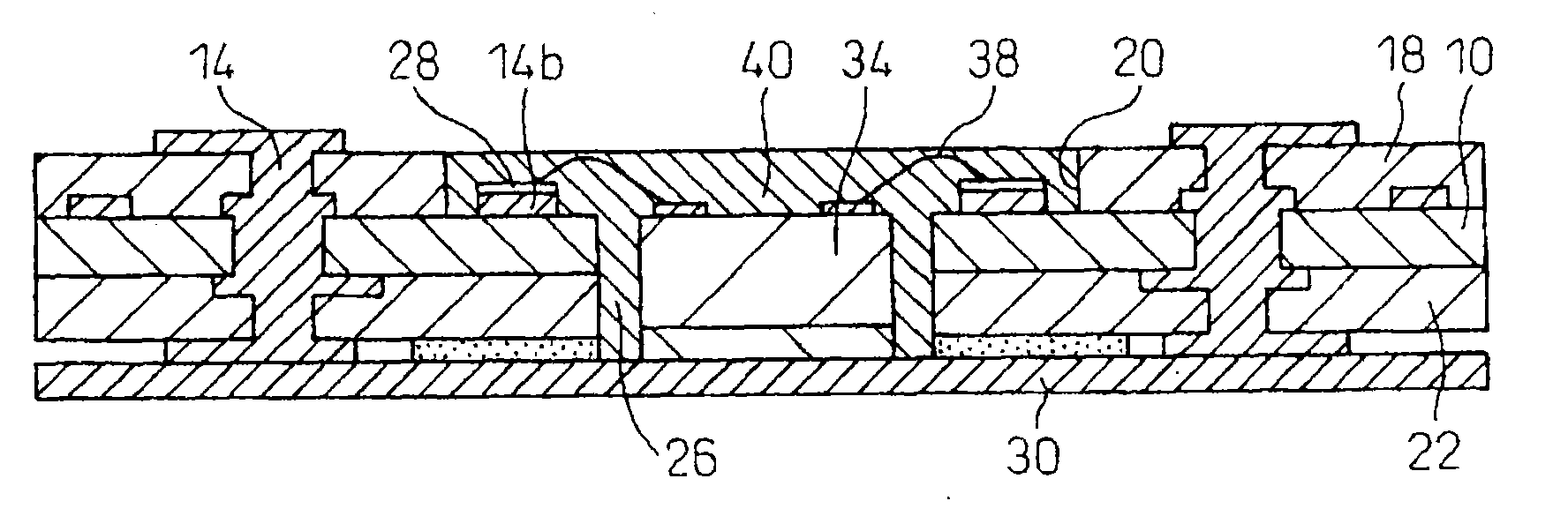
图1显示了形成有配线图案的芯材。准备好由玻璃环氧材料或类似物形成的通常用作配线基板的材料的板状芯材10,并通过熟知的适当的方法在芯材10中形成通孔12。将包括有通孔12的芯材10镀铜或类似物。通过减成法对镀铜层进行图案化,由此可形成需要的配线图案14,该配线图案包括有贯穿通孔12的导体过孔14a。还同时将多个连接焊盘14b形成为配线图案14的一部分,并作为在随后的处理中通过引线结合与待安装的电子元件连接的连接导体部分。Fig. 1 shows a core material on which a wiring pattern is formed. A plate-shaped
作为另一种选择,也可使用通过预先在芯材10的每一面上形成铜层而形成的双面覆铜板。在形成通孔后,可对通孔进行镀覆。同样可通过图案化形成包括导体过孔14a和连接焊盘14b的配线图案14。Alternatively, a double-sided copper-clad laminate formed by forming a copper layer on each side of the
图2显示了芯材受到平行剪切后的状态。如图所示,通过平行剪切操作在板状芯材10中形成贯穿芯材10的开口16。此开口16可利用例如挖孔机或钻头或冲模在芯材10中形成。在引线结合中使用的多个连接焊盘14b布置在芯材10的上表面上各开口16的周围区域中。Figure 2 shows the state of the core material after it has been subjected to parallel shear. As shown, an
图3显示了在芯材的上下表面上形成树脂层的状态。在芯材10的上表面上设置由预浸料坯形成的绝缘树脂层18。同样地,在芯材10的下表面上形成由预浸料坯形成的绝缘树脂层22。在芯材10的上表面上的绝缘树脂层18中预先形成比芯材10的开口16大的开口20。同样地,在芯材10的下表面上的绝缘树脂层22中预先形成大小和形状与开口16相同的开口24。这些开口20和24也可通过挖孔机或钻头或冲模在预浸树脂中形成。Fig. 3 shows the state where resin layers are formed on the upper and lower surfaces of the core material. An insulating
当绝缘树脂层18和22堆叠在两个表面上时,绝缘树脂层18的开口20和绝缘树脂层22的开口24与芯材10的开口16对准。结果,将要在引线结合中作为连接导体的连接焊盘14b从芯材10的上表面上的绝缘树脂层18的相应开口20中露出。与此同时,芯材10的下表面上的绝缘树脂层22的开口24与芯材10的开口16形状和尺寸彼此相同,因此这些开口相互对准从而产生共有的开口26。When the insulating resin layers 18 and 22 are stacked on both surfaces, the
通过利用激光束的过孔处理在设置于芯材10的两个表面上的绝缘树脂层18和22中形成过孔。根据诸如半加成法等熟知的方法,通过施加阻蚀剂(未示出)、对阻蚀剂进行图案化并且镀铜从而以堆叠的方式形成包括过孔导体的配线图案14。Vias are formed in the insulating resin layers 18 and 22 provided on both surfaces of the
图4显示了镀有镍和金的连接焊盘14b的视图。连接焊盘14b是将要在随后的处理中通过引线结合进行电气连接的区域。优选的是,在每个连接焊盘14b上形成镍-金镀层28,特别是在随后的处理中要使用金引线时更是如此。通过施加阻蚀剂(未示出)并对阻蚀剂进行图案化来形成镍-金镀层28,并对位于各连接焊盘14b上方的阻蚀剂图案中的开口镀镍及镀金。FIG. 4 shows a view of the
图5显示了将铜箔结合到基板的绝缘树脂层22上的处理状态。首先,准备好适当宽度和厚度的铜箔30,并将作为结合材料的绝缘抗蚀油墨32印制在铜箔30的结合面一侧。此铜箔30压接结合到基板的下侧,也就是说,结合到绝缘树脂层22的与结合到芯材10上的表面相对的表面上。在安装诸如硅器件或集成电路等电子元件34的后续处理中,此铜箔30将用作支撑部件。FIG. 5 shows the state of the process of bonding the copper foil to the insulating
图6为显示安装电子元件34并实施引线结合后的状态的视图。将电子元件34容纳在由芯材10的开口16和绝缘树脂层22的开口24形成的共有的开口26中,并将电子元件34安装在通过开口26露出的铜箔30上。当安装电子元件34时,预先将作为粘合材料的模片固定薄膜36固定到每个电子元件34的未形成电路的表面上,也就是每个电子元件34的下表面上,并将电子元件34固定到铜箔30上。作为另一种选择,也可通过例如包括硅的倒装法等表面贴装法将电子元件34固定到铜箔30上,而不使用诸如模片固定薄膜36等粘合材料。FIG. 6 is a view showing a state after the
接下来,将形成于每个电子元件34的表面上的多个电极端子34a与覆盖有镍-金镀层28的多个连接焊盘14b通过结合引线38电气连接。由于结合引线38呈环形,必须以这样的方式进行调整:即,将该环的最高位置降低到绝缘树脂层18的开口20的范围内,也就是说,该环不从绝缘树脂层18的上表面向上凸出。换言之,位于芯材10上侧的由预浸料坯形成的绝缘树脂层18必须具有容纳结合引线38的环所需的厚度。金(Au)、铜(Cu)或铝(Al)适于用作结合引线38。Next, the plurality of
图7显示了电子元件34由树脂密封的状态。采用密封树脂40填充由芯材10的开口16和绝缘树脂层22的开口24构成的每一个所共有的开口26以及包括位于开口26之上的引线结合区域在内的绝缘树脂层18的开口20。结果,以绝缘的方式密封电子元件34和结合引线38。可将成型树脂、填充树脂、底部填充树脂等用作密封树脂40。FIG. 7 shows a state where the
图8显示了去除作为支撑层的铜箔并在基板的两个表面上设置绝缘树脂层的状态。利用例如可溶解铜的适当蚀刻剂将作为支撑层的铜箔30剥落并去除。在基板的两个表面通过灰化而变粗糙之后,在基板的两个表面上形成由与绝缘树脂层18和22的材料相似的材料(也就是预浸料坯)形成的绝缘树脂层42和44。因此,由于去除了铜箔30,使基板的两个表面覆盖有同质材料的绝缘树脂,从而可减少由于热膨胀系数差异而造成的基板翘曲。FIG. 8 shows a state where copper foil as a support layer is removed and insulating resin layers are provided on both surfaces of the substrate. The
图9显示了在基板的两个表面上的绝缘树脂层中形成配线的状态。通过利用激光束的过孔处理在形成于基板的两个表面上的绝缘树脂层42和44中形成过孔。通过施加阻蚀剂(未示出)、对阻蚀剂进行图案化并镀铜,以堆叠的方式形成包括有过孔导体部分的配线图案14。FIG. 9 shows a state where wiring is formed in insulating resin layers on both surfaces of the substrate. Vias are formed in the insulating resin layers 42 and 44 formed on both surfaces of the substrate by via processing using a laser beam. The
图10为显示对阻蚀剂进行图案化的状态的视图。将阻蚀剂46施加到基板的一个表面上的形成有配线图案14的绝缘树脂层42上,并将阻蚀剂48施加基板的另一个表面上的形成有配线图案14的绝缘树脂层44上。对这些阻蚀剂进行图案化。配线图案通过阻蚀剂46和48的图案化开口露出的部分构成了例如在后续处理中用于安装表面安装元件的连接焊盘46a。作为另一种选择,将露出的部分作为用于与诸如焊料凸点等外部连接端子连接的连接焊盘48a。FIG. 10 is a view showing a state where a resist is patterned. A resist 46 is applied to the insulating
图11显示了进行切割的状态。所示出的区域与基板中至少包括一个电子元件34的区域相对应。通过沿着平面L进行切割将该基板切分成构成单独的半导体器件的单元。Figure 11 shows the state in which cutting is performed. The regions shown correspond to regions of the substrate comprising at least one
图12显示了安装表面安装元件并形成外部连接端子的状态。在被切分成一个半导体器件单元的安装有电子元件的多层配线基板中,通过表面安装技术(SMT)经由连接焊盘46a安装表面安装元件50,或者在用于连接外部连接端子的连接焊盘48a上形成焊料凸点52。Fig. 12 shows a state where surface mount components are mounted and external connection terminals are formed. In the multilayer wiring board on which electronic components are mounted cut into one semiconductor device unit,
在本发明第一实施例的安装有电子元件的多层配线基板中,在使用平行剪切的芯材10(也就是具有开口16的芯材)或者使用由预浸料坯形成的具有开口24的绝缘树脂层22的结构中,即使基板的电子元件34和连接焊盘14b利用引线结合而电气连接在一起,也可将诸如集成电路等的电子元件34容纳在为芯材10和绝缘树脂层22所共有的各开口26中,并可将结合引线38容纳在绝缘树脂层18的各开口20中。因此,与在现有技术的安装有电子元件的多层配线基板中将电子元件安装在基板的上表面上并通过引线结合进行连接的情况相比,可显著地减少安装有电子元件34的多层配线基板的厚度。In the multilayer wiring board mounted with electronic components according to the first embodiment of the present invention, when using the parallel cut core material 10 (that is, the core material having the opening 16) or using a prepreg having the opening In the structure of the insulating
由于以平行剪切的方式堆叠芯材10和绝缘树脂层22,则可通过利用电子元件34和引线结合部分的平行剪切的开口20和26进行密封树脂40的填充。在填充密封树脂40时开口20和26充当框架,由此可通过拦阻的作用防止熔化的树脂溢流。Since the
图13至17依次显示了用于制造本发明第二实施例的安装有电子元件的多层配线基板的方法。由于第二实施例与第一实施例从准备图1至7中所示的芯材10并形成配线图案的处理(图1)到填充密封树脂的处理(图7)均相同,因此省略其重复的说明。13 to 17 sequentially show a method for manufacturing an electronic component mounted multilayer wiring board according to a second embodiment of the present invention. Since the second embodiment is the same as the first embodiment from the process of preparing the
图13显示了剥落并去除铜箔30然后在芯材的两个表面上形成绝缘树脂层的状态。将电子元件34安装在基板上(图6),并且采用密封树脂40填充开口26和20,从而以绝缘的方式密封住电子元件34和结合引线38(图7)。在第二实施例中,随后在图13中利用可溶解例如铜等的蚀刻剂溶解并去除在安装电子元件34时充当支撑层的铜箔30。然而,铜箔30被溶解的范围部分地受到限制,并且仅在与安装电子元件34的下表面相对应的区域存留有铜箔30的一部分。具体而言,当利用蚀刻剂溶解铜箔30并将其从背面去除时,在进行蚀刻的过程中途暂时中止处理,并且只在下表面上与电子元件34相对应的区域覆盖适当的掩模,由此仅继续对其它的区域进行蚀刻。因此,完全去除铜箔而只在下表面上与电子元件34相对应的区域部分地存留有铜箔30a。为了使电子元件的散热特性更为适当,当将电子元件34安装在作为支撑层的铜箔30上时,也可在电子元件34与铜箔30之间插入散热板。FIG. 13 shows a state where the
如同第一实施例的情况,在基板的两个表面上的树脂通过灰化而变粗糙之后,在基板的两个表面上形成由与绝缘树脂层18和22的材料相似的材料形成的绝缘树脂层42和44。如上所述,铜箔30的大部分被去除,并且在基板的两个表面上都覆盖有由同质材料形成的绝缘树脂层42和44,由此可减少由于热膨胀系数差异而引起的基板发生翘曲的几率。As in the case of the first embodiment, after the resin on both surfaces of the substrate is roughened by ashing, an insulating resin formed of a material similar to that of the insulating resin layers 18 and 22 is formed on both surfaces of the substrate Layers 42 and 44. As described above, most of the
图14显示了在设置于基板的两个表面上的绝缘树脂层中形成配线的状态。如同第一实施例的情况,通过利用激光束或类似物的过孔处理在形成于基板的两个表面上的绝缘树脂层42和44中形成过孔。然而,在过孔处理的同时,在绝缘树脂层44的覆盖着存留于电子元件34下表面上的铜箔30a的区域中形成孔或槽44a,由此部分地露出铜箔30a。因此,剩余的铜箔30a可充当电子元件34的散热部分。FIG. 14 shows a state where wiring is formed in insulating resin layers provided on both surfaces of the substrate. As in the case of the first embodiment, via holes are formed in the insulating resin layers 42 and 44 formed on both surfaces of the substrate by via processing using a laser beam or the like. However, at the same time as the via processing, a hole or
如同第一实施例的情况,在过孔处理之后,可形成包括过孔导体部分的配线图案14,以便于通过施加阻蚀剂(未示出)、对阻蚀剂进行图案化以及镀铜而进一步进行堆叠。As in the case of the first embodiment, after the via processing, the
图15为显示对阻蚀剂进行图案化的状态的视图。如同第一实施例的情况,将阻蚀剂46和48分别施加到基板的两个表面上的形成有配线图案的相应绝缘树脂层42和44上,并对这些阻蚀剂进行图案化。在这种情况下,可将阻蚀剂48中与电子元件34下表面上的铜箔30a相对应的区域作为开口48b,以便于通过铜箔30a使电子元件34具有良好的散热特性。配线图案通过阻蚀剂46的其它图案开口露出的部分形成为例如在后续处理中用于安装表面安装元件的连接焊盘46a。作为另一种选择,可将配线图案通过阻蚀剂48的其它图案开口露出的部分用作例如用于与焊料凸点等外部连接端子连接的连接焊盘48a。FIG. 15 is a view showing a state in which a resist is patterned. As in the case of the first embodiment, resists 46 and 48 are respectively applied to the respective insulating resin layers 42 and 44 formed with wiring patterns on both surfaces of the substrate, and these resists are patterned. In this case, the area of the corrosion resist 48 corresponding to the
图16显示了进行切割的状态。如同第一实施例的情况,所示出的区域与基板中至少包括一个电子元件34的区域相对应。通过沿着平面L进行切割将该基板切分成构成单独的半导体器件的单元。Fig. 16 shows the state in which cutting is performed. As in the case of the first embodiment, the shown area corresponds to the area of the substrate comprising at least one
图17显示了安装表面安装元件并形成外部连接端子的状态。如同第一实施例的情况,在被切分成一个半导体器件单元的安装有电子元件的多层配线基板中,通过表面安装技术(SMT)经由连接焊盘46a安装表面安装元件50,或者在用于连接外部连接端子的连接焊盘48a上形成焊料凸点52。Fig. 17 shows a state where surface mount components are mounted and external connection terminals are formed. As in the case of the first embodiment, in the electronic component-mounted multilayer wiring board cut into one semiconductor device unit, the
如同第一实施例的情况,在本发明第二实施例的安装有电子元件的多层配线基板中,在使用平行剪切的芯材10(也就是具有开口16的芯材)或者使用由预浸料坯形成的具有开口24的绝缘树脂层22的结构中,即使基板的电子元件34和连接焊盘14b利用引线结合而电气连接在一起,也可将诸如集成电路等的电子元件34容纳在为芯材10和绝缘树脂层22所共有的各开口26中,并可将结合引线38容纳在绝缘树脂层18的各开口20中。因此,与在现有技术的安装有电子元件的多层配线基板中将电子元件安装在基板的上表面上并通过引线结合进行连接的情况相比,可显著地减少安装有电子元件34的多层配线基板的厚度。As in the case of the first embodiment, in the electronic component mounted multilayer wiring board of the second embodiment of the present invention, in the case of using the parallel cut core material 10 (that is, the core material having the opening 16) or using the In the structure of the insulating
在采用本发明第二实施例的制造方法所制造的安装有电子元件的多层配线基板中,表现出高导热性的铜箔30部分地存留在各电子元件34的下表面上。在绝缘树脂层44中与铜箔30的该区域相对应的区域中形成孔或槽44a,由此可部分地露出铜箔30。结果,铜箔30可充当电子元件34的散热部分,从而可以获得表现出良好散热特性的安装有电子元件的多层配线基板。In the electronic component mounted multilayer wiring board manufactured by the manufacturing method of the second embodiment of the present invention, the
图18至23依照处理的次序显示了用于制造本发明第三实施例的安装有电子元件的多层配线基板的方法。由于第三实施例与第一实施例从准备图1至5中所示的芯材10并形成配线图案的处理(图1)到将作为支撑层的铜箔压接到基板上的处理(图5)均相同,因此省略其重复的说明。18 to 23 show a method for manufacturing an electronic component mounted multilayer wiring substrate according to a third embodiment of the present invention in the order of processing. Since the third embodiment differs from the first embodiment from the process of preparing the
图18为显示将两个堆叠的电子元件(半导体芯片)60和62安装在基板上并且上部电子元件60进行引线结合后的状态的视图。如同在前述实施例中所使用的电子元件的情况,电极端子60a设置在两个电子元件60和62中的上部电子元件60的上表面上,并且电极端子60a通过引线结合连接。与前述实施例中所使用的电子元件相比,该电子元件必须具有更小的厚度。FIG. 18 is a view showing a state after two stacked electronic components (semiconductor chips) 60 and 62 are mounted on a substrate and the upper
另一个设置在下部位置的电子元件62为表面安装型,并且在电子元件62的下表面上设置有由凸点形成的连接端子62a。这种堆叠型的电子元件60和62在堆叠状态下其厚度必须降低到在芯材10和绝缘树脂层22中形成的共有的开口26的深度之内。可将多种器件作为这种堆叠型的两个电子元件60和62。然而,需将器件预先固定在一起,然后安装在基板上。Another
通过将作为粘合剂的模片固定薄膜36结合到电子元件62的下表面,然后通过加热和加压将电子元件62结合到铜箔30上,从而将下部电子元件62的下表面与铜箔30压接在一起。电子元件62的连接端子62a与铜箔30通过压焊而电气连接在一起。The lower surface of the lower
在上部电子元件60的表面上形成的多个电极端子60a与覆盖有镍-金镀层28的多个连接焊盘14b通过结合引线38电气连接在一起。由于结合引线38呈环形,必须以这样的方式进行调整:即,将该环的最高位置降低到绝缘树脂层18的开口20的范围内,也就是说,该环不从绝缘树脂层18的上表面向上凸出。换言之,由预浸料坯形成的绝缘树脂层18必须具有容纳结合引线38的环所需的厚度。金(Au)、铜(Cu)或铝(Al)适于用作结合引线38。The plurality of
当将堆叠型的电子元件(半导体芯片)60和62安装在铜箔30上时,也可以如前所述在将两个电子元件60和62结合在一起之后通过一项操作来安装这两个电子元件。作为另一种选择,也可首先安装下部电子元件62,并将连接端子62a连接到铜箔上。随后,将上部电子元件60安装在下部电子元件62上,然后将上部电子元件60进行引线结合。When the stacked type electronic components (semiconductor chips) 60 and 62 are mounted on the
图19显示了电子元件由树脂密封的状态。采用密封树脂40填充共有的开口26以及包括位于开口26之上的引线结合区域在内的绝缘树脂层18的开口20。结果,以绝缘的方式密封电子元件60、62和结合引线38。可将成型树脂、填充树脂、底部填充树脂等用作密封树脂40。Fig. 19 shows the state where the electronic components are sealed with resin. The
图20显示了去除作为支撑层的铜箔并在基板的两个表面上设置绝缘树脂层的状态。利用例如可溶解铜的适当蚀刻剂将在安装两个电子元件60和62时作为支撑层的铜箔30剥落并去除。然而,铜箔30被溶解的范围部分地受到限制,由此可形成连接到下部电子元件62的连接端子62a上的配线图案64。具体而言,当利用蚀刻剂溶解铜箔30并将其从背面去除时,在进行蚀刻的过程中途暂时中止处理,并且只在下表面上与连接到电子元件62的连接端子62a上的配线图案64相对应的区域覆盖有适当的掩模,由此仅继续对其它的区域进行蚀刻。因此,完全去除铜箔而只留下配线图案64。FIG. 20 shows a state where copper foil as a support layer is removed and insulating resin layers are provided on both surfaces of the substrate. The
如同前述实施例的情况,在基板的两个表面上的树脂通过灰化而变粗糙之后,在基板的两个表面上形成由与绝缘树脂层18和22的材料相似的材料形成的绝缘树脂层42和44。如上所述,铜箔30的大部分被去除,并且在基板的两个表面上都覆盖有由同质材料形成的绝缘树脂层,由此可减少由于热膨胀系数差异而引起的基板发生翘曲的几率。As in the case of the foregoing embodiments, after the resin on both surfaces of the substrate is roughened by ashing, insulating resin layers formed of a material similar to those of the insulating resin layers 18 and 22 are formed on both surfaces of the
图21显示了在设置于基板的两个表面上的绝缘树脂层中形成配线的状态。如同前述实施例的情况,通过利用激光束或类似物的过孔处理在形成于基板的两个表面上的绝缘树脂层42和44中形成过孔。然而,在过孔处理过程中,也可同时形成用于产生连接到配线图案64上的导体过孔的过孔,其中配线图案64连接到电子元件62的连接端子62a上。FIG. 21 shows a state where wiring is formed in insulating resin layers provided on both surfaces of the substrate. As in the case of the foregoing embodiments, via holes are formed in the insulating resin layers 42 and 44 formed on both surfaces of the substrate by via processing using a laser beam or the like. However, during the via processing, via holes for creating conductor via holes connected to the
如同前述实施例的情况,在过孔处理之后,可形成包括过孔导体部分的配线图案14,以便于通过施加阻蚀剂(未示出)、对阻蚀剂进行图案化以及镀铜而进一步进行堆叠。As in the case of the foregoing embodiments, after the via processing, the
图22为显示对阻蚀剂进行图案化的状态的视图。如同前述实施例的情况,将阻蚀剂46和48施加到基板的两个表面上的形成有配线图案的相应绝缘树脂层42和44上。对这些阻蚀剂进行图案化。配线图案通过阻蚀剂46的其它图案开口露出的部分形成为例如在后续处理中用于安装表面安装元件的连接焊盘46a。作为另一种选择,可将配线图案通过阻蚀剂48的其它图案开口露出的部分用作例如用于与焊料凸点等外部连接端子连接的连接焊盘48a。FIG. 22 is a view showing a state in which a resist is patterned. As in the case of the foregoing embodiments, resists 46 and 48 are applied to the respective insulating resin layers 42 and 44 formed with wiring patterns on both surfaces of the substrate. These resists are patterned. Portions of the wiring pattern exposed through other pattern openings of the resist 46 are formed, for example, as
图23显示了进行切割的状态。所示出的区域与基板中至少包括一个电子元件34的区域相对应。通过沿着平面L进行切割将该基板切分成构成单独的半导体器件的单元。Fig. 23 shows the state in which cutting is performed. The regions shown correspond to regions of the substrate comprising at least one
图24显示了安装表面安装元件并形成外部连接端子的状态。如同前述实施例的情况,在被切分成一个半导体器件单元的第三实施例的安装有电子元件的多层配线基板中,通过表面安装技术(SMT)经由连接焊盘46a安装表面安装元件50,或者在用于连接外部连接端子的连接焊盘48a上形成焊料凸点52。Fig. 24 shows a state where surface mount components are mounted and external connection terminals are formed. As in the case of the foregoing embodiments, in the electronic component-mounted multilayer wiring board of the third embodiment cut into one semiconductor device unit,
除了产生与第一和第二实施例相同的效果之外,本发明第三实施例的安装有电子元件的多层配线基板还使得能够在多层配线基板上安装连接类型彼此不同的引线结合型电子元件与表面安装电子元件构成的堆叠型电子元件。In addition to producing the same effects as those of the first and second embodiments, the electronic component mounted multilayer wiring board of the third embodiment of the present invention enables mounting of leads whose connection types are different from each other on the multilayer wiring board Stacked electronic components composed of combined electronic components and surface mount electronic components.
尽管参照附图对本发明的各实施例进行了说明,但本发明并不局限于这些实施例,并且可表现为多种形式或者在本发明的实质及范围内可具有多种变更或变型。Although the embodiments of the present invention have been described with reference to the drawings, the present invention is not limited to these embodiments, and can be embodied in various forms or have various changes or modifications within the spirit and scope of the present invention.
如上所述,根据本发明,诸如集成电路等的电子元件容纳在芯材层的开口中,并且利用预浸树脂层的开口通过引线结合将电子元件与连接导体部分电气连接在一起。与在现有技术的安装有电子元件的多层配线基板中将电子元件直接安装在基板的上表面上并通过引线结合进行连接的情况相比,可显著地减少安装有电子元件的多层配线基板的厚度。这样,可以得到安装有电子元件的薄多层配线基板。As described above, according to the present invention, an electronic component such as an integrated circuit is housed in the opening of the core material layer, and the electronic component and the connection conductor portion are electrically connected together by wire bonding using the opening of the prepreg layer. Compared with the case where the electronic components are directly mounted on the upper surface of the substrate and connected by wire bonding in the prior art multilayer wiring substrate mounted with electronic components, the number of multilayer wiring boards mounted with electronic components can be significantly reduced. The thickness of the wiring board. In this way, a thin multilayer wiring board mounted with electronic components can be obtained.
由于对芯材和预浸树脂层进行平行剪切式堆叠,因此可利用电子元件与引线结合部分的平行剪切开口填充密封树脂,由此可防止密封树脂溢流。也就是说,可以表现出拦阻的效果。Since the core material and the prepreg layers are stacked in parallel shear, the sealing resin can be filled using the parallel shear openings where the electronic components are bonded to the leads, thereby preventing the sealing resin from overflowing. That is to say, a blocking effect can be manifested.
本申请要求2006年10月20日在日本专利局提交的日本专利申请No.2006-286300的优先权,该日本专利申请的全部内容以引用的方式并入本文。This application claims priority from Japanese Patent Application No. 2006-286300 filed in the Japan Patent Office on October 20, 2006, the entire contents of which are incorporated herein by reference.
Claims (17)
Applications Claiming Priority (2)
| Application Number | Priority Date | Filing Date | Title |
|---|---|---|---|
| JP2006286300A JP5100081B2 (en) | 2006-10-20 | 2006-10-20 | Electronic component-mounted multilayer wiring board and manufacturing method thereof |
| JP2006286300 | 2006-10-20 |
Publications (1)
| Publication Number | Publication Date |
|---|---|
| CN101166394A true CN101166394A (en) | 2008-04-23 |
Family
ID=38963125
Family Applications (1)
| Application Number | Title | Priority Date | Filing Date |
|---|---|---|---|
| CNA2007101632526A Pending CN101166394A (en) | 2006-10-20 | 2007-10-19 | Multilayer wiring board mounted with electronic components and manufacturing method thereof |
Country Status (6)
| Country | Link |
|---|---|
| US (2) | US7923367B2 (en) |
| EP (1) | EP1915038A1 (en) |
| JP (1) | JP5100081B2 (en) |
| KR (1) | KR20080035974A (en) |
| CN (1) | CN101166394A (en) |
| TW (1) | TW200822833A (en) |
Cited By (13)
| Publication number | Priority date | Publication date | Assignee | Title |
|---|---|---|---|---|
| CN102065638A (en) * | 2009-11-17 | 2011-05-18 | 三星电机株式会社 | Printed circuit board having electro-component and manufacturing method thereof |
| CN102256452A (en) * | 2010-04-02 | 2011-11-23 | 株式会社电装 | Circuit board with built-in semiconductor chip and method of manufacturing the same |
| CN102820272A (en) * | 2011-06-07 | 2012-12-12 | 欣兴电子股份有限公司 | Package structure embedded with electronic components and its manufacturing method |
| CN103052281A (en) * | 2011-10-14 | 2013-04-17 | 富葵精密组件(深圳)有限公司 | Embedded multilayer circuit board and manufacturing method thereof |
| CN101930956B (en) * | 2009-06-22 | 2013-09-25 | 日月光半导体制造股份有限公司 | Chip packaging structure and manufacturing method thereof |
| CN106352136A (en) * | 2015-07-15 | 2017-01-25 | 阿自倍尔株式会社 | Positioner |
| CN106352137A (en) * | 2015-07-15 | 2017-01-25 | 阿自倍尔株式会社 | Positioner |
| CN107039290A (en) * | 2015-12-31 | 2017-08-11 | 台湾积体电路制造股份有限公司 | Semiconductor devices and its manufacture method |
| CN111009500A (en) * | 2018-10-05 | 2020-04-14 | 三星电子株式会社 | Semiconductor package, method of manufacturing the same, and method of manufacturing redistribution structure |
| CN111465247A (en) * | 2020-04-10 | 2020-07-28 | 河南工业职业技术学院 | PCB substrate mounting structure and electronic component system |
| CN111952273A (en) * | 2016-10-25 | 2020-11-17 | 日月光半导体制造股份有限公司 | Semiconductor device package and method of manufacturing the same |
| CN113327898A (en) * | 2020-02-28 | 2021-08-31 | 深南电路股份有限公司 | Manufacturing method of packaging structure and packaging structure |
| US12622096B2 (en) | 2022-07-29 | 2026-05-05 | HKC Corporation Limited | Display panel and preparation method thereof |
Families Citing this family (39)
| Publication number | Priority date | Publication date | Assignee | Title |
|---|---|---|---|---|
| JP4073945B1 (en) * | 2007-01-12 | 2008-04-09 | 新光電気工業株式会社 | Manufacturing method of multilayer wiring board |
| US20090127686A1 (en) * | 2007-11-21 | 2009-05-21 | Advanced Chip Engineering Technology Inc. | Stacking die package structure for semiconductor devices and method of the same |
| EP2161747A1 (en) * | 2008-09-04 | 2010-03-10 | Shinko Electric Industries Co., Ltd. | Electronic component package and method of manufacturing the same |
| US7858441B2 (en) * | 2008-12-08 | 2010-12-28 | Stats Chippac, Ltd. | Semiconductor package with semiconductor core structure and method of forming same |
| KR101055509B1 (en) * | 2009-03-19 | 2011-08-08 | 삼성전기주식회사 | Electronic component embedded printed circuit board |
| JP5641701B2 (en) * | 2009-03-25 | 2014-12-17 | 株式会社東芝 | 3D semiconductor integrated circuit |
| US7868449B2 (en) * | 2009-05-25 | 2011-01-11 | Freescale Semiconductor, Inc. | Semiconductor substrate and method of connecting semiconductor die to substrate |
| TW201110285A (en) | 2009-09-08 | 2011-03-16 | Unimicron Technology Corp | Package structure having embedded semiconductor element and method of forming the same |
| US8461462B2 (en) * | 2009-09-28 | 2013-06-11 | Kyocera Corporation | Circuit substrate, laminated board and laminated sheet |
| US20120314390A1 (en) * | 2010-03-03 | 2012-12-13 | Mutual-Tek Industries Co., Ltd. | Multilayer circuit board |
| JP2011216634A (en) * | 2010-03-31 | 2011-10-27 | Murata Mfg Co Ltd | Substrate with built-in electronic component, electronic circuit module, and method for manufacturing of substrate with built-in electronic component |
| TWI399149B (en) * | 2010-07-09 | 2013-06-11 | Unimicron Technology Corp | Wiring board and method for fabricating the same |
| WO2012015085A1 (en) * | 2010-07-30 | 2012-02-02 | Lg Innotek Co., Ltd. | Printed circuit board and method of manufacturing the same |
| TWI420996B (en) * | 2010-07-30 | 2013-12-21 | Lg伊諾特股份有限公司 | Printed circuit board and method of manufacturing same |
| CN103052501B (en) * | 2010-07-30 | 2015-08-26 | 京瓷株式会社 | Insulating trip, its manufacture method and have employed the manufacture method of structure of this insulating trip |
| JP5672305B2 (en) * | 2010-08-27 | 2015-02-18 | 株式会社村田製作所 | Semiconductor device |
| US9944554B2 (en) * | 2011-09-15 | 2018-04-17 | Apple Inc. | Perforated mother sheet for partial edge chemical strengthening and method therefor |
| DE102011088256A1 (en) * | 2011-12-12 | 2013-06-13 | Zf Friedrichshafen Ag | Multilayer printed circuit board and arrangement with such |
| US9236322B2 (en) * | 2012-04-11 | 2016-01-12 | Taiwan Semiconductor Manufacturing Company, Ltd. | Methods and apparatus for heat spreader on silicon |
| JP5539453B2 (en) * | 2012-07-17 | 2014-07-02 | 新光電気工業株式会社 | Electronic component-mounted multilayer wiring board and manufacturing method thereof |
| JP5590097B2 (en) * | 2012-10-29 | 2014-09-17 | 大日本印刷株式会社 | Component built-in wiring board |
| CN103904061A (en) * | 2012-12-25 | 2014-07-02 | 欣兴电子股份有限公司 | Embedded electronic component packaging structure |
| US8803310B1 (en) * | 2013-02-08 | 2014-08-12 | Unimicron Technology Corp. | Embedded electronic device package structure |
| KR20140134479A (en) * | 2013-05-14 | 2014-11-24 | 삼성전기주식회사 | Printed circuit board |
| JP2015130443A (en) * | 2014-01-08 | 2015-07-16 | 富士通株式会社 | Method of manufacturing component built-in substrate |
| KR102186149B1 (en) * | 2015-03-11 | 2020-12-03 | 삼성전기주식회사 | Printed circuit board and method for manufacturing the same |
| KR102253472B1 (en) * | 2015-03-13 | 2021-05-18 | 삼성전기주식회사 | Printed Circuit Board and Method of the Same |
| US10109588B2 (en) * | 2015-05-15 | 2018-10-23 | Samsung Electro-Mechanics Co., Ltd. | Electronic component package and package-on-package structure including the same |
| KR102662856B1 (en) * | 2016-03-31 | 2024-05-07 | 삼성전기주식회사 | Printed circuit board and camera module having the same |
| CN107295747B (en) * | 2016-03-31 | 2021-03-12 | 奥特斯(中国)有限公司 | Device carrier and method of making device carrier |
| JP2019067858A (en) * | 2017-09-29 | 2019-04-25 | イビデン株式会社 | Printed wiring board and manufacturing method thereof |
| JP2019067994A (en) * | 2017-10-04 | 2019-04-25 | トヨタ自動車株式会社 | Multilayer substrate and manufacturing method thereof |
| JP2019178054A (en) * | 2018-03-30 | 2019-10-17 | Tdk株式会社 | Core material and heat dissipation substrate |
| US20200006210A1 (en) * | 2018-06-27 | 2020-01-02 | Intel Corporation | Chip package and method of manufacturing |
| JP7080322B2 (en) * | 2018-07-12 | 2022-06-03 | 三菱電機株式会社 | Semiconductor device |
| DE102018126388A1 (en) * | 2018-10-23 | 2020-04-23 | Bluenetics GmbH | Control switch module for flush-mounted or surface-mounted boxes and method for producing a printed circuit board for such a control switch module |
| CN111199922A (en) * | 2018-11-20 | 2020-05-26 | 奥特斯科技(重庆)有限公司 | Component carrier and method of making the same |
| WO2022000191A1 (en) * | 2020-06-29 | 2022-01-06 | 庆鼎精密电子(淮安)有限公司 | Embedded circuit board and manufacturing method therefor |
| CN113808954B (en) * | 2021-08-10 | 2026-04-14 | 珠海越亚半导体股份有限公司 | Mixed embedded packaging structure and manufacturing method thereof |
Family Cites Families (14)
| Publication number | Priority date | Publication date | Assignee | Title |
|---|---|---|---|---|
| US5237204A (en) | 1984-05-25 | 1993-08-17 | Compagnie D'informatique Militaire Spatiale Et Aeronautique | Electric potential distribution device and an electronic component case incorporating such a device |
| JP3235452B2 (en) | 1995-03-20 | 2001-12-04 | 松下電器産業株式会社 | High frequency integrated circuit device |
| JP3928753B2 (en) * | 1996-08-06 | 2007-06-13 | 日立化成工業株式会社 | Multi-chip mounting method and manufacturing method of chip with adhesive |
| JPH11126978A (en) | 1997-10-24 | 1999-05-11 | Kyocera Corp | Multilayer wiring board |
| SE514426C2 (en) | 1999-06-17 | 2001-02-19 | Ericsson Telefon Ab L M | Device for chip mounting in cavity in multilayer PCBs |
| JP2001313474A (en) | 2000-02-21 | 2001-11-09 | Ngk Spark Plug Co Ltd | Wiring board |
| JP2002158312A (en) * | 2000-11-17 | 2002-05-31 | Oki Electric Ind Co Ltd | Semiconductor package for three-dimensional mounting, manufacturing method thereof, and semiconductor device |
| JP3890947B2 (en) | 2001-10-17 | 2007-03-07 | 松下電器産業株式会社 | High frequency semiconductor device |
| JP2003224228A (en) * | 2002-01-31 | 2003-08-08 | Shinko Electric Ind Co Ltd | Package for semiconductor device, semiconductor device and method of manufacturing the same |
| JP2003282771A (en) * | 2002-03-20 | 2003-10-03 | Kyocera Corp | Wiring board with heat sink |
| JP4167001B2 (en) * | 2002-04-15 | 2008-10-15 | 日本特殊陶業株式会社 | Wiring board manufacturing method |
| JP2004047528A (en) | 2002-07-09 | 2004-02-12 | Nec Electronics Corp | Semiconductor substrate and method of manufacturing the same |
| JP3709882B2 (en) * | 2003-07-22 | 2005-10-26 | 松下電器産業株式会社 | Circuit module and manufacturing method thereof |
| JP2006165333A (en) | 2004-12-08 | 2006-06-22 | Sony Corp | Semiconductor device mounting apparatus and semiconductor device mounting method |
-
2006
- 2006-10-20 JP JP2006286300A patent/JP5100081B2/en not_active Expired - Fee Related
-
2007
- 2007-10-18 US US11/907,889 patent/US7923367B2/en not_active Expired - Fee Related
- 2007-10-18 KR KR1020070105020A patent/KR20080035974A/en not_active Withdrawn
- 2007-10-19 EP EP07118861A patent/EP1915038A1/en not_active Withdrawn
- 2007-10-19 TW TW096139131A patent/TW200822833A/en unknown
- 2007-10-19 CN CNA2007101632526A patent/CN101166394A/en active Pending
-
2011
- 2011-02-23 US US13/032,975 patent/US8222747B2/en not_active Expired - Fee Related
Cited By (19)
| Publication number | Priority date | Publication date | Assignee | Title |
|---|---|---|---|---|
| CN101930956B (en) * | 2009-06-22 | 2013-09-25 | 日月光半导体制造股份有限公司 | Chip packaging structure and manufacturing method thereof |
| CN102065638A (en) * | 2009-11-17 | 2011-05-18 | 三星电机株式会社 | Printed circuit board having electro-component and manufacturing method thereof |
| CN102256452A (en) * | 2010-04-02 | 2011-11-23 | 株式会社电装 | Circuit board with built-in semiconductor chip and method of manufacturing the same |
| CN102256452B (en) * | 2010-04-02 | 2014-01-29 | 株式会社电装 | Circuit board with built-in semiconductor chip and method of manufacturing the same |
| CN102820272A (en) * | 2011-06-07 | 2012-12-12 | 欣兴电子股份有限公司 | Package structure embedded with electronic components and its manufacturing method |
| CN103052281A (en) * | 2011-10-14 | 2013-04-17 | 富葵精密组件(深圳)有限公司 | Embedded multilayer circuit board and manufacturing method thereof |
| CN106352136A (en) * | 2015-07-15 | 2017-01-25 | 阿自倍尔株式会社 | Positioner |
| CN106352137A (en) * | 2015-07-15 | 2017-01-25 | 阿自倍尔株式会社 | Positioner |
| CN107039290A (en) * | 2015-12-31 | 2017-08-11 | 台湾积体电路制造股份有限公司 | Semiconductor devices and its manufacture method |
| US10515865B2 (en) | 2015-12-31 | 2019-12-24 | Taiwan Semiconductor Manufacturing Company, Ltd. | Underfill control structures and method |
| US11018069B2 (en) | 2015-12-31 | 2021-05-25 | Taiwan Semiconductor Manufacturing Company, Ltd. | Underfill control structures and method |
| CN107039290B (en) * | 2015-12-31 | 2021-06-22 | 台湾积体电路制造股份有限公司 | Semiconductor device and method for manufacturing the same |
| CN111952273A (en) * | 2016-10-25 | 2020-11-17 | 日月光半导体制造股份有限公司 | Semiconductor device package and method of manufacturing the same |
| CN111952273B (en) * | 2016-10-25 | 2023-09-05 | 日月光半导体制造股份有限公司 | Semiconductor device packaging and manufacturing method thereof |
| CN111009500A (en) * | 2018-10-05 | 2020-04-14 | 三星电子株式会社 | Semiconductor package, method of manufacturing the same, and method of manufacturing redistribution structure |
| CN111009500B (en) * | 2018-10-05 | 2026-03-20 | 三星电子株式会社 | Semiconductor package, manufacturing method thereof, and method for manufacturing redistributed structure |
| CN113327898A (en) * | 2020-02-28 | 2021-08-31 | 深南电路股份有限公司 | Manufacturing method of packaging structure and packaging structure |
| CN111465247A (en) * | 2020-04-10 | 2020-07-28 | 河南工业职业技术学院 | PCB substrate mounting structure and electronic component system |
| US12622096B2 (en) | 2022-07-29 | 2026-05-05 | HKC Corporation Limited | Display panel and preparation method thereof |
Also Published As
| Publication number | Publication date |
|---|---|
| US20080099911A1 (en) | 2008-05-01 |
| EP1915038A1 (en) | 2008-04-23 |
| JP5100081B2 (en) | 2012-12-19 |
| US20110140286A1 (en) | 2011-06-16 |
| JP2008103615A (en) | 2008-05-01 |
| US7923367B2 (en) | 2011-04-12 |
| TW200822833A (en) | 2008-05-16 |
| US8222747B2 (en) | 2012-07-17 |
| KR20080035974A (en) | 2008-04-24 |
Similar Documents
| Publication | Publication Date | Title |
|---|---|---|
| CN101166394A (en) | Multilayer wiring board mounted with electronic components and manufacturing method thereof | |
| CN104428892B (en) | Method and apparatus for substrate core layer | |
| US8181342B2 (en) | Method for manufacturing a coreless packaging substrate | |
| CN100364092C (en) | Semiconductor device and production method thereof | |
| JP3813402B2 (en) | Manufacturing method of semiconductor device | |
| KR100395862B1 (en) | Flip chip type semiconductor device and method for manufacturing the same | |
| CN101609830B (en) | Printed circuit board including electronic component embedded therein and method of manufacturing the same | |
| TWI458052B (en) | Wiring board and method of manufacturing same | |
| JPWO2007126090A1 (en) | CIRCUIT BOARD, ELECTRONIC DEVICE DEVICE, AND CIRCUIT BOARD MANUFACTURING METHOD | |
| US20080116562A1 (en) | Carrier structure for semiconductor chip and method for manufacturing the same | |
| JP2016063130A (en) | Printed wiring board and semiconductor package | |
| WO2007102358A1 (en) | Electronic device package, module and electronic device | |
| JP2017152536A (en) | Printed wiring board and manufacturing method thereof | |
| JP2017050310A (en) | Electronic component device and manufacturing method thereof | |
| KR20150135048A (en) | Printed circuit board, method for manufacturing the same and package on packaage having the thereof | |
| JP5003812B2 (en) | Printed wiring board and printed wiring board manufacturing method | |
| JP2017017215A (en) | Wiring board and manufacturing method thereof | |
| JPWO2007138771A1 (en) | Semiconductor device, electronic component module, and method of manufacturing semiconductor device | |
| KR20150065029A (en) | Printed circuit board, manufacturing method thereof and semiconductor package | |
| JP5539453B2 (en) | Electronic component-mounted multilayer wiring board and manufacturing method thereof | |
| KR100908986B1 (en) | Coreless Package Substrate and Manufacturing Method | |
| TWI381500B (en) | Package substrate embedded with semiconductor wafer and preparation method thereof | |
| CN101958292B (en) | Printed circuit board, encapsulation piece and manufacture methods thereof | |
| JP2623980B2 (en) | Manufacturing method of substrate with lead for semiconductor mounting | |
| JPH0595071A (en) | Substrate for mounting electronic parts and manufacturing method thereof |
Legal Events
| Date | Code | Title | Description |
|---|---|---|---|
| C06 | Publication | ||
| PB01 | Publication | ||
| C10 | Entry into substantive examination | ||
| SE01 | Entry into force of request for substantive examination | ||
| C02 | Deemed withdrawal of patent application after publication (patent law 2001) | ||
| WD01 | Invention patent application deemed withdrawn after publication |
Open date: 20080423 |