CN101110201B - Liquid crystal display device and method of driving the same - Google Patents
Liquid crystal display device and method of driving the same Download PDFInfo
- Publication number
- CN101110201B CN101110201B CN2007101294534A CN200710129453A CN101110201B CN 101110201 B CN101110201 B CN 101110201B CN 2007101294534 A CN2007101294534 A CN 2007101294534A CN 200710129453 A CN200710129453 A CN 200710129453A CN 101110201 B CN101110201 B CN 101110201B
- Authority
- CN
- China
- Prior art keywords
- voltage
- calibration
- liquid crystal
- substrate
- electrode
- Prior art date
- Legal status (The legal status is an assumption and is not a legal conclusion. Google has not performed a legal analysis and makes no representation as to the accuracy of the status listed.)
- Expired - Fee Related
Links
Images


Classifications
-
- G—PHYSICS
- G09—EDUCATION; CRYPTOGRAPHY; DISPLAY; ADVERTISING; SEALS
- G09G—ARRANGEMENTS OR CIRCUITS FOR CONTROL OF INDICATING DEVICES USING STATIC MEANS TO PRESENT VARIABLE INFORMATION
- G09G3/00—Control arrangements or circuits, of interest only in connection with visual indicators other than cathode-ray tubes
- G09G3/20—Control arrangements or circuits, of interest only in connection with visual indicators other than cathode-ray tubes for presentation of an assembly of a number of characters, e.g. a page, by composing the assembly by combination of individual elements arranged in a matrix no fixed position being assigned to or needed to be assigned to the individual characters or partial characters
- G09G3/34—Control arrangements or circuits, of interest only in connection with visual indicators other than cathode-ray tubes for presentation of an assembly of a number of characters, e.g. a page, by composing the assembly by combination of individual elements arranged in a matrix no fixed position being assigned to or needed to be assigned to the individual characters or partial characters by control of light from an independent source
- G09G3/36—Control arrangements or circuits, of interest only in connection with visual indicators other than cathode-ray tubes for presentation of an assembly of a number of characters, e.g. a page, by composing the assembly by combination of individual elements arranged in a matrix no fixed position being assigned to or needed to be assigned to the individual characters or partial characters by control of light from an independent source using liquid crystals
-
- G—PHYSICS
- G02—OPTICS
- G02F—OPTICAL DEVICES OR ARRANGEMENTS FOR THE CONTROL OF LIGHT BY MODIFICATION OF THE OPTICAL PROPERTIES OF THE MEDIA OF THE ELEMENTS INVOLVED THEREIN; NON-LINEAR OPTICS; FREQUENCY-CHANGING OF LIGHT; OPTICAL LOGIC ELEMENTS; OPTICAL ANALOGUE/DIGITAL CONVERTERS
- G02F1/00—Devices or arrangements for the control of the intensity, colour, phase, polarisation or direction of light arriving from an independent light source, e.g. switching, gating or modulating; Non-linear optics
- G02F1/01—Devices or arrangements for the control of the intensity, colour, phase, polarisation or direction of light arriving from an independent light source, e.g. switching, gating or modulating; Non-linear optics for the control of the intensity, phase, polarisation or colour
- G02F1/13—Devices or arrangements for the control of the intensity, colour, phase, polarisation or direction of light arriving from an independent light source, e.g. switching, gating or modulating; Non-linear optics for the control of the intensity, phase, polarisation or colour based on liquid crystals, e.g. single liquid crystal display cells
- G02F1/133—Constructional arrangements; Operation of liquid crystal cells; Circuit arrangements
- G02F1/136—Liquid crystal cells structurally associated with a semi-conducting layer or substrate, e.g. cells forming part of an integrated circuit
- G02F1/1362—Active matrix addressed cells
- G02F1/136213—Storage capacitors associated with the pixel electrode
-
- G—PHYSICS
- G02—OPTICS
- G02F—OPTICAL DEVICES OR ARRANGEMENTS FOR THE CONTROL OF LIGHT BY MODIFICATION OF THE OPTICAL PROPERTIES OF THE MEDIA OF THE ELEMENTS INVOLVED THEREIN; NON-LINEAR OPTICS; FREQUENCY-CHANGING OF LIGHT; OPTICAL LOGIC ELEMENTS; OPTICAL ANALOGUE/DIGITAL CONVERTERS
- G02F1/00—Devices or arrangements for the control of the intensity, colour, phase, polarisation or direction of light arriving from an independent light source, e.g. switching, gating or modulating; Non-linear optics
- G02F1/01—Devices or arrangements for the control of the intensity, colour, phase, polarisation or direction of light arriving from an independent light source, e.g. switching, gating or modulating; Non-linear optics for the control of the intensity, phase, polarisation or colour
- G02F1/13—Devices or arrangements for the control of the intensity, colour, phase, polarisation or direction of light arriving from an independent light source, e.g. switching, gating or modulating; Non-linear optics for the control of the intensity, phase, polarisation or colour based on liquid crystals, e.g. single liquid crystal display cells
- G02F1/133—Constructional arrangements; Operation of liquid crystal cells; Circuit arrangements
-
- G—PHYSICS
- G02—OPTICS
- G02F—OPTICAL DEVICES OR ARRANGEMENTS FOR THE CONTROL OF LIGHT BY MODIFICATION OF THE OPTICAL PROPERTIES OF THE MEDIA OF THE ELEMENTS INVOLVED THEREIN; NON-LINEAR OPTICS; FREQUENCY-CHANGING OF LIGHT; OPTICAL LOGIC ELEMENTS; OPTICAL ANALOGUE/DIGITAL CONVERTERS
- G02F1/00—Devices or arrangements for the control of the intensity, colour, phase, polarisation or direction of light arriving from an independent light source, e.g. switching, gating or modulating; Non-linear optics
- G02F1/01—Devices or arrangements for the control of the intensity, colour, phase, polarisation or direction of light arriving from an independent light source, e.g. switching, gating or modulating; Non-linear optics for the control of the intensity, phase, polarisation or colour
- G02F1/13—Devices or arrangements for the control of the intensity, colour, phase, polarisation or direction of light arriving from an independent light source, e.g. switching, gating or modulating; Non-linear optics for the control of the intensity, phase, polarisation or colour based on liquid crystals, e.g. single liquid crystal display cells
- G02F1/137—Devices or arrangements for the control of the intensity, colour, phase, polarisation or direction of light arriving from an independent light source, e.g. switching, gating or modulating; Non-linear optics for the control of the intensity, phase, polarisation or colour based on liquid crystals, e.g. single liquid crystal display cells characterised by the electro-optical or magneto-optical effect, e.g. field-induced phase transition, orientation effect, guest-host interaction or dynamic scattering
- G02F1/139—Devices or arrangements for the control of the intensity, colour, phase, polarisation or direction of light arriving from an independent light source, e.g. switching, gating or modulating; Non-linear optics for the control of the intensity, phase, polarisation or colour based on liquid crystals, e.g. single liquid crystal display cells characterised by the electro-optical or magneto-optical effect, e.g. field-induced phase transition, orientation effect, guest-host interaction or dynamic scattering based on orientation effects in which the liquid crystal remains transparent
- G02F1/1393—Devices or arrangements for the control of the intensity, colour, phase, polarisation or direction of light arriving from an independent light source, e.g. switching, gating or modulating; Non-linear optics for the control of the intensity, phase, polarisation or colour based on liquid crystals, e.g. single liquid crystal display cells characterised by the electro-optical or magneto-optical effect, e.g. field-induced phase transition, orientation effect, guest-host interaction or dynamic scattering based on orientation effects in which the liquid crystal remains transparent the birefringence of the liquid crystal being electrically controlled, e.g. ECB-, DAP-, HAN-, PI-LC cells
- G02F1/1395—Optically compensated birefringence [OCB]- cells or PI- cells
-
- G—PHYSICS
- G09—EDUCATION; CRYPTOGRAPHY; DISPLAY; ADVERTISING; SEALS
- G09G—ARRANGEMENTS OR CIRCUITS FOR CONTROL OF INDICATING DEVICES USING STATIC MEANS TO PRESENT VARIABLE INFORMATION
- G09G3/00—Control arrangements or circuits, of interest only in connection with visual indicators other than cathode-ray tubes
- G09G3/20—Control arrangements or circuits, of interest only in connection with visual indicators other than cathode-ray tubes for presentation of an assembly of a number of characters, e.g. a page, by composing the assembly by combination of individual elements arranged in a matrix no fixed position being assigned to or needed to be assigned to the individual characters or partial characters
- G09G3/34—Control arrangements or circuits, of interest only in connection with visual indicators other than cathode-ray tubes for presentation of an assembly of a number of characters, e.g. a page, by composing the assembly by combination of individual elements arranged in a matrix no fixed position being assigned to or needed to be assigned to the individual characters or partial characters by control of light from an independent source
- G09G3/36—Control arrangements or circuits, of interest only in connection with visual indicators other than cathode-ray tubes for presentation of an assembly of a number of characters, e.g. a page, by composing the assembly by combination of individual elements arranged in a matrix no fixed position being assigned to or needed to be assigned to the individual characters or partial characters by control of light from an independent source using liquid crystals
- G09G3/3611—Control of matrices with row and column drivers
- G09G3/3648—Control of matrices with row and column drivers using an active matrix
- G09G3/3655—Details of drivers for counter electrodes, e.g. common electrodes for pixel capacitors or supplementary storage capacitors
-
- G—PHYSICS
- G09—EDUCATION; CRYPTOGRAPHY; DISPLAY; ADVERTISING; SEALS
- G09G—ARRANGEMENTS OR CIRCUITS FOR CONTROL OF INDICATING DEVICES USING STATIC MEANS TO PRESENT VARIABLE INFORMATION
- G09G2300/00—Aspects of the constitution of display devices
- G09G2300/04—Structural and physical details of display devices
- G09G2300/0469—Details of the physics of pixel operation
- G09G2300/0478—Details of the physics of pixel operation related to liquid crystal pixels
- G09G2300/0491—Use of a bi-refringent liquid crystal, optically controlled bi-refringence [OCB] with bend and splay states, or electrically controlled bi-refringence [ECB] for controlling the color
-
- G—PHYSICS
- G09—EDUCATION; CRYPTOGRAPHY; DISPLAY; ADVERTISING; SEALS
- G09G—ARRANGEMENTS OR CIRCUITS FOR CONTROL OF INDICATING DEVICES USING STATIC MEANS TO PRESENT VARIABLE INFORMATION
- G09G2310/00—Command of the display device
- G09G2310/02—Addressing, scanning or driving the display screen or processing steps related thereto
- G09G2310/0243—Details of the generation of driving signals
- G09G2310/0245—Clearing or presetting the whole screen independently of waveforms, e.g. on power-on
-
- G—PHYSICS
- G09—EDUCATION; CRYPTOGRAPHY; DISPLAY; ADVERTISING; SEALS
- G09G—ARRANGEMENTS OR CIRCUITS FOR CONTROL OF INDICATING DEVICES USING STATIC MEANS TO PRESENT VARIABLE INFORMATION
- G09G2310/00—Command of the display device
- G09G2310/06—Details of flat display driving waveforms
-
- G—PHYSICS
- G09—EDUCATION; CRYPTOGRAPHY; DISPLAY; ADVERTISING; SEALS
- G09G—ARRANGEMENTS OR CIRCUITS FOR CONTROL OF INDICATING DEVICES USING STATIC MEANS TO PRESENT VARIABLE INFORMATION
- G09G2320/00—Control of display operating conditions
- G09G2320/02—Improving the quality of display appearance
- G09G2320/0247—Flicker reduction other than flicker reduction circuits used for single beam cathode-ray tubes
-
- G—PHYSICS
- G09—EDUCATION; CRYPTOGRAPHY; DISPLAY; ADVERTISING; SEALS
- G09G—ARRANGEMENTS OR CIRCUITS FOR CONTROL OF INDICATING DEVICES USING STATIC MEANS TO PRESENT VARIABLE INFORMATION
- G09G2330/00—Aspects of power supply; Aspects of display protection and defect management
- G09G2330/02—Details of power systems and of start or stop of display operation
- G09G2330/026—Arrangements or methods related to booting a display
Landscapes
- Physics & Mathematics (AREA)
- Engineering & Computer Science (AREA)
- Nonlinear Science (AREA)
- Crystallography & Structural Chemistry (AREA)
- Chemical & Material Sciences (AREA)
- General Physics & Mathematics (AREA)
- Optics & Photonics (AREA)
- Power Engineering (AREA)
- Mathematical Physics (AREA)
- Computer Hardware Design (AREA)
- Theoretical Computer Science (AREA)
- Microelectronics & Electronic Packaging (AREA)
- Liquid Crystal (AREA)
- Control Of Indicators Other Than Cathode Ray Tubes (AREA)
- Liquid Crystal Display Device Control (AREA)
Abstract
一种LCD装置,包括LCD面板和电源部分。LCD面板包括:第一基板,其具有存储电极和像素电极;第二基板,其具有共用电极;以及液晶层,介于第一基板与第二基板之间。LCD面板具有校准时间间隔,在该校准时间间隔期间液晶分子从倾斜态转变为弯曲态,以及正常操作时间间隔,在该正常操作时间间隔期间显示弯曲态下的图像。在校准时间间隔期间,电源部分将高于数据电压的第一校准电压供应到共用电极,并且将低于数据电压的第二校准电压供应到存储电极。因此,提高了从瞬时倾斜态转变为弯曲态的转变速度,从而可减小校准时间间隔。
An LCD device includes an LCD panel and a power supply section. The LCD panel includes: a first substrate having a storage electrode and a pixel electrode; a second substrate having a common electrode; and a liquid crystal layer interposed between the first substrate and the second substrate. The LCD panel has a calibration time interval during which liquid crystal molecules transition from a tilted state to a curved state, and a normal operation time interval during which an image in the curved state is displayed. During the calibration interval, the power supply part supplies a first calibration voltage higher than the data voltage to the common electrode, and supplies a second calibration voltage lower than the data voltage to the storage electrode. As a result, the transition speed from the transient tilted state to the bent state is increased, thereby reducing the calibration time interval.
Description
技术领域technical field
本发明涉及一种液晶显示器(LCD)装置以及驱动LCD装置的方法。更具体地说,本发明涉及一种能够提高液晶分子从瞬时倾斜态(transient splay state)转变为弯曲态的转变速度的LCD装置以及驱动LCD装置的方法。The present invention relates to a liquid crystal display (LCD) device and a method of driving the LCD device. More particularly, the present invention relates to an LCD device capable of increasing the transition speed of liquid crystal molecules from a transient splay state to a bend state and a method of driving the LCD device.
背景技术Background technique
通常,液晶显示器(LCD)装置包括用于显示图像的LCD面板。LCD装置通常包括:薄膜晶体管(TFT)基板,其上形成有像素电极;滤色基板,其上形成有共用电极;以及液晶层,介于TFT基板与滤色基板之间。当电场施加于液晶层时,液晶层中液晶分子的排列经历转变,该转变改变了液晶层的光学透射比以显示图像。Generally, a liquid crystal display (LCD) device includes an LCD panel for displaying images. An LCD device generally includes: a thin film transistor (TFT) substrate on which pixel electrodes are formed; a color filter substrate on which a common electrode is formed; and a liquid crystal layer interposed between the TFT substrate and the color filter substrate. When an electric field is applied to the liquid crystal layer, the alignment of liquid crystal molecules in the liquid crystal layer undergoes a transition that changes the optical transmittance of the liquid crystal layer to display images.
近来,已使用光学补偿双折射(OCB)模式来增加LCD装置的视角和响应速度。在液晶分子弯曲排列之后,OCB模式驱动LCD装置中的液晶分子。具体地,在液晶分子在初态下同质地排列以后,液晶分子依次地符合瞬时倾斜态、不对称倾斜态、以及弯曲态,此时预定电压被施加于液晶分子以便于在OCB模式下驱动液晶分子。Recently, an optically compensated birefringence (OCB) mode has been used to increase the viewing angle and response speed of LCD devices. The OCB mode drives the liquid crystal molecules in the LCD device after the liquid crystal molecules are bent and aligned. Specifically, after the liquid crystal molecules are homogeneously aligned in the initial state, the liquid crystal molecules sequentially conform to an instantaneous tilt state, an asymmetric tilt state, and a bend state, at which time a predetermined voltage is applied to the liquid crystal molecules in order to drive the liquid crystal in the OCB mode. molecular.
在OCB模式LCD装置中需要预定时间来获得弯曲态。然而,当预定时间较长时,由于液晶分子的倾斜态特征导致出现诸如斑点或闪烁的显示误差。因此,要求OCB模式液晶分子快速从瞬时倾斜态转变为弯曲态。A predetermined time is required to obtain the bent state in the OCB mode LCD device. However, when the predetermined time is longer, display errors such as mottling or flickering occur due to the tilt state characteristics of liquid crystal molecules. Therefore, liquid crystal molecules in the OCB mode are required to rapidly transition from the transient tilted state to the bent state.
发明内容Contents of the invention
根据本发明的一个方面,提供了一种具有从瞬时倾斜态转变为弯曲态的提高的转变速度的液晶显示器(LCD)装置。According to one aspect of the present invention, there is provided a liquid crystal display (LCD) device having an increased transition speed from a transient tilted state to a bent state.
本发明还提供了一种驱动LCD装置的方法,该LCD装置能够提高液晶分子从瞬时倾斜态转变为弯曲态的转变速度。The present invention also provides a method for driving an LCD device capable of increasing the transition speed of liquid crystal molecules from an instantaneous tilted state to a bent state.
在本发明的一个方面中,LCD装置包括LCD面板和电源部分。LCD面板包括:第一基板,其具有存储电极和用于接收数据电压的像素电极;第二基板,其具有共用电极;以及液晶层,介于第一基板与第二基板之间。LCD面板具有校准时间间隔(alignmentinterval),在该校准时间间隔期间液晶分子从倾斜态转变为弯曲态,以及正常操作时间间隔,在该正常操作时间间隔期间显示弯曲态期间的图像。在校准时间间隔期间,电源部分将高于数据电压的第一校准电压供应到共用电极,并且将低于数据电压的第二校准电压供应到存储电极。例如,第一校准电压与第二校准电压之间的电压差至少约为20V。在正常操作时间间隔期间,电源部分将低于第一校准电压且高于第二校准电压的共用电压供应到共用电极和存储电极。例如,数据电压根据该共用电压在第一校准电压与第二校准电压之间波动。In one aspect of the present invention, an LCD device includes an LCD panel and a power supply part. The LCD panel includes: a first substrate having storage electrodes and pixel electrodes for receiving data voltages; a second substrate having a common electrode; and a liquid crystal layer interposed between the first and second substrates. The LCD panel has an alignment interval during which liquid crystal molecules transition from a tilted state to a curved state, and a normal operation interval during which images during the curved state are displayed. During the calibration interval, the power supply part supplies a first calibration voltage higher than the data voltage to the common electrode, and supplies a second calibration voltage lower than the data voltage to the storage electrode. For example, the voltage difference between the first calibration voltage and the second calibration voltage is at least about 20V. During a normal operation interval, the power supply part supplies a common voltage lower than the first calibration voltage and higher than the second calibration voltage to the common electrode and the storage electrode. For example, the data voltage fluctuates between a first calibration voltage and a second calibration voltage according to the common voltage.
电源部分包括第一校准电压产生部、第二校准电压产生部、共用电压产生部、第一切换部、以及第二切换部。第一校准电压产生部产生第一校准电压。第二校准电压产生部产生第二校准电压。共用电压产生部产生共用电压。第一切换部任选地连接于第一校准电压产生部和共用电压产生部。第一切换部电连接于共用电极。第二切换部任选地连接于第二校准电压产生部和共用电压产生部。第二切换部电连接于存储电极。The power supply part includes a first calibration voltage generating part, a second calibration voltage generating part, a common voltage generating part, a first switching part, and a second switching part. The first calibration voltage generator generates a first calibration voltage. The second calibration voltage generator generates a second calibration voltage. The common voltage generator generates a common voltage. The first switching part is optionally connected to the first calibration voltage generating part and the common voltage generating part. The first switching part is electrically connected to the common electrode. The second switching part is optionally connected to the second calibration voltage generating part and the common voltage generating part. The second switching part is electrically connected to the storage electrode.
LCD面板还包括形成在第一基板上的栅极线、形成在第一基板上的数据线、以及电连接于栅极线和数据线的薄膜晶体管。电源部分包括栅极电压产生部,该栅极电压产生部产生用于控制薄膜晶体管的操作的接通电压和断开电压。The LCD panel also includes gate lines formed on the first substrate, data lines formed on the first substrate, and thin film transistors electrically connected to the gate lines and the data lines. The power supply part includes a gate voltage generating part that generates an on voltage and an off voltage for controlling the operation of the thin film transistor.
在示例性实施例中,接通电压Von可用作第一校准电压Vb1,断开电压Voff可用作第二校准电压Vb2。In an exemplary embodiment, the turn-on voltage Von may be used as the first calibration voltage Vb1, and the turn-off voltage Voff may be used as the second calibration voltage Vb2.
在本发明的另一个方面中,LCD装置具有LCD面板,LCD面板包括:第一基板,其具有存储电极和用于接收数据电压的像素电极;第二基板,其具有共用电极;以及液晶层,介于第一基板与第二基板之间。LCD面板具有校准时间间隔,在该校准时间间隔期间液晶分子从倾斜态转变为弯曲态,以及正常操作时间间隔,在该正常操作时间间隔期间显示弯曲态下的图像。根据驱动LCD装置的方法,在校准时间间隔期间,高于数据电压的第一校准电压被供应到共用电极,并且低于数据电压的第二校准电压被供应到存储电极。此外,在正常操作时间间隔期间,低于第一校准电压且高于第二校准电压的共用电压被供应到共用电极和存储电极。In another aspect of the present invention, an LCD device has an LCD panel including: a first substrate having a storage electrode and a pixel electrode for receiving a data voltage; a second substrate having a common electrode; and a liquid crystal layer, between the first substrate and the second substrate. The LCD panel has a calibration time interval during which liquid crystal molecules transition from a tilted state to a curved state, and a normal operation time interval during which an image in the curved state is displayed. According to the method of driving the LCD device, during the calibration interval, a first calibration voltage higher than the data voltage is supplied to the common electrode, and a second calibration voltage lower than the data voltage is supplied to the storage electrode. In addition, a common voltage lower than the first calibration voltage and higher than the second calibration voltage is supplied to the common electrode and the storage electrode during a normal operation time interval.
因此,提高了液晶分子从瞬时倾斜态转变为弯曲态的转变速度,从而可减少校准时间间隔。Therefore, the transition speed of the liquid crystal molecules from the instantaneous tilted state to the bent state is increased, thereby reducing the calibration time interval.
附图说明Description of drawings
结合附图,参照以下详细描述可容易地明白本发明的上述和其他优点,附图中:The above and other advantages of the present invention can be readily understood with reference to the following detailed description, taken in conjunction with the accompanying drawings, in which:
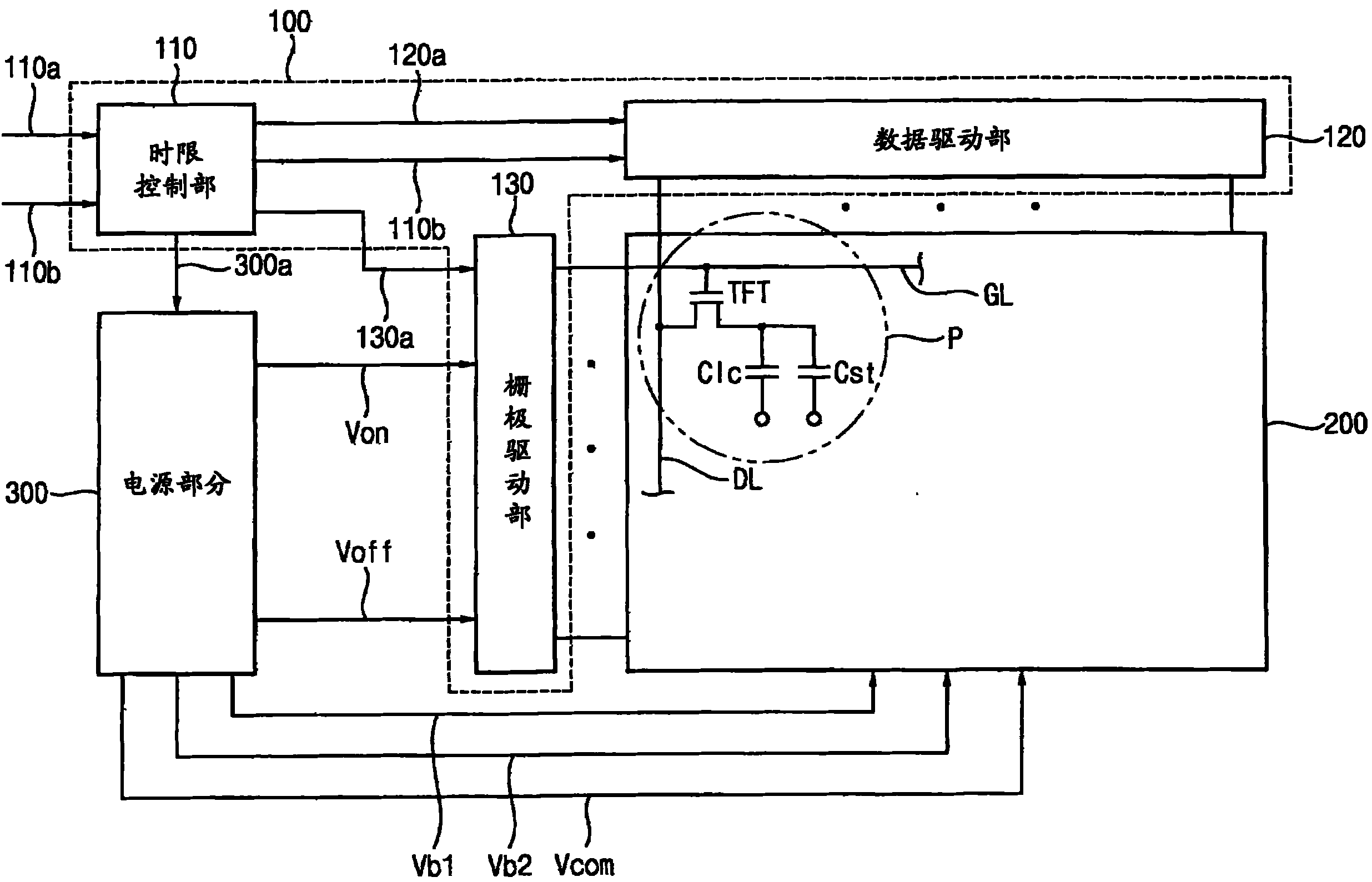
图1是示出了根据本发明示例性实施例的液晶显示器(LCD)装置的框图;1 is a block diagram illustrating a liquid crystal display (LCD) device according to an exemplary embodiment of the present invention;
图2是示出了图1中LCD面板的第一基板的平面图;2 is a plan view showing a first substrate of the LCD panel in FIG. 1;
图3是示出了沿图2的线I-I′截取的LCD面板的截面图;3 is a cross-sectional view showing the LCD panel taken along line II' of FIG. 2;
图4A是示出了图3中LCD面板的瞬时倾斜态的概念图;FIG. 4A is a conceptual diagram illustrating an instantaneous tilt state of the LCD panel in FIG. 3;
图4B是示出了图3中LCD面板的弯曲态的概念图;FIG. 4B is a conceptual diagram illustrating a bent state of the LCD panel in FIG. 3;
图5是示出了图1中电源部分的示意性框图;Fig. 5 is a schematic block diagram showing a power supply part in Fig. 1;
图6是示出了图1中LCD装置的驱动状态的时限图表;FIG. 6 is a time chart showing the driving state of the LCD device in FIG. 1;
图7是示出了校准时间间隔中的LCD面板的等效电路图;以及FIG. 7 is an equivalent circuit diagram showing an LCD panel in a calibration time interval; and
图8是示出了正常操作时间间隔中的LCD面板的等效电路图。FIG. 8 is an equivalent circuit diagram showing an LCD panel in a normal operation time interval.
具体实施方式Detailed ways
在附图中,为了清楚起见,层和区域的尺寸及相对尺寸可被放大。可以理解,当指出一个元件或层“位于”、“连接至”或“耦合至”另一元件或层时,它可以直接位于、连接至或耦合至另一元件或层上,或者可以存在插入的元件或层。相反,当指出一个元件“直接位于”、“直接连接至”或“直接耦合至”另一元件或层时,则不存在插入的元件或层。相同的标号通篇表示相同的元件。当用在本文中时,术语“和/或”包括一个或多个相关所列条目中的任一个以及所有组合。In the drawings, the size and relative sizes of layers and regions may be exaggerated for clarity. It will be understood that when an element or layer is referred to as being "located on," "connected to" or "coupled to" another element or layer, it can be directly on, connected to, or coupled to the other element or layer or intervening elements may be present. elements or layers. In contrast, when an element is referred to as being "directly on," "directly connected to" or "directly coupled to" another element or layer, there are no intervening elements or layers present. Like reference numerals refer to like elements throughout. As used herein, the term "and/or" includes any and all combinations of one or more of the associated listed items.
为了易于描述,本文可以使用空间相对关系术语,例如“下面”、“下方”、“下部”、“上方”、“上部”及类似词,以描述附图所示的一个元件或特征相对于另一个元件或特征的关系。可以理解,除了包括图中示出的方位外,空间相对关系术语还旨在包括装置在使用或操作中的不同方位。例如,如果将附图中的装置翻转,那么被描述为在其它元件或特征“下方”或“下面”的元件将被定位在其它元件或特征的“上方”。因此,示例性术语“下方”可以包括“上方”和“下方”两个方位。可以将装置以其它方式定位(旋转90°或处于其它方位),并且相应地对此处使用的空间相对关系术语进行解释。For ease of description, spatially relative terms, such as "below", "below", "lower", "above", "upper" and similar words may be used herein to describe the relative relation of one element or feature shown in the drawings to another. A relationship of a component or feature. It will be understood that the spatially relative terms are intended to encompass different orientations of the device in use or operation in addition to the orientation depicted in the figures. For example, if the device in the figures is turned over, elements described as "below" or "beneath" other elements or features would then be oriented "above" the other elements or features. Thus, the exemplary term "below" can encompass both an orientation of "above" and "beneath". The device may be otherwise oriented (rotated 90° or at other orientations) and the spatially relative terms used herein interpreted accordingly.
这里所使用的术语仅用于描述特定实施例的目的,而并不用于限制本发明。除非文中清楚地指明是其它情况,否则这里所使用的单数形式“一个”(“a”“an”和“the”)也旨在包括复数形式。还可以理解,当术语“包含(comprises和/或comprising)”用于本说明书中时,表明存在所述的特征、整体、步骤、操作、元件、和/或部件,但并不排除一个或多个其它的特征、整体、步骤、操作、元件、部件、和/或其组合的存在或附加。The terminology used herein is for the purpose of describing particular embodiments only and is not intended to be limiting of the invention. As used herein, the singular form "a", "an" and "the" is intended to include the plural forms as well, unless the context clearly dictates otherwise. It can also be understood that when the term "comprising (comprises and/or comprising)" is used in this specification, it indicates the presence of the described features, integers, steps, operations, elements, and/or components, but does not exclude one or more the presence or addition of one or more other features, integers, steps, operations, elements, parts, and/or combinations thereof.
以下,将参照作为本发明理想化实施例(和中间结构)的示意图的横截面图,描述本发明的实施例。因此,可以预料到由于例如制造技术和/或公差而造成的与图示形状的偏离。因此,本发明的实施例不应该被理解为局限于这里所示区域的特定形状,而是应该包括例如由于制造而产生的形状上的偏差。例如,图示为矩形的注入区通常在其边缘具有圆形的或弯曲的特征和/或注入浓度梯度,而不是从注入区到非注入区的二元变化。同样,通过注入形成的掩埋区可能在掩埋区与通过其发生注入的表面之间的区域中产生一些注入。因此,图中所示的区域实际上是示意性的,它们的形状不旨在描述装置区域的实际形状,并且也不旨在限制本发明的范围。Embodiments of the invention are described below with reference to cross section illustrations that are schematic illustrations of idealized embodiments (and intermediate structures) of the invention. Accordingly, deviations from the illustrated shapes as a result, for example, of manufacturing techniques and/or tolerances are to be expected. Thus, embodiments of the invention should not be construed as limited to the particular shapes of regions illustrated herein but are to include deviations in shapes that result, for example, from manufacturing. For example, an implanted region illustrated as a rectangle will, typically, have rounded or curved features and/or a gradient of implant concentration at its edges rather than a binary change from implanted to non-implanted region. Also, a buried region formed by implantation may generate some implantation in the region between the buried region and the surface through which the implantation occurs. Thus, the regions shown in the figures are schematic in nature and their shapes are not intended to illustrate the actual shape of a region of a device and are not intended to limit the scope of the invention.
图1是示出了根据本发明示例性实施例的液晶显示器(LCD)装置的框图。图2是示出了图1中LCD面板的第一基板的平面图。图3是示出了沿图2的线I-I′截取的LCD面板的截面图。图4A是示出了图3中LCD面板的瞬时倾斜态的概念图。图4B是示出了图3中LCD面板的弯曲态的概念图。FIG. 1 is a block diagram illustrating a liquid crystal display (LCD) device according to an exemplary embodiment of the present invention. FIG. 2 is a plan view illustrating a first substrate of the LCD panel in FIG. 1. Referring to FIG. FIG. 3 is a cross-sectional view showing the LCD panel taken along line II' of FIG. 2 . FIG. 4A is a conceptual diagram illustrating an instantaneous tilt state of the LCD panel in FIG. 3 . FIG. 4B is a conceptual diagram illustrating a bent state of the LCD panel in FIG. 3 .
参照图1,根据本发明示例性实施例的LCD装置100包括驱动部分100、显示图像的LCD面板200、以及为LCD面板200提供用于驱动LCD面板200的电力的电源部分300。Referring to FIG. 1 , an
驱动部分100包括时限控制部110、数据驱动部120和栅极驱动部130。The driving
时限控制部110接收来自于外部装置(诸如图形控制器等)的时限控制信号110a和数据信号110b。例如,时限控制信号110a可包括垂直同步信号(Vsync)、水平同步信号(Hsync)、主时钟信号(MCLK)、以及数据使能信号(DE)。垂直同步信号(Vsync)表示显示一个帧所需的时间。水平同步信号(Hsync)表示显示一行帧所需的时间。因此,水平同步信号(Hsync)包括了与包含在一行中的像素数量相对应的脉冲。数据使能信号(DE)表示向像素供应数据所需的时间。The
时限控制部110响应于控制信号110a而产生用于驱动数据驱动部120和栅极驱动部130的各种控制信号,并将所产生的控制信号输出到数据驱动部120和栅极驱动部130。例如,时限控制部110将数据控制信号120a输出到数据驱动部120,并且将栅极控制信号130a输出到栅极驱动部130。数据控制信号120a可包括载荷信号、水平启动信号和用于输出数据信号110b的极性控制信号。栅极控制信号130a可包括栅极时钟信号(GCLK)和垂直启动信号(STV)。此外,时限控制部110将电力控制信号300a输出到电源部分300。The
数据驱动部120设在LCD面板200的第一侧处。数据驱动部120响应于数据控制信号120a,将数据信号110b转换为模拟数据电压,并将模拟数据电压输出到LCD面板200。The
栅极驱动部130设在LCD面板200的第二侧处。栅极驱动部130响应于栅极控制信号130a,向LCD面板200提供从电源部分300供应的接通电压Von或断开电压Voff。The
LCD面板200响应于时限控制部110的控制,使用从电源部分300供应的电力显示图像。The
参照图3、图4A和图4B,LCD面板200包括第一基板210、面对第一基板210的第二基板220、以及介于第一基板210与第二基板220之间的光学补偿双折射(OCB)模式液晶层230。Referring to FIG. 3 , FIG. 4A and FIG. 4B , the
如图4A所示,OCB模式液晶层230在不大于临界电压下沿第一基板210与第二基板220之间形成的校准层(未示出)的校准方向保持瞬时倾斜态,即初始校准态。在瞬时倾斜态的液晶层230中,液晶分子排列在分别形成于第一基板210与第二基板220上的每个校准层上。邻近于校准层的液晶分子具有约2°至约5°的预倾斜角。液晶分子相对于液晶层230的中央部分以左右对称的方式布置,因此在液晶层230的中央部分中预倾斜角大约为0°。As shown in FIG. 4A, the OCB mode
如图4B所示,瞬时倾斜态的液晶层230在大于临界电压下转变为弯曲态。在弯曲态的液晶层230中,液晶分子排列在形成于第一基板210与第二基板220上的每个校准层上。邻近于校准层的液晶分子具有约2°至约5°的预倾斜角。液晶分子相对于液晶层230的中央部分以左右对称的方式布置,因此在液晶层230的中央部分中预倾斜角大约为90°。弯曲态的液晶层230具有这样的特征,即,透光率随着增加电压而线性地降低。As shown in FIG. 4B , the
因此,具有OCB模式液晶层230的LCD装置以校准时间间隔和正常操作时间间隔被操纵。在校准时间间隔期间,液晶层230从瞬时倾斜态转变为弯曲态,而在正常操作时间间隔期间,使用弯曲态的液晶层230来显示图像。Accordingly, the LCD device having the OCB mode
当施加于OCB模式液晶层230的电场增加时,从瞬时倾斜态到弯曲态的转换相对较快。因此,在第一基板210与第二基板220之间存在电压差,从而可降低液晶层230的转变速度。When the electric field applied to the OCB mode
参照图2和图3,第一基板210包括多个栅极线GL、多个数据线DL、以及多个像素区域P。数据线DL与栅极线GL交叉,使得数据线DL与栅极线GL绝缘。相邻的两条栅极线和相邻的两条数据线限定了像素区域P。每个像素区域P均包括:电连接于栅极线GL和数据线DL的薄膜晶体管(TFT)、电连接于TFT的液晶电容器CLc、以及电连接于TFT的存储电容器Cst。Referring to FIGS. 2 and 3 , the
栅极线GL形成在绝缘层211上,以限定像素区域P的上部和下部。栅极绝缘层212形成在其上形成有栅极线的绝缘基板211上,以覆盖栅极线GL。在一个实施例中,栅极绝缘层212包括氮化硅层(SiNx)或者氧化硅层(SiOx),尽管其他适合的绝缘层也在这些实施例的范围内。The gate line GL is formed on the insulating
数据线DL形成在栅极绝缘层212上,以限定像素区域P的上部和下部。The data line DL is formed on the
TFT形成在像素区域P内并且与栅极线GL和数据线DL电连接。TFT响应于通过栅极线GL提供的栅极信号,将通过数据线DL提供的数据电压施加给像素区域P的像素电极218。TFTs are formed in the pixel region P and are electrically connected to the gate line GL and the data line DL. The TFT applies a data voltage supplied through the data line DL to the
TFT包括栅电极213、激活层214、源电极215和漏电极216。The TFT includes a
栅电极213与栅极线GL电连接,以限定TFT的栅极端子。The
激活层214形成在栅极绝缘层212上,以覆盖栅电极213。激活层214可包括半导体层214a和欧姆接触层214b。例如,半导体层214a可包括非晶硅(a-Si),而欧姆接触层214b可包括n+非晶硅(n+a-Si)。在一个示例性实施例中,n+杂质以高浓度被注入到非晶硅层(a-Si),以形成欧姆接触层214b。The
源电极215形成在激活层214上,以与数据线DL电连接,从而形成TFT的源极端子。漏电极216形成在激活层214上,以与源电极215电绝缘,从而形成TFT的漏极端子。漏电极216通过形成在保护层217上的接触孔CNT与像素电极218电连接。源电极215和漏电极216在激活层214上相互分隔开,从而形成了TFT的信道(channel)。The
保护层217形成在其上形成有数据线DL的绝缘基板221上。保护层217包括例如氮化硅层(SiNx)或者氧化硅层(SiOx)。The
像素电极218对应于每一个像素区域P,形成在保护层217上。像素电极218包括光学透明材料和导电材料,以便传送光。例如,像素电极218包括氧化铟锌(IZO)、氧化铟锡(ITO)等。像素电极218通过形成在保护层217上的接触孔CNT与漏电极216电连接。The
第一基板210还包括存储电极219,以形成存储电容器Cst。存储电极219与存储线SL电连接,并且形成在像素区域P内。存储电极219和存储线SL由与栅极线GL和栅电极213相同的层和材料同时形成。可替换地,存储电极219和存储线SL可由与数据线DL相同的层和材料同时形成。The
存储电极219通过栅极绝缘层212和保护层217与像素电极218相对,从而形成存储电容器Cst。在一帧时间间隔期间,通过TFT施加给像素电极218的数据电压由存储电容器Cst保持。The
第二基板220通过液晶层230与第一基板210相对。第二基板220包括绝缘基板221和形成在绝缘基板221上的共用电极222。可替换地,第二基板220还可包括滤色层,以显现颜色。The
共用电极222包括光学透明材料和导电材料,以便传送光。例如,共用电极222可包括氧化铟锌(IZO)、氧化铟锡(ITO)等。共用电极222、像素电极218和液晶层230限定了液晶电容器CLc。The
在具有上述结构的LCD面板200中,根据被施加给共用电极222、像素电极218和存储电极219的电压,液晶层230的校准状态被转变。In the
参照图1和图3,电源部分300输出电源电压,以响应于时限控制部分110激活LCD面板200。Referring to FIGS. 1 and 3 , the
电源部分300为共用电极222和存储电极219提供共用电压Vcom,以在LCD面板200显示图像的正常操作状态下形成液晶电容器Clc和存储电容器Cst。The
电源部分300在校准时间间隔中为共用电极222提供高于施加给像素电极218的数据电压的第一校准电压Vb1,并且为存储电极219提供低于数据电压Vp的第二校准电压Vb2,在校准时间间隔期间液晶层230从瞬时倾斜态转变为弯曲态。例如,在第一校准电压Vb1和第二校准电压Vb2之间的电压差对于液晶层230的转变可至少为20V。The
如上所述,当高于像素电压Vp的较高电压被施加给位于液晶层230的上部中的共用电极222,并且低于像素电压Vp的较低电压被施加给位于液晶层230的下部中的存储电极219时,液晶层230的两个端部之间的电压差减小,使得液晶层230的转变速度减小。As described above, when a higher voltage higher than the pixel voltage Vp is applied to the
图5是示出了图1中的电源部分的示意性框图。图6是示出了图1中的LCD装置的驱动态的时限图表。图7是示出了在一个校准时间间隔中的LCD面板的等效电路图。图8是示出了在正常操作时间间隔中的等效电路图。FIG. 5 is a schematic block diagram showing a power supply section in FIG. 1 . FIG. 6 is a timing chart showing a driving state of the LCD device in FIG. 1. Referring to FIG. FIG. 7 is an equivalent circuit diagram showing an LCD panel in one calibration time interval. FIG. 8 is an equivalent circuit diagram showing an interval of normal operation.
参照图3、图5和图6,电源部分300可包括第一校准电压产生部310、第二校准电压产生部320、共用电压产生部330、第一切换部340、以及第二切换部350。Referring to FIGS. 3 , 5 and 6 , the
第一校准电压产生部310产生高于数据电压Vp的第一校准电压Vb1,之后向LCD面板200提供第一校准电压Vb1。例如,第一校准电压Vb1可为大约18V至大约20V。特别地,第一校准电压Vb1可为大约20V。The first calibration
第二校准电压产生部320产生低于第一校准电压Vb1和数据电压Vp的第二校准电压Vb2,之后向LCD面板200提供第二校准电压Vb2。例如,第二校准电压Vb2可为大约-3V至大约-7V。特别地,第二校准电压Vb2可为大约-5V。The second calibration
共用电压产生部330产生与数据电压Vp波动的平均值相对应的共用电压Vcom,之后向LCD面板200提供共用电压Vcom。例如,数据电压Vp在第一校准电压Vb1与第二校准电压Vb2之间波动。这里,共用电压Vcom可为大约5V至大约9V。特别地,共用电压Vcom可为大约7V。The common
第一切换部340响应于时限控制部110提供的电力控制信号300a,任意选择第一校准电压Vb1和共用电压Vcom中的一个,并向共用电极222提供所选的信号。为了如上所述执行操作,第一切换部340的第一部分任选地连接于第一校准电压产生部310和共用电压产生部330,并且第一切换部340的第二部分电连接于共用电极222。The
第二切换部350响应于时限控制部110提供的电力控制信号300a,任意选择第二校准电压Vb2和共用电压Vcom中的一个,并向存储电极219提供所选的信号。为了如上所述执行操作,第二切换部350的第一部分任选地连接于第二校准电压产生部320和共用电压产生部330,并且第二切换部350的第二部分电连接于存储电极219。The
如图7所示,在液晶分子从倾斜态转变为弯曲态的校准时间间隔期间,第一切换部340和第二切换部350分别电连接于第一校准电压产生部310和第二校准电压产生部320。As shown in FIG. 7 , during the calibration time interval when the liquid crystal molecules change from a tilted state to a bent state, the
因此,在校准时间间隔期间,从第一校准电压产生部310中提供的第一校准电压Vb1被施加给共用电极222,从第二校准电压产生部320中提供的第二校准电压Vb2被施加给存储电极219,如图6所示。施加给像素电极218的数据电压Vp基于共用电压Vcom在第一校准电压Vb1与第二校准电压Vb2之间波动。可替换地,在校准时间间隔期间,施加给像素电极218的数据电压Vp可相对地低于共用电压Vcom(即,约为0V)。Therefore, during the calibration time interval, the first calibration voltage Vb1 supplied from the first calibration
例如,当施加给共用电极222的第一校准电压Vb1为大约20V,并且施加给像素电极218的数据电压Vp在约0V至约14V之间波动时,在液晶层230的两端部分处产生约6V至约20V的电压差。然而,当约-5V的第二校准电压Vb2被施加给存储电极219时,在液晶层230的两端部分处产生最大约25V的电压差。因此,通过向存储电极219施加第二校准电压Vb2而增加液晶层230的两端部分之间的电压差,从而可提高液晶层230的转变速度。For example, when the first calibration voltage Vb1 applied to the
如图8所示,在液晶分子保持弯曲态的正常操作时间间隔期间,第一切换部340和第二切换部350电连接于共用电压产生部330。As shown in FIG. 8 , during a normal operation time interval when the liquid crystal molecules maintain a bent state, the
因此,在正常操作时间间隔期间,从共用电压产生部330提供的共用电压Vcom被施加给共用电极222和存储电极219,如图6所示。施加给像素电极218的数据电压Vp基于共用电压Vcom波动。Therefore, during the normal operation time interval, the common voltage Vcom supplied from the common
例如,当施加给共用电极222和存储电极219的共用电压Vcom为大约7V时,施加给像素电极218的数据电压Vp基于共用电压Vcom在约0V至约14V之间波动。For example, when the common voltage Vcom applied to the
像素电极218、共用电极222、以及介于像素电极218与共用电极222之间的液晶层230限定出液晶电容器CLc。像素电极218、存储电极219、以及介于像素电极218与存储电极219之间的栅极绝缘层212和保护层217限定出存储电容器Cst。液晶层230的校准状态通过像素电极218的数据电压Vp和共用电极222的共用电压Vcom而转变,因此通过使用在一个帧间隔期间保持校准状态的方法来正常显示图像。The
参照图1和图5,电源部分300可进一步包括栅极电压产生部360。栅极电压产生部360产生用于控制TFT的接通电压Von和断开电压Voff,之后向LCD面板200的栅极线GL提供接通电压Von和断开电压Voff。Referring to FIGS. 1 and 5 , the
接通电压Von是用于接通TFT的电压,断开电压Voff是用于断开TFT的电压。接通电压Von和断开电压Voff响应于时限控制部110,通过栅极驱动部130被施加给LCD面板200的栅极线GL。例如,接通电压Von可以为大约18V至大约22V,断开电压Voff可以为大约-3V至大约-7V。The on voltage Von is a voltage for turning on the TFT, and the off voltage Voff is a voltage for turning off the TFT. The on voltage Von and the off voltage Voff are applied to the gate lines GL of the
从栅极电压产生部360中产生的接通电压Von基本上等于从第一校准电压产生部310中产生的第一校准电压Vb1,从栅极电压产生部360中产生的断开电压Voff基本上等于从第二校准电压产生部320中产生的第二校准电压Vb2。The on-voltage Von generated from the gate
因此,当接通电压Von和断开电压Voff分别用作第一校准电压Vb1和第二校准电压Vb2时,第一校准电压产生部310和第二校准电压产生部320可被省却,从而可简化电源部分300。Therefore, when the on voltage Von and the off voltage Voff are respectively used as the first calibration voltage Vb1 and the second calibration voltage Vb2, the first calibration
根据LCD装置和驱动LCD装置的方法,低于共用电压的校准电压被施加给存储电极,从而提高OCB模式液晶分子从瞬时倾斜态转变为弯曲态的转变速度。因此,可减少校准时间间隔,从而提高显示质量。According to the LCD device and the method of driving the LCD device, a calibration voltage lower than a common voltage is applied to the storage electrode, thereby increasing a transition speed of liquid crystal molecules in an OCB mode from an instantaneous tilted state to a bent state. Therefore, the calibration time interval can be reduced, thereby improving the display quality.
尽管已描述了本发明的示例性实施例,但是应该理解的是,本发明不应局限于这些示例性实施例,在所附权利要求限定的本发明精神和保护范围内,本领域中普通技术人员可作出各种改变和修正。Although the exemplary embodiments of the present invention have been described, it should be understood that the present invention should not be limited to these exemplary embodiments. Various changes and modifications may be made by personnel.
Claims (9)
Applications Claiming Priority (3)
| Application Number | Priority Date | Filing Date | Title |
|---|---|---|---|
| KR10-2006-0066659 | 2006-07-18 | ||
| KR1020060066659 | 2006-07-18 | ||
| KR1020060066659A KR101189090B1 (en) | 2006-07-18 | 2006-07-18 | LCD and its driving method |
Publications (2)
| Publication Number | Publication Date |
|---|---|
| CN101110201A CN101110201A (en) | 2008-01-23 |
| CN101110201B true CN101110201B (en) | 2011-09-07 |
Family
ID=38971098
Family Applications (1)
| Application Number | Title | Priority Date | Filing Date |
|---|---|---|---|
| CN2007101294534A Expired - Fee Related CN101110201B (en) | 2006-07-18 | 2007-07-17 | Liquid crystal display device and method of driving the same |
Country Status (4)
| Country | Link |
|---|---|
| US (1) | US8077127B2 (en) |
| JP (1) | JP4862184B2 (en) |
| KR (1) | KR101189090B1 (en) |
| CN (1) | CN101110201B (en) |
Families Citing this family (2)
| Publication number | Priority date | Publication date | Assignee | Title |
|---|---|---|---|---|
| JP5639060B2 (en) | 2008-09-04 | 2014-12-10 | イーエルシー マネージメント エルエルシー | Objective model, method and use of apparent age |
| CN109164862A (en) * | 2018-07-24 | 2019-01-08 | 惠科股份有限公司 | Reference voltage generation system and generation method |
Citations (5)
| Publication number | Priority date | Publication date | Assignee | Title |
|---|---|---|---|---|
| US20020057247A1 (en) * | 2000-11-10 | 2002-05-16 | Lee Chang Hun | LCD for speeding initial bend state, driver and method thereof |
| US6542211B1 (en) * | 1998-06-18 | 2003-04-01 | Canon Kabushiki Kaisha | Liquid crystal device and driving method therefor |
| CN1428761A (en) * | 2001-12-27 | 2003-07-09 | Lg.飞利浦Lcd有限公司 | Equipment and method for driving liquid crystal display |
| CN1550862A (en) * | 2003-05-13 | 2004-12-01 | 三星电子株式会社 | LCD Monitor |
| US20050052396A1 (en) * | 2003-09-05 | 2005-03-10 | Kim Myeong-Su | Liquid crystal display |
Family Cites Families (6)
| Publication number | Priority date | Publication date | Assignee | Title |
|---|---|---|---|---|
| JP3074640B2 (en) * | 1995-12-22 | 2000-08-07 | インターナショナル・ビジネス・マシーンズ・コーポレ−ション | Driving method of liquid crystal display device |
| JPH10104087A (en) | 1996-09-27 | 1998-04-24 | Yokogawa Electric Corp | Liquid crystal display |
| JP3967577B2 (en) * | 2001-10-19 | 2007-08-29 | 東芝松下ディスプレイテクノロジー株式会社 | Method for driving liquid crystal panel and liquid crystal display device |
| JP2003255389A (en) * | 2002-03-06 | 2003-09-10 | Matsushita Electric Ind Co Ltd | Liquid crystal display |
| JP3959291B2 (en) * | 2002-03-19 | 2007-08-15 | 東芝松下ディスプレイテクノロジー株式会社 | Method for driving liquid crystal panel and liquid crystal display device |
| TWI329216B (en) * | 2006-01-02 | 2010-08-21 | Chunghwa Picture Tubes Ltd | Pixel structure and liquid crystal display panel |
-
2006
- 2006-07-18 KR KR1020060066659A patent/KR101189090B1/en not_active Expired - Fee Related
-
2007
- 2007-07-11 US US11/776,446 patent/US8077127B2/en not_active Expired - Fee Related
- 2007-07-17 CN CN2007101294534A patent/CN101110201B/en not_active Expired - Fee Related
- 2007-07-17 JP JP2007185156A patent/JP4862184B2/en not_active Expired - Fee Related
Patent Citations (5)
| Publication number | Priority date | Publication date | Assignee | Title |
|---|---|---|---|---|
| US6542211B1 (en) * | 1998-06-18 | 2003-04-01 | Canon Kabushiki Kaisha | Liquid crystal device and driving method therefor |
| US20020057247A1 (en) * | 2000-11-10 | 2002-05-16 | Lee Chang Hun | LCD for speeding initial bend state, driver and method thereof |
| CN1428761A (en) * | 2001-12-27 | 2003-07-09 | Lg.飞利浦Lcd有限公司 | Equipment and method for driving liquid crystal display |
| CN1550862A (en) * | 2003-05-13 | 2004-12-01 | 三星电子株式会社 | LCD Monitor |
| US20050052396A1 (en) * | 2003-09-05 | 2005-03-10 | Kim Myeong-Su | Liquid crystal display |
Also Published As
| Publication number | Publication date |
|---|---|
| JP4862184B2 (en) | 2012-01-25 |
| KR101189090B1 (en) | 2012-11-09 |
| US8077127B2 (en) | 2011-12-13 |
| JP2008026899A (en) | 2008-02-07 |
| US20080018813A1 (en) | 2008-01-24 |
| CN101110201A (en) | 2008-01-23 |
| KR20080007699A (en) | 2008-01-23 |
Similar Documents
| Publication | Publication Date | Title |
|---|---|---|
| TWI262467B (en) | Liquid crystal display and driving method thereof | |
| JP4359631B2 (en) | Method and apparatus for driving liquid crystal display device | |
| KR101243789B1 (en) | LCD and drive method thereof | |
| TWI415094B (en) | Liquid crystal display device | |
| US7764262B2 (en) | Liquid crystal display device and method of driving the same | |
| US9323123B2 (en) | Structure of pixel | |
| US9530384B2 (en) | Display device that compensates for changes in driving frequency and drive method thereof | |
| TW554324B (en) | Liquid crystal display drive method and liquid crystal display | |
| JP2010026393A (en) | Driving method of liquid crystal display device and liquid crystal display device | |
| JP4633669B2 (en) | Liquid crystal display device and driving method thereof | |
| US8823891B2 (en) | Bi-stable chiral splay nematic mode liquid crystal display device and method of driving the same | |
| CN101110201B (en) | Liquid crystal display device and method of driving the same | |
| JP4528598B2 (en) | Liquid crystal display | |
| JP5035888B2 (en) | Liquid crystal display device and driving method of liquid crystal display device | |
| KR102270257B1 (en) | Display device and driving method for display device using the same | |
| KR20130065328A (en) | Electrophoresis display apparatus and method for driving the same | |
| KR101327875B1 (en) | LCD and drive method thereof | |
| US20120105419A1 (en) | Driving Circuit for Liquid Crystal Pixel Array and Liquid Crystal Display Using the Same | |
| CN104081447A (en) | Liquid crystal display device and liquid crystal display device driving method | |
| JP2010008576A (en) | Liquid crystal display, and method of driving liquid crystal display | |
| JP4722562B2 (en) | LCD panel | |
| KR20070115537A (en) | LCD and its driving method | |
| KR100730175B1 (en) | Transition driving method and apparatus thereof for OCC liquid crystal display panel | |
| KR20070079187A (en) | LCD Display | |
| KR20070059685A (en) | Transition driving method and apparatus thereof for OCC liquid crystal display panel |
Legal Events
| Date | Code | Title | Description |
|---|---|---|---|
| C06 | Publication | ||
| PB01 | Publication | ||
| C10 | Entry into substantive examination | ||
| SE01 | Entry into force of request for substantive examination | ||
| C14 | Grant of patent or utility model | ||
| GR01 | Patent grant | ||
| ASS | Succession or assignment of patent right |
Owner name: SAMSUNG DISPLAY CO., LTD. Free format text: FORMER OWNER: SAMSUNG ELECTRONICS CO., LTD. Effective date: 20121228 |
|
| C41 | Transfer of patent application or patent right or utility model | ||
| TR01 | Transfer of patent right |
Effective date of registration: 20121228 Address after: Gyeonggi Do, South Korea Patentee after: Samsung Display Co.,Ltd. Address before: Gyeonggi Do, South Korea Patentee before: Samsung Electronics Co.,Ltd. |
|
| CF01 | Termination of patent right due to non-payment of annual fee |
Granted publication date: 20110907 Termination date: 20200717 |
|
| CF01 | Termination of patent right due to non-payment of annual fee |