CN101026335B - Control circuit for power supply device, power supply device, and control method thereof - Google Patents
Control circuit for power supply device, power supply device, and control method thereof Download PDFInfo
- Publication number
- CN101026335B CN101026335B CN2006100875032A CN200610087503A CN101026335B CN 101026335 B CN101026335 B CN 101026335B CN 2006100875032 A CN2006100875032 A CN 2006100875032A CN 200610087503 A CN200610087503 A CN 200610087503A CN 101026335 B CN101026335 B CN 101026335B
- Authority
- CN
- China
- Prior art keywords
- level
- voltage
- power supply
- initial
- supply device
- Prior art date
- Legal status (The legal status is an assumption and is not a legal conclusion. Google has not performed a legal analysis and makes no representation as to the accuracy of the status listed.)
- Expired - Fee Related
Links
Images


Classifications
-
- G—PHYSICS
- G11—INFORMATION STORAGE
- G11C—STATIC STORES
- G11C5/00—Details of stores covered by group G11C11/00
- G11C5/14—Power supply arrangements, e.g. power down, chip selection or deselection, layout of wirings or power grids, or multiple supply levels
-
- H—ELECTRICITY
- H02—GENERATION; CONVERSION OR DISTRIBUTION OF ELECTRIC POWER
- H02J—ELECTRIC POWER NETWORKS; CIRCUIT ARRANGEMENTS OR SYSTEMS FOR SUPPLYING OR DISTRIBUTING ELECTRIC POWER; SYSTEMS FOR STORING ELECTRIC ENERGY
- H02J7/00—Circuit arrangements for charging or discharging batteries or for supplying loads from batteries
- H02J7/34—Parallel operation in networks using both storage and other DC sources, e.g. providing buffering
Landscapes
- Engineering & Computer Science (AREA)
- Power Engineering (AREA)
- Dc-Dc Converters (AREA)
- Direct Current Feeding And Distribution (AREA)
Abstract
本发明提供了用于电源装置的控制电路、电源装置及其控制方法,其中要供应到各种设备的输出电压被高速而高效地确定并设定到最优电平。电源装置中的控制电路(10A)向设备(60)供应从V1到V3范围内的所需电压电平,所述设备提供初始电压,然后要求接收所需电压电平。控制电路(10A)包括用于接收诸如V1之类的要求电平的通信单元(21),以及包括REG1至REG3在内的用于预先存储用于确定初始电压的初始设定电平和通信单元(21)所接收的要求电平的存储单元(22)。从V1到V3范围内的初始电压或所需电压可以响应于初始设定电平或要求电平来控制。
The present invention provides a control circuit for a power supply device, a power supply device and a control method thereof, in which output voltages to be supplied to various devices are determined and set to optimum levels at high speed and efficiently. A control circuit (10A) in the power supply unit supplies a desired voltage level ranging from V1 to V3 to a device (60) which provides an initial voltage and then requires to receive the desired voltage level. The control circuit (10A) includes a communication unit (21) for receiving a desired level such as V1, and a communication unit including REG1 to REG3 for storing in advance an initial set level for determining an initial voltage and a communication unit ( 21) Storage unit (22) of the received request level. The initial or desired voltage ranging from V1 to V3 may be controlled in response to an initial set level or desired level.
Description
技术领域 technical field
本发明涉及用于电源装置的控制电路、电源,以及用于控制电源的方法。The present invention relates to a control circuit for a power supply device, a power supply, and a method for controlling the power supply.
背景技术 Background technique
由于集成电路(例如LSI或IC)通常在制造工艺上有所不同,因此其晶体管的阈值电压电平或电阻水平可能不一致。而且,取决于使用条件(包括周围温度),这种集成电路的晶体管的阈值电压电平或电阻水平可能不同。在晶体管的阈值电压电平或电阻水平不一致的情况下,集成电路的延迟时间将因此不同,从而操作速度也不同。为了消除操作速度上的任何显著变化,设置了电源装置,用于向集成电路施加与阈值电压电平或电阻水平相关的最优电压。Since integrated circuits such as LSIs or ICs generally vary in manufacturing process, their transistors may not have uniform threshold voltage levels or resistance levels. Also, the threshold voltage level or resistance level of transistors of such an integrated circuit may vary depending on usage conditions (including ambient temperature). In the event that the threshold voltage levels or resistance levels of the transistors are inconsistent, the delay time of the integrated circuit will therefore be different, and thus the operating speed will also be different. In order to eliminate any significant variation in operating speed, power supply means are provided for applying an optimum voltage to the integrated circuit in relation to the threshold voltage level or resistance level.
在日本未实审专利公开第2000-228833和2001-332695号中分别公开了电源装置控制的电子设备和集成电路。第2000-228833号公开的电子设备被设置为通过外部电源对其相关联的电池进行充电,并为操作系统组件而放电。具体而言,对其电源装置(电源)的输出进行控制,以使得系统组件的操作功率与对电池的充电的总和保持基本一定。该电子设备使得电源装置的控制器可以监控电源装置的输出(电流),并控制供应到系统组件的功率和对相关联的电池的充电,从而使功耗最小化。An electronic device and an integrated circuit controlled by a power supply unit are disclosed in Japanese Unexamined Patent Publication Nos. 2000-228833 and 2001-332695, respectively. The electronic device disclosed in Publication No. 2000-228833 is configured to charge its associated battery by an external power source and discharge it for operating system components. Specifically, the output of its power supply device (power supply) is controlled so that the sum of the operating power of the system components and the charging of the battery is kept substantially constant. The electronics allow a controller of the power supply unit to monitor the output (current) of the power supply unit and control power supplied to system components and charging of associated batteries to minimize power consumption.
第2001-332695号公开的集成电路包括第一逻辑门和第二逻辑门,所述第一逻辑门由电位差较小的第一组电位供电,所述第二逻辑门由电位差较大的第二组电位供电,而MIS晶体管处的参考电位由第一逻辑门和第二逻辑门共享。该集成电路使得第二逻辑门中的MIS晶体管的电压输出幅值变得大于第一逻辑门中的MIS晶体管的电压输出幅值,从而以高于第一逻辑门的速度来操作第二逻辑门。而且,由于集成电路中每个逻辑门的功耗与MIS晶体管的电压输出幅值的平方成比例,因此将第一逻辑门中的MIS晶体管的电压输出幅值设置为小于第二逻辑门中的MIS晶体管的电压输出幅值,从而可以利用比第二逻辑门更低的功耗来操作第一逻辑门。The integrated circuit disclosed in No. 2001-332695 includes a first logic gate and a second logic gate, the first logic gate is powered by a first group of potentials with a smaller potential difference, and the second logic gate is powered by a group of potentials with a larger potential difference The second set of potentials supplies power, while the reference potential at the MIS transistor is shared by the first logic gate and the second logic gate. The integrated circuit causes the voltage output magnitude of the MIS transistor in the second logic gate to become greater than the voltage output magnitude of the MIS transistor in the first logic gate, thereby operating the second logic gate at a higher speed than the first logic gate . Moreover, since the power consumption of each logic gate in the integrated circuit is proportional to the square of the voltage output amplitude of the MIS transistor, the voltage output amplitude of the MIS transistor in the first logic gate is set to be smaller than that in the second logic gate The voltage output amplitude of the MIS transistor, so that the first logic gate can be operated with lower power consumption than the second logic gate.
发明内容 Contents of the invention
电源装置与包括上述集成电路在内的各种设备相连接。因此,有必要将电源装置的输出电压修改到其最优电平以匹配于连接的设备,同时防止集成电路的操作速度由于晶体管阈值电压电平或电阻水平的任何不同而出现显著的不同。The power supply unit is connected to various devices including the above-mentioned integrated circuits. Therefore, it is necessary to modify the output voltage of the power supply unit to its optimum level to match the connected equipment, while preventing the operating speed of the integrated circuit from being significantly different due to any difference in transistor threshold voltage level or resistance level.
然而,电源装置的电压输出不得不在每次启动电源装置时被调节到最优电平。由于电压输出被从其固定的初始设定值修改为随着每个设备而不同的最优电平,因此其修改所需的时间将会被显著延长。换言之,难以高速地将电压输出修改到其最优电平。However, the voltage output of the power supply unit has to be adjusted to an optimal level every time the power supply unit is started up. As the voltage output is modified from its fixed initial set value to an optimal level that differs for each device, the time required for its modification will be significantly extended. In other words, it is difficult to modify the voltage output to its optimal level at high speed.
而且,电源装置允许其电压输出被根据所连接设备的每个类型而从固定的初始设定值修改到最优电平,因此其设定动作将是效率非常低的。Also, the power supply device allows its voltage output to be modified from a fixed initial setting value to an optimal level according to each type of connected equipment, so its setting action will be very inefficient.
本发明是考虑到以上缺点而设计的,其目的在于提供一种用于电源装置的控制电路、一种电源装置及其控制方法,其中可以高速而高效地将要供应到多种设备的电压输出设定为最优电平。The present invention is designed in consideration of the above disadvantages, and an object thereof is to provide a control circuit for a power supply device, a power supply device and a control method thereof, in which voltage output devices to be supplied to various devices can be quickly and efficiently set to the optimum level.
本发明第一技术方案的用于电源装置的控制电路,以及本发明第二技术方案的用于向提供初始电压然后要求接收不同于初始电压的所需电压的设备供应所需电压的电源装置包括:用于接收所需电压的要求电平的通信单元;以及用于预先存储用于确定初始电压的初始设定电平和存储通信单元所接收到的要求电平的存储单元,其中响应于初始设定电平或要求电平来控制初始电压或所需电压。The control circuit for the power supply device of the first technical solution of the present invention, and the power supply device for supplying the required voltage to the equipment that provides the initial voltage and then requires to receive the required voltage different from the initial voltage according to the second technical solution of the present invention include : a communication unit for receiving a required level of a required voltage; and a storage unit for pre-storing an initial set level for determining an initial voltage and storing the required level received by the communication unit, wherein in response to the initial setting Set level or required level to control initial voltage or desired voltage.
本发明第一技术方案的用于电源装置的控制电路,以及本发明第二技术方案的电源装置包括用于接收所需电压的要求电平的通信单元,以及用于预先存储用于确定初始电压的初始设定电平和存储通信单元所接收到的要求电平的存储单元,其中响应于初始设定电平或要求电平来控制初始电压或所需电压。结果,与每次电源装置启动时都将电压调节到设备的最优电平的情况相比,响应于存储在存储单元中的要求电平而直接将电压设定到所连接的设备所需的最优电平所需的时间可以变得更短。换言之,可以高效而高速的将要供应到设备的电压设定到最优电平。The control circuit for a power supply device according to the first technical aspect of the present invention, and the power supply device according to the second technical aspect of the present invention include a communication unit for receiving a required level of a required voltage, and a device for pre-storing The initially set level and the storage unit storing the required level received by the communication unit, wherein the initial voltage or the required voltage is controlled in response to the initially set level or the required level. As a result, compared with the case where the voltage is adjusted to the optimum level for the equipment each time the power supply unit is started, the voltage is directly set to the level required by the connected equipment in response to the required level stored in the storage unit. The time required for the optimum level can be made shorter. In other words, the voltage to be supplied to the device can be set to an optimum level efficiently and at high speed.
本发明第三技术方案的电源装置控制方法用于向提供初始电压然后要求接收不同于初始电压的所需电压的设备供应所需电压,该方法包括以下步骤:接收所需电压的要求电平;预先存储用于确定初始电压的初始设定电平,并存储所接收到的要求电平;以及响应于初始设定电平或要求电平来控制初始电压或所需电压。The power supply device control method of the third technical aspect of the present invention is for supplying a required voltage to a device that supplies an initial voltage and then requires receiving a required voltage different from the initial voltage, the method comprising the steps of: receiving a required level of the required voltage; storing in advance an initial set level for determining the initial voltage, and storing the received requested level; and controlling the initial voltage or the requested voltage in response to the initially set level or the requested level.
本发明第三技术方案的电源装置控制方法包括以下步骤:接收所需电压的要求电平;预先存储用于确定初始电压的初始设定电平,并存储所接收到的要求电平;以及响应于初始设定电平或要求电平来控制初始电压或所需电压。结果,与每次电源装置启动时都将电压调节到设备的最优电平的情况相比,响应于所存储的要求电平而直接将电压设定到所连接的设备所需的最优电平所需的时间可以变得更短。换言之,可以高效而高速的将要供应到设备的电压设定到最优电平。The power supply device control method of the third technical aspect of the present invention includes the steps of: receiving a required level of a required voltage; storing in advance an initial set level for determining an initial voltage, and storing the received required level; and responding The initial voltage or the required voltage is controlled at the initial set level or the required level. As a result, the voltage is directly set to the optimum level required by the connected equipment in response to the stored demand level, compared to the case where the voltage is adjusted to the optimum level for the equipment each time the power supply unit is started. The time required for leveling can be shortened. In other words, the voltage to be supplied to the device can be set to an optimum level efficiently and at high speed.
附图说明 Description of drawings
当结合附图来阅读时,从以下的详细描述中,本发明的上述及其它目的和新特征将会更充分地呈现出来。但是应当明确理解的是,附图仅用于说明性目的,而非意在定义对本发明的限定。The above and other objects and novel features of the present invention will appear more fully from the following detailed description when read in conjunction with the accompanying drawings. However, it should be clearly understood that the drawings are for illustrative purposes only, and are not intended to define limitations of the present invention.
图1是示出本发明第一实施例的电源装置和电子设备之间的连接的框图;FIG. 1 is a block diagram showing a connection between a power supply unit and electronic equipment according to a first embodiment of the present invention;
图2是连接到电子设备的电源装置的电路图;2 is a circuit diagram of a power supply unit connected to an electronic device;
图3是与电源装置相连的电子设备的示意图。Fig. 3 is a schematic diagram of electronic equipment connected to a power supply unit.
具体实施方式 Detailed ways
(实施例)(Example)
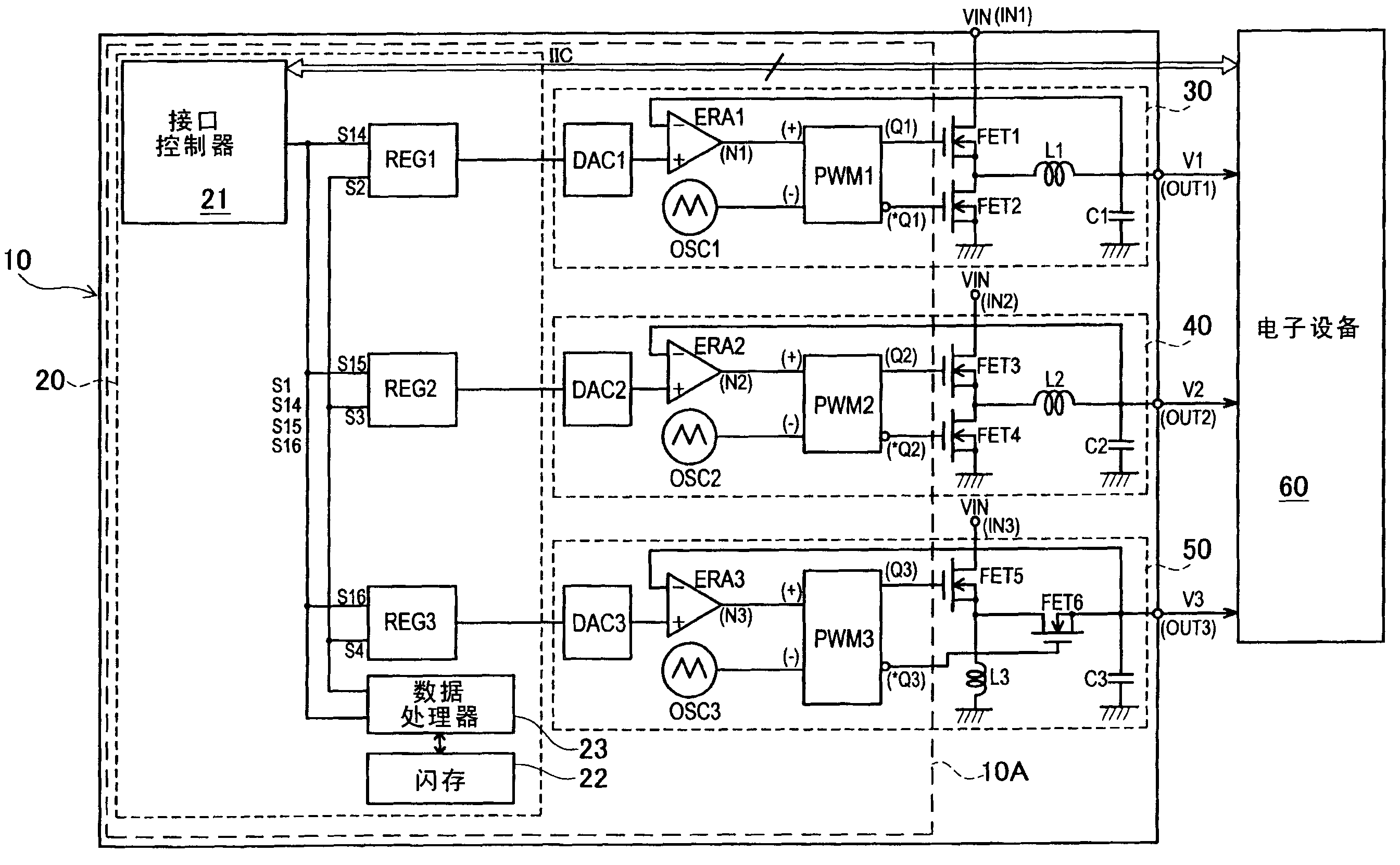
下面参照图1至3来描述本发明的一个实施例。如图1所示,该实施例的电源装置10通过IIC总线IIC(通信装置)连接到电子设备60(外部设备)。IIC总线IIC用于在电源装置10和电子设备60之间交换多种数据。如图所示,电源装置10具有三个(CH-1至CH-3)通道输出。电子设备60包括一个或多个集成电路。An embodiment of the present invention will be described below with reference to FIGS. 1 to 3 . As shown in FIG. 1, the
如图2所示,电源装置10包括通信控制器20,以及第一至第三DC-DC变换器30至50。通信控制器20包括接口控制器21、闪存22、数据处理器23(例如MPU),以及三个寄存器REG1至REG3。图中10A表示的是电源装置10的控制电路。As shown in FIG. 2 , the
接口控制器21与IIC总线IIC相连。从图2和3中可以看出,IIC总线IIC连接到电子设备60的接口控制器61。如图3所示,电子设备60包括环形振荡器RINGOSC和振荡器OSC4。环形振荡器RINGOSC和振荡器OSC4连接到锁相环电路PLL。锁相环电路PLL连接到频率/电压转换器63。频率/电压转换器63接着与接口控制器61相连。The
如图2所示,寄存器REG1、REG2和REG3以及数据处理器23与接口控制器21并联连接。闪存22连接到数据处理器23,数据处理器23又并联连接到寄存器REG1、REG2和REG3。As shown in FIG. 2 , the registers REG1 , REG2 and REG3 and the
如图所示,寄存器REG1连接到第一DC-DC变换器30的D/A转换器DAC1。寄存器REG2连接到第二DC-DC变换器40的D/A转换器DAC2。寄存器REG3连接到第三DC-DC变换器50的D/A转换器DAC3。The register REG1 is connected to the D/A converter DAC1 of the first DC-
如图所示,第一DC-DC变换器30包括主开关晶体管FET1、同步侧开关晶体管FET2、扼流圈L1和电容器C1。主开关晶体管FET1的漏极连接到输入端(IN1),用于接收直流输入电压VIN。如图3所示,直流输入电压VIN既施加到主开关晶体管FET1,又经由输入端(IN4)施加到通信控制器20。主开关晶体管FET1的源极连接到同步侧开关晶体管FET2的漏极。同步侧开关晶体管FET2的源极连接到地。而且,主开关晶体管FET1的源极和同步侧开关晶体管FET2的漏极连接到扼流圈L1。扼流圈L1连接到输出端(OUT1)。电容器C1连接在输出端(OUT1)和地之间。输出端(OUT1)连接到电子设备60。As shown in the figure, the first DC-
第一DC-DC变换器30还包括误差放大器ERA1、D/A转换器DAC1、三角波振荡器OSC1和PWM比较器PWM1。误差放大器ERA1的反相输入端连接到输出端(OUT1)。误差放大器ERA1的同相输入端连接到D/A转换器DAC1。The first DC-
三角波振荡器OSC1输出三角波信号。该三角波信号在一个电压幅值范围内(例如在1.0V到2.0V之间)振荡。三角波振荡器OSC1可以包括OP放大器、电阻器、电容器等等。The triangular wave oscillator OSC1 outputs a triangular wave signal. The triangular wave signal oscillates within a range of voltage amplitudes (eg, between 1.0V and 2.0V). The triangle wave oscillator OSC1 may include an OP amplifier, resistors, capacitors, and the like.
PWM比较器PWM1具有正输入端(+)和负输入端(-)。正输入端(+)连接到误差放大器ERA1的输出端(N1),而负输入端(-)连接到三角波振荡器OSC1。PWM比较器PWM1的输出端(Q1)连接到主开关晶体管FET1的栅极,并且PWM比较器PWM1的反相输出端(*Q1)连接到同步侧开关晶体管FET2的栅极。The PWM comparator PWM1 has a positive input terminal (+) and a negative input terminal (−). The positive input (+) is connected to the output (N1) of the error amplifier ERA1, and the negative input (-) is connected to the triangle wave oscillator OSC1. The output terminal (Q1) of the PWM comparator PWM1 is connected to the gate of the main switching transistor FET1, and the inverting output terminal (*Q1) of the PWM comparator PWM1 is connected to the gate of the synchronous side switching transistor FET2.
第二DC-DC变换器40在结构上与第一DC-DC变换器30基本相同。更具体而言,可以分别用误差放大器ERA2、D/A转换器DAC2、三角波振荡器OSC2、PWM比较器PWM2、主开关晶体管FET3、同步侧开关晶体管FET4、扼流圈L2和电容器C2来代替误差放大器ERA1、D/A转换器DAC1、三角波振荡器OSC1、PWM比较器PWM1、主开关晶体管FET1、同步侧开关晶体管FET2、扼流圈L1和电容器C1,从而构造出本实施例的第二DC-DC变换器40。三角波振荡器OSC2和三角波振荡器OSC1一样地输出在一个电压幅值范围内(例如在1.0V到2.0V之间)振荡的三角波信号。The second DC-
N2、IN2和OUT2分别表示的是误差放大器ERA2的输出端、第二DC-DC变换器40的输入端和第二DC-DC变换器40的输出端。PWM比较器PWM2的输出端和反相输出端分别用Q2和*Q2表示。输出端OUT2连接到电子设备60。N2 , IN2 and OUT2 represent the output terminal of the error amplifier ERA2 , the input terminal of the second DC-
第三DC-DC变换器50包括NMOS晶体管FET5、NMOS晶体管FET6、扼流圈L3和电容器C3。如图所示,NMOS晶体管FET5的漏极连接到输入端IN3,用于接收直流输入电压VIN。NMOS晶体管FET5的源极连接到扼流圈L3,该扼流圈L3又连接到地。The third DC-
NMOS晶体管FET5的源极连接到NMOS晶体管FET6的漏极。而且,NMOS晶体管FET6的源极连接到输出端OUT3。电容器C3连接在输出端OUT3和地之间。输出端OUT3连接到电子设备60。The source of the NMOS transistor FET5 is connected to the drain of the NMOS transistor FET6. Also, the source of the NMOS transistor FET6 is connected to the output terminal OUT3. Capacitor C3 is connected between output terminal OUT3 and ground. The output terminal OUT3 is connected to the
第三DC-DC变换器50包括误差放大器ERA3、D/A转换器DAC3、三角波振荡器OSC3和PWM比较器PWM3。误差放大器ERA3的反相输入端连接到输出端OUT3。误差放大器ERA3的同相输入端连接到D/A转换器DAC3。三角波振荡器OSC3和三角波振荡器OSC1及OSC2一样地输出三角波信号。The third DC-
PWM比较器PWM3的正输入端(+)连接到误差放大器ERA3的输出端N3,其负输入端(-)连接到三角波振荡器OSC3。PWM比较器PWM3的输出端Q3连接到NMOS晶体管FET5的栅极。PWM比较器PWM3的反相输出端*Q3连接到NMOS晶体管FET6的栅极。The positive input terminal (+) of the PWM comparator PWM3 is connected to the output terminal N3 of the error amplifier ERA3, and the negative input terminal (-) thereof is connected to the triangular wave oscillator OSC3. The output terminal Q3 of the PWM comparator PWM3 is connected to the gate of the NMOS transistor FET5. The inverting output terminal *Q3 of the PWM comparator PWM3 is connected to the gate of the NMOS transistor FET6.
现在描述电源装置10的控制方法。当图2所示的电源装置10通电时,其接口控制器21将复位信号S1输出到数据处理器23。当接收到复位信号S1时,数据处理器23访问闪存22以读取初始数据。该初始数据用于将电压V1设为在闪存22中预先存储于非易失模式的初始电平,所述电压V1要被供应到与第一DC-DC变换器30的输出端OUT1相连的电子设备60。更具体而言,初始电压被设为与本发明的初始设定电平相对应的电子设备60的额定电平(例如5V)。数据处理器23将与初始数据相对应的电压命令信号S2输出到寄存器REG1。由于闪存22以非易失模式存储初始数据(初始设定电平),其对应于本发明的非易失性存储装置(存储器)。初始设定电平不局限于电子设备60的额定电平(5V),而是可以从额定电压的允许范围(例如从4.5V到5.5V)中选择。A control method of the
寄存器REG1存储电压命令信号S2,然后将信号S2输出到第一DC-DC变换器30的D/A转换器DAC1。当电源装置10通电时,寄存器REG1以易失模式存储初始数据(初始设定电平)的电压命令信号S2,并且对应于本发明的寄存器单元(易失性存储单元)。The register REG1 stores the voltage command signal S2 and then outputs the signal S2 to the D/A converter DAC1 of the first DC-
D/A转换器DAC1从电压命令信号S2产生模拟电压信号(参考电压),该模拟电压信号然后被误差放大器ERA1的同相输入端所接收。如图所示,电压V1被反馈到误差放大器ERA1的反相输入端。误差放大器ERA1将反馈电压V1与参考电压比较,以将误差输出电压输出到PWM比较器PWM1的正输入端(+)。The D/A converter DAC1 generates an analog voltage signal (reference voltage) from the voltage command signal S2, which is then received by the non-inverting input terminal of the error amplifier ERA1. As shown, voltage V1 is fed back to the inverting input of error amplifier ERA1. The error amplifier ERA1 compares the feedback voltage V1 with the reference voltage to output an error output voltage to the positive input terminal (+) of the PWM comparator PWM1.
PWM比较器PWM1的负输入端(-)接收来自三角波振荡器OSC1的三角波信号。PWM比较器PWM1将三角波信号的电压与来自误差放大器ERA1的误差输出电压比较。The negative input terminal (-) of the PWM comparator PWM1 receives the triangular wave signal from the triangular wave oscillator OSC1. The PWM comparator PWM1 compares the voltage of the triangular wave signal with the error output voltage from the error amplifier ERA1.
当误差输出电压大于三角波信号的电压时,PWM比较器PWM1从输出端Q1输出高电平的PWM信号。同时,PWM比较器PWM1从输出端*Q1输出低电平的PWM信号。当误差输出电压小于三角波信号的电压时,PWM比较器PWM1从输出端Q1输出低电平的PWM信号。同时,PWM比较器PWM1从输出端*Q1输出高电平的PWM信号。When the error output voltage is greater than the voltage of the triangular wave signal, the PWM comparator PWM1 outputs a high-level PWM signal from the output terminal Q1. At the same time, the PWM comparator PWM1 outputs a low-level PWM signal from the output terminal *Q1. When the error output voltage is less than the voltage of the triangular wave signal, the PWM comparator PWM1 outputs a low-level PWM signal from the output terminal Q1. At the same time, the PWM comparator PWM1 outputs a high-level PWM signal from the output terminal *Q1.
PWM信号输入到主开关晶体管FET1的栅极。主开关晶体管FET1在PWM信号处于高电平时导通,低电平时截止。反相的PWM信号输入到同步侧开关晶体管FET2的栅极。同步侧开关晶体管FET2在反相PWM信号处于低电平时截止,高电平时导通。通过重复进行PWM信号在高电平和低电平之间的变化以及反相PWM信号在低电平和高电平之间的变化,将电压V1调节到初始电平(本实施例中是5V),然后将其经由输出端OUT1供应到电子设备60。由于第一DC-DC变换器30将反馈电压V1与从电压命令信号S2转换来的模拟信号(参考电压)比较并通过导通和截止两个开关晶体管FET1和FET2而将电压V1调节到初始设定值,因此其对应于本发明的电压控制器。A PWM signal is input to the gate of the main switching transistor FET1. The main switching transistor FET1 is turned on when the PWM signal is at a high level, and is turned off at a low level. An inverted PWM signal is input to the gate of the sync-side switching transistor FET2. The switching transistor FET2 on the synchronous side is cut off when the inverting PWM signal is at a low level, and is turned on at a high level. By repeating the change of the PWM signal between high level and low level and the change of the inverse PWM signal between low level and high level, the voltage V1 is adjusted to the initial level (5V in this embodiment), It is then supplied to the
电子设备60中的集成电路在晶体管的阈值电压或电阻水平上可能有所不同。因此,集成电路电压的最优电平可能取决于阈值电压或电阻水平等而不一致。为了获得电压V1的最优电平(例如,对应于本发明所需电压的所需电平的4.8V),电子设备60将电压调节信号S14(见图3)输出到接口控制器21,这将在下面描述。Integrated circuits in
如图3所示,锁相环电路PLL接收来自环形振荡器RINGOSC的频率信号S11和来自振荡器OSC4的参考频率信号S12。例如,环形振荡器RINGOSC包括环路,在该环路中可将一组反相器连成奇数级。频率信号S11的周期是由反相器的奇数级数和反相器的延迟时间之积决定的。该延迟时间根据阈值电压或电阻水平等而不同。因此,频率信号S11的周期根据阈值电压或电阻水平等而不同。锁相环电路PLL将频率信号S11与参考频率信号S12比较以输出输出信号S13。输出信号S13表示频率信号S11与参考频率信号S12间的差。然后将输出信号S13输入到频率/电压转换器63。频率/电压转换器63输出从输出信号S13转换来的电压调节信号S14。如果需要的话,则将电压调节信号S14从接口控制器61经由IIC总线IIC传送到电源装置10中的接口控制器21。电压调节信号S14调节电压V1以消除频率信号S11与参考频率信号S12间的差。这使得第一DC-DC变换器30可以向电子设备60供应电压V1的最优电平(4.8V)。由于接口控制器21接收用于将电压V1调节到最优电平的电压调节信号S14,因此其对应于本发明的通信单元。As shown in FIG. 3 , the phase locked loop circuit PLL receives the frequency signal S11 from the ring oscillator RINGOSC and the reference frequency signal S12 from the oscillator OSC4 . For example, the ring oscillator RINGOSC includes a loop in which a set of inverters can be connected in an odd number of stages. The period of the frequency signal S11 is determined by the product of the odd number of stages of the inverter and the delay time of the inverter. This delay time differs depending on the threshold voltage, resistance level, or the like. Therefore, the cycle of the frequency signal S11 differs depending on the threshold voltage, resistance level, or the like. The phase locked loop circuit PLL compares the frequency signal S11 with the reference frequency signal S12 to output an output signal S13. The output signal S13 represents the difference between the frequency signal S11 and the reference frequency signal S12. The output signal S13 is then input to the frequency/
如图2所示,接口控制器21将电压调节信号S14输出到寄存器REG1和数据处理器23。寄存器REG1将电压调节信号S14代替电压命令信号S2而存储,然后将电压调节信号S14输出到第一DC-DC变换器30的转换器DAC1。由于寄存器REG1在电压V1被从电源装置10供应到电子设备60时以易失模式存储接口控制器21所接收到的电压调节信号S14,因此其对应于本发明的寄存器单元。数据处理器23在闪存22中写下对应于电压调节信号S14的电压调节数据(接收到的电压电平),其替换了初始数据(初始设定电平)。由于闪存22存储了在接口控制器21处接收到并由数据处理器23写下的电压调节信号S14的电压调节数据(接收到的电压电平),因此其对应于本发明的存储单元。As shown in FIG. 2 , the
D/A转换器DAC1将对应于电压调节信号S14的模拟电压信号(参考电压)输出到误差放大器ERA1的同相输入端。从图2可以见,误差放大器ERA1将反馈电压V1与参考电压比较,以将误差输出电压输出到PWM比较器PWM1的正输入端(+)。The D/A converter DAC1 outputs an analog voltage signal (reference voltage) corresponding to the voltage adjustment signal S14 to the non-inverting input terminal of the error amplifier ERA1. It can be seen from FIG. 2 that the error amplifier ERA1 compares the feedback voltage V1 with the reference voltage to output the error output voltage to the positive input terminal (+) of the PWM comparator PWM1.
与上述控制方法类似,PWM比较器PWM1将PWM信号和反相PWM信号分别输出到主开关晶体管FET1的栅极和同步侧开关晶体管FET2的栅极。与上述控制方法类似,PWM信号在高电平和低电平之间重复变化,同时反相PWM信号在低电平和高电平之间重复变化,从而可以将经由输出端OUT1供应到电子设备60的电压V1控制在最优电平(4.8V)。由于第一DC-DC变换器30比较反馈电压V1和对应于电压调节信号S14的模拟信号(参考电压),并通过导通和截止两个晶体管FET1和FET2而将电压V1调节到最优电平,因此其对应于本发明的电压控制器。Similar to the above control method, the PWM comparator PWM1 outputs the PWM signal and the inverted PWM signal to the gate of the main switching transistor FET1 and the gate of the synchronous side switching transistor FET2 respectively. Similar to the above-mentioned control method, the PWM signal repeatedly changes between high level and low level, and at the same time, the inverted PWM signal repeatedly changes between low level and high level, so that the voltage supplied to the
在接收到复位信号S1时,数据处理器23访问闪存22以读取电压V2的初始数据。然后,数据处理器23将电压命令信号S3输出到寄存器REG2。电压命令信号S3用于将供应到与第二DC-DC变换器40的输出端OUT2相连的电子设备60的电压V2调节到初始设定电平。在本实施例中,初始设定电平等于电子设备60的额定电压(例如2.5V)。Upon receiving the reset signal S1, the
寄存器REG2存储电压命令信号S3,并将信号S3输出到第二DC-DC变换器40的D/A转换器DAC2。由于寄存器REG2以易失模式存储对应于初始数据(初始设定电平)的电压命令信号S3,因此其对应于本发明的寄存器单元(易失性存储装置)。The register REG2 stores the voltage command signal S3 and outputs the signal S3 to the D/A converter DAC2 of the second DC-
D/A转换器DAC2将对应于电压命令信号S3的模拟电压信号(参考电压)输出到误差放大器ERA2的同相输入端。如图所示,电压V2被反馈到误差放大器ERA2的反相输入端。误差放大器ERA2将反馈电压V2与参考电压比较,以将误差输出电压输出到PWM比较器PWM2的正输入端(+)。The D/A converter DAC2 outputs an analog voltage signal (reference voltage) corresponding to the voltage command signal S3 to the non-inverting input terminal of the error amplifier ERA2. As shown, voltage V2 is fed back to the inverting input of error amplifier ERA2. The error amplifier ERA2 compares the feedback voltage V2 with the reference voltage to output an error output voltage to the positive input terminal (+) of the PWM comparator PWM2.
三角波信号由三角波振荡器OSC2输入到PWM比较器PWM2的负输入端(-)。与上述的PWM比较器PWM1类似,PWM比较器PWM2将PWM信号和反相PWM信号分别输出到主开关晶体管FET3的栅极和同步侧开关晶体管FET4的栅极。通过与电压V1的控制方法一样地重复进行PWM信号在高电平和低电平之间的变化以及反相PWM信号在低电平和高电平之间的变化,将电压V2调节到初始电平(本实施例中是2.5V),然后将其经由输出端OUT2供应到电子设备60。由于第二DC-DC变换器40将反馈电压V2与对应于电压命令信号S3的模拟信号(参考电压)比较并通过导通和截止两个开关晶体管FET3和FET4而将电压V2调节到初始设定值,因此其表示本发明的电压控制器单元。The triangular wave signal is input to the negative input terminal (-) of the PWM comparator PWM2 by the triangular wave oscillator OSC2. Similar to the aforementioned PWM comparator PWM1, the PWM comparator PWM2 outputs the PWM signal and the inverted PWM signal to the gate of the main switching transistor FET3 and the gate of the synchronous side switching transistor FET4, respectively. The voltage V2 is adjusted to the initial level ( 2.5 V in this embodiment), which is then supplied to the
然而,要由第二DC-DC变换器40供应到电子设备60的电压V2可能根据阈值电压或电阻水平等而不同,并不处于最优电平(例如2.7V)。在这种不利情况下,与图3所示的方法类似,电子设备60将电压调节信号S15(见图2)沿IIC总线IIC输出到接口控制器21。电压调节信号S15用于指导第二DC-DC变换器40向电子设备60供应电压V2的最优电平(本实施例中是2.7V)。However, the voltage V2 to be supplied to the
然后,接口控制器21将电压调节信号S15输出到寄存器REG2和数据处理器23。寄存器REG2将电压调节信号S15代替电压命令信号S3而存储,并将信号S15输出到第二DC-DC变换器40的D/A转换器DAC2。由于寄存器REG2在电源装置10向电子设备60供应电压V2时以易失模式存储接口控制器21所接收到的电压调节信号S15,因此其对应于本发明的寄存器单元。另一方面,数据处理器23在闪存22中写下电压调节信号S15的数据(接收到的电压电平)代替初始数据(初始设定电平)。Then, the
D/A转换器DAC2将对应于电压调节信号S15的模拟电压信号(参考电压)输出到误差放大器ERA2的同相输入端。误差放大器ERA2将反馈电压V2与参考电压比较,以将误差输出电压输出到PWM比较器PWM2的正输入端(+)。The D/A converter DAC2 outputs an analog voltage signal (reference voltage) corresponding to the voltage adjustment signal S15 to the non-inverting input terminal of the error amplifier ERA2. The error amplifier ERA2 compares the feedback voltage V2 with the reference voltage to output an error output voltage to the positive input terminal (+) of the PWM comparator PWM2.
三角波信号由三角波振荡器OSC2输入到PWM比较器PWM2的负输入端(-)。PWM比较器PWM2将PWM信号和反相PWM信号分别输出到主开关晶体管FET3的栅极和同步侧开关晶体管FET4的栅极。与上述控制方法类似,PWM信号在高电平和低电平之间重复变化,同时反相PWM信号在低电平和高电平之间重复变化,从而可以将经由输出端OUT2供应到电子设备60的电压V2控制在最优电平(2.7V)。由于第二DC-DC变换器40比较反馈电压V2和对应于电压调节信号S15的模拟信号(参考电压),并通过导通和截止两个晶体管FET3和FET4而将电压V2调节到最优电平,因此其对应于本发明的电压控制器单元。The triangular wave signal is input to the negative input terminal (-) of the PWM comparator PWM2 by the triangular wave oscillator OSC2. The PWM comparator PWM2 outputs the PWM signal and the inverted PWM signal to the gate of the main switching transistor FET3 and the gate of the synchronous side switching transistor FET4, respectively. Similar to the above-mentioned control method, the PWM signal repeatedly changes between high level and low level, and at the same time, the inverted PWM signal repeatedly changes between low level and high level, so that the voltage supplied to the
在接收到复位信号S1时,数据处理器23访问闪存22以读取负电压V3的初始数据。然后,数据处理器23将电压命令信号S4输出到寄存器REG3。电压命令信号S4用于将供应到与第三DC-DC变换器50的输出端OUT3相连的电子设备60的负电压V3调节到初始设定电平。在本实施例中,初始设定电平等于电子设备60的额定电压(例如-2.5V)。Upon receiving the reset signal S1, the
寄存器REG3存储电压命令信号S4,并将信号S4输出到第三DC-DC变换器50的D/A转换器DAC3。由于寄存器REG3以易失模式存储对应于初始数据(初始设定电平)的电压命令信号S4,因此其对应于本发明的寄存器单元(易失性存储单元)。The register REG3 stores the voltage command signal S4 and outputs the signal S4 to the D/A converter DAC3 of the third DC-
D/A转换器DAC3将对应于电压命令信号S4的模拟电压信号(参考电压)输出到误差放大器ERA3的同相输入端。如图所示,电压V3被反馈到误差放大器ERA3的反相输入端。误差放大器ERA3将反馈电压V3与参考电压比较,以将误差输出电压输出到PWM比较器PWM3的正输入端(+)。The D/A converter DAC3 outputs an analog voltage signal (reference voltage) corresponding to the voltage command signal S4 to the non-inverting input terminal of the error amplifier ERA3. As shown, voltage V3 is fed back to the inverting input of error amplifier ERA3. The error amplifier ERA3 compares the feedback voltage V3 with the reference voltage to output an error output voltage to the positive input terminal (+) of the PWM comparator PWM3.
三角波信号由三角波振荡器OSC3输入到PWM比较器PWM3的负输入端(-)。与上述的PWM比较器PWM1或PWM2类似,PWM比较器PWM3将PWM信号和反相PWM信号分别输出到NMOS晶体管FET5的栅极和NMOS晶体管FET6的栅极。通过重复进行PWM信号在高电平和低电平之间的变化以及反相PWM信号在低电平和高电平之间的变化,将电压V3调节到初始电平(本实施例中是-2.5V),并将其经由输出端OUT3供应到电子设备60。由于第三DC-DC变换器50将反馈电压V3与对应于电压命令信号S4的模拟信号(参考电压)比较并通过导通和截止两个开关晶体管FET5和FET6而将电压V3调节到初始设定值,因此其表示本发明的电压控制器单元。The triangular wave signal is input to the negative input terminal (-) of the PWM comparator PWM3 by the triangular wave oscillator OSC3. Similar to the aforementioned PWM comparator PWM1 or PWM2, the PWM comparator PWM3 outputs the PWM signal and the inverted PWM signal to the gate of the NMOS transistor FET5 and the gate of the NMOS transistor FET6, respectively. By repeating the change of the PWM signal between high level and low level and the change of the inverse PWM signal between low level and high level, the voltage V3 is adjusted to the initial level (-2.5V in this embodiment ), and supply it to the
当从第三DC-DC变换器50供应到电子设备60的电压V3不是处于最优电平(例如-2.9V)而是另一电平(-2.5V)时,与图3所示的方法类似,电子设备60将电压调节信号S 16(见图2)沿IIC总线IIC输出到接口控制器21。电压调节信号S16用于指导第三DC-DC变换器50向电子设备60供应电压V3的最优电平(-2.9V)。When the voltage V3 supplied from the third DC-
接口控制器21将电压调节信号S16输出到寄存器REG3和数据处理器23。寄存器REG3将电压调节信号S16代替电压命令信号S4而存储,并将信号S16输出到第三DC-DC变换器50的D/A转换器DAC3。由于寄存器REG3在电源装置10向电子设备60供应电压V3时以易失模式存储接口控制器21所接收到的电压调节信号S16,因此其对应于本发明的寄存器单元。另一方面,数据处理器23在闪存22中写下电压调节信号S16的数据(接收到的电压电平)代替初始数据(初始设定电平)。The
D/A转换器DAC3将对应于电压调节信号S16的模拟电压信号(参考电压)输出到误差放大器ERA3的同相输入端。误差放大器ERA3将反馈电压V3与参考电压比较,以将误差输出电压输出到PWM比较器PWM3的正输入端(+)。The D/A converter DAC3 outputs an analog voltage signal (reference voltage) corresponding to the voltage adjustment signal S16 to the non-inverting input terminal of the error amplifier ERA3. The error amplifier ERA3 compares the feedback voltage V3 with the reference voltage to output an error output voltage to the positive input terminal (+) of the PWM comparator PWM3.
PWM比较器PWM3将PWM信号和反相PWM信号分别输出到NMOS晶体管FET5的栅极和NMOS晶体管FET6的栅极。与上述控制方法类似,PWM信号在高电平和低电平之间重复变化,同时反相PWM信号在低电平和高电平之间重复变化,从而可以将经由输出端OUT3供应到电子设备60的电压V3控制在最优电平(-2.9V)。由于第三DC-DC变换器50比较反馈电压V3和对应于电压调节信号S16的模拟信号(参考电压),并通过导通和截止两个NMOS晶体管FET5和FET6而将电压V3调节到最优电平,因此其对应于本发明的电压控制器单元。The PWM comparator PWM3 outputs the PWM signal and the inverted PWM signal to the gate of the NMOS transistor FET5 and the gate of the NMOS transistor FET6, respectively. Similar to the above-mentioned control method, the PWM signal repeatedly changes between high level and low level, and at the same time, the inverted PWM signal repeatedly changes between low level and high level, so that the voltage supplied to the
本实施例的电源装置10允许电压调节信号S14至S16的数据(接收到的电压电平)保持存储在闪存22(非易失性存储单元)中,即使电源中断也是如此。当在电压调节信号S14至S16的数据(接收到的电压电平)保持存储在闪存22中时接通电源装置10时,其第一至第三DC-DC变换器30、40和50被激活,以响应于电压V1、v2和V3与其各自相应的信号S14、S15和S16(接收到的电压电平)的比较结果来确定电压V1、V2和V3。当电压V1、V2和V3中的任何电压不处于为电子设备60设定的最优电平时,电源装置10响应于接收自电子设备60的电压调节信号(接收到的电压电平),将电压V1、V2或V3控制到其最优电平。The
(实施例的效果)(Effect of the embodiment)
实施例中的用于电源装置的控制电路10A和电源装置10使得接口控制器21可以接收电压调节信号S14至S16,并使得闪存22可以预先存储用于确定电压V1至V3的初始电平的初始数据(初始设定电平)和与电压调节信号S14至S16相对应的电子设备60的电压的最优电平,以使得电压V1至V3在响应于(初始设定电平的)数据和最优电平而被修改之后被供应到电子设备60。因此,当接通电源装置10时,其电压V1至V3被设定到由存储在闪存22中的初始设定电平决定的初始电平,并且可以将用于电子设备60的最优电平存储在闪存22中。当在中断后再次接通电源装置10时,可以响应于存储在闪存22中的最优设定电平(初始设定电平)而容易地将其电压V1至V3设定到其电子设备60所需的最优电平。结果,与每次当电源装置10被启动以向电子设备60供电时都调节电压V1至V3的情况相比,电源装置10响应于存储在闪存22中的最优设定电平而将电压V1至V3设定到用于电子设备60的最优设定电平所需的时间可以变得更短,从而允许高速而高效地将电压V1至V3设定到最优电平。The
类似地,该实施例的电源装置10的控制方法使得在已接收到电压调节信号S14至S16时,可以将用于确定电压V1至V3初始电平的初始数据(初始设定电平)预先存储,并可以存储由电压调节信号S14至S16决定的用于电子设备60的电压的最优电平,以使得电压V1至V3在响应于(初始设定电平的)数据和最优电平而被修改之后被供应到电子设备60。因此,当接通电源装置10时,其电压V1至V3被设定到由初始设定电平决定的初始电平,并可以存储用于电子设备60的最优电平。在电源装置10的控制方法中,当在中断后再次接通电源装置10时,可以响应于预先存储的最优设定电平(初始设定电平)而容易地将其电压V1至V3设定到其电子设备60所需的最优电平。结果,与每次当电源装置10被启动以向电子设备60供电时都调节电压V1至V3的情况相比,电源装置10响应于最优设定电平而将电压V1至V3设定到用于电子设备60的最优设定电平所需的时间可以变得更短,从而允许高速而高效地将电压V1至V3设定到最优电平。Similarly, the control method of the
而且,实施例中的用于电源装置的控制电路10A和电源装置10使得闪存22和寄存器REG1至REG3可以进行如下操作:当接通电源装置10时,寄存器REG1至REG3保存数据处理器23从闪存22中读出的初始数据(初始设定电平),并且当电源装置10向电子设备60供应诸如V1之类的电压时,保存由电压调节信号S14至S16决定的用于电子设备60的最优电压电平。因此,当接通电源装置10时,参照寄存器REG1至REG3中保存的初始数据(初始设定电平),电源装置10的诸如V1之类的电压被设定到其初始设定电平。当电源装置10向电子设备60供应诸如V1之类的电压时,参照寄存器REG1至REG3中保存的最优电平,电源装置10的诸如V1之类的电压被设定到其最优电平。Moreover, the
类似地,实施例中的电源装置控制方法使得在接通电源装置10时,可以将以非易失模式存储的初始数据(初始设定电平)读出并以易失模式存储起来,并且当电源装置10向电子设备60供应诸如V1之类的电压时,可以将由电压调节信号S14至S16决定的用于电子设备60的最优电压电平以易失模式存储起来。因此,当接通电源装置10时,参照以易失模式保存的初始数据(初始设定电平),电源装置10的诸如V1之类的电压被设定到其初始设定电平。当电源装置10向电子设备60供应诸如V1之类的电压时,参照以易失模式存储的最优电平,电源装置10的诸如V1之类的电压被设定到其最优电平。Similarly, the power supply device control method in the embodiment is such that when the
而且,实施例中的用于电源装置的控制电路10A和电源装置10使得第一至第三DC-DC变换器30至50可以向电子设备60供应响应于存储在寄存器REG1至REG3中的初始数据(初始设定电平)或最优电平而修改了的电压V1至V3。因此,不需要在每次接通电源装置10时都单独将电压V1至V3调节到其初始设定值。参照初始设定电平,可以由第一至第三DC-DC变换器30至50有效地向电子设备60供应电压V1至V3。另外,在用于电源装置的控制电路10A和电源装置10中,不需要在电源装置10向电子设备60供应电压V1至V3时单独将电压V1至V3调节到其初始设定值。相反,参照存储在包括REG1在内的寄存器中的最优电平,可以由第一至第三DC-DC变换器30至50高效而高速地将电压V1至V3设定到其最优电平。Also, the
类似地,实施例中的电源装置控制方法允许向电子设备60供应响应于以易失模式存储的初始数据(初始设定电平)或最优电平而修改了的电压V1至V3。因此,不需要在每次接通电源装置10时都单独将电压V1至V3调节到其初始设定值。可以有效地向电子设备60供应由初始设定电平决定的电压V1至V3。另外,电源装置10的控制方法不需要在电源装置10向电子设备60供应电压V1至V3时单独将电压V1至V3调节到其初始设定值。相反,参照以易失模式存储的用于电子设备60的最优电平,可以高效而高速地将电压V1至V3设定到其最优电平。Similarly, the power supply device control method in the embodiment allows supply of the voltages V1 to V3 modified in response to initial data (initial setting level) or optimum levels stored in a volatile mode to the
实施例中的用于电源装置的控制电路10A和电源装置10使得在电源装置10向电子设备60供应电压V1至V3时,寄存器REG1至REG3可以将用于电子设备60的最优电平代替初始数据(初始设定电平)而存储。因此,当电源装置10向电子设备60供应电压V1至V3时,可以响应于存储在寄存器REG1至REG3中的用于电子设备60的最优电平,高效而高速地将电压V1至V3设定到其最优电平。The
类似地,实施例中的电源装置控制方法使得在电源装置10向电子设备60供应电压V1至V3时,可以将用于电子设备60的最优电平代替初始数据(初始设定电平)而以非易失模式存储。因此,可以响应于以非易失模式存储的最优电平,高效而高速地将电压V1至V3设定到其最优电平。Similarly, the power supply device control method in the embodiment makes it possible to replace the initial data (initial setting level) with the optimum level for the
实施例中的用于电源装置的控制电路10A和电源装置10使得数据处理器23可以在闪存22中写入和存储电压调节信号S14至S16的数据(接收到的电压电平),来代替初始数据(初始设定电平)。因此,可以将用于确定电压V1至V3最优电平的数据(接收到的电压电平)存储在闪存22(非易失性存储单元)中而不丢失任何数据。The
类似地,实施例中的电源装置控制方法允许存储电压调节信号的数据(接收到的电压电平),来代替预先以非易失模式存储的初始数据(初始设定电平)。因此,可以以非易失模式存储用于确定电压V1至V3最优电平的数据(接收到的电压电平)而不丢失任何数据。Similarly, the power supply device control method in the embodiment allows storing data of a voltage adjustment signal (received voltage level) instead of initial data (initial setting level) previously stored in nonvolatile mode. Therefore, data (received voltage levels) for determining optimum levels of the voltages V1 to V3 can be stored in a nonvolatile mode without losing any data.
实施例中的用于电源装置的控制电路10A和电源装置10使得闪存22(非易失性存储单元)可以保存电压调节数据(接收到的电压电平)。因此,可以以非易失模式安全地存储电压调节数据(接收到的电压电平)而不丢失任何数据,即使电源中断时也是如此。The
类似地,实施例中的电源装置控制方法允许以非易失模式存储电压调节信号的电压调节数据(接收到的电压电平)。因此,可以安全地存储电压调节数据(接收到的电压电平)而不丢失任何数据。Similarly, the power supply device control method in the embodiment allows storing the voltage adjustment data (received voltage level) of the voltage adjustment signal in a non-volatile mode. Therefore, voltage adjustment data (received voltage level) can be safely stored without any data loss.
实施例中的用于电源装置的控制电路10A和电源装置10使得接口控制器21可以将电压调节信号S14至S16输出到寄存器REG1至REG3以及数据处理器23,以使得电压调节信号S14至S16(电压调节数据)存储在寄存器REG1至REG3(易失性存储单元)中,并且与信号S14至S16相对应的其电压调节数据(接收到的电压电平)存储在闪存22(非易失性存储单元)中。在将电压调节数据存储在寄存器REG1至REG3中时,并行地将接收到的电压电平的数据存储在闪存22中。因此,与电压调节数据和接收到的电压电平的数据相继存储在寄存器REG1至REG3和闪存22中的情形相比,可以提高电源装置10的效率。The
类似地,实施例中的电源装置10的控制方法允许以易失模式存储电压调节数据,并且以非易失模式存储接收到的电压电平的数据。在以易失模式存储电压调节数据时,并行地以非易失模式存储接收到的电压电平的数据。因此,与电压调节数据和接收到的电压电平的数据相继以易失模式和非易失模式存储的情形相比,可以提高电源装置10的效率。Similarly, the control method of the
本发明并不局限于以上实施例,而是可以在结构上进行部分修改来实现,这不会脱离本发明的范围。实施例中的用于电源装置的控制电路10A和电源装置10允许将电压调节信号S14至S16(电压调节数据)存储在寄存器REG1至REG3(易失性存储单元)中,并将与电压调节信号S14至S16相对应的接收到的电压电平的数据存储在闪存22(非易失性存储单元)中。或者,可以在将接收到的电压电平的数据存储在闪存22(非易失性存储单元)中之前,将电压调节信号S14至S16(电压调节数据)存储在寄存器REG1至REG3(易失性存储单元)中。因此,在已经响应于存储在寄存器REG1至REG3中的电压调节数据而将要供应给电子设备60的电压V1至V3高效而高速地设定成了最优电平时,将接收到的电压电平的数据存储在闪存22中而不丢失任何数据。换言之,可以优先地将要供应给电子设备60的电压V1至V3设定到最优电平,然后再将接收到的电压电平的数据存储在闪存22中而不丢失数据。The present invention is not limited to the above embodiments, but can be implemented with partial structural modifications without departing from the scope of the present invention. The
可以修改电源装置10的控制方法,其中在以非易失模式存储接收到的电压电平的数据之前,以易失模式存储电压调节信号S14至S16(电压调节数据)。因此,在已经响应于以易失模式存储的电压调节数据而将要供应给电子设备60的电压V1至V3高效而高速地设定成了最优电平时,存储接收到的电压电平的数据而不丢失任何数据。换言之,可以优先地将要供应给电子设备60的电压V1至V3设定到最优电平,然后再存储接收到的电压电平的数据。The control method of the
虽然如图1所示,实施例中的电源装置10具有用于三个通道(CH1到CH3)的输出单元,但其也可具有四个或更多个相应通道的输出单元。而且,闪存22除了保存初始数据(初始设定电平)之外,还可以保持用于电源装置10的控制程序。实施例的电源装置10中的控制电路10A可以包括一个或多个半导体芯片。电源装置10也可以包括一个或多个半导体芯片。电源装置10及其控制电路10A可以设置在模块中。而且,电子设备可以包括具有控制电路和DC-DC变换器的电源装置。Although the
本发明的用于电源装置的控制电路、电源装置及其控制方法被设置为在已预先存储了用于确定初始电压电平的初始设定电平时,接收并存储来自要被供电的电子设备要求的电压电平。这使得可以响应于初始设定电平和要求电平来控制要供应的电压。结果,与每次在电源装置启动以对电子设备供电时都调节电压的情况相比,响应于所存储的设定电平而将电压设定到电子设备所要求的最优设定电平所需的时间可以变得更短,从而允许高速而高效地将电压设定到最优电平。The control circuit for a power supply device, the power supply device and the control method thereof of the present invention are configured to receive and store a request from an electronic device to be powered when an initial setting level for determining an initial voltage level has been stored in advance. voltage level. This makes it possible to control the voltage to be supplied in response to the initially set level and the requested level. As a result, compared with the case where the voltage is adjusted every time the power supply device is activated to supply power to the electronic equipment, the voltage is set to the optimum set level required by the electronic equipment in response to the stored set level. The time required can be shortened, allowing high-speed and efficient voltage setting to an optimal level.
本申请基于申请日为2006年2月24日的在先日本专利申请第2006-047819号,并要求其优先权,在此通过引用合并了该在先申请的全部内容。This application is based on and claims priority from prior Japanese Patent Application No. 2006-047819 filed on February 24, 2006, the entire contents of which are hereby incorporated by reference.
Claims (14)
Applications Claiming Priority (3)
| Application Number | Priority Date | Filing Date | Title |
|---|---|---|---|
| JP2006-047819 | 2006-02-24 | ||
| JP2006047819A JP4771828B2 (en) | 2006-02-24 | 2006-02-24 | Power supply device control circuit, power supply device and control method therefor |
| JP2006047819 | 2006-02-24 |
Publications (2)
| Publication Number | Publication Date |
|---|---|
| CN101026335A CN101026335A (en) | 2007-08-29 |
| CN101026335B true CN101026335B (en) | 2011-11-23 |
Family
ID=38443812
Family Applications (1)
| Application Number | Title | Priority Date | Filing Date |
|---|---|---|---|
| CN2006100875032A Expired - Fee Related CN101026335B (en) | 2006-02-24 | 2006-06-13 | Control circuit for power supply device, power supply device, and control method thereof |
Country Status (5)
| Country | Link |
|---|---|
| US (1) | US20070201294A1 (en) |
| JP (1) | JP4771828B2 (en) |
| KR (1) | KR100963549B1 (en) |
| CN (1) | CN101026335B (en) |
| TW (1) | TWI349414B (en) |
Families Citing this family (14)
| Publication number | Priority date | Publication date | Assignee | Title |
|---|---|---|---|---|
| JP5267055B2 (en) * | 2008-10-31 | 2013-08-21 | 富士通株式会社 | Power supply voltage output circuit |
| TWI412216B (en) * | 2009-09-02 | 2013-10-11 | Delta Electronics Inc | Interleaved-pwm power system and method for operating the same |
| CN102130573B (en) * | 2010-01-13 | 2013-03-27 | 台达电子工业股份有限公司 | Multi-output step-down conversion device with shutdown protection |
| US8797813B2 (en) * | 2011-05-17 | 2014-08-05 | Maxlinear, Inc. | Method and apparatus for memory power and/or area reduction |
| KR20130017335A (en) * | 2011-08-10 | 2013-02-20 | 삼성전자주식회사 | Sink device, source device and control method thereof |
| WO2013146154A1 (en) * | 2012-03-29 | 2013-10-03 | Semiconductor Energy Laboratory Co., Ltd. | Power supply control device |
| KR101961424B1 (en) | 2012-10-26 | 2019-03-25 | 삼성디스플레이 주식회사 | Display device and driving method of the same |
| CN103902000A (en) * | 2012-12-29 | 2014-07-02 | 鸿富锦精密工业(深圳)有限公司 | Power supply sequential circuit |
| KR102192590B1 (en) * | 2014-02-04 | 2020-12-18 | 삼성디스플레이 주식회사 | Display device and driving method of the same |
| US9912325B2 (en) * | 2015-04-10 | 2018-03-06 | Drexel University | Power supply voltage detection and power delivery circuit |
| US11216323B2 (en) * | 2015-09-16 | 2022-01-04 | Samsung Electronics Co., Ltd. | Solid state memory system with low power error correction mechanism and method of operation thereof |
| US10248147B2 (en) | 2015-11-17 | 2019-04-02 | Motorola Mobility Llc | Power supply with variable configurable current limit |
| JP7194597B2 (en) * | 2019-01-16 | 2022-12-22 | リンナイ株式会社 | power supply |
| TWI819959B (en) * | 2023-02-02 | 2023-10-21 | 群光電子股份有限公司 | Control device, control signal generation method, and voltage conversion device |
Citations (2)
| Publication number | Priority date | Publication date | Assignee | Title |
|---|---|---|---|---|
| US5721648A (en) * | 1992-04-10 | 1998-02-24 | Seagate Technology, Inc. | Multirate digital control system for use with a system having a linear transfer function, such as a head positioning system in a magnetic disc drive |
| US6693571B2 (en) * | 2000-05-10 | 2004-02-17 | Cirrus Logic, Inc. | Modulation of a digital input signal using a digital signal modulator and signal splitting |
Family Cites Families (19)
| Publication number | Priority date | Publication date | Assignee | Title |
|---|---|---|---|---|
| JP2577897B2 (en) * | 1986-10-31 | 1997-02-05 | 日本テキサス・インスツルメンツ 株式会社 | Constant voltage power supply circuit |
| JPH02151264A (en) * | 1988-11-29 | 1990-06-11 | Toshiba Corp | Switching power supply equipment |
| US5218704A (en) * | 1989-10-30 | 1993-06-08 | Texas Instruments | Real-time power conservation for portable computers |
| US5537360A (en) * | 1994-09-16 | 1996-07-16 | Dallas Semiconductor Corporation | Programmable power supply systems and methods providing a write protected memory having multiple interface capability |
| JP3508384B2 (en) * | 1996-04-05 | 2004-03-22 | ソニー株式会社 | Battery charging apparatus and method, and battery pack |
| US6229432B1 (en) * | 1997-10-30 | 2001-05-08 | Duane Patrick Fridley | Intelligent transceiver module particularly suited for power line control systems |
| IL136235A0 (en) * | 1997-11-17 | 2001-05-20 | Lifestyle Technologies | Universal power supply |
| JP4124873B2 (en) * | 1997-12-17 | 2008-07-23 | キヤノン株式会社 | Power control system |
| EP1161853A1 (en) * | 1999-03-11 | 2001-12-12 | Power Circuit Innovations, Inc | A networkable power controller |
| US6651178B1 (en) * | 2000-02-29 | 2003-11-18 | 3Com Corporation | Communication module having power supply requirement identification |
| GB0103837D0 (en) * | 2001-02-16 | 2001-04-04 | Nallatech Ltd | Programmable power supply for field programmable gate array modules |
| US7203852B2 (en) * | 2001-06-29 | 2007-04-10 | Intel Corporation | System and process for making power readily available to newly added computers |
| JP4038134B2 (en) * | 2003-02-05 | 2008-01-23 | インターナショナル・ビジネス・マシーンズ・コーポレーション | Power supply control apparatus and information processing apparatus |
| US7240225B2 (en) * | 2003-11-10 | 2007-07-03 | Dell Products L.P. | System and method for throttling power in one or more information handling systems |
| US7017063B2 (en) * | 2004-03-05 | 2006-03-21 | Lattice Semiconductor Corporation | Systems and methods for controlling voltage regulator module power supplies |
| US7327612B2 (en) * | 2005-01-31 | 2008-02-05 | Hewlett-Packard Development Company, L.P. | Method and apparatus for providing the proper voltage to a memory |
| US7467306B2 (en) * | 2005-03-08 | 2008-12-16 | Hewlett-Packard Development Company, L.P. | Methods and systems for allocating power to an electronic device |
| US7274175B2 (en) * | 2005-08-03 | 2007-09-25 | Mihai-Costin Manolescu | Multiple output power supply that configures itself to multiple loads |
| US7461274B2 (en) * | 2005-08-23 | 2008-12-02 | International Business Machines Corporation | Method for maximizing server utilization in a resource constrained environment |
-
2006
- 2006-02-24 JP JP2006047819A patent/JP4771828B2/en not_active Expired - Fee Related
- 2006-05-23 TW TW095118227A patent/TWI349414B/en not_active IP Right Cessation
- 2006-06-06 US US11/447,022 patent/US20070201294A1/en not_active Abandoned
- 2006-06-13 CN CN2006100875032A patent/CN101026335B/en not_active Expired - Fee Related
- 2006-06-16 KR KR1020060054291A patent/KR100963549B1/en not_active Expired - Fee Related
Patent Citations (2)
| Publication number | Priority date | Publication date | Assignee | Title |
|---|---|---|---|---|
| US5721648A (en) * | 1992-04-10 | 1998-02-24 | Seagate Technology, Inc. | Multirate digital control system for use with a system having a linear transfer function, such as a head positioning system in a magnetic disc drive |
| US6693571B2 (en) * | 2000-05-10 | 2004-02-17 | Cirrus Logic, Inc. | Modulation of a digital input signal using a digital signal modulator and signal splitting |
Also Published As
| Publication number | Publication date |
|---|---|
| KR20070088232A (en) | 2007-08-29 |
| TW200733530A (en) | 2007-09-01 |
| JP2007228743A (en) | 2007-09-06 |
| US20070201294A1 (en) | 2007-08-30 |
| CN101026335A (en) | 2007-08-29 |
| JP4771828B2 (en) | 2011-09-14 |
| TWI349414B (en) | 2011-09-21 |
| KR100963549B1 (en) | 2010-06-15 |
Similar Documents
| Publication | Publication Date | Title |
|---|---|---|
| CN101026335B (en) | Control circuit for power supply device, power supply device, and control method thereof | |
| US9013229B2 (en) | Charge pump circuit | |
| JP4567719B2 (en) | CONVERSION CIRCUIT COMPRISING DIGITAL PWFM, METHOD THEREOF, AND Attached Controller | |
| US7405549B2 (en) | Soft start circuit, power supply unit and electric equipment | |
| US7274248B2 (en) | Booster circuit and semiconductor device having same | |
| JP6974814B2 (en) | Bootstrap circuit for DC / DC converter | |
| US20200409442A1 (en) | Power supply circuit and power supply voltage supply method | |
| US11545899B2 (en) | Semiconductor device, system, and control method | |
| TW201814418A (en) | Device and method to stabilize a supply voltage | |
| JP2008079360A (en) | Boosting converter and semiconductor integrated circuit | |
| US20080203993A1 (en) | Dynamically scaling apparatus for a system on chip power voltage | |
| KR101477626B1 (en) | Soft start apparatus for dc-dc converter | |
| US9536488B2 (en) | Gamma voltage supply circuit and method and power management IC | |
| US12407241B2 (en) | Power management integrated circuit with charge pump | |
| CN101026334B (en) | Power source control circuit, power supply device, and control method for the same | |
| US8471624B2 (en) | Method for controlling the supply voltage for an integrated circuit and an apparatus with a voltage regulation module and an integrated circuit | |
| CN114448244A (en) | Voltage converter, memory device including the same, and method of operating voltage converter | |
| US10892675B2 (en) | Voltage converting circuit and control circuit thereof | |
| KR102232908B1 (en) | Multi-power supply with sequence control | |
| US7525369B2 (en) | Semiconductor circuit apparatus with voltage boost | |
| US20100013446A1 (en) | method for controlling the supply voltage for an integrated circuit and an apparatus with a voltage regulation module and an integrated circuit | |
| JP5112034B2 (en) | Charge pump circuit | |
| JP7304712B2 (en) | semiconductor equipment | |
| JP7091113B2 (en) | Semiconductor devices and control methods for semiconductor devices | |
| US7902911B2 (en) | Booster circuit |
Legal Events
| Date | Code | Title | Description |
|---|---|---|---|
| C06 | Publication | ||
| PB01 | Publication | ||
| C10 | Entry into substantive examination | ||
| SE01 | Entry into force of request for substantive examination | ||
| ASS | Succession or assignment of patent right |
Owner name: FUJITSU MICROELECTRONICS CO., LTD. Free format text: FORMER OWNER: FUJITSU LIMITED Effective date: 20081024 |
|
| C41 | Transfer of patent application or patent right or utility model | ||
| TA01 | Transfer of patent application right |
Effective date of registration: 20081024 Address after: Tokyo, Japan Applicant after: Fujitsu Microelectronics Ltd. Address before: Kanagawa Applicant before: Fujitsu Ltd. |
|
| C14 | Grant of patent or utility model | ||
| GR01 | Patent grant | ||
| ASS | Succession or assignment of patent right |
Owner name: SUOSI FUTURE CO., LTD. Free format text: FORMER OWNER: FUJITSU SEMICONDUCTOR CO., LTD. Effective date: 20150515 |
|
| C41 | Transfer of patent application or patent right or utility model | ||
| TR01 | Transfer of patent right |
Effective date of registration: 20150515 Address after: Kanagawa Patentee after: Co., Ltd. Suo Si future Address before: Kanagawa Patentee before: Fujitsu Semiconductor Co., Ltd. |
|
| CF01 | Termination of patent right due to non-payment of annual fee |
Granted publication date: 20111123 Termination date: 20210613 |
|
| CF01 | Termination of patent right due to non-payment of annual fee |