CN100547821C - Housing and method for manufacturing the same - Google Patents
Housing and method for manufacturing the same Download PDFInfo
- Publication number
- CN100547821C CN100547821C CNB2006800239603A CN200680023960A CN100547821C CN 100547821 C CN100547821 C CN 100547821C CN B2006800239603 A CNB2006800239603 A CN B2006800239603A CN 200680023960 A CN200680023960 A CN 200680023960A CN 100547821 C CN100547821 C CN 100547821C
- Authority
- CN
- China
- Prior art keywords
- housing
- upper side
- layer
- recess
- mounting surface
- Prior art date
- Legal status (The legal status is an assumption and is not a legal conclusion. Google has not performed a legal analysis and makes no representation as to the accuracy of the status listed.)
- Expired - Fee Related
Links
Images


Classifications
-
- H—ELECTRICITY
- H10—SEMICONDUCTOR DEVICES; ELECTRIC SOLID-STATE DEVICES NOT OTHERWISE PROVIDED FOR
- H10H—INORGANIC LIGHT-EMITTING SEMICONDUCTOR DEVICES HAVING POTENTIAL BARRIERS
- H10H20/00—Individual inorganic light-emitting semiconductor devices having potential barriers, e.g. light-emitting diodes [LED]
- H10H20/80—Constructional details
- H10H20/85—Packages
- H10H20/857—Interconnections, e.g. lead-frames, bond wires or solder balls
-
- H—ELECTRICITY
- H10—SEMICONDUCTOR DEVICES; ELECTRIC SOLID-STATE DEVICES NOT OTHERWISE PROVIDED FOR
- H10H—INORGANIC LIGHT-EMITTING SEMICONDUCTOR DEVICES HAVING POTENTIAL BARRIERS
- H10H29/00—Integrated devices, or assemblies of multiple devices, comprising at least one light-emitting semiconductor element covered by group H10H20/00
- H10H29/80—Constructional details
- H10H29/85—Packages
- H10H29/857—Interconnections
-
- H—ELECTRICITY
- H10—SEMICONDUCTOR DEVICES; ELECTRIC SOLID-STATE DEVICES NOT OTHERWISE PROVIDED FOR
- H10W—GENERIC PACKAGES, INTERCONNECTIONS, CONNECTORS OR OTHER CONSTRUCTIONAL DETAILS OF DEVICES COVERED BY CLASS H10
- H10W70/00—Package substrates; Interposers; Redistribution layers [RDL]
- H10W70/60—Insulating or insulated package substrates; Interposers; Redistribution layers
-
- H—ELECTRICITY
- H10—SEMICONDUCTOR DEVICES; ELECTRIC SOLID-STATE DEVICES NOT OTHERWISE PROVIDED FOR
- H10H—INORGANIC LIGHT-EMITTING SEMICONDUCTOR DEVICES HAVING POTENTIAL BARRIERS
- H10H29/00—Integrated devices, or assemblies of multiple devices, comprising at least one light-emitting semiconductor element covered by group H10H20/00
- H10H29/80—Constructional details
- H10H29/85—Packages
- H10H29/8506—Containers
-
- H—ELECTRICITY
- H10—SEMICONDUCTOR DEVICES; ELECTRIC SOLID-STATE DEVICES NOT OTHERWISE PROVIDED FOR
- H10H—INORGANIC LIGHT-EMITTING SEMICONDUCTOR DEVICES HAVING POTENTIAL BARRIERS
- H10H29/00—Integrated devices, or assemblies of multiple devices, comprising at least one light-emitting semiconductor element covered by group H10H20/00
- H10H29/80—Constructional details
- H10H29/85—Packages
- H10H29/8508—Package substrates, e.g. submounts
-
- H—ELECTRICITY
- H10—SEMICONDUCTOR DEVICES; ELECTRIC SOLID-STATE DEVICES NOT OTHERWISE PROVIDED FOR
- H10W—GENERIC PACKAGES, INTERCONNECTIONS, CONNECTORS OR OTHER CONSTRUCTIONAL DETAILS OF DEVICES COVERED BY CLASS H10
- H10W70/00—Package substrates; Interposers; Redistribution layers [RDL]
- H10W70/60—Insulating or insulated package substrates; Interposers; Redistribution layers
- H10W70/62—Insulating or insulated package substrates; Interposers; Redistribution layers characterised by their interconnections
- H10W70/65—Shapes or dispositions of interconnections
- H10W70/657—Shapes or dispositions of interconnections on sidewalls or bottom surfaces of the package substrates, interposers or redistribution layers
-
- H—ELECTRICITY
- H10—SEMICONDUCTOR DEVICES; ELECTRIC SOLID-STATE DEVICES NOT OTHERWISE PROVIDED FOR
- H10F—INORGANIC SEMICONDUCTOR DEVICES SENSITIVE TO INFRARED RADIATION, LIGHT, ELECTROMAGNETIC RADIATION OF SHORTER WAVELENGTH OR CORPUSCULAR RADIATION
- H10F77/00—Constructional details of devices covered by this subclass
- H10F77/50—Encapsulations or containers
-
- H—ELECTRICITY
- H10—SEMICONDUCTOR DEVICES; ELECTRIC SOLID-STATE DEVICES NOT OTHERWISE PROVIDED FOR
- H10H—INORGANIC LIGHT-EMITTING SEMICONDUCTOR DEVICES HAVING POTENTIAL BARRIERS
- H10H20/00—Individual inorganic light-emitting semiconductor devices having potential barriers, e.g. light-emitting diodes [LED]
- H10H20/80—Constructional details
- H10H20/85—Packages
- H10H20/8506—Containers
-
- H—ELECTRICITY
- H10—SEMICONDUCTOR DEVICES; ELECTRIC SOLID-STATE DEVICES NOT OTHERWISE PROVIDED FOR
- H10W—GENERIC PACKAGES, INTERCONNECTIONS, CONNECTORS OR OTHER CONSTRUCTIONAL DETAILS OF DEVICES COVERED BY CLASS H10
- H10W74/00—Encapsulations, e.g. protective coatings
Landscapes
- Led Device Packages (AREA)
- Furnace Charging Or Discharging (AREA)
- Piezo-Electric Or Mechanical Vibrators, Or Delay Or Filter Circuits (AREA)
Abstract
Description
技术领域 technical field
本发明涉及一种壳体以及用于制造壳体的方法。The invention relates to a housing and a method for producing the housing.
背景技术 Background technique
这种壳体可以用于一种器件,该器件由于其横向的辐射而被称为边发射器件(所谓的Sidelooker)。该边发射器件可以用不同的方式制造。例如,可以基于引线框架(“Leadframe”)来制造。Housings of this type can be used for devices which, due to their lateral radiation, are known as edge-emitting devices (so-called sidelookers). The edge-emitting device can be fabricated in different ways. For example, it can be manufactured based on a lead frame ("Leadframe").
公开文献EP 0 400 175 A1公开了一种Sidelooker,其具有带电端子的金属支承体作为引线框架,其中半导体芯片施加到端子之一上。半导体芯片和端子的部分在施加半导体芯片之后用塑料(例如用热固性塑料或者热塑性塑料)压力注塑包封,其中塑料形成了Sidelooker的壳体。Sidelooker可以发送和/或接收红外光或者可见光。Laid-open document EP 0 400 175 A1 discloses a sidelooker with a metal carrier carrying electrical terminals as a lead frame, wherein a semiconductor chip is applied to one of the terminals. After the application of the semiconductor chip and the parts of the terminals, the semiconductor chip is injection-molded with a plastic (for example with a thermosetting plastic or thermoplastic), the plastic forming the housing of the Sidelooker. Sidelooker can send and/or receive infrared or visible light.
在包含带有这种塑料材料的壳体的边发射器件中,在辐射大约500nm以下的波长时,存在壳体退化或者壳体材料疲劳的危险。这会显著缩短器件的工作寿命。In the case of edge-emitting components comprising a housing with such a plastic material, there is a risk of degradation of the housing or fatigue of the housing material when irradiating wavelengths below approximately 500 nm. This can significantly shorten the operating life of the device.
发明内容 Contents of the invention
本发明的任务是,提供一种具有延长的工作寿命的壳体。特别是在相对较短的、在500nm以下的波长的情况下也应该避免壳体的退化。The object of the invention is to provide a housing with an extended operating life. In particular also in the case of relatively short wavelengths below 500 nm, degradation of the housing should be avoided.
此外,本发明的任务是,提供一种具有延长的工作寿命的边发射器件,该器件特别是在相对较短的、在500nm以下的波长的情况下也对退化不敏感。Furthermore, the object of the present invention is to provide an edge-emitting component with an extended operating lifetime which is also insensitive to degradation, especially at relatively short wavelengths below 500 nm.
此外,本发明的任务是,提供这种壳体的制造方法。Furthermore, the object of the invention is to provide a method for producing such a housing.
壳体具有上侧,与上侧相对的下侧以及将上侧和下侧相连的侧面,该侧面设计为安装面,其中壳体具有多个层,这些层包含陶瓷材料,并且这些层的主延伸方向横向于安装面,其中壳体(1)在第一层(24)上具有导电的第一芯片连接区域而在第二层(25)上具有导电的第二芯片连接区域。The housing has an upper side, a lower side opposite the upper side and a side connecting the upper side and the lower side, which side is designed as a mounting surface, wherein the housing has a plurality of layers, these layers contain ceramic material, and the main parts of these layers are The direction of extension is transverse to the mounting area, wherein the housing (1) has an electrically conductive first chip connection region on the first layer (24) and an electrically conductive second chip connection region on the second layer (25).
壳体的由多个包含陶瓷材料的层构成的层构造能够实现其特别简单的制造。这些层可以作为生片(Gruenfolien)彼此叠置,并且随后被烧结。在此,生片被理解为未被烧结的陶瓷层,这种陶瓷层在这种状态中还可以变形,即其例如可以通过切割、冲压或者压印来进一步加工。通过随后对生片的烧结,可以实现各层间的良好的粘附。由此,可以降低层断脱的危险,这对于壳体的稳定性或者耐久性具有积极作用。The layered construction of the housing from a plurality of layers comprising ceramic material enables a particularly simple production thereof. The layers can be placed on top of each other as green sheets and subsequently sintered. A green sheet is understood here to mean an unsintered ceramic layer which can also be deformed in this state, ie it can be further processed, for example by cutting, stamping or embossing. Good adhesion between the layers can be achieved by subsequent sintering of the green sheet. As a result, the risk of layer detachment can be reduced, which has a positive effect on the stability or durability of the housing.
优选的是,这些层横向于安装面设置。特别优选的是,这些层垂直于安装面设置。这例如可以通过以下方式实现:层被平坦地构建,并且第一层的下侧设置在第一层之后的第二层的上侧上。层可以任意多次地连续设置,其中可以形成任意大的层堆叠。这样形成的层堆叠的侧面用作壳体的安装面。Preferably, the layers are arranged transversely to the mounting surface. Particularly preferably, the layers are arranged perpendicular to the mounting surface. This can be achieved, for example, in that the layers are formed flat and the underside of the first layer is arranged behind the first layer on the upper side of the second layer. The layers can be arranged in succession any number of times, wherein arbitrarily large layer stacks can be formed. The sides of the layer stack formed in this way serve as mounting surfaces for the housing.
与传统的壳体相反,根据本发明的壳体除应该适合于带有红外或可见范围中的辐射发射的边发射器件之外,特别是也适合于用于发射在紫外或者近紫外范围中的辐射的边发射器件,其中辐射的波长优选在大约500nm以下,特别优选为在大约475nm或者甚至430nm以下。壳体的材料决定性地参与决定了壳体对特别是由紫外辐射引起的退化的不敏感性。陶瓷材料证明通常对于紫外辐射是不敏感的。优选的是,根据本发明的壳体包含紫外稳定的材料,特别优选为Al2O3或者AlN。在将工作中所产生的热量从壳体散发以避免由于热导致的故障方面,这两种材料也证明是极为有利的,因为它们的导热性相对较大。例如,在温度为30到100℃时,Al2O3的导热性为大约18至30W/mK,而AlN的导热性为大约30至180W/mK。与此相对,通常的塑料具有通常在1W/mK以下的导热性。In contrast to conventional housings, the housing according to the invention is not only suitable for edge-emitting devices with radiation emission in the infrared or visible range, but also in particular for devices emitting in the ultraviolet or near-ultraviolet range. Edge-emitting devices for radiation, wherein the wavelength of the radiation is preferably below about 500 nm, particularly preferably below about 475 nm or even 430 nm. The material of the housing plays a decisive role in determining the insensitivity of the housing to degradation caused in particular by UV radiation. Ceramic materials generally prove to be insensitive to UV radiation. Preferably, the housing according to the invention contains a UV-stable material, particularly preferably Al 2 O 3 or AlN. Both materials have also proven to be extremely advantageous in dissipating the heat generated during operation away from the housing to avoid failures due to heat, because of their relatively high thermal conductivity. For example, at a temperature of 30 to 100° C., the thermal conductivity of Al 2 O 3 is about 18 to 30 W/mK, and that of AlN is about 30 to 180 W/mK. In contrast, common plastics have a thermal conductivity generally below 1 W/mK.
上面提及的点,即降低层断脱的危险,此外在紫外或近紫外辐射的情况下减小退化,以及最后改善的散热,对于壳体的耐久性以及在使用该壳体用于边发射器件的情况下对于改善该器件的工作寿命,都做出决定性的贡献。The points mentioned above, namely the reduced risk of layer breakage, furthermore reduced degradation in the case of UV or near-UV radiation, and finally improved heat dissipation, are important for the durability of the housing and when using this housing for edge emission The case of the device makes a decisive contribution to improving the working life of the device.
优选的是,该壳体具有导电的芯片连接区域。特别优选的是,导电的第一芯片连接区域是引线接合区(Drahtanschlussfeld)。特别优选的是,导电的第二芯片连接区域是芯片区。由此,在将产生辐射的半导体芯片设置在壳体中时,可以通过以下方式连接半导体本体:半导体本体借助导体、优选借助接线与引线接合区相连,并且进一步安装在芯片区上。在此,引线接合区形成了半导体本体的第一电接触,并且芯片区形成了半导体本体的第二电接触。Preferably, the housing has an electrically conductive chip connection region. Particularly preferably, the electrically conductive first chip connection region is a wire bond region. Particularly preferably, the electrically conductive second chip connection region is a chip region. When arranging the radiation-generating semiconductor chip in the housing, the semiconductor body can thus be connected in that the semiconductor body is connected to the wire bonding region by means of a conductor, preferably by means of a wire, and mounted on the chip region. In this case, the wire bond region forms a first electrical contact of the semiconductor body, and the chip region forms a second electrical contact of the semiconductor body.
每个芯片连接区域都可以直接施加在包含陶瓷材料的层之一上。特别优选的是,引线接合区设置在第一层上,而芯片区设置在不同于该第一层的第二层上。Each chip connection area can be applied directly on one of the layers comprising ceramic material. Particularly preferably, the wire bonding region is arranged on a first layer and the chip region is arranged on a second layer different from the first layer.
在此,每个芯片连接区域都可以具有小的厚度。优选的是,厚度在10-6m至10-5m的范围中,特别优选的是,厚度为8μm。在本发明中,芯片连接区域不必构建为支承体或者自支承的,使得对芯片连接区域没有特别的机械稳定性要求。仅仅必须保证导电性,这合乎目的地通过使用金属来实现。有利的是,可以通过芯片连接区域的小的厚度以及与芯片连接区域相连的印制导线的小的厚度来实现器件的小的总高度。In this case, each chip connection region can have a small thickness. Preferably, the thickness is in the range of 10 −6 m to 10 −5 m, particularly preferably, the thickness is 8 μm. In the present invention, the chip connection region does not have to be designed as a carrier or self-supporting, so that no particular mechanical stability requirements are placed on the chip connection region. Only electrical conductivity must be ensured, which is expediently achieved by using metals. Advantageously, a small overall height of the component can be achieved by the small thickness of the chip connection region and of the conductor tracks connected to the chip connection region.
优选的是,芯片连接区域以含有金属的液体或者糊料的形式、特别优选以金属墨(Metalltinte)的形式涂布到包含陶瓷的层上并且硬化。例如,液体或者糊料可以包含钨。特别优选的是,液体或者糊料被压印到该层上并且硬化。Preferably, the chip connection region is applied to the ceramic-containing layer in the form of a metal-containing liquid or paste, particularly preferably in the form of metallic ink, and cured. For example, a liquid or paste may contain tungsten. Particularly preferably, a liquid or paste is pressed onto this layer and hardens.
对于芯片连接区域的断脱危险,上面提及的方式也适用:包含陶瓷的层可以与芯片连接区域一起被烧结,由此形成了预防断脱的粘附。With regard to the risk of detachment of the chip connection region, the above-mentioned approach also applies: the ceramic-containing layer can be sintered together with the chip connection region, whereby a detachment-proof adhesion is formed.
在本发明的一种优选的扩展方案中,壳体具有至少一个导电的通孔(“Via”)。通孔可以从辐射出射侧沿着安装面延伸至下侧。优选的是,通孔设置为使得其与至少一个印制导线导电连接,其中该印制导线将通孔与芯片连接区域相连。印制导线可以设置在两个陶瓷层之间。In a preferred refinement of the invention, the housing has at least one electrically conductive through-opening (“via”). The through hole can extend from the radiation exit side along the mounting surface to the underside. Preferably, the via is arranged such that it is electrically conductively connected to at least one conductor track, the conductor track connecting the via to the chip connection region. The conductor tracks can be arranged between two ceramic layers.
优选的是,通孔构建为半管状或者半圆柱状,也即通孔的形状类似于一种管或者圆柱,该管或者圆柱沿着中央平面被分割。有利的是,这种形状可以通过在烧结之前横向于生片的表面将圆柱状的凹陷引入生片中来简单地实现。随后,该凹陷可以以电镀方式覆盖或者填充以含有金属的材料。圆柱状的凹陷在端部被分割,使得形成半管状的或者半圆柱状的通孔。Preferably, the through-opening is formed semi-tubular or semi-cylindrical, ie the through-opening is shaped like a tube or cylinder which is divided along a central plane. Advantageously, this shape can be achieved simply by introducing cylindrical depressions into the green sheet transversely to the surface of the green sheet before sintering. Subsequently, the recess can be galvanically covered or filled with a metal-containing material. The cylindrical depression is divided at the ends such that a semi-tubular or semi-cylindrical through-opening is formed.
此外,通孔可以是沟状的,其横截面可以构建为圆形、椭圆形、矩形或者多边形。Furthermore, the vias can be groove-shaped and their cross-sections can be designed as circular, elliptical, rectangular or polygonal.
有利的是,通孔在上侧和/或下侧被金属化物包围。例如,金属化物可以弧形地构建。优选的是,金属化物与通孔的形状匹配。金属化物使得在安装时将壳体精确定位在印刷电路板上变得容易。这一点是重要的,由此保证了电连接。此外,金属化物可以有助于使壳体在红外焊接或者回流焊接时自聚集。It is advantageous if the vias are surrounded by metallization on the upper side and/or the lower side. For example, the metallization can be curved. Preferably, the metallization matches the shape of the via. Metallization makes it easy to precisely position the housing on the printed circuit board during installation. This is important so that an electrical connection is ensured. Additionally, the metallization can help the housing self-assemble during IR or reflow soldering.
为了容纳辐射源,例如发射辐射的半导体芯片,壳体在上侧具有凹处。优选的是,凹处设置为使得从器件发射的辐射可以低损耗地耦合到另外的元件中。例如,该另外的元件是可以与支承体相连的光导体。为此,与距安装面相比,凹处可以更接近与安装面对置的侧面。To accommodate the radiation source, for example a radiation-emitting semiconductor chip, the housing has a recess on the upper side. Preferably, the recess is arranged in such a way that the radiation emitted by the component can be coupled into the further element with low losses. For example, the further element is an optical waveguide which can be connected to the carrier. For this purpose, the recess can be closer to the side facing the mounting surface than to the mounting surface.
有利的是,凹处构建为反射器。例如,凹处可以从上侧朝着下侧漏斗状地逐渐变细。此外,凹处的表面可以用提高反射的层覆盖。通过这种方式,辐射可以被聚集,并因此提高边发射的辐射的强度。It is advantageous if the recess is designed as a reflector. For example, the recess can taper in a funnel-like manner from the upper side towards the lower side. Furthermore, the surface of the recess can be covered with a reflection-enhancing layer. In this way, the radiation can be concentrated and thus increase the intensity of the side-emitted radiation.
优选的是,在凹处的边缘和壳体的边缘之间的大小为大约0.3mm。特别优选的是,该尺寸大于0.3mm。通过这样的尺寸,可以减少通过壳体传输的辐射,并且防止了边发射器件的不利的辐射分布。Preferably, the dimension between the edge of the recess and the edge of the housing is about 0.3 mm. Particularly preferably, this dimension is greater than 0.3 mm. Due to such dimensions, the radiation transmitted through the housing can be reduced and an unfavorable radiation distribution of the edge-emitting component is prevented.
可以通过合适地选择壳体高度与壳体厚度的比例使得壳体的处理变得容易。在此,壳体的高度理解为横向于安装面延伸的边的尺寸。厚度理解为横向于上侧延伸的边的尺寸。优选的是,高度与厚度的比例在1∶1至2∶1之间。The handling of the housing can be facilitated by a suitable choice of the ratio of housing height to housing thickness. Here, the height of the housing is to be understood as the dimension of the side extending transversely to the mounting surface. Thickness is understood to mean the dimension of a side extending transversely to the upper side. Preferably, the ratio of height to thickness is between 1:1 and 2:1.
在此,可以通过大于1∶1的比例来避免壳体在包装带中倾斜。此外,可以通过注意上边界来保证壳体的足够的稳固性,使得在安装时,壳体翻倒的危险有利地低。所说明的比例涉及一种壳体,在这种壳体中,所有的侧面都大致彼此成直角。In this case, tilting of the housing in the packaging strip can be avoided by a ratio greater than 1:1. Furthermore, sufficient stability of the housing can be ensured by taking care of the upper boundary, so that during installation the risk of the housing tipping over is advantageously low. The stated proportions relate to a housing in which all sides are approximately at right angles to one another.
在一种优选的扩展方案中,该壳体可以用于边发射器件。为了产生辐射,边发射器件具有至少一个辐射源,优选为发射辐射的半导体芯片,该芯片被设置在凹处内。有利的是,可以通过合适地选择所使用的半导体芯片的数量,来制造不同额定功率的器件。In a preferred configuration, the housing can be used for an edge-emitting device. To generate radiation, the edge-emitting component has at least one radiation source, preferably a radiation-emitting semiconductor chip, which is arranged in the recess. Advantageously, devices of different power ratings can be produced by suitable selection of the number of semiconductor chips used.
在一种优选的实施形式中,在凹处内设置有至少两个半导体芯片,它们发射不同波长的辐射。在相应地选择波长的情况下,可以通过将辐射混合,除了产生彩色光之外还产生混色光,优选为白光。这扩展了边发射器件的应用范围。例如,对于显示器背光也需要白光。In a preferred embodiment, at least two semiconductor chips, which emit radiation of different wavelengths, are arranged in the cutout. With a corresponding choice of wavelengths, by mixing the radiation, in addition to colored light also mixed-color light, preferably white light, can be generated. This expands the application range of edge-emitting devices. For example, white light is also required for display backlighting.
此外,利用发射相同波长的辐射的半导体芯片通过使用转换元件同样可以产生彩色光或者混色光。在此,转换元件设置在半导体芯片之后,并且例如可以形状配合地包封半导体芯片。Furthermore, colored or mixed-color light can likewise be produced by using conversion elements with semiconductor chips emitting radiation of the same wavelength. In this case, the conversion element is arranged behind the semiconductor chip and can enclose the semiconductor chip, for example, in a form-fitting manner.
此外,转换元件与产生不同波长的辐射的半导体芯片的组合也是可能的。Furthermore, combinations of conversion elements with semiconductor chips generating radiation of different wavelengths are also possible.
半导体芯片可以由包封材料、优选为硅树脂或者合适的紫外稳定的环氧树脂包围。此外,由硅树脂或者紫外稳定的环氧树脂构成的混合物或者由其它紫外稳定的材料或者树脂构成的混合物也是可能的。The semiconductor chip can be surrounded by an encapsulation material, preferably silicone or a suitable UV-stabilized epoxy resin. Furthermore, mixtures of silicone resins or UV-stabilized epoxy resins or of other UV-stabilized materials or resins are also possible.
包封材料可以用作针对不利的力学影响的保护物,以及用于减小在半导体芯片和环境之间的边界上的反射损耗。有利的是,可以通过使用合适的包封材料来延长发射辐射的器件的工作寿命,并且同时提高耦合输出效率。The encapsulation material can serve as protection against adverse mechanical influences and to reduce reflection losses at the boundary between the semiconductor chip and the environment. Advantageously, the use of suitable encapsulation materials can prolong the operating life of the radiation-emitting component and at the same time increase the outcoupling efficiency.
在一种有利的实施形式中,半导体芯片之后可以设置有光学元件,优选为透镜,用于射束成形或者射束聚集。该光学元件可以设置在凹处内,和/或从凹处突出。In an advantageous embodiment, the semiconductor chip can be followed by optical elements, preferably lenses, for beam shaping or beam focusing. The optical element may be disposed within the recess, and/or protrude from the recess.
优选的是,壳体或者边发射器件安装在印刷电路板上。有利的是,壳体或者边发射器件的供电以及从边发射器件的散热都可以通过印刷电路板进行。Preferably, the housing or the edge emitting device is mounted on a printed circuit board. Advantageously, both the power supply to the housing or the edge-emitting device and the heat dissipation from the edge-emitting device can be carried out via the printed circuit board.
为了供电,印刷电路板设置有印制导线,这些印制导线设置为使得其能够实现印制导线与通孔的尽可能简单的电连接。例如,印刷电路板的印制导线可以直线地延伸。For the power supply, the printed circuit board is provided with conductor tracks which are arranged in such a way that it enables the simplest possible electrical connection of the conductor tracks to the through-holes. For example, the conductor tracks of a printed circuit board can run in a straight line.
此外,为了冷却壳体,印刷电路板可以包含良好导热的材料。例如,印刷电路板是金属芯电路板。为了最佳地将壳体或者边发射器件中产生的热传输给印刷电路板,在壳体的下侧设置了足够大的导热面,例如可焊接的面。面的大小可以由单个相关联的面的大小或者由多个未关联的面的大小之和得到。Furthermore, in order to cool the housing, the printed circuit board can contain a material that conducts heat well. For example, printed circuit boards are metal core circuit boards. In order to optimally transfer the heat generated in the housing or the edge-emitting component to the printed circuit board, sufficiently large heat-conducting surfaces, for example solderable surfaces, are provided on the underside of the housing. The size of a face can be derived from the size of a single associated face or from the sum of the sizes of multiple unassociated faces.
在一种用于制造壳体(该壳体带有上侧、与上侧对置的下侧,以及设计为安装面的、将上侧和下侧相连的侧面,该壳体具有多个层,这些层包含陶瓷材料)的方法中,板被分成多个壳体,其中在第一层上设置有导电的第一芯片连接区域而在第二层上设置有导电的第二芯片连接区域。由此,可以特别简单地制造壳体。In a method for producing a housing with an upper side, a lower side opposite the upper side, and a side designed as a mounting surface connecting the upper side and the lower side, the housing has a plurality of layers , the layers comprise a ceramic material), the board is divided into a plurality of shells, wherein on a first layer an electrically conductive first chip connection area is provided and on a second layer an electrically conductive second chip connection area is provided. As a result, the housing can be produced particularly simply.
这种制造方式有利于壳体和边发射器件的批量生产,由此与单个生产相比,可以节约成本。This manufacturing method facilitates mass production of housings and edge-emitting devices, thereby saving costs compared to individual production.
优选的是,该板由陶瓷层堆叠形成。在此,该板有利地在上侧具有凹处。在将板分割为多个壳体之后,上侧对应于壳体的上侧。特别优选的是,壳体的形状和大小相同,使得在上侧的凹处的有规律的设置是有利的。Preferably, the plate is formed from a stack of ceramic layers. Here, the plate advantageously has a recess on the upper side. The upper side corresponds to the upper side of the housings after the plate is divided into a plurality of housings. It is particularly preferred that the housings have the same shape and size, so that a regular arrangement of the recesses on the upper side is advantageous.
优选的是,该板具有平坦的上侧。在此,凹处可以像格栅的格栅点那样分布在上侧。Preferably, the plate has a flat upper side. In this case, the recesses can be distributed over the upper side like grid points of a grid.
壳体应该在安装面上具有例如半管状或者半圆柱状的通孔。有利的是,为了制造这种通孔,板设置有管状或者圆柱状的通孔,优选的是在烧结之前首先将管状的或者圆柱状的凹陷引入生片中。这些凹陷可以借助电镀而用导电层覆盖,或者用导电材料、优选用金属来填充。在此,要注意在通孔之间的足够大的距离,以便例如在将壳体用于边发射器件时在以后的工作中避免短路。The housing should have, for example, a semi-tubular or semi-cylindrical through-hole on the mounting surface. Advantageously, for producing such through holes, the plate is provided with tubular or cylindrical through holes, preferably by first introducing tubular or cylindrical depressions into the green sheet before sintering. These depressions can be covered with an electrically conductive layer by means of electroplating or filled with an electrically conductive material, preferably metal. Attention should be paid here to a sufficiently large distance between the vias in order to avoid short-circuits in subsequent work, for example when the housing is used for an edge-emitting component.
这样形成的通孔在分割时以有效的方式暴露。在本发明中,这可以如下实现:优选沿着平行的直线设置在两个相邻的凹处之间的通孔被分离。板可以沿着平行的直线被分离。特别优选的是,板被如下分割:使得通孔不对称地分离。The vias thus formed are exposed in an efficient manner upon singulation. In the present invention, this can be achieved in that the through-openings, which are preferably arranged along parallel straight lines between two adjacent recesses, are separated. The plates can be separated along parallel straight lines. Particularly preferably, the plate is divided in such a way that the through holes are separated asymmetrically.
沿着直线不对称的分离被有利地实施为使得第一壳体为了导电在安装面上具有良好构建的通孔,而与第一壳体相邻的第二壳体在与安装面相对的侧面上通常没有通孔,或者具有被分离的通孔的残余部分。The asymmetrical separation along the line is advantageously implemented such that the first housing has a well-formed through hole on the mounting surface for electrical conduction, while the second housing adjacent to the first housing has a side opposite the mounting surface. There are usually no vias, or remnants of vias that were separated.
在分离之前,第一壳体的以后的安装面相邻于第二壳体的与安装面对置的以后的侧面。这种分离方式是极为有效的,因为在分割该板时,没有边角料累积。此外,通过这种方式可以将制造持续时间最小化,因为在分离之后,壳体处于正确的大小,由此省去了事后加工。Before separation, the rear mounting surface of the first housing adjoins the rear side of the second housing opposite the mounting surface. This type of separation is extremely efficient because no offcuts accumulate when the board is split. Furthermore, the duration of production can be minimized in this way, since after separation the housing is in the correct size, whereby subsequent machining is omitted.
用于非对称分离的一种优选的方法是将板不对称地锯开,优选沿着平行的直线进行。在此要注意的是,在第一壳体的以后的安装面上基本上保留有通孔的上半部,而通孔的下半部基本通过锯痕被去除,使得在第二壳体的与安装面对置的以后的侧面上产生光滑平坦的面。有利的是,在装配时可以用作抽吸面(Ansaugfleache)的该侧面特别平滑地构建,因为这样该面可以更容易被抽吸。A preferred method for asymmetric separation is to saw the board asymmetrically, preferably along parallel straight lines. It should be noted here that on the subsequent mounting surface of the first housing, the upper half of the through hole remains substantially, while the lower half of the through hole is substantially removed by sawing, so that on the second housing A smooth, planar surface results on the rear side facing the mounting surface. It is advantageous if this side, which can be used as a suction surface during assembly, is designed to be particularly smooth, since it can then be suctioned more easily.
优选的是,可以在将板分割之前在每个凹处内安装发射辐射的半导体芯片。Preferably, a radiation-emitting semiconductor chip can be mounted in each recess before the plate is divided.
在制造之后,壳体可以安装在印刷电路板上,确切地说,这样安装使得印刷电路板的印制导线接触通孔。After production, the housing can be mounted on the printed circuit board, precisely in such a way that the conductor tracks of the printed circuit board contact the through-holes.
有利的是,边发射器件可以用于其中希望小的部件高度的应用中。因为通过边发射,该器件可以在水平面中设置有位于其旁边的待照亮的元件。与此相反,在垂直发射的器件中,该器件要在垂直方向上设置在要照亮的元件之后,由此会增大部件的总高度。此外,边发射器件有利于将光耦合输入到例如平面构建的光导体中。Advantageously, edge emitting devices can be used in applications where small component heights are desired. Because of the edge emission, the component can be arranged in the horizontal plane with elements to be illuminated next to it. In contrast, in a vertically emitting component, the component would be arranged vertically behind the component to be illuminated, which would increase the overall height of the component. Furthermore, edge-emitting components facilitate the incoupling of light into, for example, planar light guides.
例如,边发射器件可以用于手机显示器、手机按键或者LCD的背光。此外,其可以有利地使用在导航系统、闪光信号灯或者高温应用中。For example, edge-emitting devices can be used for mobile phone displays, mobile phone buttons, or backlighting LCDs. Furthermore, it can advantageously be used in navigation systems, blinkers or high-temperature applications.
附图说明 Description of drawings
本发明的另外的特征、优点和改进方案从下面结合附图1至7阐述的实施例中得到。Additional features, advantages and refinements of the invention result from the exemplary embodiment explained below in conjunction with FIGS. 1 to 7 .
其中:in:
图1a、1b和1c示出了根据本发明的壳体的第一实施例的示意性主视图、示意性横截面图以及示意性后视图;Figures 1a, 1b and 1c show a schematic front view, a schematic cross-sectional view and a schematic rear view of a first embodiment of a housing according to the invention;
图2a、2b、2c和2d示出了根据第一实施例的根据本发明的壳体的第一层的示意性主视图、示意性横截面图、示意性纵截面图以及示意性后视图;Figures 2a, 2b, 2c and 2d show a schematic front view, a schematic cross-sectional view, a schematic longitudinal section view and a schematic rear view of a first layer of a housing according to the invention according to a first embodiment;
图3a、3b和3c示出了根据第一实施例的根据本发明的壳体的第二层的示意性主视图、示意性横截面图以及示意性后视图;Figures 3a, 3b and 3c show a schematic front view, a schematic cross-sectional view and a schematic rear view of a second layer of a housing according to the invention according to a first embodiment;
图4a、4b、4c和4d示出了根据第一实施例的根据本发明的壳体的第三层的示意性主视图、示意性横截面图以及示意性后视图;Figures 4a, 4b, 4c and 4d show a schematic front view, a schematic cross-sectional view and a schematic rear view of a third layer of a housing according to the invention according to a first embodiment;
图5示出了板的示意性俯视图,其中从该板分割出四个壳体;Figure 5 shows a schematic top view of a plate from which four shells have been segmented;
图6示出了根据本发明的边发射器件的实施例的示意性三维视图;Figure 6 shows a schematic three-dimensional view of an embodiment of an edge-emitting device according to the invention;
图7示出了安装到印刷电路板上的壳体。Figure 7 shows the housing mounted to a printed circuit board.
具体实施方式 Detailed ways
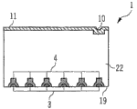
在图1a中所示出的壳体1的上侧2形成了发射辐射器件的辐射出射面。上侧2是第一层的正面,该第一层优选与设置在第一层之后的第二和第三层形成层堆叠,壳体1包含该层堆叠。The
第一层具有凹处6,该凹处从上侧2朝着第二层的方向逐渐变细。The first layer has a
在图1a中所示的壳体1中,在凹处6内设置有三个芯片区7。在每个芯片区7上可以设置一个辐射源,优选为发射辐射的半导体芯片。为了每个芯片的电连接,分别设置了引线接合区30和芯片区7。此外,设置了通孔3,其借助印制导线5与引线接合区30或者芯片区7相连。In the
优选的是,通孔3包含金属,特别优选的是包含钨。通孔3半圆形地构建。这些通孔沿着安装面19从上侧2朝着与上侧2对置的下侧延伸。通孔3可以如下形成:在三个不同的层中留出凹陷,这些凹陷例如借助电镀用钨覆盖或者填充。在此,金属层11可以用作电极。Preferably, the via 3 contains metal, particularly preferably tungsten. Through
在图1a中示出了六个通孔3,其中每两个相邻的通孔导电地与一个半导体芯片相连。此外,每两个相邻的通孔3分别形成了第一和第二电接触部。有利的是,每个半导体芯片可以分离地控制。替代地,半导体芯片可以串联或者并联。Six
在上侧2包围通孔3的金属化物4可以如金属化物10那样用于标记。借助通过金属化物4标识的通孔3的位置,在将壳体1安装到印刷电路板上时,可以使通孔3与设置在印刷电路板上的印制导线的电连接变得容易。同样,通过金属化物10可以更容易地确定壳体1的取向。The
此外,金属化物4可以有助于使得壳体1在红外或者回流焊接时自己聚集。Furthermore, the
水平线A-A形成了凹处6的中轴,并且与安装面19平行延伸。与距对置于安装面的侧面相比,该水平线距安装面19更远。凹处6的偏离中心的设置的优点是,使得所发射的辐射有效地耦合输入到例如光导体中。The horizontal line A-A forms the central axis of the
用虚线表示的附图组成部分是第二和第三层的元件,其将结合图3和4进一步阐述。Components of the drawings indicated by dashed lines are elements of the second and third layers, which will be explained further in conjunction with FIGS. 3 and 4 .
在图1b中示意性地示出了壳体1的横截面视图。可以看到层堆叠8,其包括三个层23、24、25,这些层包含陶瓷材料。A cross-sectional view of the
层23具有凹处6,该凹处有利地构建为反射器。对反射器的要求是,将设置在凹处6中的半导体芯片发射的辐射聚集,使得边发射器件具有特别高的辐射产量。这例如可以通过90°的张角9来实现。The
层24具有芯片凹陷26,该凹陷的大小与设置在芯片区7上的凹陷内的半导体芯片的大小匹配。The
层25例如可以用于冷却器件,并且由此有助于其稳定性。该层越厚,则可以吸收越多的热量。
为了以后将壳体1安装到例如印刷电路板上,要注意高度21与厚度20的比例。有利的是,该比例为2∶1。例如,高度可以为3.2mm,而厚度为1.65mm。For subsequent mounting of the
在图1c中示意性示出了与上侧2对置的下侧22。下侧22具有包围通孔3的金属化物4和金属化物10,这些金属化物用作壳体1定向的标记。下侧还具有用作电极的金属层11。The
在图2中示意性示出了不同视图中的壳体1的层23。The
层23特别是用于射束引导。为此,其具有凹处6。由设置在凹处6之下或者设置在凹处之内(参见图1a)的辐射源所产生的辐射通过该凹处从边发射器件中出射。射束引导可以有利地通过凹处6的形状来影响。
在图2a中示出了壳体1的上侧2,该上侧同时形成了边发射器件的辐射出射面。所示的是通孔3、金属化物4和10、电极11以及凹处6。凹处6可以如所示的那样椭圆形地成形。此外,该凹处可以从正面漏斗状地逐渐变细,直到层23的背面。FIG. 2 a shows the
在图2b中示意性示出了层23的横截面。层23包含陶瓷材料。在制造时,层23可以被部分地挖空,使得形成凹处6。凹处6在此等同于截顶锥体。该凹处适合于作为反射器,其中张角9优选为90°。同样,在图2c中以纵截面示出的凹处6的张角9也优选为90°。A cross-section of
在图2d中示出了层23的背面。金属化物4和10以及金属层11被施加在层23的正面和背面上,而通孔3从正面延伸直到背面,并且在此沿着安装面19走向。The backside of
在图3中示意性示出了不同的视图中的壳体1的层24。在图3a中示出了层24的正面。该正面在层堆叠中朝着层23的背面。层24在正面具有导电的引线接合区30。每个引线接合区30都与印制导线5相连,其中印制导线5与通孔3相邻。在至通孔3的边界上,印制导线5构造为使得通孔3精确地配合到印制导线5中。优选的是,通孔3在至印制导线5的边界上半圆形地构建,而印制导线5具有半圆形的凸状部。FIG. 3 schematically shows
通过印制导线5,可以建立至半导体芯片的电连接,其中芯片凹陷26是设置用于这些半导体芯片的。每个半导体芯片优选都借助线与设置用于相应的半导体芯片的引线接合区30相连。Electrical connections to the semiconductor chips for which chip recesses 26 are provided can be produced via the conductor tracks 5 . Each semiconductor chip is preferably connected by wire to a
印制导线5通过层23覆盖,而在凹处6中的引线接合区30暴露。The conductor tracks 5 are covered by the
芯片凹陷26被引入层24中。优选的是,其大小对应于芯片的大小。Chip recesses 26 are introduced into
在图3a中,在正面的与安装面19背离的侧上可以看到金属化物4的残余部分。这些残余部分是上面描述的将板非对称分离以制造单个器件的结果。In FIG. 3 a , a remnant of the
在图3b中示意性示出了层24的横截面。优选的是,芯片凹陷26从正面延伸直到层24的背面。特别优选的是,芯片凹陷26大致形成了方形的凹陷。A cross-section of
在图3c中示意性示出了层24的背面。其具有用作标志的金属化物4和10,此外还具有芯片凹陷26和通孔3。The rear side of
在图4中示意性示出了不同视图中的层25。The
在图4a中示意性示出了层25的正面。该正面朝着层24的背面,其中该背面几乎完全覆盖了该正面。只是芯片凹陷26形成了朝着层25的窗。通过这些窗,可以看见芯片区7。芯片可以设置在芯片区7上。印制导线5建立在芯片区7和通孔3之间的电连接。在此,层25的印制导线5所相邻的通孔3不同于层24的印制导线5所相邻的通孔3。The front side of
在图4a所示的实施例中,三个芯片可以设置在三个分离的芯片区7上,其中这些芯片可以被分离地控制。替代地,这些芯片可以并联或者串联,并且为此设置在共同的芯片区上。In the embodiment shown in Figure 4a, three chips can be arranged on three separate chip areas 7, wherein the chips can be controlled separately. Alternatively, the chips can be connected in parallel or in series and be arranged for this purpose on a common chip area.
在图4b中示意性示出了层25的横截面。层25可以形成散热装置。在此,优选包含在层25中的陶瓷材料证明是有利的。A cross-section of
在图4c中示意性示出了层25的背面,该背面同时形成了壳体1的背面22。FIG. 4 c schematically shows the rear side of
在图5中示出了板27,该板被分割为四个壳体1。优选的是,板27由陶瓷层堆叠形成。特别优选的是,层堆叠包括三层。这三层可以对应于图2至4中所示的层23、24、25构建。FIG. 5 shows a
由此,板27的第一层可以具有漏斗状的凹处6,其从形成壳体1的以后的上侧2的上侧延伸至第一层的背面。第一层之后设置有第二和第三层。从第二层可以看到引线接合区30,并且从第三层可以看到芯片区7。The first layer of the
优选的是,施加在板27上的金属化物4沿着直线12设置。板27可以沿着这些直线12被分离。有利的是,板27被分离为使得在侧面29上通孔3基本上被去除,而在安装面19上这些通孔被暴露。通过这种方式,壳体1仅仅在安装面19上获得电连接可能性。侧面29为了以后安装壳体1(例如安装到印刷电路板上)而被平滑,由此可以容易地装配。例如,板27可以沿着直线12锯开,其中锯痕有利地选择为对应于直线12的宽度。Preferably, the
进一步的分离可以沿着线28进行,其中板27在此例如可以借助折断来分离。A further separation can take place along the
在图6中以透视图示例性地示出了从板27切割出的边发射器件31。该器件具有层堆叠,其优选包括层23、层24和层25。层23设置有凹处6。在凹处6中在每个芯片区7上设置有芯片13,芯片借助导体14连接到引线接合区30。优选的是,芯片13用导电胶施加到芯片区7上。An edge-emitting component 31 cut out of a
半导体芯片13例如可以通过所发射的辐射的波长来区分。波长例如可以位于红色、绿色或者蓝色频谱范围中。The semiconductor chips 13 can be distinguished, for example, by the wavelength of the emitted radiation. The wavelength can lie, for example, in the red, green or blue spectral range.
在图7中示出了壳体1,该壳体安装在印刷电路板17上。当高度21与厚度20的比例选择为2∶1时,在安装时处理壳体1会变得容易。在焊接时,倾倒力15作用到壳体1上。这种力例如可以通过施加对称设置的焊脚(Lotkehlen)16来对抗。金属层18可以有利地满足在壳体1和印刷电路板17之间的导电和/或导热的连接功能。FIG. 7 shows the
要指出的是,层23、24和25可以由多个部分层组合而成。It is pointed out that the
自然,借助所描述的实施例对本发明的阐述并不能理解为本发明的限制。特别地,实施例的各个特征也可以以其它的方式组合。Naturally, the explanation of the invention with the aid of the described exemplary embodiments is not to be understood as limiting the invention. In particular, individual features of the exemplary embodiments can also be combined in other ways.
本专利申请要求德国专利申请102005024668.0的优先权,其公开内容通过引用结合于此。This patent application claims priority from German patent application 102005024668.0, the disclosure of which is hereby incorporated by reference.
Claims (26)
Applications Claiming Priority (2)
| Application Number | Priority Date | Filing Date | Title |
|---|---|---|---|
| DE102005024668.0 | 2005-05-30 | ||
| DE102005024668 | 2005-05-30 |
Publications (2)
| Publication Number | Publication Date |
|---|---|
| CN101213677A CN101213677A (en) | 2008-07-02 |
| CN100547821C true CN100547821C (en) | 2009-10-07 |
Family
ID=37057036
Family Applications (1)
| Application Number | Title | Priority Date | Filing Date |
|---|---|---|---|
| CNB2006800239603A Expired - Fee Related CN100547821C (en) | 2005-05-30 | 2006-05-05 | Housing and method for manufacturing the same |
Country Status (8)
| Country | Link |
|---|---|
| US (2) | US8288791B2 (en) |
| EP (1) | EP1886359B1 (en) |
| JP (1) | JP5279488B2 (en) |
| KR (1) | KR101267477B1 (en) |
| CN (1) | CN100547821C (en) |
| DE (1) | DE112006001414A5 (en) |
| TW (1) | TWI305949B (en) |
| WO (1) | WO2006128416A2 (en) |
Families Citing this family (17)
| Publication number | Priority date | Publication date | Assignee | Title |
|---|---|---|---|---|
| DE102008011254A1 (en) | 2007-09-19 | 2009-04-02 | Osram Opto Semiconductors Gmbh | Carrier element's recess closing method for semiconductor component i.e. LED, involves providing screen with openings, filling of recess of carrier element by screen through screen printing of viscous mass, and hardening viscous mass |
| DE102008049535A1 (en) * | 2008-09-29 | 2010-04-08 | Osram Opto Semiconductors Gmbh | LED module and manufacturing process |
| JP2011054736A (en) * | 2009-09-01 | 2011-03-17 | Sharp Corp | Light-emitting device, plane light source, and liquid crystal display device |
| US8431951B2 (en) * | 2009-10-01 | 2013-04-30 | Excelitas Canada, Inc. | Optoelectronic devices with laminate leadless carrier packaging in side-looker or top-looker device orientation |
| US9018074B2 (en) | 2009-10-01 | 2015-04-28 | Excelitas Canada, Inc. | Photonic semiconductor devices in LLC assembly with controlled molding boundary and method for forming same |
| US8791492B2 (en) | 2009-10-01 | 2014-07-29 | Excelitas Canada, Inc. | Semiconductor laser chip package with encapsulated recess molded on substrate and method for forming same |
| TWI407546B (en) * | 2010-02-24 | 2013-09-01 | 榮創能源科技股份有限公司 | Lateral light emitting semiconductor device package structure |
| JP2012032763A (en) * | 2010-06-28 | 2012-02-16 | Hitachi Consumer Electronics Co Ltd | Liquid crystal display device, backlight, and led |
| USD647865S1 (en) * | 2010-08-02 | 2011-11-01 | Citizen Electronics Co., Ltd. | Light-emitting diode |
| WO2012025888A2 (en) * | 2010-08-24 | 2012-03-01 | Colorchip (Israel) Ltd. | Light source mount |
| CN104112714B (en) * | 2013-04-19 | 2017-03-08 | 武汉赛丰科技有限公司 | Core shell, core casket and core system |
| KR20150004118A (en) * | 2013-07-02 | 2015-01-12 | 삼성디스플레이 주식회사 | Substrate for display device, method of manufacturing the same, and display device including the same |
| CN104681690A (en) * | 2013-12-03 | 2015-06-03 | 复盛精密工业股份有限公司 | Bracket structure of lateral light-emitting diodes |
| CN103873619B (en) * | 2014-03-23 | 2016-09-07 | 郑景文 | Sterilization mobile phone protective case |
| DE102014106791B4 (en) * | 2014-05-14 | 2023-01-19 | OSRAM Opto Semiconductors Gesellschaft mit beschränkter Haftung | Semiconductor device, lighting device and method for manufacturing a semiconductor device |
| US10098241B2 (en) * | 2015-10-23 | 2018-10-09 | International Business Machines Corporation | Printed circuit board with edge soldering for high-density packages and assemblies |
| JP6504019B2 (en) * | 2015-10-27 | 2019-04-24 | 豊田合成株式会社 | Light emitting device |
Citations (3)
| Publication number | Priority date | Publication date | Assignee | Title |
|---|---|---|---|---|
| US20040099942A1 (en) * | 2002-11-25 | 2004-05-27 | Samsung Electro-Mechanics Co., Ltd. | Ceramic multilayer substrate and method for manufacturing the same |
| US20040251044A1 (en) * | 2003-06-10 | 2004-12-16 | Choi Ik Seo | Ceramic package and fabrication method thereof |
| US20050093146A1 (en) * | 2003-10-30 | 2005-05-05 | Kensho Sakano | Support body for semiconductor element, method for manufacturing the same and semiconductor device |
Family Cites Families (32)
| Publication number | Priority date | Publication date | Assignee | Title |
|---|---|---|---|---|
| US4288841A (en) * | 1979-09-20 | 1981-09-08 | Bell Telephone Laboratories, Incorporated | Double cavity semiconductor chip carrier |
| US4328530A (en) * | 1980-06-30 | 1982-05-04 | International Business Machines Corporation | Multiple layer, ceramic carrier for high switching speed VLSI chips |
| US4681656A (en) * | 1983-02-22 | 1987-07-21 | Byrum James E | IC carrier system |
| US4852227A (en) * | 1988-11-25 | 1989-08-01 | Sprague Electric Company | Method for making a multilayer ceramic capacitor with buried electrodes and terminations at a castellated edge |
| DE58908841D1 (en) | 1989-05-31 | 1995-02-09 | Siemens Ag | Surface mount opto component. |
| US5223746A (en) | 1989-06-14 | 1993-06-29 | Hitachi, Ltd. | Packaging structure for a solid-state imaging device with selectively aluminium coated leads |
| JPH05275750A (en) | 1992-03-25 | 1993-10-22 | Sanyo Electric Co Ltd | Optical semiconductor device |
| EP0646971B1 (en) | 1993-09-30 | 1997-03-12 | Siemens Aktiengesellschaft | Two-terminal SMT-miniature-housing of semiconductor device and process of manufacturing the same |
| JP3472429B2 (en) | 1997-02-28 | 2003-12-02 | シャープ株式会社 | Method for manufacturing side-emitting display device |
| TW473882B (en) * | 1998-07-06 | 2002-01-21 | Hitachi Ltd | Semiconductor device |
| JP2001077408A (en) * | 1999-09-09 | 2001-03-23 | Rohm Co Ltd | Manufacturing method of infrared transceiver module and infrared transceiver module |
| US7078791B1 (en) * | 2001-05-09 | 2006-07-18 | Ess Technology, Inc. | Chip on board package for imager |
| JP3668438B2 (en) * | 2001-06-07 | 2005-07-06 | シャープ株式会社 | Chip light emitting diode |
| JP2003304002A (en) * | 2002-04-08 | 2003-10-24 | Sharp Corp | Method for manufacturing surface-mounted optical semiconductor device |
| SG107595A1 (en) * | 2002-06-18 | 2004-12-29 | Micron Technology Inc | Semiconductor devices and semiconductor device components with peripherally located, castellated contacts, assembles and packages including such semiconductor devices or packages and associated methods |
| WO2004001862A1 (en) * | 2002-06-19 | 2003-12-31 | Sanken Electric Co., Ltd. | Semiconductor light emitting device, method for producing the same and reflector for semiconductor light emitting device |
| JP2004253425A (en) | 2003-02-18 | 2004-09-09 | Tdk Corp | Multilayer capacitor |
| JP2004266124A (en) * | 2003-03-03 | 2004-09-24 | Matsushita Electric Ind Co Ltd | Semiconductor light emitting device |
| TWI249864B (en) * | 2003-03-20 | 2006-02-21 | Toyoda Gosei Kk | LED lamp |
| JP4166611B2 (en) * | 2003-04-01 | 2008-10-15 | シャープ株式会社 | Light emitting device package, light emitting device |
| CN102290409B (en) | 2003-04-01 | 2014-01-15 | 夏普株式会社 | Light-emitting apparatus |
| JP2005005380A (en) * | 2003-06-10 | 2005-01-06 | Sanyo Electric Co Ltd | Manufacturing method of semiconductor device |
| JP3876250B2 (en) * | 2003-06-24 | 2007-01-31 | スタンレー電気株式会社 | Surface mount semiconductor electronic component and manufacturing method |
| US20080025030A9 (en) * | 2003-09-23 | 2008-01-31 | Lee Kong W | Ceramic packaging for high brightness LED devices |
| US7288797B2 (en) * | 2004-01-20 | 2007-10-30 | Nichia Corporation | Semiconductor light emitting element |
| WO2005091383A1 (en) * | 2004-03-24 | 2005-09-29 | Renesas Yanai Semiconductor Inc. | Light-emitting device manufacturing method and light-emitting device |
| US7114252B2 (en) * | 2004-06-17 | 2006-10-03 | Toko, Inc. | Large scale simultaneous circuit encapsulating apparatus |
| KR100765945B1 (en) * | 2004-08-06 | 2007-10-10 | 가부시끼가이샤 아라이도 마테리아루 | Collective substrate, semiconductor element mounting member, semiconductor device, imaging device, light emitting diode constituting member, and light emitting diode |
| US7256483B2 (en) * | 2004-10-28 | 2007-08-14 | Philips Lumileds Lighting Company, Llc | Package-integrated thin film LED |
| TWI253714B (en) * | 2004-12-21 | 2006-04-21 | Phoenix Prec Technology Corp | Method for fabricating a multi-layer circuit board with fine pitch |
| JP4689637B2 (en) * | 2007-03-23 | 2011-05-25 | シャープ株式会社 | Semiconductor light emitting device |
| US7547630B2 (en) * | 2007-09-26 | 2009-06-16 | Texas Instruments Incorporated | Method for stacking semiconductor chips |
-
2006
- 2006-05-05 DE DE112006001414T patent/DE112006001414A5/en not_active Withdrawn
- 2006-05-05 KR KR1020077030545A patent/KR101267477B1/en not_active Expired - Fee Related
- 2006-05-05 WO PCT/DE2006/000778 patent/WO2006128416A2/en not_active Ceased
- 2006-05-05 CN CNB2006800239603A patent/CN100547821C/en not_active Expired - Fee Related
- 2006-05-05 JP JP2008513912A patent/JP5279488B2/en not_active Expired - Fee Related
- 2006-05-05 EP EP06722836.1A patent/EP1886359B1/en not_active Ceased
- 2006-05-05 US US11/921,368 patent/US8288791B2/en not_active Expired - Fee Related
- 2006-05-29 TW TW095119070A patent/TWI305949B/en not_active IP Right Cessation
-
2012
- 2012-09-12 US US13/611,890 patent/US8772065B2/en not_active Expired - Fee Related
Patent Citations (3)
| Publication number | Priority date | Publication date | Assignee | Title |
|---|---|---|---|---|
| US20040099942A1 (en) * | 2002-11-25 | 2004-05-27 | Samsung Electro-Mechanics Co., Ltd. | Ceramic multilayer substrate and method for manufacturing the same |
| US20040251044A1 (en) * | 2003-06-10 | 2004-12-16 | Choi Ik Seo | Ceramic package and fabrication method thereof |
| US20050093146A1 (en) * | 2003-10-30 | 2005-05-05 | Kensho Sakano | Support body for semiconductor element, method for manufacturing the same and semiconductor device |
Also Published As
| Publication number | Publication date |
|---|---|
| EP1886359B1 (en) | 2019-07-03 |
| DE112006001414A5 (en) | 2008-03-06 |
| EP1886359A2 (en) | 2008-02-13 |
| TW200703596A (en) | 2007-01-16 |
| KR20080016686A (en) | 2008-02-21 |
| WO2006128416A3 (en) | 2007-08-09 |
| WO2006128416A2 (en) | 2006-12-07 |
| KR101267477B1 (en) | 2013-05-31 |
| US8288791B2 (en) | 2012-10-16 |
| US20090230420A1 (en) | 2009-09-17 |
| JP2008546192A (en) | 2008-12-18 |
| TWI305949B (en) | 2009-02-01 |
| CN101213677A (en) | 2008-07-02 |
| US8772065B2 (en) | 2014-07-08 |
| JP5279488B2 (en) | 2013-09-04 |
| US20130005091A1 (en) | 2013-01-03 |
Similar Documents
| Publication | Publication Date | Title |
|---|---|---|
| CN100547821C (en) | Housing and method for manufacturing the same | |
| CN102893418B (en) | Lighting unit, lighting device | |
| US9595806B2 (en) | Laser light-emitting apparatus | |
| CN101471335B (en) | Method for manufacturing light emitting module | |
| EP2760058B1 (en) | Led module and led lamp employing same | |
| US7391153B2 (en) | Light emitting device provided with a submount assembly for improved thermal dissipation | |
| JP4432275B2 (en) | Light source device | |
| JP4122784B2 (en) | Light emitting device | |
| CN100391019C (en) | Semiconductor light emitting device and manufacturing method thereof | |
| CN103098247B (en) | Light-emitting device and method of manufacturing light-emitting device | |
| CN104798215B (en) | Optoelectronic semiconductor components with sapphire flip chips | |
| JP5302117B2 (en) | LIGHT EMITTING DEVICE MANUFACTURING METHOD, LIGHT EMITTING DEVICE, AND LIGHT EMITTING DEVICE MOUNTING BOARD | |
| CN101877382B (en) | Light emitting device package and lighting system including the same | |
| JP2003152225A (en) | Light emitting device | |
| US8901580B2 (en) | Package for mounting electronic components, electronic apparatus, and method for manufacturing the package | |
| TW200933927A (en) | Light emitting diode package | |
| WO2002089221A1 (en) | Light emitting device comprising led chip | |
| JP2007027433A (en) | Light emitting device | |
| CN103579129B (en) | Semiconductor component support and semiconductor device | |
| JP6348660B2 (en) | Optoelectronic semiconductor component and method for manufacturing optoelectronic semiconductor component | |
| JP2011249737A (en) | Lead frame, wiring board, and led unit using the same | |
| KR20130051485A (en) | Led module | |
| JP5347681B2 (en) | Light emitting device | |
| CN101476710A (en) | Illuminating device | |
| JP2023014090A (en) | Light source device |
Legal Events
| Date | Code | Title | Description |
|---|---|---|---|
| C06 | Publication | ||
| PB01 | Publication | ||
| C10 | Entry into substantive examination | ||
| SE01 | Entry into force of request for substantive examination | ||
| C14 | Grant of patent or utility model | ||
| GR01 | Patent grant | ||
| CF01 | Termination of patent right due to non-payment of annual fee | ||
| CF01 | Termination of patent right due to non-payment of annual fee |
Granted publication date: 20091007 |