CN100539000C - Capacitive coupling plasma processing apparatus - Google Patents
Capacitive coupling plasma processing apparatus Download PDFInfo
- Publication number
- CN100539000C CN100539000C CNB2005101275549A CN200510127554A CN100539000C CN 100539000 C CN100539000 C CN 100539000C CN B2005101275549 A CNB2005101275549 A CN B2005101275549A CN 200510127554 A CN200510127554 A CN 200510127554A CN 100539000 C CN100539000 C CN 100539000C
- Authority
- CN
- China
- Prior art keywords
- plasma
- processing apparatus
- plasma processing
- chamber
- electrode
- Prior art date
- Legal status (The legal status is an assumption and is not a legal conclusion. Google has not performed a legal analysis and makes no representation as to the accuracy of the status listed.)
- Expired - Fee Related
Links
Images


Landscapes
- Plasma Technology (AREA)
- Drying Of Semiconductors (AREA)
Abstract
本发明提供一种电容耦合型的等离子体处理装置(100),包括可设定为具有真空气氛的处理腔室和将处理气体供给腔室(1)内的处理气体供给部(15)。在腔室(1)内、第一电极(2)和第二电极(18)相对地配置。为了在第一和第二电极间的等离子体生成区域(R1)中形成高频电场,配置将高频电力供给至第一或第二电极的高频电源(10)。高频电场使处理气体变成等离子体。被处理基板(W)在第一和第二电极之间,由支撑部件(2)所支撑,使其被处理面与第二电极(18)相对。在等离子体生成区域(R1)周围的周围区域(R2)中,配置接地的导电性作用面AS,以扩展等离子体,进行调制,使得与等离子体实质上直流地结合。

The present invention provides a capacitively coupled plasma processing apparatus (100), comprising a processing chamber which can be set to have a vacuum atmosphere, and a processing gas supply part (15) for supplying processing gas into the chamber (1). In the chamber (1), the first electrode (2) and the second electrode (18) are arranged facing each other. In order to form a high-frequency electric field in a plasma generation region (R1) between the first and second electrodes, a high-frequency power supply (10) for supplying high-frequency power to the first or second electrodes is arranged. The high-frequency electric field turns the process gas into a plasma. The substrate to be processed (W) is supported by a support member (2) between the first and second electrodes so that the surface to be processed is opposed to the second electrode (18). In a peripheral region (R2) around the plasma generation region (R1), a grounded conductive active surface AS is arranged to spread the plasma, modulated so as to combine substantially direct current with the plasma.
Description
技术领域 technical field
本发明例如涉及在半导体处理系统中,用于对被处理基板进行等离子体处理而使用的电容耦合型等离子体处理装置。这里,所谓半导体处理表示的是通过在半导体晶片或LCD(液晶显示器)或FPD(平板显示器)用的玻璃基板等的被处理基板上,通过以给定的图形而形成半导体层、绝缘层、导电层等,而为了在该被处理基板上制造包含半导体设备和与半导体设备连接的线路、电极等的结构物所进行的各种处理。The present invention relates to, for example, a capacitively coupled plasma processing apparatus used for plasma processing a substrate to be processed in a semiconductor processing system. Here, the term "semiconductor processing" refers to forming semiconductor layers, insulating layers, conductive layers, etc. Layers, etc., and various processes for manufacturing structures including semiconductor devices and wiring, electrodes, etc. connected to the semiconductor devices on the substrate to be processed.
背景技术 Background technique
例如,在半导体设备的制造过程中,多数采用对作为被处理基板的半导体晶片进行蚀刻或溅射、CVD(化学气相沉积)等的等离子体处理。作为用于进行这种等离子体处理的等离子体处理装置,使用各种装置,其中,以电容耦合型平行平板等离子体处理装置为主流。For example, in the manufacturing process of semiconductor devices, plasma processing such as etching or sputtering, CVD (Chemical Vapor Deposition), and the like is often used on a semiconductor wafer as a substrate to be processed. As a plasma processing apparatus for performing such plasma processing, various apparatuses are used, and among them, a capacitively coupled parallel plate plasma processing apparatus is the mainstream.
一般,电容耦合型的平行平板等离子体处理装置具有配置在处理腔室内的一对平行板电极(上部和下部电极)。处理时,将处理气体导入到腔室内,同时,将高频电力供给一个电极,在电极间形成高频电场而产生高频放电。利用这种高频放电来形成处理气体的等离子体,对半导体晶片的给定的层,例如进行等离子体蚀刻。Generally, a capacitively coupled parallel-plate plasma processing apparatus has a pair of parallel-plate electrodes (upper and lower electrodes) arranged in a processing chamber. During processing, a processing gas is introduced into the chamber, and at the same time, high-frequency power is supplied to one electrode, and a high-frequency electric field is formed between the electrodes to generate a high-frequency discharge. Such a high-frequency discharge is used to form a plasma of a process gas to perform plasma etching on a given layer of a semiconductor wafer, for example.
作为这种装置,例如有向放置半导体晶片的下部电极供给高频电力的形式。在这种情况下,下部电极起阴极作用,上部电极起阳极作用。另外,施加在下部电极上的高频电力兼有等离子体生成和对被处理基板施加高频偏压的作用。As such a device, for example, there is a form in which high-frequency power is supplied to a lower electrode on which a semiconductor wafer is placed. In this case, the lower electrode acts as a cathode and the upper electrode acts as an anode. In addition, the high-frequency power applied to the lower electrode serves both to generate plasma and to apply a high-frequency bias to the substrate to be processed.
在这种电容耦合型的平行平板等离子体处理装置中,存在于等离子体生成区域中的部件必需防止金属污染和消耗。由于这样,作为这些部件,使用形成有Y2O3等的耐等离子体性高的绝缘性陶瓷的涂层等的部件或石英制的部件。In such a capacitive coupling type parallel plate plasma processing apparatus, components present in the plasma generation region must be prevented from metal contamination and consumption. Therefore, as these members, those coated with insulating ceramics having high plasma resistance such as Y 2 O 3 , or those made of quartz are used.
然而,近年来,在半导体等制造过程中的设计规则日益微细,特别是在等离子体蚀刻中,要求更高的尺寸精度,要求进一步提高蚀刻的掩模和衬底的选择比和面内均匀性。由于这样,趋向降低的腔室内的处理区域的压力、降低离子能量。因此,使用40MHz以上的,比现有技术特别高的频率的高频。However, in recent years, the design rules in the manufacturing process of semiconductors have become increasingly finer, especially in plasma etching, higher dimensional accuracy is required, and the selection ratio and in-plane uniformity of the etching mask and substrate are required to be further improved. . Due to this, there tends to be a reduced pressure in the processing region within the chamber, reducing ion energy. Therefore, a high frequency of 40 MHz or higher is used, which is an extremely higher frequency than the conventional technology.
然而,通过降低压力和降低离子能量,而使等离子体的电阻率提高,控制等离子体的均匀性变得困难。具体地是,当施加在高频施加电极上的高频的频率高时,从高频电源供给电极背面的高频,由于表皮效果而在电极表面传送,集中在电极主面(与等离子体相对的面)的中心部。由于这样,电极主面的中心部分的电场强度比外周部的电场强度高,生成的等离子密度在电极中心部也比电极外周部高。在等离子体密度高的电极中心部,等离子体的电阻率低,在相对的电极中电流也集中在电极中心部。因此,等离子体密度不均匀而更强,引起蚀刻等的等离子体处理的面内不均匀和充电(charge up)损坏。However, by lowering the pressure and lowering the ion energy, the resistivity of the plasma increases, making it difficult to control the uniformity of the plasma. Specifically, when the frequency of the high frequency applied to the high frequency application electrode is high, the high frequency supplied from the high frequency power supply to the back of the electrode is transmitted on the surface of the electrode due to the skin effect, and is concentrated on the main surface of the electrode (opposite to the plasma). the center of the face). Because of this, the electric field intensity in the central portion of the main surface of the electrode is higher than that in the outer peripheral portion, and the generated plasma density is also higher in the electrode central portion than in the electrode outer peripheral portion. At the center of the electrode where the plasma density is high, the resistivity of the plasma is low, and the current also concentrates at the center of the electrode in the opposite electrode. Therefore, the plasma density becomes non-uniform and stronger, causing in-plane non-uniformity and charge-up damage in plasma processing such as etching.
为了解决这个问题,已知利用高电阻部件构成高频施加电极的主面中心部(专利文献1:日本专利特开2000-323456号)。采用这种技术,利用高电阻部件构成高频施加电极的主面中心部,这样,更多的高频电力作为焦耳热而被消耗。这样,在电极中心部,相对地使高频施加电极的主面的电场强度在电极中心部比在电极外周部低,可以校正上述的等离子体密度的不均匀性。然而,在用高电阻部件构成高频施加电极的主面中心部时,由焦耳热而引起的高频电力的消耗(能量损失)多,效率不好。In order to solve this problem, it is known to form the central part of the main surface of the high-frequency application electrode with a high-resistance member (Patent Document 1: Japanese Patent Laid-Open No. 2000-323456). With this technique, a high-resistance member is used to form the central portion of the main surface of the high-frequency application electrode, so that more high-frequency power is consumed as Joule heat. In this way, the electric field intensity of the main surface of the high-frequency application electrode is relatively lower in the center of the electrode than in the outer periphery of the electrode, so that the above-mentioned unevenness in plasma density can be corrected. However, when the central portion of the main surface of the high-frequency application electrode is formed of a high-resistance member, high-frequency power consumption (energy loss) due to Joule heat is large, and the efficiency is not good.
发明内容 Contents of the invention
本发明的目的在于提供一种等离子体处理的面内均匀性高,并且难以产生充电损坏的电容耦合型等离子体处理装置。An object of the present invention is to provide a capacitively coupled plasma processing apparatus that has high in-plane uniformity in plasma processing and is less prone to charge damage.
本发明的第一方面的电容耦合型的等离子体处理装置,包括:The capacitively coupled plasma processing apparatus of the first aspect of the present invention includes:
能够设定为具有真空气氛的处理腔室;Can be set as a processing chamber with a vacuum atmosphere;
将处理气体供给上述腔室内的处理气体供给部;supplying a processing gas to a processing gas supply unit in the chamber;
配置在上述腔室内的第一电极;a first electrode disposed in the chamber;
与上述第一电极相对而配置在上述腔室内的第二电极;a second electrode disposed in the chamber opposite to the first electrode;
为了在上述第一和第二电极之间的等离子体生成区域中形成高频电场,将高频电力供给上述第一或者第二电极的高频电源;利用上述高频电场来使上述处理气体等离子体化(变成等离子体);In order to form a high-frequency electric field in the plasma generation region between the above-mentioned first and second electrodes, high-frequency power is supplied to the high-frequency power supply of the first or second electrode; Integrate (turn into plasma);
在上述第一和第二电极之间支撑被处理基板、使其被处理面与上述第二电极相对的支撑部件;a support member that supports the substrate to be processed between the first and second electrodes so that the surface to be processed is opposed to the second electrode;
在上述腔室内配置在上述等离子体生成区域周围的周围区域中、并且接地的导电性的作用面,可使上述等离子体向上述等离子体生成区域的外侧扩展,以及可调制上述作用面,使其实质上与上述等离子体直流地结合。A conductive active surface arranged in the surrounding area around the plasma generation region and grounded in the chamber can spread the plasma to the outside of the plasma generation region, and can modulate the active surface so that Combined substantially direct current with the aforementioned plasma.
采用第一方面的装置,当在腔室内生成等离子体时,电流从等离子体流向设置在被处理基板周围的作用面。其结果,等离子体向外侧扩展,使等离子体密度均匀化,这样,可提高等离子体处理的面内均匀性,同时可减少充电损坏。With the apparatus of the first aspect, when plasma is generated in the chamber, current flows from the plasma to the active surface provided around the substrate to be processed. As a result, the plasma spreads outward and the plasma density is made uniform, thereby improving the in-plane uniformity of the plasma treatment and reducing charging damage.
附图说明 Description of drawings
图1是表示作为本发明的第一实施方式的等离子体处理装置的等离子体蚀刻装置的截面图。1 is a cross-sectional view showing a plasma etching apparatus as a plasma processing apparatus according to a first embodiment of the present invention.
图2是表示使等离子体生成用的高频电源和离子导入用的高频电源与作为下部电极的支撑台连接的状态的简要截面图。2 is a schematic cross-sectional view showing a state in which a high-frequency power source for plasma generation and a high-frequency power source for ion introduction are connected to a support as a lower electrode.
图3是表示现有技术的等离子体蚀刻装置的简要结构的示意图。FIG. 3 is a schematic diagram showing a schematic configuration of a conventional plasma etching apparatus.
图4是用于说明通过图1所示的等离子体蚀刻装置来使等离子体密度均匀化的原理的示意图。FIG. 4 is a schematic diagram for explaining the principle of uniformizing plasma density by the plasma etching apparatus shown in FIG. 1 .
图5是表示第一实施方式的等离子体蚀刻装置的变形例的示意图。FIG. 5 is a schematic diagram showing a modified example of the plasma etching apparatus of the first embodiment.
图6是表示第一实施方式的等离子体蚀刻装置的另一个变形例的示意图。FIG. 6 is a schematic diagram showing another modified example of the plasma etching apparatus of the first embodiment.
图7是表示第一实施方式的等离子体蚀刻装置的又一个变形例的示意图。FIG. 7 is a schematic diagram showing still another modified example of the plasma etching apparatus of the first embodiment.
图8是表示通过比较屏蔽部件的高度不同的第一实施方式的实施例和现有技术的比较例而得到的晶片的面内位置的Vdc值的图形。FIG. 8 is a graph showing Vdc values at in-plane positions of the wafer obtained by comparing examples of the first embodiment in which shield members have different heights and comparative examples of the prior art.
图9是表示通过比较图8所示的实施例和比较例而得到的ΔVdc的功率的依存性的图。FIG. 9 is a graph showing the power dependence of ΔVdc obtained by comparing the example shown in FIG. 8 with the comparative example.
图10是表示通过排气环的位置不同的第一实施方式的实施例而得出的晶片的面内位置的Vdc值的图。FIG. 10 is a graph showing Vdc values at in-plane positions of the wafer obtained in Examples of the first embodiment in which the position of the exhaust ring is different.
图11是表示通过图10所述的实施而得出到ΔVdc的功率的依存性的图。FIG. 11 is a graph showing the power dependence of ΔVdc obtained by the implementation described in FIG. 10 .
图12是表示作为本发明的第二实施方式的等离子体处理装置的等离子体蚀刻装置的截面图。12 is a cross-sectional view showing a plasma etching apparatus as a plasma processing apparatus according to a second embodiment of the present invention.
图13是说明通过图12所示的等离子体蚀刻装置而使等离子体密度均匀化的原理的示意图。FIG. 13 is a schematic diagram illustrating the principle of uniformizing plasma density by the plasma etching apparatus shown in FIG. 12 .
图14是表示第二实施方式的等离子体蚀刻装置的变形例的示意图。FIG. 14 is a schematic diagram showing a modified example of the plasma etching apparatus of the second embodiment.
图15是表示第二实施方式的等离子体蚀刻装置的另一个变形例的示意图。FIG. 15 is a schematic diagram showing another modified example of the plasma etching apparatus of the second embodiment.
图16为表示在图14和图15所示的等离子体蚀刻装置中所使用的接地部件的变形例的示意图。FIG. 16 is a schematic view showing a modified example of the ground member used in the plasma etching apparatus shown in FIGS. 14 and 15 .
图17是表示在图14和图15所示的等离子体蚀刻装置中所使用的接地部件的另一个变形例的示意图。FIG. 17 is a schematic view showing another modified example of the ground member used in the plasma etching apparatus shown in FIGS. 14 and 15 .
图18是表示图17所示的接地部件和处理腔室的关系的横截平面图。18 is a cross-sectional plan view showing the relationship between the ground member shown in FIG. 17 and the processing chamber.
具体实施方式 Detailed ways
以下,参照附图,对本发明的实施方式进行说明。其中,在以下的说明中,对具有大致相同的功能和结构的元件,标注相同的标号,并只在必要的情况下进行重复的说明。Hereinafter, embodiments of the present invention will be described with reference to the drawings. However, in the following description, elements having substantially the same function and structure are denoted by the same reference numerals, and description will be repeated only when necessary.
(第一实施方式)(first embodiment)
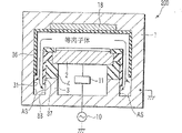
图1是表示作为本发明的第一实施方式的等离子体处理装置的等离子体蚀刻装置的截面图。该装置构成为可蚀刻配置在半导体晶片上的氧化膜(SiO2膜)。1 is a cross-sectional view showing a plasma etching apparatus as a plasma processing apparatus according to a first embodiment of the present invention. This device is configured to etch an oxide film (SiO 2 film) disposed on a semiconductor wafer.
该等离子体蚀刻装置100具有气密性构成的、大致呈圆筒形的处理腔室1。该腔室1的主体例如由铝等金属制成,在其内壁表面上形成有氧化处理薄膜或者由Y2O3等绝缘陶瓷制成的薄膜(例如喷镀薄膜)这种绝缘膜。腔室1接地。The
在该腔室1内配置有水平支撑作为被处理基板的晶片W的、并作为下部电极而作用的支撑台2。支撑台2例如由表面经过氧化处理的铝所构成。环状的支撑部3从腔室1的底壁突出,与支撑台2的外周对应。在该支撑部3上配置环状的绝缘部件4,支撑台2的外边缘部通过该绝缘部件4而被支撑。A support table 2 that horizontally supports a wafer W as a substrate to be processed and functions as a lower electrode is arranged in the
在绝缘部件4的外侧,在支撑部3上形成环状的导电性屏蔽部件25。其上端的高度位置在晶片W的上表面附近。该屏蔽部件25通过腔室1或者通过以下所示的排气环14和腔室1而直流地接地。在支撑台2的上方的外周上配置有由导电性材料(例如Si、SiC)等制成的聚焦环5。在屏蔽部件25的下端和腔室1的周壁之间配置有圆锥形的排气环14。对于排气环14来说,在使处理气体通过而导入排气管线的同时,如后所述,还起到规定等离子体生成区域周围的周围区域的作用。在该排气环14的表面上形成由Y2O3等的绝缘陶瓷构成的绝缘膜。此外,在支撑台2和腔室1的底壁之间形成有空洞部7。On the outer side of the insulating
在支撑台2的表面部分上配置有用于静电吸着晶片W的静电卡盘6。该静电卡盘6在绝缘体6b之间放置电极6a而构成,直流电源13通过开关13a而与电极6a连接。而且,通过将电压从直流电源13施加在电极6a上,而利用静电力(例如库仑力)来吸附半导体晶片W。An electrostatic chuck 6 for electrostatically holding wafer W is disposed on a surface portion of support table 2 . This electrostatic chuck 6 is configured by placing an
在支撑台2内设置有制冷剂流路8a,制冷剂管路8b与该制冷剂流路8a连接。通过制冷剂控制装置8,将适当的制冷剂经由该制冷剂管路8b而供给到制冷剂流路8a并循环。这样,可将支撑台2控制在适当温度。此外,在静电卡盘6的表面和晶片W的背面之间配置有用于供给传热用的传热气体(例如He气体)的传热气体管路9a。从传热气体供给装置9经由传热气体管路9a而将传热气体供给至晶片W的背面。这样,即使腔室1内排气而保持真空,在制冷剂流路8a中循环的制冷剂的冷热也可以高效率地传递给晶片W,可提高晶片W的温度控制性。A
供给高频电力用的给电线12与支撑台2的大致中心连接。匹配器11和高频电源10与该给电线12连接。从高频电原10将规定频率的高频电力供给至支撑台2。A
另一方面,与支撑台2相对,在其上方配置也作为上部电极的喷淋头18(以下称为上部电极18)。喷淋头18嵌入腔室1的顶壁部分中。该喷淋头18具有导电性的主体18a,多个气体输出孔18d形成为贯通主体18a的下部。气体输出孔18d与在主体18a的内部形成的空间18c和在上部形成的气体导入部18b连通。气体导入部18b通过气体供给管路15a而与供给蚀刻用的处理气体的处理气体供给装置15连接。On the other hand, a shower head 18 (hereinafter referred to as an upper electrode 18 ) also serving as an upper electrode is arranged on the opposite side of the support table 2 . The
上部电极18通过腔室1接地,与供给高频电力并作为下部电极而起作用的支撑台2一起,构成一对平行平板电极。作为供给高频电力的下部电极的支撑台2起到阴极作用,接地的上部电极18起到阳极作用。在上部电极18和支撑台2之间形成使处理气体成为等离子体的等离子体生成区域R1。此外,至等离子体生成区域R1周围的排气环14的区域成为周围区域R2。The
上部电极18的主体18a由金属或半导体(例如碳或者Si)等构成。为了防止金属污染或等离子体造成的消耗,特别是发生损伤,主体18a的与支撑台2相对的对向面通过绝缘膜而覆盖(参照后述的绝缘膜27)。该绝缘膜由氧化处理薄膜或者Y2O3等绝缘陶瓷制成的薄膜(例如喷镀薄膜)等而形成。The
作为蚀刻用的处理气体,可以采用现有技术中使用的各种气体,例如可以使用含有碳氟化合物气体(CxFy)或者含氢碳氟化合物(CpHqFr)的卤素元素的气体。此外,也可以再添加Ar、He等稀有气体或者N2气体、O2气体等。另外,在灰化中使用的情况下,作为处理气体可以使用O2气体等。As the processing gas for etching, various gases used in the prior art can be used, for example, halogen elements containing fluorocarbon gas (C x F y ) or hydrogen-containing fluorocarbon (C p H q F r ) can be used. gas. In addition, rare gases such as Ar and He, N 2 gas, O 2 gas, and the like may be further added. In addition, when used for ashing, O 2 gas or the like can be used as a processing gas.
这种处理气体从处理气体供给装置15,经由气体供给管路15a、气体导入部18b,而通至主体18a内的空间18c。处理气体从气体输出孔18d输出,供蚀刻在晶片W上形成的膜用。Such processing gas is passed from the processing
排气管19与腔室1的底壁连接。包含真空泵等的排气装置20与该排气管19连接。而且,通过使排气装置20的真空泵工作,可将腔室1内减压至规定的真空度。另一方面,在腔室1的侧壁的上侧,配置有开闭晶片W的搬入搬出口23的闸阀24。The
另一方面,在腔室1的搬入搬出口23的上下,以围绕腔室1的方式而配置有两个圆环磁铁21a、21b。利用圆环磁铁21a、21b,在支撑台2和上部电极18之间的处理空间的周围形成磁场。该圆环磁铁21a、21b通过图中没有示出的旋转机构而能够转动。On the other hand, two
圆环磁铁21a、21b,由永久磁铁构成的多个扇形体磁铁而在多极状态下配置成圆环形。即,在圆环磁铁21a、21b中,相邻的多个扇形磁铁彼此的磁极方向配置成互相相反。因此,磁力线在相邻的扇形体磁铁之间形成,只在处理空间的周边形成0.02~0.2T(200~2000高斯)、优选为0.03~0.045T(300~450高斯)的磁场。晶片配置部分实质上成为无磁场状态。这样,可得到适当的等离子体限制效应的效果。所谓晶片配置部分的实质上无磁场状态并不是只限于完全不存在磁场的情况。例如,这个概念也包含在晶片配置部分形成磁场,但该磁场对等离子体处理实质上没有影响的情况。The
如上所述,导电性屏蔽部件25通过腔室1或者通过排气环14和腔室1而直流地接地。配置在周围区域R2上的屏蔽部件25的表面,可起到将等离子体在等离子体生成区域R1的外侧扩展用的导电性作用面AS的作用。可以调制该作用面AS,使其直流地与等离子体结合而且相对于支撑台2上的晶片W同心状地配置。具体地是,屏蔽部件25例如由无垢的铝、表面经阳极氧化的铝、Si(掺杂有杂质,使得具有导电性)、SiC、C(碳)、W等具有导电性的材料构成。例如,在使用表面经过阳极氧化的铝的情况下,作用面AS可以由作为绝缘体的Al2O3膜所覆盖。但是,由于该绝缘膜十分薄,因此作用面AS可以直流地与等离子体结合。As mentioned above, the conductive shielding
另一方面,腔室1、上部电极18和排气环14接地,腔室1的内壁、上部电极18的对向面、排气环14的表面由Y2O3的绝缘膜(比屏蔽部件25的表面绝缘膜厚)覆盖。由于这样,这些部件的表面与等离子体交流地或高频地结合。另外,聚焦环5通过支撑台2与高频电源10连接。因此,区分等离子体生成电区域R1和周围区域R2的构成元件表面不包含除了屏蔽部件25的表面(作用面AS)与等离子体直流结合而被调制的面。On the other hand, the
为了调整等离子体密度和离子导入作用,也可以使等离子体生成用的高频电力和将等离子体中的离子导入用的高频电力重叠。具体地是,如图2所示,除了与匹配器11连接的等离子体生成用高频电源10以外,将离子导入用的高频电源26与匹配器11b连接,使其重叠。在这种情况下,作为离子导入用的高频电源26的频率优选为500KHz~27MHz。这样,可以控制离子能量而进一步提高蚀刻速度等的等离子体处理速度。In order to adjust the plasma density and the ion introduction action, the high-frequency power for generating plasma and the high-frequency power for introducing ions in the plasma may be superimposed. Specifically, as shown in FIG. 2 , in addition to the high-
等离子体蚀刻装置100的各个构成部,与控制部(过程控制器)50连接来进行控制。具体地是,通过控制部50来控制制冷剂控制装置8、传热气体供给装置9、排气装置20、静电卡盘6用的直流电源13的开关13a、高频电源10、和匹配器11等。Each constituent unit of the
此外,由用于工程管理者管理等离子体蚀刻装置100而进行指令输入的操作等的键盘、和可视化显示等离子体处理装置100的工作状况的显示器等所构成的用户界面51,与控制部50连接。In addition, a
而且,存放有通过控制部50的控制而实现由等离子体蚀刻装置100进行的各种处理的控制程序、和根据处理条件而在等离子体蚀刻装置的各个构成部上进行处理用的程序(即方法)的存储部52,与控制部50连接。方法也可以存储在硬盘或者半导体存储器中,在收容于CDROM、DVD等可搬性的存储介质中的状态下,也可以安装在存储部52的规定位置上。In addition, a control program for realizing various processes performed by the
而且,根据需要,通过从存储部52中调出由用户界面51发出的指示等中的任意方法并在控制部50中实行,而在控制部50的控制下,进行由等离子体蚀刻装置100进行的希望的处理。Furthermore, by calling any method such as an instruction from the
其次,说明这样构成的等离子体蚀刻装置的处理动作。Next, the processing operation of the plasma etching apparatus configured in this way will be described.
首先,打开图1的等离子体蚀刻装置100的闸阀24,利用搬送臂而将具有有蚀刻对象层的晶片W搬入腔室1内,并放置在支撑台2上。接着,使搬送臂退避而关闭闸阀24,通过排气装置20的真空泵并经由排气管19而将腔室1内抽成规定的真空度。First, the
然后,将蚀刻用的处理气体以规定的流量从处理气体供给装置15导入到腔室1内,将腔室1内维持在规定的压力,例如0.13~133.3Pa(1~1000mTorr)。这样,在保持规定压力的状态下,从高频电源10将频率为40MHz以上(例如100MHz)的高频电力供给至支撑台2。这时,从直流电源13将规定的电压施加在静电卡盘6的电极6a上,利用库仑力来吸附晶片W。Then, a processing gas for etching is introduced into the
这样,通过将高频电力施加在作为下部电极的支撑台2上,而在作为上部电极的喷淋头18和作为下部电极的支撑台2之间的处理空间(等离子体生成区域)中形成高频电场。这样,供给到处理空间中的处理气体成为等离子体,利用该等离子体来蚀刻在晶片W上形成的蚀刻对象层。In this way, by applying high-frequency power to the support table 2 as the lower electrode, a high-voltage plasma is formed in the processing space (plasma generation region) between the
在该蚀刻时,通过多极状态的圆环磁铁21a、21b而在处理空间周围形成磁场。这样,发挥适当的等离子体限制效应效果,可辅助等离子体的均匀化。此外,也有利用膜而没有这种磁场的效果的时候,在这种情况下,也可以使扇形体磁铁旋转而在处理空间周围实质上不形成磁场来进行处理。During this etching, a magnetic field is formed around the processing space by the
当形成上述磁场时,通过设置在支撑台2上的晶片W的周围的导电性聚焦环5而直到聚焦环区域为止起到下部电极的作用。由于这样,等离子体形成区域扩展至聚焦环5上,可促进晶片W周边部分的等离子体处理,可提高蚀刻速度的均匀性。When the above-mentioned magnetic field is formed, the
此外,配置在等离子体生成区域R1周围的周围区域R2上的屏蔽部件25可提供以下所述的效果。In addition, the shielding
图3是表示现有技术的等离子体蚀刻装置的简要结构的示意图。在现有技术的等离子体蚀刻装置中,在支撑台2的周围,配置有在表面上形成Y2O3等的绝缘膜27的屏蔽部件25’。由于该绝缘膜27厚,所以屏蔽部件25’的表面不能与等离子体直流地结合。而且,在屏蔽部件25’的内侧,配置有在屏蔽部件25’的上部外伸的绝缘部件4’。另外,在腔室1内,接地的其他部件(例如腔室1、上部电极18和排气环14)全部由Y2O3喷镀薄膜等的绝缘膜27和绝缘部件4’所覆盖。由于这样,这些部件的表面与等离子体不是直流地、而是交流地(高频地)结合。因此,这些部件只构成高频电流的图形回路,对校正等离子体的不均匀性没有作用。FIG. 3 is a schematic diagram showing a schematic configuration of a conventional plasma etching apparatus. In the conventional plasma etching apparatus, a shield member 25' having an insulating
图4是用于说明利用图1所示的等离子体蚀刻装置使等离子体密度均匀的原理的示意图。如上所述,导电性屏蔽部件25直流地接地,其表面起实质上与等离子体直流地结合的作用面AS的作用。如图4所示,当生成等离子体时,电流通过设置在晶片W的周围的作用面AS而从等离子体流向屏蔽部件25。其结果,等离子体向外侧扩展,从而,使等离子体密度均匀化。这样,可以在提高蚀刻处理的面内均匀性的同时,减少控制极氧化膜的绝缘破坏等的充电损坏。FIG. 4 is a schematic diagram for explaining the principle of making plasma density uniform by the plasma etching apparatus shown in FIG. 1 . As described above, the conductive shielding
其中,多极圆环磁铁21a、21b可发挥等离子体的限制效应来防止等离子体生成区域R1的周边边缘部的等离子体扩散。即,多极圆环磁铁21a、21b具有与带有使中央部的等离子体扩展的效果的屏蔽部件25相反的功能。因此,在利用多极圆环磁铁21a、21b形成磁场时,必需设定条件,使得不妨碍屏蔽部件25的扩展等离子体的效果。Among them, the
如上所述,为了发挥扩展等离子体来使等离子体密度均匀化的效果,可使屏蔽部件25的作用面AS的上端的高度位置比晶片W的高度位置高。在这种情况下,可使电流更容易从等离子体流向屏蔽部件25。As described above, the height position of the upper end of the action surface AS of the
图5是表示第一实施方式的等离子体蚀刻装置的变形例的示意图。在图1的结构中,屏蔽部件25的上端面和面向排气路的侧面的全部起到与等离子体直流地结合的作用面AS的作用。与此相对,在图5的变形例中,屏蔽部件25的下部通过厚的绝缘膜27所覆盖。即,只有屏蔽部件25的上部25a的表面起到与等离子体直流结合的作用面AS的作用。在这样的结构中,可以发挥使上述等离子体向外侧扩展而均匀化的功能。FIG. 5 is a schematic diagram showing a modified example of the plasma etching apparatus of the first embodiment. In the structure of FIG. 1 , all of the upper end surface and the side surface facing the exhaust path of the shielding
图6是表示第一实施方式的等离子体蚀刻装置的另一变形例的示意图。在图6的变形例中,使用表面不被绝缘膜所覆盖的排气环14a。除了屏蔽部件25以外,排气环14a的上表面也起到与等离子体直流地结合的作用面AS的作用。这样,电流可从等离子体向着屏蔽部件25和排气环14a而流向晶片W的外面,同样,可以使等离子体向外侧扩展而发挥均匀化的作用。在这种情况下,当用厚的绝缘膜覆盖屏蔽部件25时,可以只使排气环14的上表面起与等离子体直流地结合的作用面AS的作用。FIG. 6 is a schematic diagram showing another modified example of the plasma etching apparatus of the first embodiment. In the modified example of FIG. 6, the
图7是表示第一实施方式的等离子体蚀刻装置的又一个变形例的示意图。在图7的变形例中,排气环14’被配置在比配置图1的排气环14的位置下方的腔室1的底部附近。因此,等离子体生成区域周围的周围区域向下方扩展。此外,可使该排气环14’和屏蔽部件25的表面起到与等离子体直流地结合的作用面AS的作用。这样,等离子体向外侧扩展的效果提高,可以进一步提高使等离子体均匀化的功能。当利用厚的绝缘膜覆盖屏蔽部件25时,可以只使排气环14’的上表面起到与等离子体直流地结合的作用面AS的作用。FIG. 7 is a schematic diagram showing still another modified example of the plasma etching apparatus of the first embodiment. In the modified example of FIG. 7 , the
其次,对确认第一实施方式的效果的实验进行说明。Next, experiments for confirming the effects of the first embodiment will be described.
(实验1)( experiment 1 )
首先,使用具有图1的基木结构的装置,使屏蔽部件25的高度变化来进行等离子体处理,掌握等离子体本身的偏置电压Vdc的面内偏差。作为屏蔽部件25,使用在铝的表面上形成阳极氧化涂层的部件,对屏蔽部件的上端的高度不同的第一实施方式的三个实施例A、B、C进行试验。在实施例A中,屏蔽部件上端的高度与支撑台上端的高度相同(Z=0)。在实施例B中,屏蔽部件上端的高度在离支撑台高度4.5mm上,与晶片的表面高度大致相同(Z=+4.5)。在实施方式C中,屏蔽部件上端的高度在离支撑台高度9.5mm上(Z=+9.5)。此外,为了比较,对如图3那样配置的形成厚的绝缘膜的屏蔽部件的现有技术的装置(Z=—30)进行试验(比较例D)。First, plasma processing was performed by changing the height of the
在等离子体处理中,使用300mm晶片作为晶片,使用下列条件:腔室内压力为0.67pa,处理气体为O2气体,流量为200mL/min,高频的频率为100MHz,高频功率为200W、500W、1200W、1800W、2400W。利用内置于匹配器的Vdc监视器来测定这时的晶片上的各个位置的自身偏置电压Vdc,并求Vdc的面内分布。In the plasma processing, a 300mm wafer is used as the wafer, and the following conditions are used: the pressure in the chamber is 0.67pa, the processing gas is O2 gas, the flow rate is 200mL/min, the frequency of the high frequency is 100MHz, and the power of the high frequency is 200W, 500W , 1200W, 1800W, 2400W. The self-bias voltage Vdc at each position on the wafer at this time was measured by a Vdc monitor built in the matching unit, and the in-plane distribution of Vdc was obtained.
实验的结果表示在图8和图9中。图8是表示通过屏蔽部件的高度不同的第一实施方式的实施例和现有技术的比较例而得出的晶片的面内位置的Vdc值的图形。图9是表示通过图8所述的实施例和比较例而得出的ΔVdc的功率依存性的图。The results of the experiments are shown in FIGS. 8 and 9 . FIG. 8 is a graph showing Vdc values at in-plane positions of the wafer obtained from examples of the first embodiment in which shield members have different heights and comparative examples of the prior art. FIG. 9 is a graph showing the power dependence of ΔVdc obtained from the example and the comparative example described in FIG. 8 .
如图8和图9所示,在现有技术装置的情况下(比较例D),Vdc全体深,ΔVdc的值和ΔVdc的功率依存性大。与此相对,在提供使屏蔽部件与等离子体直流地结合的作用面的部件的实施例A~C的情况下,Vdc的值小,同时,ΔVdc的值和ΔVdc的功率依存性小。此外,在实验范围内,屏蔽部件的高度越高,Vdc的值越大,并且ΔVdc的值和ΔVdc的功率依存性小。特别是,屏蔽部件的上端高度位置比晶片表面高的实施例C的结果最好。As shown in FIGS. 8 and 9 , in the case of the prior art device (Comparative Example D), Vdc was overall deep, and the value of ΔVdc and the power dependence of ΔVdc were large. On the other hand, in the case of Examples A to C in which the member of the active surface that directly connects the shield member to the plasma is provided, the value of Vdc is small, and the value of ΔVdc and the power dependence of ΔVdc are small. In addition, within the experimental range, the higher the height of the shielding member, the larger the value of Vdc, and the smaller the power dependence of the value of ΔVdc and ΔVdc. In particular, Example C in which the upper end height position of the shield member was higher than the wafer surface gave the best results.
(实验2)(experiment 2)
接着,确认排气环的影响。这里,取屏蔽部件的高度为Z=0,对使用不同的排气环的两个实施例E、F进行试验。在实施方式E中,使用图1的圆锥形的排气环(高度—30~—110mm,有绝缘膜)(与实施例A相同)。在实施例F中,如图7所示,使排气环向下方移动,配置于腔室的底部附近,并且作为提供使排气环与等离子体直流地结合的作用面的部件(排气环的高度为—170mm)。在等离子体处理中,作为晶片使用300mm晶片,使用与实验1相同的条件。使用内置于匹配器内的Vdc监视器来测定此时晶片正上方的各个位置的自身偏置电压Vdc,从而求出Vdc的面内分布。Next, check the effect of the exhaust ring. Here, taking the height of the shielding part as Z=0, experiments were carried out on two embodiments E and F using different exhaust rings. In Embodiment E, a conical exhaust ring (height -30 to -110 mm, with insulating film) shown in FIG. 1 is used (same as Example A). In Example F, as shown in FIG. 7 , the exhaust ring is moved downward and placed near the bottom of the chamber as a component that provides an active surface for the exhaust ring and the plasma to be directly connected (exhaust ring The height is -170mm). In the plasma treatment, a 300 mm wafer was used as the wafer, and the same conditions as in
该实验的结果表示在图10和图11中。图10是表示通过排气环的位置不同的第一实施方式的实施例而得出的晶片的面内位置的Vdc的值的图。图11是表示由图10所述的实施例而得出的ΔVdc的功率依存性的图。The results of this experiment are shown in FIGS. 10 and 11 . FIG. 10 is a graph showing the value of Vdc at the in-plane position of the wafer obtained by an example of the first embodiment in which the position of the exhaust ring is different. FIG. 11 is a graph showing the power dependence of ΔVdc obtained from the embodiment described in FIG. 10 .
如这些图所示,将排气环配置在下方、并且作为提供作用面的部件的实施例F的Vdc值大,并且ΔVdc的值和ΔVdc的功率依存性极小。As shown in these figures, the Vdc value of Example F, in which the exhaust ring is arranged at the bottom and serves as a member providing the action surface, is large, and the value of ΔVdc and the power dependence of ΔVdc are extremely small.
(第二实施方式)( second embodiment )
图12是表示作为本发明第二实施方式的等离子体处理装置的等离子体蚀刻装置的截面图。该装置构成为可蚀刻半导体晶片上的Si层或者Si基板表面。由于图12所示的装置的基本结构与图1所示装置大致相同,下面以不同点作为中心来进行说明。12 is a cross-sectional view showing a plasma etching apparatus as a plasma processing apparatus according to a second embodiment of the present invention. This device is configured to etch the Si layer on the semiconductor wafer or the surface of the Si substrate. Since the basic structure of the device shown in FIG. 12 is substantially the same as that shown in FIG. 1 , the following description will focus on the differences.
该等离子体蚀刻装置200,形成环状支撑部3,使得从处理腔室1的底壁突出。在该支撑部3上配置环状的绝缘部件4,通过该绝缘部件4来支撑该支撑台2的外边缘。在支撑台2的上方的外周配置有由绝缘材料(例如SiO2)制成的聚焦环35。绝缘部件4、支撑部3的上部外面、腔室1的大部分内表面、和与支撑台2相对的上部电极18的表面,分别通过由例如石英制成的绝缘体盖36、37所覆盖。另一方面,在支撑部3的下部外面和腔室1的下部内表面上没有配置石英盖,分别成为由薄的阳极氧化膜所覆盖的铝(导电性材料)露出的露出表面33、31。在绝缘体盖36和腔室1的内壁之间的空间中没有设置排气环,等离子体生成区域R1周围的周围区域R2沿着排气路而延长至腔室1的底部。In the
接着,对这样构成的等离子体蚀刻装置的处理动作进行说明。Next, the processing operation of the plasma etching apparatus configured in this way will be described.
首先,与第一实施方式相同,将具有蚀刻对象层的晶片W搬入腔室1内。接着,通过排气装置20的真空泵并经由排气管19而将腔室1的内部抽成规定的真空度。First, as in the first embodiment, a wafer W having a layer to be etched is loaded into the
然后,从处理气体供给装置15将蚀刻用的处理气体以规定的流量导入到腔室1内,将腔室1的内部维持在规定的压力,例如0.13~133.3Pa(1~1000mTorr)。这样,在保持为规定压力的状态下,从高频电源10将频率为40MHz以上(例如100MHz)的高频电力供给至支撑台2。这时,从直流电源13将规定的电压施加在静电卡盘6的电极6a上,利用库仑力来吸附晶片W。Then, a processing gas for etching is introduced into the
这样,通过将高频电力施加在作为下部电极的支撑台2上,而在作为上部电极的喷淋头18和作为下部电极的支撑台2之间的处理空间(等离子体生成区域)中形成高频电场。这样,供给至处理空间的处理气体被等离子体化,通过该等离子体来蚀刻在晶片W上形成的蚀刻对象层。In this way, by applying high-frequency power to the support table 2 as the lower electrode, a high-voltage plasma is formed in the processing space (plasma generation region) between the
在蚀刻时,通过多极状态的圆环磁铁21a、21b而在处理空间的周围形成磁场。这样,发挥适当的等离子体限制效果,可辅助等离子体的均匀化。此外,也有通过膜而没有这种磁场的效果的时候,在这种情况下,也可以使扇形体磁铁旋转,在处理空间周围实质上不形成磁场来进行处理。During etching, a magnetic field is formed around the processing space by the
当形成上述磁场时,设置在支撑台2上的晶片W周围的绝缘性的聚焦环35在等离子体中的电子和离子之间不进行电荷的给出和接收。在这种情况下,可以增大限制效应等离子体的作用,可以提高蚀刻速度的均匀性。When the above-mentioned magnetic field is formed, the insulating
此外,配置在等离子体生成区域R1周围的周围区域R2中的露出表面31、33提供下述说明的效果。Furthermore, the exposed surfaces 31 , 33 arranged in the peripheral region R2 around the plasma generation region R1 provide the effects described below.
如参照图3所示,在现有技术的Si蚀刻用的等离子体蚀刻装置中,区分等离子体生成区域R1和周围区域R2的导电性的构成元件的表面全部由绝缘体盖所覆盖。因此,这些构成元件只构成高频电流的回流回路,没有校正等离子体的不均匀性的作用。As shown with reference to FIG. 3 , in the conventional plasma etching apparatus for Si etching, the surfaces of the conductive components that distinguish the plasma generation region R1 from the surrounding region R2 are all covered with insulator caps. Therefore, these constituent elements constitute only a return circuit for high-frequency current, and do not have the function of correcting the unevenness of plasma.
与此相对,在第二实施方式中,在周围区域R2的下端附近部分上不存在绝缘体盖,而是配置经由腔室1接地的导电性的露出表面31、33。这些露出表面31、33利用作为绝缘体的AL2O3的膜所覆盖;但是,由于该绝缘膜十分薄,所以露出表面31、33可以直流地与等离子体结合。即,露出表面31、33与等离子体直流地结合,起到使等离子体向等离子体生成区域R1的外侧扩展用的作用面AS的作用。On the other hand, in the second embodiment, the insulator cover is not provided in the vicinity of the lower end of the peripheral region R2, but the conductive exposed
图13是说明通过图12所示的等离子体蚀刻装置而使等离子体密度均匀化的原理的示意图。如图13所示,当生成等离子体时,电流难以从等离子体经由设置在晶片W周围的作用面AS而流向腔室1和支撑部3。其结果,等离子体向外侧扩散,使等离子体的密度均匀化。这样,在提高蚀刻处理的面内均匀性的同时,可减少控制极氧化膜的绝缘破坏等的充电损坏。其中,即使露出表面31、33中的任何一个都可以得到这个效果,利用两者的效果更高。FIG. 13 is a schematic diagram illustrating the principle of uniformizing plasma density by the plasma etching apparatus shown in FIG. 12 . As shown in FIG. 13 , when plasma is generated, it is difficult for current to flow from the plasma to the
图14是表示第二实施方式的等离子体蚀刻装置的变形例的示意图。图15是表示第二实施方式的等离子体蚀刻装置的另一变形例的示意图。在图14的变形例中,在与露出表面31对应的部分上配置有提供作用而AS的接地部件38。在图15的变形例中,在与露出表面31、33对应的部分上分别配置提供作用面AS的接地部件38、39。这样,通过将提供作用面AS的接地部件配置在露出表面上,而可提高使等离子体密度均匀化的效果。FIG. 14 is a schematic diagram showing a modified example of the plasma etching apparatus of the second embodiment. FIG. 15 is a schematic diagram showing another modified example of the plasma etching apparatus of the second embodiment. In the modified example of FIG. 14 , a grounding
作为这种接地部件,例如可以用导电性高的无垢的铝来构成。但是,从特性的稳定性和尘埃对策的观点来看,优选使用Si构成接地部件。接地部件可以对中间实心的材料进行挖孔而形成。但是成本高,且加工困难。特别是,近来年,由于晶片有直径变大的倾向而使部件尺寸增大,因此使用中间实心的材料的上述问题变得显著。As such a grounding member, for example, it can be made of high-conductivity non-scaling aluminum. However, from the viewpoint of stability of characteristics and measures against dust, it is preferable to use Si to constitute the grounding member. The grounding part can be formed by digging holes in the middle solid material. However, the cost is high and processing is difficult. In particular, in recent years, since the diameter of the wafer tends to increase, the size of the components has increased, so the above-mentioned problem of using a material with a solid center has become prominent.
图16是表示在图14和图15所示的等离子体蚀刻装置中使用的接地部件的变形例的示意图。在图16的变形例中,圆环形的接地部件38X可将多个导电性扇形体(例如由Si(掺杂有杂质,使得具有导电性)构成的扇形体41)组合构成。利用这种结构可以避免上述成本问题和加工问题。FIG. 16 is a schematic view showing a modified example of the ground member used in the plasma etching apparatus shown in FIGS. 14 and 15 . In the modified example of FIG. 16 , the
图17是表示在图14和图15所示的等离子体蚀刻装置中使用的接地部件的另一个变形例的示意图。图18是表示图17所示的接地部件和腔室的关系的横截平面图。在图17的变形例中,环状的接地部件38Y是将由多个导电性扇形体(例如由Si制成的扇形体41)和多个绝缘扇形体(例如由石英(SiO2)扇形体42)交互地组合构成。例如,如图18所示。环状的接地部件38Y沿着径向方向而被分割为16个部分,8个Si扇形体41和8个石英扇形体42交互地配置。FIG. 17 is a schematic view showing another modified example of the ground member used in the plasma etching apparatus shown in FIGS. 14 and 15 . Fig. 18 is a cross-sectional plan view showing the relationship between the ground member and the chamber shown in Fig. 17 . In the modified example of FIG. 17 , the ring-shaped
因为石英比Si便宜,而且耐久性高,所以只更换Si扇形体41就可继续使用接地部件38Y。此外,在这样部分地设置SiO2的结构中,可以发挥与只是Si情况下相同程度的特性。将导电性扇形体和绝缘性扇形体交互地组合的分割方式并不限于图示的结构。其中,当考虑特性的稳定性和尘埃对策时,可以使用SiC代替Si。此外,接地部件39可以与接地部件38X、38Y同样地构成。而且,上述第一实施方式的屏蔽部件也可以与接地部件38X、38Y同样地构成。Since quartz is cheaper than Si and has high durability, the
以下,对确认第二实施方式效果的实验进行说明。Hereinafter, experiments for confirming the effects of the second embodiment will be described.
(实验3)(Experiment 3)
首先,使用具有图12的基本结构,而且如图2所示的那样的使两个频率的高频电源与下部电极连接的装置。改变绝缘体盖的状态来进行Si的等离子体蚀刻,掌握蚀刻的形状。使用第二实施方式的两个实施例G、H作为等离子体蚀刻装置来进行试验。在实施例G中,只形成支撑部3的外周下端部的露出表面33。在实施方例H中,分别在支撑部3的下部外表面和腔室1的下部内表面上形成露出表面33和露出表面31。此外,为了比较,对没有露出表面的现有技术的装置(比较例1)也进行试验。First, a device having the basic structure of FIG. 12 and connecting high-frequency power sources of two frequencies to the lower electrode as shown in FIG. 2 was used. The state of the insulator cap is changed to perform plasma etching of Si, and the etched shape is grasped. Experiments were conducted using two examples G and H of the second embodiment as plasma etching devices. In Embodiment G, only the exposed
在等离子蚀刻中,使用下例条件:腔室内压力为27Pa,处理气体为HBr、NF3、SF6、SiF4和O2,高频的频率为40MHz、3.2MHz,高频功率为600/700W,在200mm的Si晶片上形成深度为10μm的孔。在从晶片中心至边缘附近间的多个地方进行蚀刻,测量各个蚀刻孔的底部CD,而求其偏差。In plasma etching, the following conditions are used: the pressure in the chamber is 27Pa, the processing gas is HBr, NF 3 , SF 6 , SiF 4 and O 2 , the frequency of high frequency is 40MHz, 3.2MHz, and the power of high frequency is 600/700W , forming holes with a depth of 10 μm on a 200 mm Si wafer. Etching is performed at several places from the center of the wafer to the vicinity of the edge, and the bottom CD of each etched hole is measured to obtain the deviation.
其结果,在比较例1的情况下,底部CD的偏差(ΔBCD)为30nm。只具有露出表面33的实施例G的ΔBCD为21nm,蚀刻的均匀性改善。此外,具有露出表面33和露出表面31的实施例H的ΔBCD为17nm,蚀刻的均匀性进一步得到改善。As a result, in the case of Comparative Example 1, the variation (ΔBCD) of the bottom CD was 30 nm. The ΔBCD of Example G having only the exposed
其中,本发明并不仅限于上述实施方式,可进行各种变更。例如,在上述实施方式中,使用将由永久磁铁构成的多个扇形体磁铁在腔室的周围配置成环状的多极状态的圆环磁铁,在处理空间周围形成磁场,但是这种磁场形成装置并不是必需的,此外,在上述实施方式中,以将高频电力施加在下部电极上的形式的装置为例。本发明在将高频电力施加在上部电极上,将等离子体生成用的高频电力施加在上部电极上,将离子导入用的高频电力施加在下部电极上的形成中也可应用,此外,在上述实施方式中,表示了将本发明用在等离子体蚀刻中的情况,但是在等离子体CVD、溅射等其他等离子体处理中也可以应用。此外,其他的装置结构,导电层的材料等也不是仅限于上述实施方式,可以使用各种结构和材料。此外,在上述实施方式中,作为被处理基板,表示了使用半导体晶片的情况,但是并不仅限于此,在其他基板上也可应用。However, the present invention is not limited to the above-described embodiments, and various modifications are possible. For example, in the above-mentioned embodiments, a magnetic field is formed around the processing space by using a plurality of segment magnets made of permanent magnets arranged in a ring shape in a multi-pole state around the chamber to form a magnetic field, but this magnetic field forming device It is not essential, and in the above-mentioned embodiments, the device in the form of applying high-frequency power to the lower electrode was taken as an example. The present invention is also applicable to the formation of applying high-frequency power to the upper electrode, applying high-frequency power for plasma generation to the upper electrode, and applying high-frequency power for ion introduction to the lower electrode. In addition, In the above-mentioned embodiments, a case where the present invention is applied to plasma etching was shown, but it can also be applied to other plasma processes such as plasma CVD and sputtering. In addition, other device structures, materials of the conductive layer, and the like are not limited to the above embodiments, and various structures and materials can be used. In addition, in the above-mentioned embodiments, a case where a semiconductor wafer is used as a substrate to be processed was shown, but the present invention is not limited thereto, and can be applied to other substrates.
Claims (19)
Applications Claiming Priority (3)
| Application Number | Priority Date | Filing Date | Title |
|---|---|---|---|
| JP2004350998 | 2004-12-03 | ||
| JP2004350998 | 2004-12-03 | ||
| JP2005330251 | 2005-11-15 |
Publications (2)
| Publication Number | Publication Date |
|---|---|
| CN1783430A CN1783430A (en) | 2006-06-07 |
| CN100539000C true CN100539000C (en) | 2009-09-09 |
Family
ID=36773401
Family Applications (1)
| Application Number | Title | Priority Date | Filing Date |
|---|---|---|---|
| CNB2005101275549A Expired - Fee Related CN100539000C (en) | 2004-12-03 | 2005-12-05 | Capacitive coupling plasma processing apparatus |
Country Status (1)
| Country | Link |
|---|---|
| CN (1) | CN100539000C (en) |
Families Citing this family (12)
| Publication number | Priority date | Publication date | Assignee | Title |
|---|---|---|---|---|
| US7572737B1 (en) * | 2006-06-30 | 2009-08-11 | Lam Research Corporation | Apparatus and methods for adjusting an edge ring potential substrate processing |
| JP5514413B2 (en) | 2007-08-17 | 2014-06-04 | 東京エレクトロン株式会社 | Plasma etching method |
| US7987814B2 (en) * | 2008-04-07 | 2011-08-02 | Applied Materials, Inc. | Lower liner with integrated flow equalizer and improved conductance |
| CN101567304B (en) * | 2008-04-23 | 2010-12-01 | 北京北方微电子基地设备工艺研究中心有限责任公司 | Gas distributing device and semiconductor processing device applying same |
| CN101736326B (en) * | 2008-11-26 | 2011-08-10 | 中微半导体设备(上海)有限公司 | Capacitively coupled plasma processing reactor |
| JP5390846B2 (en) | 2008-12-09 | 2014-01-15 | 東京エレクトロン株式会社 | Plasma etching apparatus and plasma cleaning method |
| JP5759718B2 (en) * | 2010-12-27 | 2015-08-05 | 東京エレクトロン株式会社 | Plasma processing equipment |
| JP5864879B2 (en) * | 2011-03-31 | 2016-02-17 | 東京エレクトロン株式会社 | Substrate processing apparatus and control method thereof |
| KR102422629B1 (en) * | 2016-07-19 | 2022-07-20 | 주성엔지니어링(주) | Apparatus for Distributing Gas and Apparatus for Processing Substrate |
| JP6937644B2 (en) * | 2017-09-26 | 2021-09-22 | 東京エレクトロン株式会社 | Plasma processing equipment and plasma processing method |
| JP6465948B1 (en) * | 2017-11-01 | 2019-02-06 | キヤノントッキ株式会社 | Substrate processing apparatus and film forming apparatus |
| JP6921796B2 (en) * | 2018-09-28 | 2021-08-18 | 芝浦メカトロニクス株式会社 | Plasma processing equipment |
-
2005
- 2005-12-05 CN CNB2005101275549A patent/CN100539000C/en not_active Expired - Fee Related
Also Published As
| Publication number | Publication date |
|---|---|
| CN1783430A (en) | 2006-06-07 |
Similar Documents
| Publication | Publication Date | Title |
|---|---|---|
| KR100886272B1 (en) | Plasma processing equipment | |
| TWI553729B (en) | Plasma processing method | |
| JP7632980B2 (en) | Plasma processing apparatus and method for processing plasma | |
| KR100900585B1 (en) | Focus ring and plasma processing apparatus | |
| TWI523099B (en) | Plasma processing device and method of manufacturing semiconductor device | |
| KR100886982B1 (en) | Plasma processing apparatus and plasma processing method | |
| TWI533395B (en) | Plasma processing device and method of manufacturing semiconductor device | |
| KR101050641B1 (en) | Substrate Processing Unit and Shower Head | |
| US20060081337A1 (en) | Capacitive coupling plasma processing apparatus | |
| US20070227666A1 (en) | Plasma processing apparatus | |
| TWI328253B (en) | ||
| JP5982206B2 (en) | Lower electrode and plasma processing apparatus | |
| US8034213B2 (en) | Plasma processing apparatus and plasma processing method | |
| JPWO2003085716A1 (en) | Plasma etching method and plasma etching apparatus | |
| US7767055B2 (en) | Capacitive coupling plasma processing apparatus | |
| JP2006165093A (en) | Plasma processing equipment | |
| CN100539000C (en) | Capacitive coupling plasma processing apparatus | |
| JP5951324B2 (en) | Plasma processing equipment | |
| CN101471257A (en) | Plasma etching method, plasma etching apparatus, control program and computer-readable storage medium | |
| JP5323303B2 (en) | Plasma processing equipment | |
| TWI643260B (en) | Plasma processing device | |
| JP4935149B2 (en) | Electrode plate for plasma processing and plasma processing apparatus | |
| WO2023120679A1 (en) | Plasma treatment device |
Legal Events
| Date | Code | Title | Description |
|---|---|---|---|
| C06 | Publication | ||
| PB01 | Publication | ||
| C10 | Entry into substantive examination | ||
| SE01 | Entry into force of request for substantive examination | ||
| C14 | Grant of patent or utility model | ||
| GR01 | Patent grant | ||
| C41 | Transfer of patent application or patent right or utility model | ||
| TR01 | Transfer of patent right |
Effective date of registration: 20170204 Address after: Tokyo, Japan Patentee after: Tokyo Electron Ltd. Address before: Tokyo, Japan Patentee before: Tokyo Electron Ltd. Patentee before: Toshiba Corp. |
|
| CF01 | Termination of patent right due to non-payment of annual fee |
Granted publication date: 20090909 Termination date: 20211205 |
|
| CF01 | Termination of patent right due to non-payment of annual fee |