CN100514619C - Integrated circuit using under-bonding to define die functionality and method of making the same - Google Patents
Integrated circuit using under-bonding to define die functionality and method of making the same Download PDFInfo
- Publication number
- CN100514619C CN100514619C CNB2006101112300A CN200610111230A CN100514619C CN 100514619 C CN100514619 C CN 100514619C CN B2006101112300 A CNB2006101112300 A CN B2006101112300A CN 200610111230 A CN200610111230 A CN 200610111230A CN 100514619 C CN100514619 C CN 100514619C
- Authority
- CN
- China
- Prior art keywords
- function
- die
- integrated circuit
- substrate
- bonding pad
- Prior art date
- Legal status (The legal status is an assumption and is not a legal conclusion. Google has not performed a legal analysis and makes no representation as to the accuracy of the status listed.)
- Expired - Fee Related
Links
Images


Classifications
-
- H—ELECTRICITY
- H10—SEMICONDUCTOR DEVICES; ELECTRIC SOLID-STATE DEVICES NOT OTHERWISE PROVIDED FOR
- H10W—GENERIC PACKAGES, INTERCONNECTIONS, CONNECTORS OR OTHER CONSTRUCTIONAL DETAILS OF DEVICES COVERED BY CLASS H10
- H10W90/00—Package configurations
- H10W90/701—Package configurations characterised by the relative positions of pads or connectors relative to package parts
- H10W90/751—Package configurations characterised by the relative positions of pads or connectors relative to package parts of bond wires
- H10W90/756—Package configurations characterised by the relative positions of pads or connectors relative to package parts of bond wires between a chip and a stacked lead frame, conducting package substrate or heat sink
Landscapes
- Lead Frames For Integrated Circuits (AREA)
Abstract
本发明公开了一种利用下方焊接来定义晶粒功能的集成电路及其制作方法,该集成电路包含有:一晶粒、一基底、一包覆体以及多个接脚。该晶粒至少包含一第一功能以及一第二功能,且具有多个信号接合垫与至少一切换接合垫,该晶粒通过该信号接合垫来输入与输出信号,该切换接合垫用来切换该晶粒的功能;该基底用来支撑该晶粒;该包覆体用来包覆该晶粒与该基底;以及该多个接脚的一端位于该包覆体内并耦接至该信号接合垫,另一端则露出于该包覆体之外,该信号接合垫通过该接脚来与集成电路外部的电路连接。
The present invention discloses an integrated circuit and a manufacturing method thereof for defining the function of a die by welding below. The integrated circuit comprises: a die, a substrate, a package and a plurality of pins. The die comprises at least a first function and a second function, and has a plurality of signal bonding pads and at least one switching bonding pad. The die inputs and outputs signals through the signal bonding pads, and the switching bonding pads are used to switch the function of the die. The substrate is used to support the die. The package is used to cover the die and the substrate. One end of the plurality of pins is located in the package and coupled to the signal bonding pad, and the other end is exposed outside the package. The signal bonding pad is connected to the circuit outside the integrated circuit through the pins.
Description
技术领域 technical field
本发明涉及一种集成电路及其制作方法,尤其涉及一种利用下方焊接来定义晶粒功能的集成电路及其方法。The invention relates to an integrated circuit and a manufacturing method thereof, in particular to an integrated circuit and a method for defining the function of crystal grains by using bottom welding.
背景技术 Background technique
参阅图1,图1为一半导体晶粒的上视图。晶粒100内部包含复杂的电子电路,用来实现晶粒100的功能。晶粒100的表面有许多接合垫,接合垫111~122与内部的电子电路相连接,因此外部信号可以由接合垫111~122输入至晶粒100中,内部的电子电路所产生的信号也可以由接合垫111~122输出。有些时候,晶粒100的某些接合垫被用来定义晶粒100的功能,例如将接合垫116连接至低电位时,晶粒10C具有第一种功能,而将接合垫116连接至高电位时,晶粒100则具有第二种功能。在此将此种接合垫称为切换接合垫,因此可以通过输入不同的信号至切换接合垫来定义晶粒100的功能。Referring to FIG. 1 , FIG. 1 is a top view of a semiconductor die. The die 100 contains complex electronic circuits inside, which are used to realize the functions of the
参阅图2,图2为一集成电路(IC)的侧视图。集成电路200包含有晶粒100、包覆体210、基底220、接脚(pin)230、240以及内联机250、260。基底220用来支撑晶粒100,晶粒100上的接合垫116、117分别由内联机260、250连接至接脚240、230,也就是说,晶粒100可以通过接脚240、230来与集成电路200外部的电路传递数据。如图1所示,晶粒100除了接合垫116、117之外,还包括其它许多的接合垫,接合垫111~115以及118~122也都分别通过其它的内联机来与其它的接脚相连。包覆体210用来包覆晶粒100、基底220、内联机250、260以及接脚230、240的上半部,接脚230、240的下半部则外露于包覆体210。在某些应用的情况下,晶粒100的接合垫111~122中,有些用来输入与输出信号,有些则用来接收控制信号,使得晶粒100在不同的控制信号控制之下,能够产生不同的功能。举例来说,假设晶粒100具有多种功能,功能之间的切换则通过控制信号来控制,并且假设接合垫116为接收控制信号的接合垫,而且由于接合垫116通过接脚240来与外部的电路沟通,因此控制信号可以通过接脚240输入至接合垫116,来定义晶粒100的功能。一般的情况下,接合垫116接收低准位与高准位的电压信号时,晶粒100会具有不同的功能,而且在大多数的情况下,当晶粒100的应用电路决定之后,就不太会改变,也就是接脚240会连接至固定的电压准位。然而接脚数是影响封装成本高低的关键,如果可以省去更多的脚位,则可以降低集成电路的制作成本。Referring to FIG. 2 , FIG. 2 is a side view of an integrated circuit (IC). The integrated circuit 200 includes a
发明内容 Contents of the invention
本发明所要解决的技术问题在于提供一种利用下方焊接来定义晶粒功能的集成电路及其制作方法。The technical problem to be solved by the present invention is to provide an integrated circuit and its manufacturing method which utilizes the bottom soldering to define the function of the grain.
为实现上述目的,本发明揭露一种利用下方焊接(down-bond)来定义晶粒(die)功能的集成电路(IC)。该集成电路包含有:一晶粒、一基底、一包覆体以及多个接脚。该晶粒至少包含一第一功能以及一第二功能,且具有多个信号接合垫与至少一切换接合垫,该晶粒通过该信号接合垫来输入与输出信号,该切换接合垫用来切换该晶粒的功能;该基底用来支撑该晶粒;该包覆体用来包覆该晶粒与该基底;以及该多个接脚的一端位于该包覆体内并耦接至该信号接合垫,另一端则露出于该包覆体之外,该信号接合垫通过该接脚来与集成电路外部的电路连接。To achieve the above objectives, the present invention discloses an integrated circuit (IC) that uses down-bond to define the function of a die. The integrated circuit includes: a crystal grain, a base, a covering body and a plurality of pins. The chip includes at least a first function and a second function, and has a plurality of signal bonding pads and at least one switching bonding pad, the chip inputs and outputs signals through the signal bonding pads, and the switching bonding pads are used for switching The function of the die; the base is used to support the die; the encapsulation is used to cover the die and the base; and one end of the plurality of pins is located in the encapsulation and coupled to the signal joint pad, and the other end is exposed outside the encapsulation body, and the signal bonding pad is connected with the circuit outside the integrated circuit through the pin.
本发明另揭露一种利用下方焊接来定义晶粒功能的集成电路的制作方法,包含有:提供一基底;利用该基底来承载一晶粒,该晶粒至少包含一第一功能以及一第二功能,且具有多个信号接合垫与至少一切换接合垫,该晶粒通过该信号接合垫来输入与输出信号,该切换接合垫用来切换该晶粒的功能;将该信号接合垫连接至多个接脚的一端,该信号接合垫通过该接脚来与集成电路外部的电路连接;利用一包覆体来包覆该基底、该晶粒以及该接脚与该信号接合垫连接的一端,使该接脚的另一端外露于该包覆体。The present invention also discloses a manufacturing method of an integrated circuit using soldering below to define the function of a grain, including: providing a base; using the base to carry a die, and the die includes at least a first function and a second function function, and has a plurality of signal bonding pads and at least one switching bonding pad, the chip inputs and outputs signals through the signal bonding pad, and the switching bonding pad is used to switch the function of the chip; connect the signal bonding pad to multiple One end of a pin through which the signal bonding pad is connected to an external circuit of the integrated circuit; a covering body is used to cover the substrate, the die and one end of the pin connected to the signal bonding pad, The other end of the pin is exposed to the covering body.
采用本发明晶粒上的接合垫可以不连接至任何脚位来将晶粒定义在第一种功能,而当要选择另一种功能时,只需利用下方焊接联机将晶粒的接合垫连接至基底,因此,集成电路在封装时可以至少省下一个接脚,降低整体的成本。The bonding pad on the chip of the present invention may not be connected to any pin to define the chip in the first function, and when another function is to be selected, only the bonding pad of the chip needs to be connected using the soldering line below To the substrate, therefore, at least one pin can be saved when the integrated circuit is packaged, reducing the overall cost.
附图说明 Description of drawings
图1为一半导体晶粒的上视图;Fig. 1 is the top view of a semiconductor grain;
图2为一集成电路的侧视图;Fig. 2 is a side view of an integrated circuit;
图3为本发明的集成电路的第一实施例侧视图;Fig. 3 is a side view of the first embodiment of the integrated circuit of the present invention;
图4为本发明的集成电路的第二实施例侧视图。FIG. 4 is a side view of a second embodiment of the integrated circuit of the present invention.
100:晶粒100: grain
111~122:接合垫111~122: Bonding pads
200、300、400:集成电路200, 300, 400: integrated circuits
210、310:包覆体210, 310: cladding body
220:基底220: base
230、240、340:接脚230, 240, 340: pins
250、260、330:内联机250, 260, 330: Inline connection
320:下方焊接联机320: Bottom welding connection
具体实施方式 Detailed ways
在说明书及后续的权利要求当中使用了某些词汇来指称特定的元件。本领域技术人员应可理解,硬件制造商可能会用不同的名词来称呼同一个元件。本说明书及后续的权利要求并不以名称的差异来作为区分元件的方式,而是以元件在功能上的差异来作为区分的准则。在通篇说明书及后续的请求项当中所提及的[包含]为一开放式的用语,故应解释成[包含但不限定于]。以外,[耦接]一词在此包含任何直接及间接的电气连接手段。因此,若文中描述一第一装置耦接于一第二装置,则代表该第一装置可直接电气连接于该第二装置,或通过其它装置或连接手段间接地电气连接至该第二装置。Certain terms are used in the specification and following claims to refer to particular elements. Those skilled in the art should understand that hardware manufacturers may use different terms to refer to the same component. This description and the subsequent claims do not use the difference in name as the way to distinguish components, but use the difference in function of the components as the criterion for distinguishing. [Includes] mentioned in the entire specification and subsequent claims is an open term, so it should be interpreted as [includes but not limited to]. In addition, the word [coupling] includes any direct and indirect means of electrical connection. Therefore, if it is described that a first device is coupled to a second device, it means that the first device may be directly electrically connected to the second device, or indirectly electrically connected to the second device through other devices or connection means.
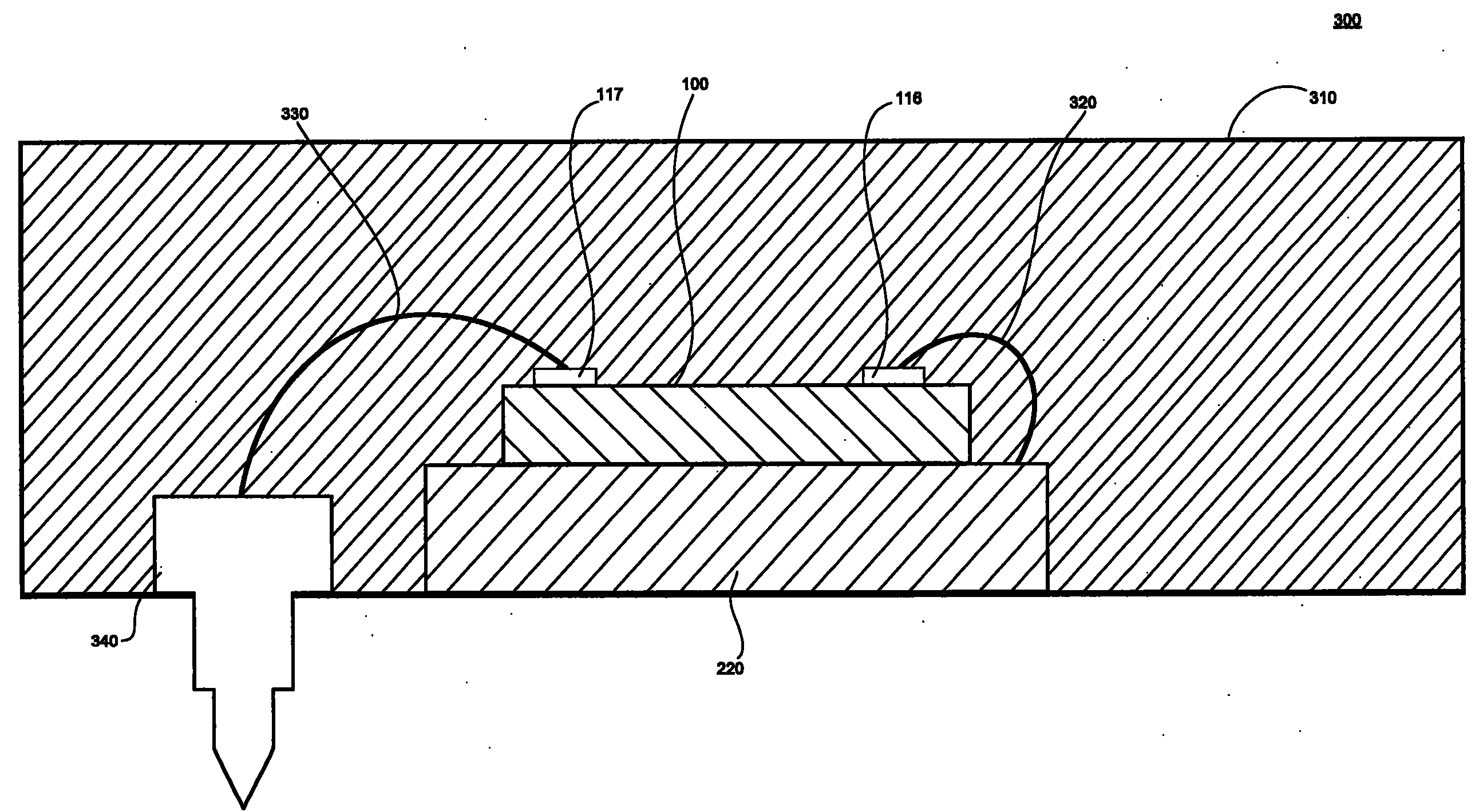
参阅图3,图3为本发明的集成电路的第一实施例侧视图。集成电路300包含有晶粒100、包覆体310、基底220、接脚340以及内联机330与下方焊接联机(down bond wire)320。晶粒100同样粘着于基底220之上,假设晶粒100具有多种功能,其中至少包含第一功能和第二功能,而且其上的接合垫111~115以及117~122是用来输出信号以及接收输入信号的信号接合垫,而接合垫116则为用来接收控制信号,以定义芯片100的功能的切换接合垫。如图所示,信号接合垫117由内联机330连接至集成电路300的接脚340,通过接脚340,接合垫117可以输出由晶粒100所产生的信号,也可以接收外部传至晶粒100的信号。接合垫111~115以及118~122也都分别通过其它的内联机来与其它的接脚相连。接合垫116则通过下方焊接联机320连接至基底220,使得接合垫116达到接地的效果,因此接合垫116便等同连接至一个低电压准位。接合垫116接收低电压准位的控制信号意谓着晶粒100工作于第一功能,也就是说,接合垫116不需通过接脚来接收控制信号。当使用者决定集成电路300的功能时,可以通过将接合垫116利用下方焊接联机320连结至基底220,来定义晶粒100的功能,因此可以节省集成电路300的封装接脚,以降低成本。包覆体310用来包覆晶粒100、基底220、内联机330、下方焊接联机320以及接脚340的上半部,接脚340的下半部则外露于包覆体310。在本发明较佳的实施例中,包覆体310可以是热固性塑料封胶或是塑料壳体。Referring to FIG. 3 , FIG. 3 is a side view of the first embodiment of the integrated circuit of the present invention. The
参阅图4,图4为本发明的集成电路的第二实施例侧视图。在集成电路400中,晶粒100的接合垫116没有连接至任何接脚或者基底,意谓着接合垫116上的电压准位呈现一高准位的状态,使得晶粒100工作于第二功能。Referring to FIG. 4 , FIG. 4 is a side view of the second embodiment of the integrated circuit of the present invention. In the integrated circuit 400, the
综上所述,具有多重功能的晶粒原本需要通过脚位来接收控制信号,进而决定晶粒的功能,在本发明中,晶粒上的接合垫可以不连接至任何脚位来将晶粒定义在第一种功能,而当要选择另一种功能时,只需利用下方焊接联机将晶粒的接合垫连接至基底。因此,集成电路在封装时可以至少省下一个接脚,降低整体的成本。To sum up, the chip with multiple functions originally needs to receive the control signal through the pin to determine the function of the chip. In the present invention, the bonding pad on the chip can not be connected to any pin to connect the chip The first function is defined, and when another function is selected, it is only necessary to connect the bonding pad of the die to the substrate using the soldering wire below. Therefore, at least one pin can be saved when the integrated circuit is packaged, reducing the overall cost.
当然,本发明还可有其它多种实施例,在不背离本发明精神及其实质的情况下,熟悉本领域的普通技术人员当可根据本发明做出各种相应的改变和变形,但这些相应的改变和变形都应属于本发明所附的权利要求的保护范围。Certainly, the present invention also can have other various embodiments, without departing from the spirit and essence of the present invention, those skilled in the art can make various corresponding changes and deformations according to the present invention, but these Corresponding changes and deformations should belong to the scope of protection of the appended claims of the present invention.
Claims (6)
Priority Applications (1)
| Application Number | Priority Date | Filing Date | Title |
|---|---|---|---|
| CNB2006101112300A CN100514619C (en) | 2006-08-15 | 2006-08-15 | Integrated circuit using under-bonding to define die functionality and method of making the same |
Applications Claiming Priority (1)
| Application Number | Priority Date | Filing Date | Title |
|---|---|---|---|
| CNB2006101112300A CN100514619C (en) | 2006-08-15 | 2006-08-15 | Integrated circuit using under-bonding to define die functionality and method of making the same |
Publications (2)
| Publication Number | Publication Date |
|---|---|
| CN101127341A CN101127341A (en) | 2008-02-20 |
| CN100514619C true CN100514619C (en) | 2009-07-15 |
Family
ID=39095319
Family Applications (1)
| Application Number | Title | Priority Date | Filing Date |
|---|---|---|---|
| CNB2006101112300A Expired - Fee Related CN100514619C (en) | 2006-08-15 | 2006-08-15 | Integrated circuit using under-bonding to define die functionality and method of making the same |
Country Status (1)
| Country | Link |
|---|---|
| CN (1) | CN100514619C (en) |
Citations (1)
| Publication number | Priority date | Publication date | Assignee | Title |
|---|---|---|---|---|
| CN1624918A (en) * | 2004-11-19 | 2005-06-08 | 威盛电子股份有限公司 | Multifunction chipset and related method |
-
2006
- 2006-08-15 CN CNB2006101112300A patent/CN100514619C/en not_active Expired - Fee Related
Patent Citations (1)
| Publication number | Priority date | Publication date | Assignee | Title |
|---|---|---|---|---|
| CN1624918A (en) * | 2004-11-19 | 2005-06-08 | 威盛电子股份有限公司 | Multifunction chipset and related method |
Also Published As
| Publication number | Publication date |
|---|---|
| CN101127341A (en) | 2008-02-20 |
Similar Documents
| Publication | Publication Date | Title |
|---|---|---|
| US6159765A (en) | Integrated circuit package having interchip bonding and method therefor | |
| US8115269B2 (en) | Integrated circuit package having reduced interconnects | |
| US6924496B2 (en) | Fingerprint sensor and interconnect | |
| US6933610B2 (en) | Method of bonding a semiconductor die without an ESD circuit and a separate ESD circuit to an external lead, and a semiconductor device made thereby | |
| US20070176278A1 (en) | Multi-chips stacked package | |
| US20020031873A1 (en) | Method and apparatus for implementing selected functionality on an integrated circuit device | |
| US6091138A (en) | Multi-chip packaging using bump technology | |
| CN102057481B (en) | Package with power and ground vias | |
| US10366934B2 (en) | Face down dual sided chip scale memory package | |
| CN100514619C (en) | Integrated circuit using under-bonding to define die functionality and method of making the same | |
| CN1954425B (en) | Programme to obtain pin map compatibility to semiconductor element | |
| KR20220128239A (en) | System in Package, SiP | |
| CN100524736C (en) | Stacked chip package structure | |
| JP3886905B2 (en) | Semiconductor parts with ESD protection | |
| KR101686140B1 (en) | Semiconductor chip package | |
| CN100466246C (en) | Flexible Substrates for Packaging | |
| TW200810030A (en) | Integrated circuit utilizing down bond to define the function of the die | |
| CN116072641A (en) | An isolated CUP pad | |
| US20120025898A1 (en) | Circuit Device | |
| JP4343727B2 (en) | Semiconductor device | |
| CN101577269B (en) | Multi-chip module and selection pad sharing method | |
| US20030227074A1 (en) | Semiconductor device | |
| US7196401B2 (en) | Chip-packaging with bonding options having a plurality of package substrates | |
| US20050248028A1 (en) | Chip-packaging with bonding options connected to a package substrate | |
| US9252119B1 (en) | Ball grid array including redistribution layer, packaged integrated circuit including the same, and methods of making and using the same |
Legal Events
| Date | Code | Title | Description |
|---|---|---|---|
| C06 | Publication | ||
| PB01 | Publication | ||
| C10 | Entry into substantive examination | ||
| SE01 | Entry into force of request for substantive examination | ||
| C14 | Grant of patent or utility model | ||
| GR01 | Patent grant | ||
| TR01 | Transfer of patent right |
Effective date of registration: 20191219 Address after: No.1, Duhang 1st Road, Hsinchu City, Hsinchu Science Park, Taiwan, China Patentee after: MEDIATEK Inc. Address before: Hsinchu County, Taiwan, China Patentee before: MSTAR SEMICONDUCTOR Inc. |
|
| TR01 | Transfer of patent right | ||
| CF01 | Termination of patent right due to non-payment of annual fee |
Granted publication date: 20090715 |
|
| CF01 | Termination of patent right due to non-payment of annual fee |