CN100473246C - Donor substrate for laser transfer and method of manufacturing organic light emitting display - Google Patents
Donor substrate for laser transfer and method of manufacturing organic light emitting display Download PDFInfo
- Publication number
- CN100473246C CN100473246C CNB2005100938018A CN200510093801A CN100473246C CN 100473246 C CN100473246 C CN 100473246C CN B2005100938018 A CNB2005100938018 A CN B2005100938018A CN 200510093801 A CN200510093801 A CN 200510093801A CN 100473246 C CN100473246 C CN 100473246C
- Authority
- CN
- China
- Prior art keywords
- layer
- organic
- donor substrate
- group
- substrate
- Prior art date
- Legal status (The legal status is an assumption and is not a legal conclusion. Google has not performed a legal analysis and makes no representation as to the accuracy of the status listed.)
- Expired - Fee Related
Links
Images


Classifications
-
- H—ELECTRICITY
- H05—ELECTRIC TECHNIQUES NOT OTHERWISE PROVIDED FOR
- H05B—ELECTRIC HEATING; ELECTRIC LIGHT SOURCES NOT OTHERWISE PROVIDED FOR; CIRCUIT ARRANGEMENTS FOR ELECTRIC LIGHT SOURCES, IN GENERAL
- H05B33/00—Electroluminescent light sources
- H05B33/10—Apparatus or processes specially adapted to the manufacture of electroluminescent light sources
-
- B—PERFORMING OPERATIONS; TRANSPORTING
- B41—PRINTING; LINING MACHINES; TYPEWRITERS; STAMPS
- B41M—PRINTING, DUPLICATING, MARKING, OR COPYING PROCESSES; COLOUR PRINTING
- B41M5/00—Duplicating or marking methods; Sheet materials for use therein
- B41M5/26—Thermography ; Marking by high energetic means, e.g. laser otherwise than by burning, and characterised by the material used
- B41M5/265—Thermography ; Marking by high energetic means, e.g. laser otherwise than by burning, and characterised by the material used for the production of optical filters or electrical components
-
- B—PERFORMING OPERATIONS; TRANSPORTING
- B41—PRINTING; LINING MACHINES; TYPEWRITERS; STAMPS
- B41M—PRINTING, DUPLICATING, MARKING, OR COPYING PROCESSES; COLOUR PRINTING
- B41M5/00—Duplicating or marking methods; Sheet materials for use therein
- B41M5/26—Thermography ; Marking by high energetic means, e.g. laser otherwise than by burning, and characterised by the material used
- B41M5/382—Contact thermal transfer or sublimation processes
- B41M5/38207—Contact thermal transfer or sublimation processes characterised by aspects not provided for in groups B41M5/385 - B41M5/395
- B41M5/38214—Structural details, e.g. multilayer systems
-
- H—ELECTRICITY
- H10—SEMICONDUCTOR DEVICES; ELECTRIC SOLID-STATE DEVICES NOT OTHERWISE PROVIDED FOR
- H10K—ORGANIC ELECTRIC SOLID-STATE DEVICES
- H10K71/00—Manufacture or treatment specially adapted for the organic devices covered by this subclass
- H10K71/10—Deposition of organic active material
- H10K71/18—Deposition of organic active material using non-liquid printing techniques, e.g. thermal transfer printing from a donor sheet
-
- H—ELECTRICITY
- H10—SEMICONDUCTOR DEVICES; ELECTRIC SOLID-STATE DEVICES NOT OTHERWISE PROVIDED FOR
- H10K—ORGANIC ELECTRIC SOLID-STATE DEVICES
- H10K71/00—Manufacture or treatment specially adapted for the organic devices covered by this subclass
- H10K71/60—Forming conductive regions or layers, e.g. electrodes
-
- H—ELECTRICITY
- H10—SEMICONDUCTOR DEVICES; ELECTRIC SOLID-STATE DEVICES NOT OTHERWISE PROVIDED FOR
- H10K—ORGANIC ELECTRIC SOLID-STATE DEVICES
- H10K71/00—Manufacture or treatment specially adapted for the organic devices covered by this subclass
-
- H—ELECTRICITY
- H10—SEMICONDUCTOR DEVICES; ELECTRIC SOLID-STATE DEVICES NOT OTHERWISE PROVIDED FOR
- H10K—ORGANIC ELECTRIC SOLID-STATE DEVICES
- H10K71/00—Manufacture or treatment specially adapted for the organic devices covered by this subclass
- H10K71/40—Thermal treatment, e.g. annealing in the presence of a solvent vapour
- H10K71/421—Thermal treatment, e.g. annealing in the presence of a solvent vapour using coherent electromagnetic radiation, e.g. laser annealing
-
- Y—GENERAL TAGGING OF NEW TECHNOLOGICAL DEVELOPMENTS; GENERAL TAGGING OF CROSS-SECTIONAL TECHNOLOGIES SPANNING OVER SEVERAL SECTIONS OF THE IPC; TECHNICAL SUBJECTS COVERED BY FORMER USPC CROSS-REFERENCE ART COLLECTIONS [XRACs] AND DIGESTS
- Y10—TECHNICAL SUBJECTS COVERED BY FORMER USPC
- Y10T—TECHNICAL SUBJECTS COVERED BY FORMER US CLASSIFICATION
- Y10T156/00—Adhesive bonding and miscellaneous chemical manufacture
- Y10T156/17—Surface bonding means and/or assemblymeans with work feeding or handling means
- Y10T156/1702—For plural parts or plural areas of single part
- Y10T156/1705—Lamina transferred to base from adhered flexible web or sheet type carrier
Landscapes
- Engineering & Computer Science (AREA)
- Manufacturing & Machinery (AREA)
- Physics & Mathematics (AREA)
- Optics & Photonics (AREA)
- Electroluminescent Light Sources (AREA)
- Printers Or Recording Devices Using Electromagnetic And Radiation Means (AREA)
Abstract
提供了一种用于激光转写(LITI)的施主基板和一种使用该施主基板制造有机发光显示器的方法。将导电框架设置在施主基板的外部上并与防静电层相连接。施主基板的导电框架与接地台相连接。在这个结构中,当用LITI工艺形成有机层时,可控制静电的产生。
Provided are a donor substrate for laser transfer inscription (LITI) and a method of manufacturing an organic light emitting display using the donor substrate. A conductive frame is disposed on the exterior of the donor substrate and connected to the antistatic layer. The conductive frame of the donor substrate is connected to the ground plane. In this structure, when the organic layer is formed by the LITI process, generation of static electricity can be controlled.
Description
技术领域 technical field
本发明涉及一种用于激光转写(LITI)的施主基板以及一种用该基板制造有机发光显示器(OLED)的方法,更具体地讲,涉及一种用于LITI的施主基板以及用该基板制造OLED的方法,该基板可控制静电的产生。The present invention relates to a kind of donor substrate for laser transfer writing (LITI) and a kind of method using this substrate to manufacture organic light-emitting display (OLED), more particularly, relates to a kind of donor substrate for LITI and using this substrate A method of manufacturing an OLED, a substrate that controls the generation of static electricity.
背景技术 Background technique
近年来,由于OLED耗电低,并且发光效率高、视角宽、响应速度快,因此非常适合作为显示高分辨率的运动图像的介质。In recent years, OLEDs are very suitable as a medium for displaying high-resolution moving images due to their low power consumption, high luminous efficiency, wide viewing angle, and fast response speed.
另外,OLED包括有机层,该有机层包括设置于阳极与阴极之间的有机发射层。OLED是自发射显示,在OLED中,当在阴极与阳极之间施加电压时,电子与空穴在有机发射层中相结合以产生光。由于OLED不像液晶显示器(LCD)那样需要背光,所以可通过简单的工艺制造成轻而薄的样式。In addition, OLEDs include organic layers including an organic emissive layer disposed between an anode and a cathode. OLEDs are self-emissive displays in which electrons and holes combine in an organic emissive layer to generate light when a voltage is applied between a cathode and an anode. Since OLED does not require a backlight like a liquid crystal display (LCD), it can be manufactured in a light and thin form through a simple process.
在这种情况下,根据有机层(特别是,有机发射层)的材料,OLED可被分成小分子OLED和高分子OLED。In this case, OLEDs may be classified into small-molecule OLEDs and high-molecule OLEDs according to materials of organic layers (in particular, organic emission layers).
小分子OLED包括位于阳极与阴极之间的具有不同功能的多层有机层,如空穴注入层、空穴输送层、发射层、空穴阻碍层、电子注入层。为防止电荷积聚,可执行掺杂处理或可使用具有适当能级的材料来替代。在这种情况下,由于上述有机层通常由真空沉积的方法形成,因此很难实现大尺寸的显示器。Small molecule OLEDs include multilayer organic layers with different functions located between the anode and the cathode, such as hole injection layer, hole transport layer, emission layer, hole blocking layer, and electron injection layer. To prevent charge accumulation, a doping process may be performed or a material having an appropriate energy level may be used instead. In this case, since the above-mentioned organic layers are generally formed by a vacuum deposition method, it is difficult to realize a large-sized display.
另一方面,高分子OLED包括在阳极与阴极之间有机发射层的单一结构或有机发射层和空穴输送层的双重结构。因此,高分子OLED可被制成具有较小的厚度。另外,由于有机层是用湿涂工艺形成,因此可在常压下形成,从而可大大降低生产成本,且易于制造大面积的OLED。On the other hand, a polymer OLED includes a single structure of an organic emission layer between an anode and a cathode or a dual structure of an organic emission layer and a hole transport layer. Therefore, polymer OLEDs can be made to have a smaller thickness. In addition, since the organic layer is formed by a wet coating process, it can be formed under normal pressure, thereby greatly reducing production costs and making it easy to manufacture large-area OLEDs.
在制造单色装置的过程中,高分子OLED可使用旋转工艺来简单地制造,但是产量和使用期限比小分子OLED低。另外,全色装置可通过在OLED上将红(R)、绿(G)、篮(B)色发射层图案化来制造。这里,使用荫罩通过沉积方法可将小分子OLED的有机层图案化,然而,通过喷墨印刷工艺或激光转写(LITI)工艺可将高分子OLED的有机层图案化。由于LITI工艺直接利用旋涂工艺的特点,因此,当形成大面积的有机层时,可提高象素的均匀性。另外,由于LITI工艺不是湿法工艺而是干法工艺,因此,可克服由于溶剂造成的OLED的使用期限的减少,并将有机层精细地图案化。In the process of manufacturing monochrome devices, polymer OLEDs can be simply fabricated using a spin process, but yields and lifetimes are lower than those of small molecule OLEDs. Additionally, full-color devices can be fabricated by patterning red (R), green (G), and blue (B) color emitting layers on OLEDs. Here, the organic layer of the small molecule OLED may be patterned by a deposition method using a shadow mask, however, the organic layer of the high molecule OLED may be patterned by an inkjet printing process or a laser transfer (LITI) process. Since the LITI process directly utilizes the characteristics of the spin-coating process, it can improve the uniformity of the pixel when forming a large-area organic layer. In addition, since the LITI process is not a wet process but a dry process, it is possible to overcome the decrease in lifetime of the OLED due to the solvent and finely pattern the organic layer.
LITI工艺的应用主要需要:光源、OLED基板、施主基板。施主基板包括:基层、光热转化(LTHC)层和输送层。The application of LITI process mainly requires: light source, OLED substrate, donor substrate. The donor substrate includes: a base layer, a light-to-heat conversion (LTHC) layer and a transport layer.
在LITI工艺过程中,光从光源中发出并被吸收到LTHC层中,因此将光转变成热能,从而由于热能可将在输送层上形成的有机材料输送到基板上。During the LITI process, light is emitted from a light source and absorbed into the LTHC layer, thus converting the light into thermal energy, whereby the organic material formed on the transport layer can be transported to the substrate due to the thermal energy.
用LITI工艺将OLED上的有机层图案化的方法,不仅在韩国专利登记第10-0342653号中公开,还在美国专利第5,998,085号、第6,214,520号、第6,114,085号中公开。The method of patterning the organic layer on the OLED by the LITI process is disclosed not only in Korean Patent Registration No. 10-0342653 but also in US Patent Nos. 5,998,085, 6,214,520, and 6,114,085.
图1A至1C为示出用LITI工艺将有机层23图案化的方法的剖视图。1A to 1C are cross-sectional views illustrating a method of patterning an
参考图1A,提供了基板10,并在基板10上层叠着施主基板20,该施主基板20包括基层21、LTHC层22和有机层23。Referring to FIG. 1A , a
参考图1B,将激光束照射到第一区域(a)中的施主基板20的基层21上。透射穿过基层21的激光束被转化成LTHC层中的热。由于该热,使得第一区域(a)中的有机层23与LTHC层22的粘附力减弱。Referring to FIG. 1B , a laser beam is irradiated onto the
参考图1C,在第一区域(a)中的有机层23被输送到基板10上之后,该有机层与LTHC层22的粘附较差,施主基板20与基板10分离。因此,将有机层23a在基板10上图案化,并且第二区域(b)(即,未被照射激光束的区域)中的有机层23b与施主基板20一起与基板10分离。结果,完成有机输送图案23a。Referring to FIG. 1C , after the
但是,在用上述LITI工艺形成有机输送图案23a的过程中,在将施主基板20附着于基板10或将施主基板20与基板10分离的过程中,由于摩擦和外部环境因素可产生静电。由于在静电放电期间,电压可达到几千至几万,所以连接可出现短路,由于OLED温度的上升,金属层可被融化,或者连接线被断开。即,在OLED中可发生故障,反过来可影响OLED中的内部电路,使OLED的性能降低。However, static electricity may be generated due to friction and external environmental factors during the process of attaching or detaching the
发明内容 Contents of the invention
因此,本发明提供了一种制造有机发光显示器(OLED)的方法,该方法可以控制当用激光转写(LITI)工艺形成有机层时的静电产生。Accordingly, the present invention provides a method of manufacturing an organic light emitting display (OLED) that can control static electricity generation when an organic layer is formed using a laser transfer writing (LITI) process.
在本发明的示例性实施例中,一种用于LITI的施主基板包括:基层;光热转化(LTHC)层,置于基层的整个表面上;防静电层,置于光热转化层的整个表面上;输送层,置于防静电层的整个表面上;导电框架,置于施主基板的外部,并与防静电层相连接。In an exemplary embodiment of the present invention, a donor substrate for LITI includes: a base layer; a light-to-heat conversion (LTHC) layer placed on the entire surface of the base layer; an antistatic layer placed on the entire surface of the light-to-heat conversion layer on the surface; a transport layer placed on the entire surface of the antistatic layer; a conductive frame placed on the outside of the donor substrate and connected to the antistatic layer.
在本发明的另一个示例性实施例中,一种制造用于LITI的施主基板的方法包括:提供基层;在基层的整个表面上形成光热转化层;在光热转化层的整个表面上形成防静电层;在防静电层上形成输送层;在合成的施主基板的外部上形成导电框架。其中,所述防静电层与所述框架相连接。In another exemplary embodiment of the present invention, a method of manufacturing a donor substrate for LITI includes: providing a base layer; forming a light-to-heat conversion layer on the entire surface of the base layer; forming An antistatic layer; a transport layer formed on the antistatic layer; a conductive frame formed on the exterior of the composite donor substrate. Wherein, the antistatic layer is connected with the frame.
在本发明的另一个示例性实施例中,一种制造OLED的方法包括:将第一电极在基板上图案化;将基板固定地吸附到可输送并接地的台上;通过选择性地将激光束照射在施主基板上,将至少包括发射层的有机层输送到施主基板;将施主基板与基板分离;在包含有机层的基板的整个表面上形成第二电极。In another exemplary embodiment of the present invention, a method of manufacturing an OLED includes: patterning a first electrode on a substrate; fixedly attaching the substrate to a transportable and grounded stage; The beam is irradiated on the donor substrate, the organic layer including at least the emitting layer is transferred to the donor substrate; the donor substrate is separated from the substrate; and the second electrode is formed on the entire surface of the substrate including the organic layer.
在本发明的另一个示例性实施例中,提供了一种根据上述方法制造OLED的方法。In another exemplary embodiment of the present invention, a method of manufacturing an OLED according to the above method is provided.
附图说明 Description of drawings
将参照附图来详细描述本发明的优选实施例,本发明的上述及其它优点会变得更加清楚,其中:Preferred embodiments of the present invention will be described in detail with reference to the accompanying drawings, and the above-mentioned and other advantages of the present invention will become more apparent, wherein:
图1A至1C为示出了用激光转写(LITI)方法使有机层图案化的工艺的剖视图;1A to 1C are cross-sectional views illustrating a process of patterning an organic layer by a laser transfer writing (LITI) method;
图2为根据本发明示例性实施例的施主基板的剖视图;2 is a cross-sectional view of a donor substrate according to an exemplary embodiment of the present invention;
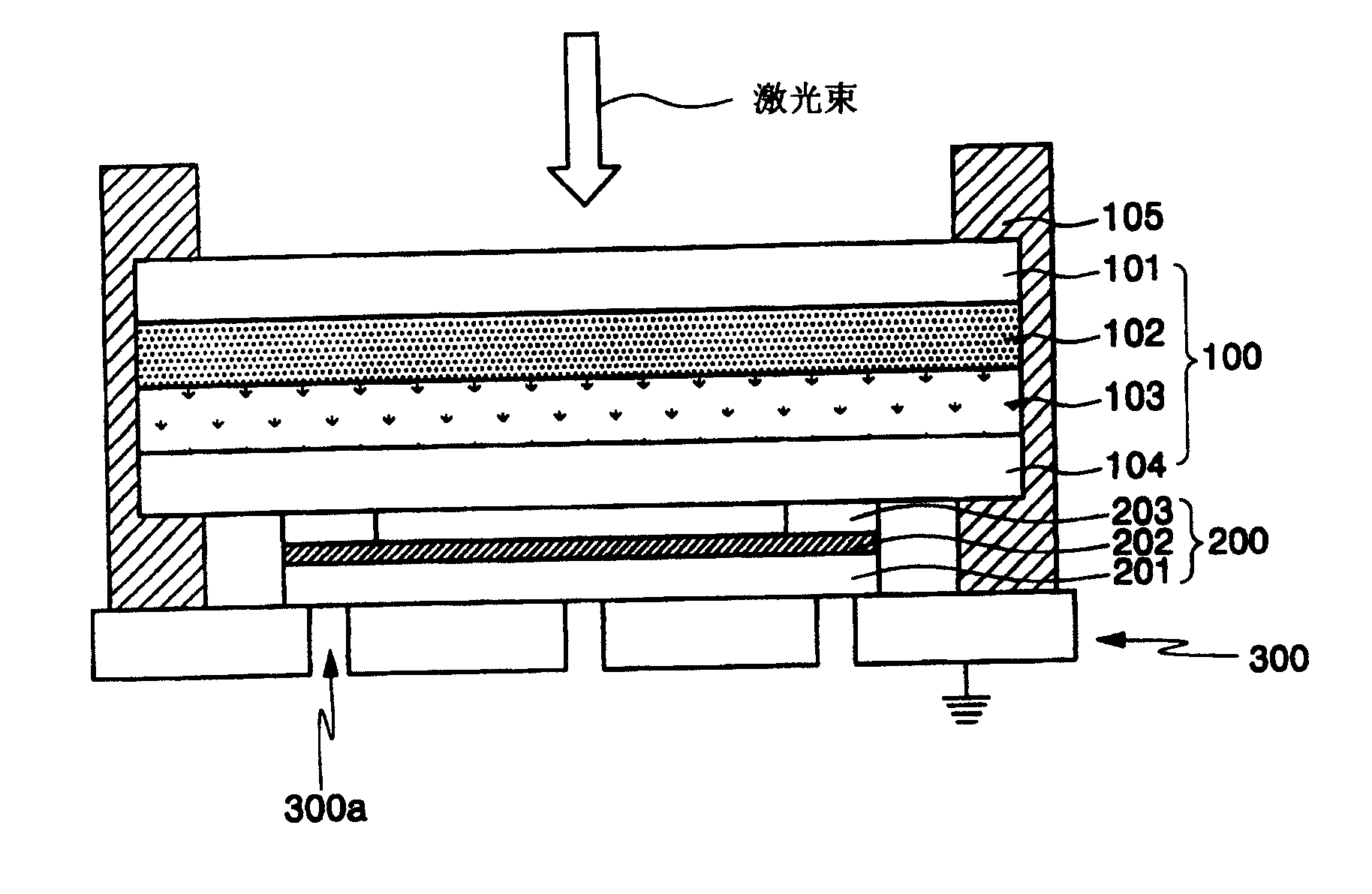
图3A至图3C为示出了根据本发明示例性实施例制造有机发光显示器(OLED)的方法的剖视图。3A to 3C are cross-sectional views illustrating a method of manufacturing an organic light emitting display (OLED) according to an exemplary embodiment of the present invention.
具体实施方式 Detailed ways
以下将参照附图来更充分地描述本发明,在所述附图中示出了本发明的示例性实施例。The present invention will be described more fully hereinafter with reference to the accompanying drawings, in which exemplary embodiments of the invention are shown.
图2为根据本发明示例性实施例的施主基板100的剖视图。FIG. 2 is a cross-sectional view of a
参考图2,施主基板100包括:基层101、光热转化(LTHC)层102、防静电层103和输送层104,这些层顺序地叠放在基层101上。将由导电材料形成的框架附于施主基板100的外部。Referring to FIG. 2 , the
基层101应该是透明的,这样光被透射到LTHC层102。基层101可由具有适当的光学性能和足够的机械稳定性的聚合物形成。基层101可由从聚酯、聚丙烯酸、聚环氧、聚乙烯和聚苯乙烯组成的组中选择至少一种聚合物形成。更优选的是,基层101可由聚对苯二甲酸乙二醇酯(PET)形成。The
LTHC层102吸收红外(IR)-可见(V)区域的光,并将部分光转化为热。LTHC层102应该具有适当的光学密度,且可由吸光材料形成以吸收光。这里,LTHC层102可为由Al、Ag、及其氧化物或硫化物形成的金属层,或为由碳黑、石墨、或IR染料形成的聚合物有机层。金属层可用真空沉积法、电子束(e-beam)沉积法或溅射法来形成,有机层可由常用的薄膜涂布法形成,例如,辊式涂布工艺、凹版印刷工艺、挤压工艺、旋涂工艺,和刮涂工艺之一。The
防静电层(夹层)103可起抑制静电的作用,当将施主基板100附于基板(未示出)时,或在LITI工艺之后将施主基板100与基板分离时,产生所述静电。施主基板100的防静电层103与框架105相连接,框架105与接地台(grounded stage)相连接,从而抑制静电的产生。防静电层103可由从有机材料、无机材料及其混合物组成的组中选择一种形成。例如,所述有机材料可以是从由聚苯胺、聚吡咯、聚噻吩,和聚(3,4二氧乙基噻吩)组成的组中选择的一种导电聚合物。当防静电层103由导电聚合物形成时,通过湿涂工艺该防静电层可形成均匀的厚度。另外,所述无机材料可以是从由锑锡氧化物(ATO)、铟锡氧化物(ITO)、铟锌氧化物(IZO)、Nb2O3、ZnO、TiN组成的组中选择的一种材料。当防静电层103由无机材料形成时,该防静电层103可以是高导电的,可有效地控制静电,并具有耐用性。另外,所述有机材料与无机材料的混合物可以是从由ATO溶胶、ITO溶胶、Ag-Pd和Ag-Ru组成的组中选择的一种材料。由于所述有机材料与无机材料的混合物是溶胶状态,因此,有利于薄层的形成和导电性的增加。The antistatic layer (interlayer) 103 may function to suppress static electricity that is generated when the
输送层104可以是从有机发射层、有机空穴注入层、有机空穴输送层、有机空穴阻碍层、有机电子注入层、有机电子输送层及这些层的叠层组成的组中选择的一个层。The
输送层140可通过挤压工艺、旋涂工艺、刮涂工艺、真空沉积工艺、或化学气相沉积(CVD)工艺形成。The transport layer 140 may be formed through an extrusion process, a spin coating process, a blade coating process, a vacuum deposition process, or a chemical vapor deposition (CVD) process.
另外,在防静电层103和输送层104之间可另外地设置中间层,以提高输送特性。在这种情况下,中间层可包括气体发生层、缓冲层和金属反射层中的至少一个。In addition, an intermediate layer may be additionally provided between the
气体发生层吸收光或热,并引起分解反应,从而发出N2气以提供输送能。气体发生层可由季戊四醇四硝酸酯或三硝基甲苯形成。The gas generating layer absorbs light or heat, and causes a decomposition reaction, thereby emitting N2 gas to provide transport energy. The gas generating layer may be formed of pentaerythritol tetranitrate or trinitrotoluene.
缓冲层的作用是防止光热吸收材料污染或破坏输送层104,该输送层将在随后的工艺中形成。另外,缓冲层控制防静电层103与输送层104的粘合,从而改善输送图案的特性。这里,缓冲层可由金属氧化物、无机非金属化合物、或惰性聚合物形成。The function of the buffer layer is to prevent the light-heat absorbing material from polluting or damaging the
金属反射层反射照射到施主基板100的基层101上的激光束,从而给LTHC层102提供更多的能量。另外,当另外地设置气体发生层时,金属反射层的作用是防止由气体发生层产生的气体扩散至输送层104中。The metal reflective layer reflects the laser beam irradiated on the
如上所述,附于施主基板100的外部的框架105可由导电材料形成。在这种情况下,导电材料可以是有机材料、无机材料,及其混合物之一。例如,所述有机材料可以是从由聚苯胺、聚吡咯、聚噻吩,和聚(3,4二氧乙基噻吩)组成的组中选择的一种导电聚合物。另外,所述无机材料可以是从由ATO、ITO、IZO、Nb2O3、ZnO和TiN组成的组中选择的一种材料。当框架105是由无机材料形成时,该框架可以是高导电的,可有效地控制静电,并具有耐用性。另外,所述有机材料与无机材料的混合物可以是从由ATO溶胶、ITO溶胶、Ag-Pd和Ag-Ru组成的组中选择的一种材料。As described above, the
施主基板100的输送层104与框架105直接连接或电连接。在LITI工艺过程中,框架105与接地台连接,从而控制由LITI工艺引起的静电。The
在这种情况下,框架105使施主基板100保持平展。因此,可将基板粘结到施主基板100上,在随后的LITI工艺中不会在施主基板100中下垂。结果,改善了输送特性。另外,在用LITI工艺形成输送层104之后,施主基板100利用框架105易于与基板分离。In this case, the
下面,将参考图3A至3C描述根据本发明示例性实施例的使用施主基板通过LITI工艺制作的有机发光显示器(OLED)的方法。Hereinafter, a method of an organic light emitting display (OLED) fabricated through a LITI process using a donor substrate according to an exemplary embodiment of the present invention will be described with reference to FIGS. 3A to 3C .
参考图3A,基板吸入(suction)台300,在其上设置接地的基板200。Referring to FIG. 3A , a
这里,基板200包括:第一电极202,该电极利用通常的方法形成在绝缘基板201上;象素限定层203,该层形成在第一电极202上以限定象素部分。另外,基板200可以包括薄膜晶体管(TFT)和多个绝缘层。当第一电极202为阳极时,它可以是透明电极,该透明电极由具有高功函(high workfunction)的金属如ITO或IZO等形成;或者可以是反射电极,该反射电极可从由Pt、Au、Ir、Cr、Mg、Ag、Ni、Al及它们的合金组成的组中选择的一种材料形成。Here, the
当第一电极202为阴极时,可以是薄透明电极,或者为厚的反射电极,该透明电极由具有低功函的金属形成,所述金属可从由Mg、Ca、Al、Ag、Ba及它们的合金组成的组中选择。When the
与此同时,基板吸入台300是接地的,并且是这样的单元,用吸入部分300a固定地吸收并移动基板200。Meanwhile, the
另外,根据本发明示例性实施例制造具有外部的施主基板100,其外部被附着了导电框架105。施主基板100包括:基层101、LTHC层102、防静电层103和输送层104。这里,防静电层103可与框架105相连接。In addition, a
参考图3B,将具有框架105的施主基板100粘结到基板200上,该基板200被吸附并固定到台300,从而施主基板100面对基板200的象素区域。在这种情况下,施主基板100的防静电层103可与框架105相连接,且框架105可与接地台300相连接。Referring to FIG. 3B , the
然后,将激光束照射到施主基板100的预定区域上,从而将输送层104输送到第一电极202的象素区域上。Then, a laser beam is irradiated onto a predetermined area of the
在这种情况下,输送层104包括至少一个有机发射层,并且还可包括从有机空穴注入层、有机空穴输送层、有机空穴阻碍层、有机电子输送层、有机电子注入层组成的组中选择的至少一个层以提高OLED的性能。In this case, the
有机发射层可由红色发光材料形成,该材料是小分子材料,如Alq3(主体)/DCJTB(荧光掺杂物)、Alq3(主体)/DCM(荧光掺杂物)、CBP(主体)/PtOEP(荧光体有机金属络合物),或者聚合物,如PFO基的聚合物和PPV基的聚合物。有机发射层可由绿色发光材料形成,该材料是小分子材料,如Alq3、Alq3(主体)/C545t(掺杂物)、CBP(主体)/IrPPy(荧光体有机金属络合物),或者聚合物,如PFO基的聚合物和PPV基的聚合物。另外,有机发射层可由蓝色发光材料形成,该材料是小分子材料,如DPVBi、螺旋DPVBi,螺旋6P、蒸馏苯(DSB)、蒸馏芳香基化合物(distilled arylene)(DSA)或者聚合物,如PFO基的聚合物和PPV基的聚合物。The organic emission layer can be formed by a red luminescent material, which is a small molecule material, such as Alq3 (host)/DCJTB (fluorescent dopant), Alq3 (host)/DCM (fluorescent dopant), CBP (host)/PtOEP ( Phosphor organometallic complexes), or polymers, such as PFO-based polymers and PPV-based polymers. The organic emission layer can be formed of a green light-emitting material, which is a small molecule material such as Alq3, Alq3 (host)/C545t (dopant), CBP (host)/IrPPy (phosphor organometallic complex), or a polymer , such as PFO-based polymers and PPV-based polymers. In addition, the organic emission layer may be formed of a blue light-emitting material, which is a small molecule material such as DPVBi, helical DPVBi, helical 6P, distilled benzene (DSB), distilled arylene (DSA) or a polymer such as PFO-based polymers and PPV-based polymers.
当第一电极202为阳极时,空穴注入层在第一电极202上形成。在这种情况下,为了便于空穴的注入并提高OLED的使用期间,空穴注入层是由与第一电极202紧密地粘结、需要低电离能的材料形成。空穴注入层可由芳基胺化合物(aryl amine compound)、卟啉基金属络合物、或星芒胺(starburst amine)形成。更具体地讲,空穴注入层可由4,4’,4”-三(3-甲基苯基-苯基胺基)-三苯胺(m-MTDATA)、1,3,5-三[4-(3-甲基-苯基-苯基-胺基)苯基]苯(m-MTDATB)、或酞菁铜(CuPc)形成。When the
空穴输送层易于将空穴输送到发射层,并抑制由第二电极(未示出)产生的电子移动到发射区域,从而提高OLED的发光效率。空穴输送层可由亚芳基二(元)胺衍生物、星芒化合物、有螺旋基衍生物联苯二(元)胺、或梯形化合物形成。更具体地讲,空穴输送层可由N,N-联苯基-N,N’-双(4-甲基-苯基)-1,1’-联苯基-4,4’-二(元)胺(TPD)、或4,4’-双[N-(1-萘基)-苯基-胺基]联苯基(NPB)形成。The hole transport layer easily transports holes to the emission layer, and suppresses electrons generated from the second electrode (not shown) from moving to the emission region, thereby improving luminous efficiency of the OLED. The hole transport layer can be formed of arylene di(yuan)amine derivatives, starburst compounds, helicyl derivatives biphenyldi(yuan)amines, or ladder compounds. More specifically, the hole transport layer can be made of N,N-biphenyl-N,N'-bis(4-methyl-phenyl)-1,1'-biphenyl-4,4'-bis( Yuan) amine (TPD), or 4,4'-bis[N-(1-naphthyl)-phenyl-amino]biphenyl (NPB).
由于在有机发射层中空穴迁移率比电子迁移率高,且在发射层中形成的激发子被扩散到宽范围,因此可降低发光效率,空穴阻碍层防止该发光效率降低。空穴阻碍层可从由2-联苯基-4-基-5-(4-叔丁基苯基)-1,3,4-氧化重氮盐(PBD)、螺旋-PBD、3-(4’-叔丁基苯基)-4-苯基-5-(4’-联苯基)-1,2,4-三唑(TAZ)组成的组中选择的一个形成。Since hole mobility is higher than electron mobility in the organic emission layer, and excitons formed in the emission layer are diffused over a wide range, luminous efficiency may be reduced, and the hole blocking layer prevents this reduction in luminous efficiency. The hole blocking layer can be formed from 2-biphenyl-4-base-5-(4-tert-butylphenyl)-1,3,4-oxidized diazonium salt (PBD), helix-PBD, 3-( One selected from the group consisting of 4'-tert-butylphenyl)-4-phenyl-5-(4'-biphenylyl)-1,2,4-triazole (TAZ) is formed.
电子输送层可堆叠在有机发射层上,并可由可接受电子的金属化合物形成。例如,电子输送层可由8-(氢化喹啉)铝(Alq3)形成,该材料可稳定地接收从第二电极输送的电子。The electron transport layer may be stacked on the organic emission layer, and may be formed of an electron-acceptable metal compound. For example, the electron transport layer may be formed of 8-(hydroquinoline)aluminum (Alq3), which can stably receive electrons transported from the second electrode.
在这种情况下,可通过旋涂工艺或沉积工艺形成有机层。或者,当用LITI工艺在施主基板100上形成输送层104时,可同时形成有机发射层和有机层之一。In this case, the organic layer may be formed through a spin coating process or a deposition process. Alternatively, when the
参考图3C,在输送层104被输送到第一电极202上之后,施主基板100与基板200分离,从而形成有机层图案104’。因此,第二电极204在有机层图案104’上形成。尽管在附图中没有示出,用封装基板或金属罐将合成结构(resultant structure)封装,从而完成OLED。Referring to FIG. 3C, after the
当第二电极204为阴极时,可以是薄透明电极,该透明电极由具有低功函的金属形成,该金属可从由Mg、Ca、Al、Ag及其合金组成的组中选择一种;或者可以为反射电极。When the
另外,当第二电极204为阳极时,可以为透明电极,该透明电极由具有如ITO或IZO的高功函的金属形成;或者可以为反射电极,该反射电极由从Pt、Au、Ir、Cr、Mg、Ag、Ni、Al及它们的合金组成的组中选择的一种材料形成。In addition, when the
如上所述,本发明有效地控制静电,该静电可发生在用LITI工艺在制造OLED的过程中。因此,防止由于静电导致的OLED的退化,从而实现高质量的OLED。As described above, the present invention effectively controls static electricity that may occur during the manufacture of OLEDs using the LITI process. Accordingly, degradation of the OLED due to static electricity is prevented, thereby realizing a high-quality OLED.
另外,在本发明中,框架在施主基板的外部上形成。因此,输送层可通过LITI工艺有效地形成,且施主基板可易于与基板粘结或分离,以提高导电性。In addition, in the present invention, the frame is formed on the outside of the donor substrate. Therefore, the transport layer can be efficiently formed through the LITI process, and the donor substrate can be easily bonded or separated from the substrate to improve conductivity.
尽管已经参照本发明的确定的示例性实施例描述了本发明,但本领域的技术人员应该清楚,在不脱离权利要求及其等同物所限定的本发明的精神或范围的情况下,对本发明可作各种修改和变形。While the invention has been described with reference to certain exemplary embodiments of the invention, it should be apparent to those skilled in the art that the invention can be modified without departing from the spirit or scope of the invention as defined in the claims and their equivalents. Various modifications and variations are possible.
本申请要求2004年8月30日提交的第2004-68774号韩国专利申请的优先权,该文献的全部内容以引用的方法包含于此。This application claims priority from Korean Patent Application No. 2004-68774 filed on Aug. 30, 2004, the entire contents of which are hereby incorporated by reference.
Claims (30)
Applications Claiming Priority (2)
| Application Number | Priority Date | Filing Date | Title |
|---|---|---|---|
| KR1020040068774A KR100623694B1 (en) | 2004-08-30 | 2004-08-30 | Donor substrate for laser transfer and manufacturing method of organic electroluminescent element manufactured using this substrate |
| KR1020040068774 | 2004-08-30 |
Publications (2)
| Publication Number | Publication Date |
|---|---|
| CN1758818A CN1758818A (en) | 2006-04-12 |
| CN100473246C true CN100473246C (en) | 2009-03-25 |
Family
ID=36153880
Family Applications (1)
| Application Number | Title | Priority Date | Filing Date |
|---|---|---|---|
| CNB2005100938018A Expired - Fee Related CN100473246C (en) | 2004-08-30 | 2005-08-30 | Donor substrate for laser transfer and method of manufacturing organic light emitting display |
Country Status (6)
| Country | Link |
|---|---|
| US (2) | US7294444B2 (en) |
| EP (1) | EP1629990B1 (en) |
| JP (1) | JP4292241B2 (en) |
| KR (1) | KR100623694B1 (en) |
| CN (1) | CN100473246C (en) |
| DE (1) | DE602005004210T2 (en) |
Families Citing this family (21)
| Publication number | Priority date | Publication date | Assignee | Title |
|---|---|---|---|---|
| KR20060033554A (en) * | 2004-10-15 | 2006-04-19 | 삼성에스디아이 주식회사 | Laser thermal transfer device and manufacturing method of organic electroluminescent device using same |
| KR101194646B1 (en) * | 2005-12-30 | 2012-10-24 | 엘지디스플레이 주식회사 | Fabricating method of soft mold |
| TW200908784A (en) * | 2007-04-27 | 2009-02-16 | Nagase & Amp Co Ltd | Method for manufacturing organic el display |
| JP5150138B2 (en) * | 2007-05-23 | 2013-02-20 | 株式会社ジャパンディスプレイイースト | Manufacturing method of display device |
| KR101563237B1 (en) * | 2007-06-01 | 2015-10-26 | 가부시키가이샤 한도오따이 에네루기 켄큐쇼 | Manufacturing apparatus and manufacturing method of light-emitting device |
| KR100959111B1 (en) * | 2008-03-27 | 2010-05-25 | 삼성모바일디스플레이주식회사 | Manufacturing apparatus and manufacturing method of organic light emitting device |
| JP2011170200A (en) * | 2010-02-19 | 2011-09-01 | Seiko Instruments Inc | Liquid crystal device and method of manufacturing liquid crystal device |
| US10526198B2 (en) * | 2011-03-04 | 2020-01-07 | Texas Instruments Incorporated | Infrared sensor design using an epoxy film as an infrared absorption layer |
| KR20130010624A (en) * | 2011-07-19 | 2013-01-29 | 삼성디스플레이 주식회사 | Donor substrate, method of manufacturing a donor substrate and method of manufacturing an organic light emitting display device using a donor substrate |
| WO2013100684A1 (en) * | 2011-12-30 | 2013-07-04 | 코오롱인더스트리 주식회사 | Donor film for light induced thermal imaging |
| KR101381266B1 (en) * | 2012-02-02 | 2014-04-14 | 도레이첨단소재 주식회사 | Donor film having antistatic property |
| WO2014065779A2 (en) * | 2012-10-22 | 2014-05-01 | Empire Technology Development Llc | Protection of light emitting devices |
| US8803187B2 (en) | 2012-10-22 | 2014-08-12 | Empire Technology Development Llc | Protection of light emitting devices |
| KR102010961B1 (en) * | 2012-12-10 | 2019-08-14 | 엘지디스플레이 주식회사 | Structure for patternig organic material layer, method for patterning organic material layer and method for fabricationg organic light emitting dioide device using the same |
| KR102081209B1 (en) * | 2013-03-26 | 2020-02-26 | 삼성디스플레이 주식회사 | Organic light emitting display device and manufacturing method thereof, and donor substrate, donor substrate set using manufacturing organic light emitting display device thereof |
| KR20140140188A (en) * | 2013-05-28 | 2014-12-09 | 삼성디스플레이 주식회사 | Donor substrate, method for fabricating the same and method for forming transfer pattern using the same |
| JP2015108735A (en) * | 2013-12-05 | 2015-06-11 | 旭硝子株式会社 | Manufacturing method of electronic device |
| CN104269494B (en) * | 2014-09-15 | 2017-05-03 | 京东方科技集团股份有限公司 | Organic electroluminescent device, its manufacturing method, and display device |
| CN105301892A (en) * | 2015-11-09 | 2016-02-03 | 中国船舶重工集团公司第七一九研究所 | Method for making real-time mask on basis of OLED/OLEC luminous principle |
| KR101797959B1 (en) * | 2016-09-13 | 2017-11-16 | 한국생산기술연구원 | Forming method for organic patterns and manufacturing method for organic light emitting display |
| KR102531724B1 (en) * | 2021-01-26 | 2023-05-11 | 도레이첨단소재 주식회사 | Antistatic film and electronic device including the same |
Family Cites Families (15)
| Publication number | Priority date | Publication date | Assignee | Title |
|---|---|---|---|---|
| KR950003163Y1 (en) * | 1992-09-04 | 1995-04-22 | 박경팔 | Hot press device for lcd manufacturing |
| US5998085A (en) * | 1996-07-23 | 1999-12-07 | 3M Innovative Properties | Process for preparing high resolution emissive arrays and corresponding articles |
| JPH11251067A (en) | 1998-03-02 | 1999-09-17 | Junji Kido | Organic electroluminescent device |
| US6114085A (en) * | 1998-11-18 | 2000-09-05 | Clariant Finance (Bvi) Limited | Antireflective composition for a deep ultraviolet photoresist |
| DE60003281T2 (en) * | 1999-01-15 | 2004-05-06 | 3M Innovative Properties Co., Saint Paul | Thermal transfer process. |
| WO2000041894A1 (en) | 1999-01-15 | 2000-07-20 | 3M Innovative Properties Company | Thermal transfer element with novel light-to-heat conversion layer |
| US6114088A (en) * | 1999-01-15 | 2000-09-05 | 3M Innovative Properties Company | Thermal transfer element for forming multilayer devices |
| US6221543B1 (en) * | 1999-05-14 | 2001-04-24 | 3M Innovatives Properties | Process for making active substrates for color displays |
| KR100342653B1 (en) | 2000-08-24 | 2002-07-03 | 김순택 | Method for manufacturing organic electroluminescence device |
| JP2002343565A (en) * | 2001-05-18 | 2002-11-29 | Sharp Corp | Method of manufacturing organic LED display panel, organic LED display panel manufactured by the method, and base film and substrate used in the method |
| US6699597B2 (en) * | 2001-08-16 | 2004-03-02 | 3M Innovative Properties Company | Method and materials for patterning of an amorphous, non-polymeric, organic matrix with electrically active material disposed therein |
| JP2003063140A (en) | 2001-08-28 | 2003-03-05 | Konica Corp | Laser thermal transfer ink sheet |
| EP1329955A3 (en) | 2002-01-18 | 2006-06-14 | E.I. Du Pont De Nemours And Company | Process for forming a multicolor display |
| KR100491146B1 (en) | 2002-11-04 | 2005-05-24 | 삼성에스디아이 주식회사 | AMOLED and method for fabricating the same |
| KR100611767B1 (en) * | 2004-08-30 | 2006-08-10 | 삼성에스디아이 주식회사 | A method of manufacturing an organic electroluminescent device manufactured using a donor substrate for laser transfer and a film thereof |
-
2004
- 2004-08-30 KR KR1020040068774A patent/KR100623694B1/en not_active Expired - Fee Related
-
2005
- 2005-08-24 US US11/212,024 patent/US7294444B2/en not_active Expired - Lifetime
- 2005-08-29 JP JP2005248336A patent/JP4292241B2/en not_active Expired - Lifetime
- 2005-08-30 DE DE602005004210T patent/DE602005004210T2/en not_active Expired - Lifetime
- 2005-08-30 CN CNB2005100938018A patent/CN100473246C/en not_active Expired - Fee Related
- 2005-08-30 EP EP05107902A patent/EP1629990B1/en not_active Expired - Lifetime
-
2007
- 2007-10-17 US US11/874,163 patent/US7572568B2/en not_active Expired - Fee Related
Also Published As
| Publication number | Publication date |
|---|---|
| US7572568B2 (en) | 2009-08-11 |
| US20060043889A1 (en) | 2006-03-02 |
| DE602005004210D1 (en) | 2008-02-21 |
| DE602005004210T2 (en) | 2009-01-15 |
| JP2006073521A (en) | 2006-03-16 |
| US7294444B2 (en) | 2007-11-13 |
| EP1629990B1 (en) | 2008-01-09 |
| EP1629990A2 (en) | 2006-03-01 |
| JP4292241B2 (en) | 2009-07-08 |
| US20080038680A1 (en) | 2008-02-14 |
| KR20060020046A (en) | 2006-03-06 |
| CN1758818A (en) | 2006-04-12 |
| EP1629990A3 (en) | 2006-07-19 |
| KR100623694B1 (en) | 2006-09-19 |
Similar Documents
| Publication | Publication Date | Title |
|---|---|---|
| US7572568B2 (en) | Donor substrate for laser induced thermal imaging and method of fabricating organic light emitting display using the same substrate | |
| US7108949B2 (en) | Donor substrate for laser induced thermal imaging method, method of fabricating the donor substrate, and method of fabricating organic light emitting display using the donor substrate | |
| US6805979B2 (en) | Transfer film and process for producing organic electroluminescent device using the same | |
| CN100565962C (en) | Small molecule organic electroluminescence display device and manufacturing method thereof | |
| US6815141B2 (en) | Organic Led display panel production method, organic Led display panel produced by the method, and base film and substrate for use in the method | |
| US7767489B2 (en) | Donor substrate for a flat panel display and method of fabricating an organic light emitting diode (OLED) display using the same | |
| US8486857B2 (en) | Donor substrate for laser induced thermal imaging and method of fabricating organic light emitting diode using the same | |
| US20150155492A1 (en) | Donor substrate for laser induced thermal imaging method and method of fabricating organic light emitting display device using the same | |
| JP6060361B2 (en) | Organic light emitting device | |
| JP2002216957A (en) | Method of manufacturing organic LED display panel using transfer method and organic LED display panel manufactured thereby | |
| US8018144B2 (en) | Organic light emitting diode and method of fabricating the same | |
| KR100807561B1 (en) | Donor substrate, its manufacturing method, and manufacturing method of organic electroluminescent element using same | |
| KR100667068B1 (en) | Manufacturing Method of Organic Electroluminescent Display | |
| KR20060020042A (en) | Donor substrate for laser transfer and manufacturing method of organic electroluminescent element manufactured using this substrate | |
| KR100712294B1 (en) | OLED display device | |
| KR100770271B1 (en) | Donor substrate for laser transfer, manufacturing method thereof and manufacturing method of organic light emitting device using same | |
| JP2005235564A (en) | Organic EL device | |
| KR20060020043A (en) | Donor substrate for laser transfer and manufacturing method of organic EL device using same |
Legal Events
| Date | Code | Title | Description |
|---|---|---|---|
| C06 | Publication | ||
| PB01 | Publication | ||
| C10 | Entry into substantive examination | ||
| SE01 | Entry into force of request for substantive examination | ||
| C14 | Grant of patent or utility model | ||
| GR01 | Patent grant | ||
| ASS | Succession or assignment of patent right |
Owner name: SAMSUNG DISPLAY CO., LTD. Free format text: FORMER OWNER: SAMSUNG MOBILE DISPLAY CO., LTD. Effective date: 20121122 |
|
| C41 | Transfer of patent application or patent right or utility model | ||
| TR01 | Transfer of patent right |
Effective date of registration: 20121122 Address after: South Korea Gyeonggi Do Yongin Patentee after: Samsung Display Co.,Ltd. Address before: Gyeonggi Do Korea Suwon Patentee before: Samsung Mobile Display Co., Ltd. |
|
| CF01 | Termination of patent right due to non-payment of annual fee |
Granted publication date: 20090325 Termination date: 20200830 |
|
| CF01 | Termination of patent right due to non-payment of annual fee |